

K6602637
Rev.3
02.27.01
- 1 -
OEM Manual
DK23CA-30F/30/15/75 Disk Drive
Specifications
REV.3
Caution for Safety
Read Safety descriptions carefully.
Read and recommend drive usage cautions to your end user.
Keep this manual with care.
(Total 104 pages)
H I T A C H I
All Rights Reserved, Copyright ©2001 Hitachi, Ltd.
K6602637
Rev.3
02.27.01
- 2 -
Rev.0: 01.30.01 Preliminary
Rev.1: 02.08.01 Preliminary
Rev.2: 02:15:01
Rev.3: 02:27:01
To use this product safely
To use the product, read safet y descript ions below and understand t hor oughly.
Keep this manual with care to insure unlimited use.
l
General Caution for Safety
The followings are general cautions for safe use of this product.
(Caution before Product Use)
- Please read and follow all instructions and cautions described on “Safety Instructions” (Page 4) and “1.2
General Caution” (Page 10 and 11) before attempting to use this product.
- Follow all instructions and cautions indicated throughout this manual and the product. Failure to follow
these instructions and cautions may cause injury, fire and product damage.
l
Advise y our end user of the safety caution
Read and recommend that your end users read the caution for drive usage in this manual.
l
Protect yourself
The safety instructions in this manual were thoroughly considered, but unexpect ed situations can occur.
Not only follow the instructions on this manual, but also be careful for t he safety of yourself.
l
Symbol of safety caution
Safety instructions and cautions are indicated as the following headline, which consist s a symbol (marking)
and word of “Caution”. The indication and meaning are as follows:
Caution:
This symbol indicates that potential danger may exist which may cause bodily
injury or damage to the product if safety instructions are not followed.
l
Safety caution in this manual
Followings are the cautions and contents described in this manual.
Items of indicating
Caution
:
-
Safety Instructions Page 4
-
General Caution Sec. 1.2, Page 10 – 11
-
Power Supply Requirements Sec.3.1, Page 14
-
Maximum Power off Interval Sec. 3.2, Page 15
-
Data Reliability Sec. 3.2, Page 16
-
Attention for HDD Installation Sec. 4.2.3, Page 21
-
Packing Sec. 5.1, Page 23
-
Handling Sec. 5.2, Page 24

K6602637
Rev.3
02.27.01
- 3 -
To use this product safely (Continued)
l
Environmental circumstance
Although this product partially scatters electro-magnetic field into the air, it has been inspected and was
installed under Electro-magnetic regulations of resident areas, such as EMC standard EN55022
(corresponding to FCC part 15 Class B, etc.). However, anything other than this product, such as an
interface cable, is excluded. Therefore, the following cases require a system side improvement for the
electro-magnetic field regulations.
1) Disturbance of operations of other products or equipment in resident area
2) Disturbance caused by other product, such as cabling, to operations of other products or equipment.
Only Hitachi trained persons should change this product Hitachi assumes no responsibility for products
which have been changed by anyone else.
l
Safety regulations
This product meets the following safety regulations, but the sy st em side should consider the safet y of the
system with this product.
Regulations: - UL1950 Third Edition dated July 28, 1995
- CSA C22.2 N0.950-M95
- IEC60950 A4: 1996
- EN60950 A11: 1992
Warranty and Limited Liability
This product is sold with a limited warranty and specific remedies are available to the original purchaser in
the event the product fails to confor m t o t he limited warranty. Hitachi’s liability may be further limited in
accordance with its sales contact.
In general, Hitachi shall not be responsible for product damages caused by natural disasters, fire, static
discharge, misuse, abuse, neglect, improper handling or installation, unauthorized repair, alteration or
accident. In no event will Hitachi be liable for loss of dat a st or ed on pr oduct.
HITACHI SHALL NOT BE LIABLE FOR ANY SPECIAL, INCIDENTAL OR CONSEQUENTIAL DAMAGES,
EVEN IF INFORMED OF THE POSSIBILI TY THEREOF IN ADVANCE.
Please see your sales contract for a complete statement of warranty rights, remedies and limitation of
liability.

K6602637
Rev.3
02.27.01
- 4 -
Safety Instructions
1. The product is not authorized for use in life support devices or syst ems or other applicat ions that pose a
significant risk of personal injury.
2. Since the drive uses glass media for the disk platter, opening of Metal Head Disk Assembly (HDA) may
cause bodily injury. Warranty void in case of opened HDA or any broken HDA seals. Don’t open the HDA
or break any HDA seals.
3. Dropping of the HDD may cause bodily injury. Handle with care.
4. Do not cover the breather hole. If the hole was cov ered w it h any material, it shall result in permanent
damage to the drive and/or loss of data. Label or seal shall be attached on the cover avoiding the
breather hole. Warranty void if the breather hole was covered.
5. Do not hit the interface connector pins against other objects. Do not make contact w ith the interface
connector pins. Contact causes pin dent, electrical discharge distraction or contact failure. Also, pins or
HDA corners may cause bodily injury. Handle with care.
6. Observe Clause 3.3 “Drive Usage Condition Specificat ions” . Since r eliability and product life depends on
usage conditions, please consult our sales or application engineers.
7. Keep usage conditions within specifications (Power Supply, Environment, etc.). If the conditions are not
kept within the specifications, failures may occur.
8. Hot swapping (Power-on swapping) can damage the drive. The drive shall be sw apped during Pow er O ff
only.
9. Electro Static Discharge (ESD) can damage the drive. Protect the drive from ESD during handling.
10. Voltage rise time 5 - 100 ms at power on is required for power supply. The power supply v olt age must
not be under below GND level (0 V) at power off.
11. This product is required over current protection for possible combustion due to circuit or component
failure. Secondary over current protection shall be prepared by the system. The requirement of the
current limitation is max. 10 A for the protection.
12. Improper insertion of connector or wrong jumper setting may cause catastrophic failures. Referring to
this manual prior to the connector insertion or jumper setting can help to insure correct insertion.
13. If a foreign conductive substance (metallic powder, fluid, etc.) adheres to active metal of the driv e
(Printed pattern, component lead, etc. on PCBA), it may cause catast rophic failures. Cust omer should
protect the drive from the above condition.
14. The PCBA side of the drive should be covered with insulation sheet if t he active metal of host system
may contact to the PCBA of the drive. If the insulation sheet is not provided for the possible contact of the
live metal, failures may occur.
15. Shock can result in permanent damage to the drive and/or loss of data. Prevent shocks, which is often
incurred by dropping, knocking over, or hitting the drive.
16. To fix the drive, use the size of screws and the torque recommended in this manual. If nonrecommended size screws and torque are used, it may cause catastrophic failures.
17. Do not press top cover. It may cause catastrophic failures. In case of steel plate installation on HDD
cover side, the spacing between HDD cover and steel plate should be kept more than 2 mm. If this
spacing is not kept for the steel plate, it may affect Load/Unload mechanism.
18. Do not push the bottom PCBA of the drive. It may cause cat ast rophic failures.
Caution

K6602637
Rev.3
02.27.01
- 5 -
Safety Instructions
(Continued)
19. The long-term storage without power on should not exceed one year.
20. Prevent humidity when the drive is packed in a box.
21. Use original packages (50 units’ package) during drive transportation to protect from any damage.
(Keep some extra packages for the drive transportation)
22. To returning over 100 units, use original outside package with pallet or proper packaging with pallet to
protect from any damage.
23. Recorded data on the disk may be lost due to accidents such as disasters, shock damage during
handling or drive failure. To prepare for accidents, back up data. Hitachi does not perform data
recovery.
24. Data may be lost due to unexpected or accidental power loss during write operat ion.
NOTICE TO USERS
While every effort has been made to ensure that the information provided herein is correct please feel free
to notify us in the event of an error or inconsistency.
Hitachi makes no representations or warranties with respect to the contents hereof and specifically
disclaims any implied warranties or merchantability or fitness for any purpose.
Further Hitachi reserves the right to revise this publication and t o make changes from time to time in the
content hereof without obligation to notify any person of such revisions or changes.
Caution

K6602637
Rev.3
02.27.01
- 6 -
Contents Page
To use this product safely
--------------------------- 2
1. 0 General --------------------------- 9
1.1 General --------------------------- 9
1.2 General Caution --------------------------- 10
2.0 Components --------------------------- 12
3.0 Specification Summary --------------------------- 13
3.1 Principal Specifications --------------------------- 13
3.2 Environmental Specifications and Reliability --------------------------- 15
3.3 Drive Usage Condition Specifications --------------------------- 16
3.4 Load/Unload Specifications --------------------------- 17
3.4.1 Normal Load/Unload --------------------------- 17
3.4.2 Emergency Unload --------------------------- 17
3.4.3 Required Power Off Sequence --------------------------- 17
4.0 Installation --------------------------- 18
4.1 Installation Direction --------------------------- 18
4.2 Mounting HDD --------------------------- 19
4.2.1 Mounting HDD with Screws --------------------------- 19
4.2.2 Single HDD Test Condition --------------------------- 20
4.2.3 Attention for HDD Installation --------------------------- 21
4.3 Drive Address Setting(DRIVE 0/DRIVE 1) --------------------------- 21
4.4 Dimensions --------------------------- 22
5.0 Packing and Handling --------------------------- 23
5.1 Packing --------------------------- 23
5.2 Handling --------------------------- 24
6.0 Interface --------------------------- 25
6.1 Power Interface --------------------------- 25
6.2 Physical Interface --------------------------- 26
6.2.1 Connector --------------------------- 26
6.2.2 Connector Pin Assignment --------------------------- 27
6.2.3 Description of the Interface Signals --------------------------- 28
6.3 Logical Interface --------------------------- 31
6.3.1 I/O Registers --------------------------- 31
6.3.1.1 Data Register --------------------------- 31
6.3.1.2 Error Register --------------------------- 31
6.3.1.3 Features Register --------------------------- 32
6.3.1.4 Sector Count Register --------------------------- 32
6.3.1.5 Sector Number Register --------------------------- 32
6.3.1.6 Cylinder Low Register --------------------------- 32
6.3.1.7 Cylinder High Register --------------------------- 32
6.3.1.8 Device/Head Register --------------------------- 33
6.3.1.9 Status Register --------------------------- 33
6.3.1.10 Command Register --------------------------- 33
6.3.1.11 Alternate Status Register --------------------------- 34
6.3.1.12 Device Control Register --------------------------- 34

K6602637
Rev.3
02.27.01
- 7 -
6.3.2 Command --------------------------- 35
6.3.2.1 Command Summary --------------------------- 35
6.3.2.2 Command BSY Timing --------------------------- 36
6.3.2.3 PIO Data In Commands --------------------------- 37
6.3.2.3.1 Identify Device [ECh] --------------------------- 38
6.3.2.3.2 Read Buffer [E4h] --------------------------- 45
6.3.2.3.3 Read Sectors [20h, 21h] --------------------------- 45
6.3.2.3.4 Read Long [22h, 23h] --------------------------- 45
6.3.2.3.5 Read Multiple [C4h] --------------------------- 45
6.3.2.4 PIO Data Out Commands --------------------------- 46
6.3.2.4.1 Write Buffer [E8h] --------------------------- 46
6.3.2.4.2 Write Sectors [30h, 31h] --------------------------- 46
6.3.2.4.3 Write Long [32h, 33h] --------------------------- 46
6.3.2.4.4 Write Multiple [C5h] --------------------------- 46
6.3.2.4.5 Format Track [50h] --------------------------- 47
6.3.2.5 Non-Data Commands --------------------------- 47
6.3.2.5.1 Initialize Device Parameters [91h] --------------------------- 47
6.3.2.5.2. Read Verify [40h, 41h] --------------------------- 48
6.3.2.5.3 Recalibrate [1Xh] --------------------------- 48
6.3.2.5.4 Seek [7Xh] --------------------------- 48
6.3.2.5.5 Set Features [EFh] --------------------------- 48
6.3.2.5.6 Set Multiple Mode [C6h] --------------------------- 49
6.3.2.5.7 Execute Device Diagnostic [90h] --------------------------- 49
6.3.2.5.8 Flush Cache [E7h] --------------------------- 50
6.3.2.6 Power Commands --------------------------- 51
6.3.2.6.1 Power Management --------------------------- 51
6.3.2.6.2 Advanced Power Management --------------------------- 52
6.3.2.6.3 Check Power Mode [98h, E5h] --------------------------- 53
6.3.2.6.4 Idle [97h, E3h] --------------------------- 54
6.3.2.6.5 Idle Immediate [95h, E1h] --------------------------- 54
6.3.2.6.6 Sleep [99h, E6h] --------------------------- 54
6.3.2.6.7 Standby [96h, E2h] --------------------------- 54
6.3.2.6.8 Standby Immediate [94h, E0h] --------------------------- 54
6.3.2.7 DMA Data In/Out Commands --------------------------- 55
6.3.2.7.1 Read DMA [C8h, C9h] --------------------------- 55
6.3.2.7.2 Write DMA [CAh, CBh] --------------------------- 55
6.3.2.8 SMART Feature --------------------------- 56
6.3.2.8.1 Attribute Parameters --------------------------- 56
6.2.7.8.2 SMART Device Error Log Reporting --------------------------- 57
6.2.7.8.3 SMART Operation with Management Modes --------------------------- 57
6.3.2.8.4 SMART Function Default Setting --------------------------- 57
6.3.2.8.5 SMART Enable Operations [B0h, Sub D8h] --------------------------- 57
6.3.2.8.6 SMART Disable Operations [B0h, Sub D9h] --------------------------- 58
6.3.2.8.7 SMART Return Status [B0h, Sub DAh] --------------------------- 59
6.3.2.8.8 SMART Enable/Disable Attribute AUTOSAVE [B0h, Sub D2h] ------------------ 59
6.3.2.8.9 SMART Save Attribute Values [B0h, Sub D3h] ---------------------------- 60
6.3.2.8.10 SMART Enable/Disable Automatic Off-line [B0h, Sub DBh] ------------------- 61
6.3.2.8.11 SMART Execute Off-line Immediate [B0h, Sub D4h] ------------------------- 62

K6602637
Rev.3
02.27.01
- 8 -
6.3.2.8.12 SMART Read Log Sector [B0h, Sub D5h] --------------------------- 65
6.3.2.8.13 SMART Write Log Sector [B0h, Sub D6h] --------------------------- 70
6.3.2.9 Security Mode Feature --------------------------- 71
6.3.2.9.1 Security Mode Default Setting --------------------------- 71
6.3.2.9.2 Initial Setting of the User Password --------------------------- 72
6.3.2.9.3 Security Mode Operation from Power-on or Hardware Reset ---------------------- 72
6.3.2.9.4 User Password Lost --------------------------- 73
6.3.2.9.5 Security Set Password [F1h] --------------------------- 74
6.3.2.9.6 Security Unlock [F2h] --------------------------- 75
6.3.2.9.7 Security Erase Prepare [F3h] --------------------------- 76
6.3.2.9.8 Security Erase Unit [F4h] -------------------------- 76
6.3.2.9.9 Security Freeze Lock [F5h] --------------------------- 77
6.3.2.9.10 Security Disable Password [F6h] --------------------------- 77
6.3.2.9.11 Security Mode Command Action [F1h] --------------------------- 78
6.3.2.10 Protected Area Feature, Address Offset Feature --------------------------- 79
6.3.2.10.1 Protected Area Feature and Set Max Security Extension -------------------------- 79
6.3.2.10.2 Address Offset Feature --------------------------- 80
6.3.2.10.3 Read Max Address Command [F8h] --------------------------- 82
6.3.2.10.4 Set Max Address Command [F9h, Sub 00h] --------------------------- 83
6.3.2.10.5 Set Max Set Password Command [F9h, Sub 01h] --------------------------- 85
6.3.2.10.6 Set Max Lock Command [F9h, Sub 02h] --------------------------- 85
6.3.2.10.7 Set Max Unlock Command [F9h, Sub 03h] --------------------------- 86
6.3.2.10.8 Set Max Freeze Lock Command [F9h, Sub 04h] --------------------------- 86
6.3.2.11 Note for Write Cache and Auto Reallocation --------------------------- 87
6.4 Interface Signal Timing --------------------------- 88
6.4.1 Data Transfer Timing --------------------------- 88
6.4.2 Ultra DMA Data Transfer Timing --------------------------- 91
6.4.3 Power On and Hardware Reset Timing --------------------------- 101
< Glossary > --------------------------- 102
< Reference > --------------------------- 103
K6602637
Rev.3
02.27.01
- 9 -
1.0 General
1.1 Introduction
The DK23CA series disk drives reach high capacities (30,005MB, 15,103MB and 7,501MB for 9.5mm
height) in a 2.5 type form factor by applying the latest high-density recording technology. Model Names
DK23CA-xxF indicates FDB (Fluid Bering) motor type, and DK23CA-xx indicates Ball Bering motor type.
Capacity
Model (Formatted) Height Interface
DK23CA-30F/30 30,005 MB 9.5 mm ATA-5(IDE)
DK23CA-15 15,103 MB 9.5 mm ATA-5(IDE)
DK23CA-75 7,501 MB 9.5 mm ATA-5(IDE)
[Features]
-
GMR Head
-
ID-less Format
-
ME
2
PRML Read Channel
-
Data Transfer Rate
(Host-Device)
-16.6 MB/sec: PIO mode-4/Multiword DMA mode-2
- 100 MB/sec: Ultra DMA mode-5
(Device-Buffer)
- 16.5 to 28.7 MB/sec
-
CDR (Constant Density Recording)
-
On-the-fly ECC Correction
-
Buffer: 2MB(DK23CA-30F/30)/512 KB(DK23CA-15/75)
-
Read-ahead Cache/Write Cache
-
Auto Read Reassign/Auto Write Reassign
-
SMART
-
Average Access Time 12 ms
-
Embedded Sector Servo
-
FDB Motor (DK23CA-30F)/Ball Bering Motor (DK23CA-30/15/75)
-
Rotary Actuator
-
Load/Unload Mechanism
-
95 grams(DK23CA-30F/30)/91 grams(DK23CA-15/75)
-
Low Power Consumption: 0.65W(130mA) at Idle mode, 0.25W(50mA) at Standby mode
-
Advanced Power Management(APM)
-
Non-operating Shock 7,840m/S
2
(800G, 2ms, half-sine wave)
-
Operating Shock 1,764m/S
2
(180G, 2ms, half-sine wave)
-
MCC 2.5 inch Small Form Factor(9.5mm height)
[Identify Device Information for Setup]
Table 1.1 Identify Device information (Addressing)
Model Word 1
Number of CYL.
Word 3
Number of HD
Word 6
Number of SPT
Word 60、61
Total LBA
DK23CA-30F/30 16383
(3FFFh)
16
(0010h)
63
(3Fh)
58605120
(037E3E40h)
DK23CA-15 16383
(3FFFh)
16
(0010h)
63
(3Fh)
29498112
(01C21B00h)
DK23CA-75
15504 (
*1)
(3C90h)
15
(000Fh)
63
(3Fh)
14651280
(00DF8F90h)
*1.
Maximum capacity in CHS mode is 8,455MB.
K6602637
Rev.3
02.27.01
- 10 -
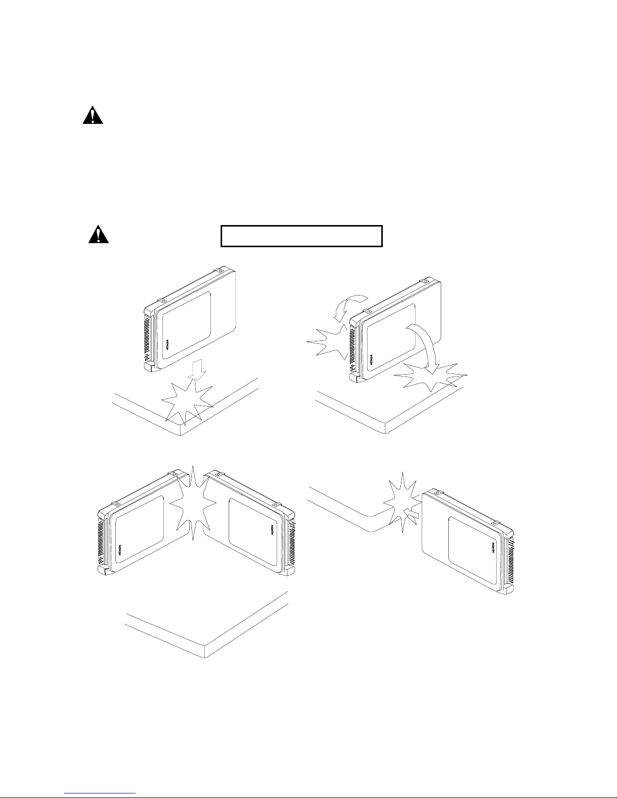
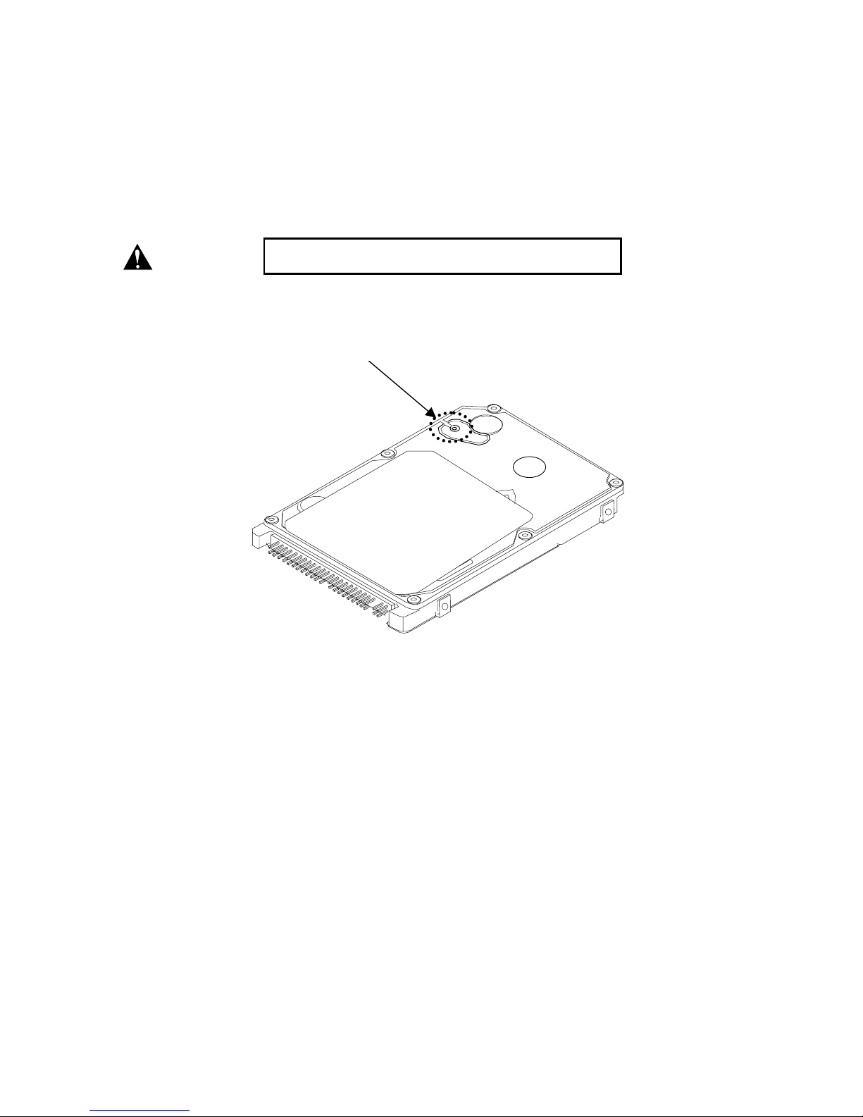
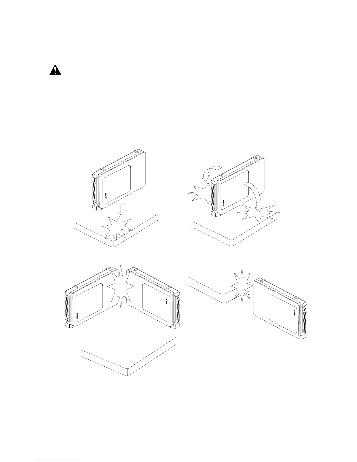
1.2 General Caution
Adhere to the following cautions.
(a) Warranty void if Metal Head Disk Assembly (HDA) is opened, or any HDA seal/label is broken.
(b) Hot swapping (Power on) damages the drive. The drive should be swapped during Power O ff only.
(C) Shock can result in permanent damage to the drive and/or loss of data.
Prevent shocks often incurred by dropping, knocking over, or hitting the drive.
(Dropping) (Knocking over)
(Hitting) (Hitting)
Figure 1-1
Caution
PREVENT SHO CK S
Caution
K6602637
Rev.3
02.27.01
- 11 -
(Continued)
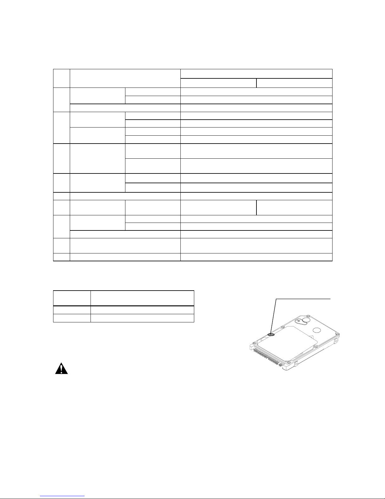
(d) Do not cover the breather hole. If the hole was covered w ith any material, it shall result in permanent
damage to the drive and/or loss of data. Label or seal shall be attached on the cover avoiding the
breather hole. Warranty void if the breather hole was covered.
Caution
Do not cover the breather hole
Breather hole
Figure 1-2 Breather hole location
K6602637
Rev.3
02.27.01
- 12 -
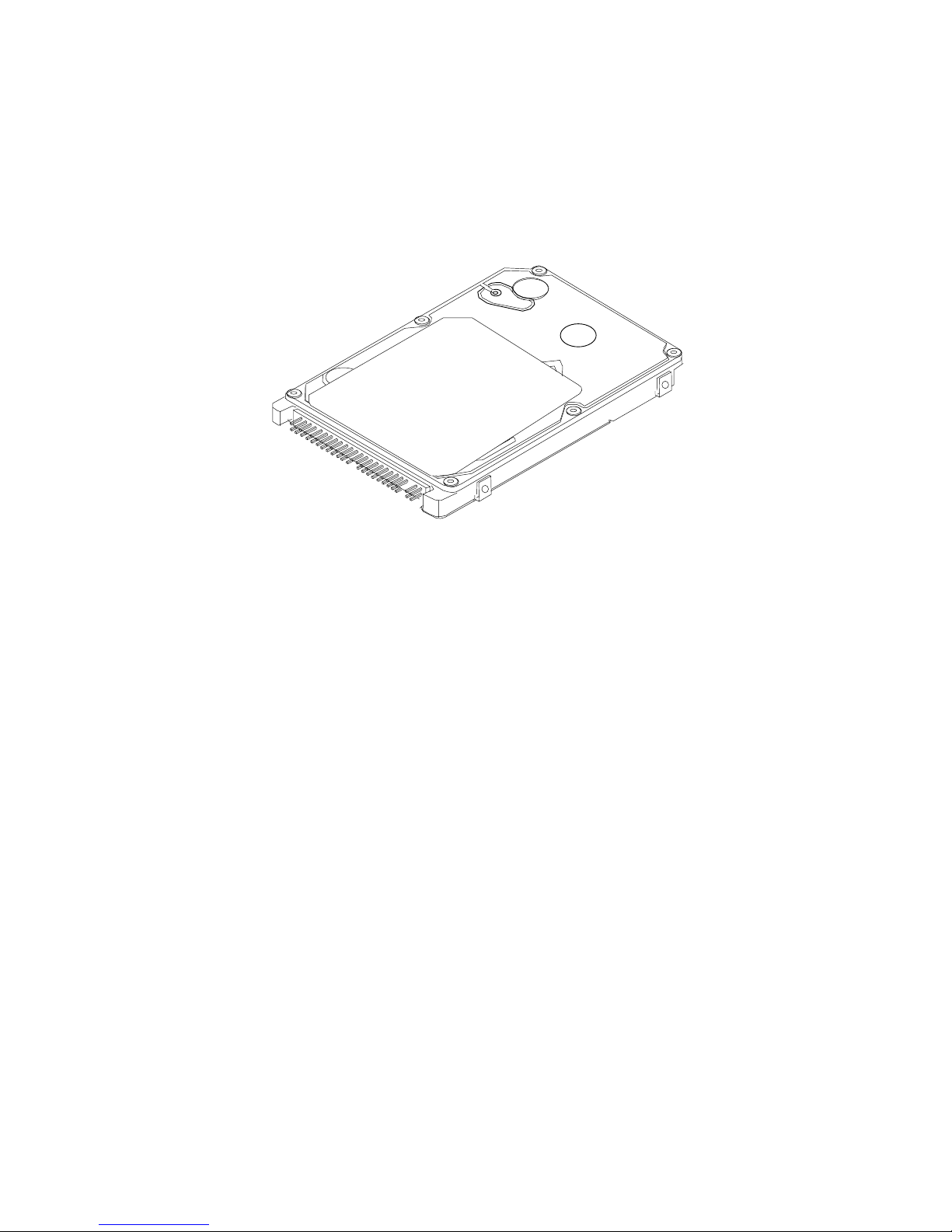
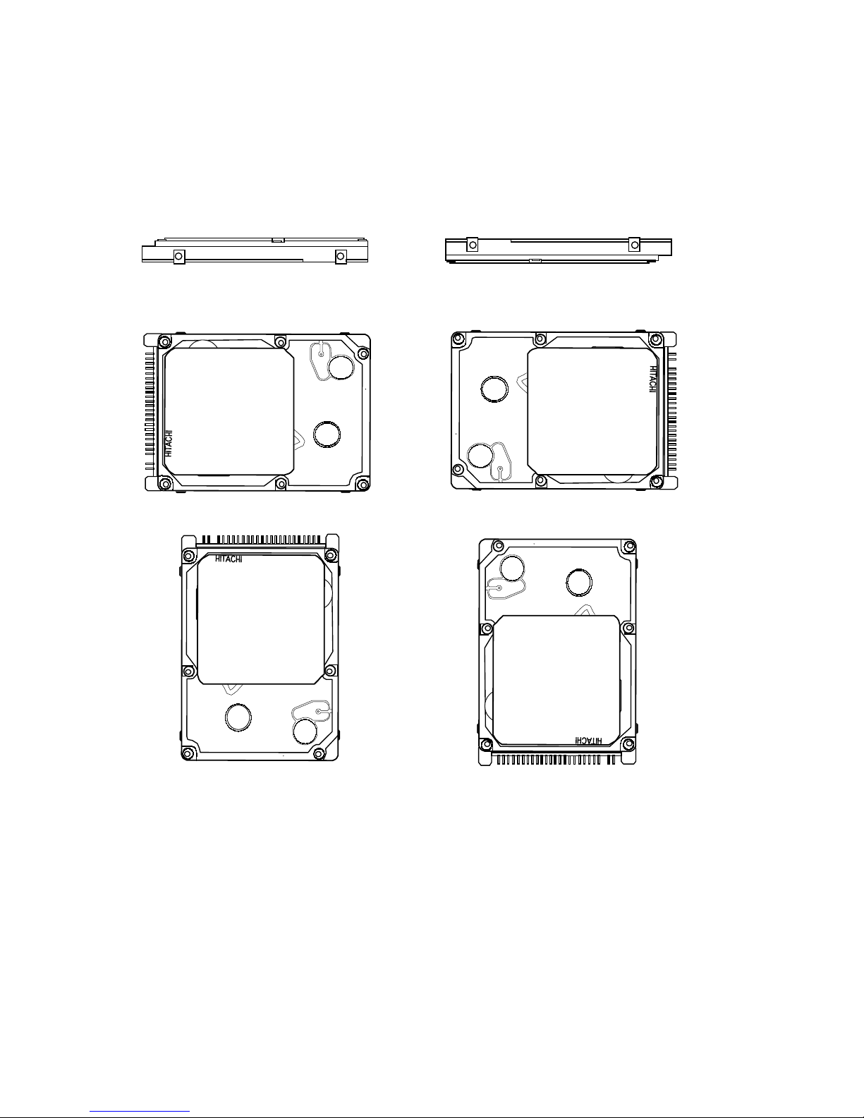
2.0 Components
DK23CA-30F/30/15/75 Disk Drive
Figure 2-1 Overview of DK23CA-30F/30/15/75 (9.5mm height)
Note: 1) Prepare connection cables referring to Sec. 6.2.
2) Mounting holes are compatible with DK237A-XX, DK238A-XX, DK239A-XX, DK23AA-XX
DK23BA-xx and DK23BA - XXE.
K6602637
Rev.3
02.27.01
- 13 -
3.0 Specification Summary
3.1 Principal Specifications
Table 3.1 Principal Specifications
Specifications
No. Item
DK23CA-30F/30 DK23CA-15 DK23CA-75
Units
1 Capacity per drive (Formatted
)
30,005 15,103 7,501 MB
Capacity per sector 512 Bytes
Disks 2 1 1
Heads 4 2 1
Cylinders 28,134
2 Seek time Average 12
*1
ms
(
Nominal Maximum 24
*1
ms
value
)
Minimum 3 ms
3Average latenc
y
7.1 ms
Disk rotational speed 4,200 RPM
4 Recording densit
y
Max. 530 kBPI
Track densit
y
46.8 kTPI
Recording method ME2PRML, ID-Less format
5 Interface ATA-5(IDE
)
Data transfer rate (Disk-Buffer
)
16.3 – 30.2 MB/sec
Data transfer rate (Host-Buffer
)
Max. 16.6 MB/sec
(
PIO mode 4/ Multiword DMA mode 2
)
Max. 100 (Ultra DMA mode 5
)
MB/sec
Buffer size 2048 512 512 kB
6 Power on - Ready
*2
5 (Typical)
*3
sec
Sleep/Standby - Ready
*2
3 (Typical)
*3
sec
7
Dimensions(W×H×D) 70W×9.5H×100D
mm
Weight (Approximate value
)
95 91 91
g
rams
8 DC Power Requirements
*4
(Typical)
+
5v ± 5% Ripple noise 100mvp-p or less
- Start up *5 0.90 A(4.5W)
- Idle *6 0.13 A(0.65W)
- Low Power Active *7 0.33 A(1.65W)
-Seek *8 0.45 A(2.25W)
- Read/Write *9 0.40/0.40 A(2.0/2.0W)
- Standby 0.050 A(0.25W)
- Sleep 0.020 A(0.1W)

K6602637
Rev.3
02.27.01
- 14 -
*1
:Average time of seek is calculated under the following condition. (Read/Write ratio: Read only)
Average of 10,000 random seeks, Voltage 5.0V, Temperature 25°C.
Maximum time of seek is calculated under the following condition.
Average of 1,000 full stroke seeks, Voltage 5.0V, Temperature 25°C.
This maximum time is not included the seek time by seek retry.
*2
: Periodically, during start up, the drive may perform a spin up retr y operation. When this operation occurs,
the start up sound will change slightly and the ready timing will also be altered from typical time.
*3
: Power on to Ready time could take up to 20 seconds in case of spin up retries under certain
conditions of the voltage specifications(Table 3.1) and environmental specifications(Table 3.2).
*4 :
For DC power input, the average current is measured at the connector of the PCBA of this drive and in
the nominal condition in which the power voltage and the temperature are 5.0V and 25°C, respectively.
Burst free (common mode). The average current may have some tolerance after power-on. The current
measurement is recommended at 5 minutes later after power-on.
Voltage rise time 5 - 100 ms at power on is required for power supply. The power
supply voltage must not be under below GND lev el ( 0 V) at power off.
This product is required over current protection for possible combustion due to
circuit or component failure. Secondary over current protection shall be prepared
by the system. The requirement of the current limitation is max. 10 A for the
protection.
*5
: For more information, refer to Section 6.1.
*6
: This value is at Low Power Idle mode. The heads are unloaded.
*7
: Power mode automatically enters to Low Power Active mode after Read/ Write operation. Head position
is kept on the same track before this power transition.
*8
: Measured during random seek , and the seek interval is 1.5 revolution times (i.e. the average latency
and one revolution).
*9
: Measured while reading or writing 16 sectors of data located on the same track.
Caution
Caution
K6602637
Rev.3
02.27.01
- 15 -
3.2 Environmental Specifications and Reliability
Table 3.2 Environmental Specification and Reliability
No. Item Specification
DK23CA-30F DK23CA-30/15/75
1
Ambient
*1
Operational
5 to 55°C
temperature Non-operational
-40 to 70°C
*2
Temperature gradient
Max. 20°C /hour
2 Relative humidity Operational 5 to 90 %
Non-operational 5 to 95 %
Maximum wet Operat ional
29°C (without condensation)
bulb Non-operational
40°C (without condensation)
*3
3 Vibration Operational 1.0mm p-p or less (5 - 22Hz)
9.8 m/s2 (1.0G) or less m/s2 (22 – 500Hz)
Non-operational 5mm p-p or less (5 – 22Hz)
49m/s2(5G) or less (22 – 500Hz)
4
Shock
*6
Operational
1,764m/s2(180G) or less (2 ms, half sine wave)
Non-operational
7,840m/s2(800G) or less (2 ms, half sine wave)
5 Atmospheric condition Without corrosive vapors or salt
6 Acoustic-noise
*4
Idle Typical 2.5 Bels Typical 2.8 Bels
7 Height Operational 3,000m or less
(Altitude) Non-operational 12,000m or less
Height gradient Max. 300m/min.(3.1kpa/min.)
8
(*5)
Data reliability
(with retries and ECC)
Less than 1 non-recoverable error in
10 E 13 bits read
9 External magnetic field 1,500 micro Tesla (DC) or less
*1
: Ambient temperature should be measured at point 10 mm away from the nameplate of the drive. If the
maximum operational ambient temperature cannot be measured at a point 10 mm away from the
nameplate, a substitution method is stipulated in the table below.
Ambient
temperature
Temperature at cover
(Point A)
55°C62
°
C
5°C5
°
C
*2
: In case the ambient temperature is -40 to 0°C, the drive should be
packed in HDD package box. Please see specification 5.1 Packing
for reference.
Maximum power-off interval is 12 months.
*3
: In case of the maximum wet bulb 40°C , the drive should be packed in HDD package box with ESD bag
and desiccant. Please see specification 5.1 Packing for reference. If the drive is not packed in the HDD
package box with ESD bag and desiccant, maximum wet bulb 29°C is applied.
Caution
Measurement point
(Point A
)

K6602637
Rev.3
02.27.01
- 16 -
*4
: 3.9 Bels are the maximum sound power levels with A-weighted . This value is specified at product
shipment, except during startup, seek, load, unload or st op. Clicking noise of releasing magnet latch will
occur at power-on and loading operation. Also, the licking noise of locking magnet latch will occur at
normal and emergency unloading operations.
*5
:
Data reliability is not to be used to compromise t he host system data backup.
For the HDD evaluation, long term operation is not r ecommended. In case of
evaluation, once or more unload operation by Power off , Standby or Sleep is
recommended within twelve hours’ power on time.
*6
: These shock specifications are defined for each axis. For non-operating rotational shock, the
specification is 15K radian/sec
2
or less (2 ms, half sine wave).
3.3 Drive Usage Condition Specifi cat i ons
The drive is designed for usage under the following conditions. Since reliability and product life depends on
usage conditions, please consult our sales representatives or application engineers if the drive may be
operated outside these conditions.
-Power on hours (POH) : Less than 160 hours/month
POH includes Sleep and Standby modes.
The heads are unloaded during Power off, Standby, Sleep or Low Power Idle
modes. The spindle motor is stopped during Standby and Sleep modes.
-Operating (Seek/Write : Less than 20% of POH
Read operations)
-Motor Start/Stop Count : Max. 100,000 times. This number includes Standby, Sleep and pow er-on/off
count.
-Environment : Within environmental specifications given in Table 3.2
-Power Requirement : Within DC power requirement specifications given in Table 3.1 “Principal
Specifications”
-Drive Grounding : Drive frame should be grounded to system ground with four screws electrically.
Grounding noise should be less than 500mVp-p. The grounding noise
should be measured between electrical ground and system frame ground
without the drive. Grounding AC current (measuring between two of side
mounting holes) should be less than 50 mAp-p (Frequency Range: less than
20MHz). The grounding current should be measured through 50 ohm resistor.
-External Magnetic Field : Within specifications given in Table 3.2
-Mounting : Mount with recommended screws and regular torque.
-Physical/Electrical Interface: ATA-5
-Handling : Do not add Electrical Static Discharge, and Vibration and Shock to the drive.
Do not press top cover and bottom PCBA surface of the drive.
Caution

K6602637
Rev.3
02.27.01
- 17 -
3.4 Load/Unload Specifications
Load /Unload is a mechanism to load/unload the heads on the disk surfaces.
3.4.1 Normal Load/Unload
Normal load/unload operations are limited to maximum 300,000 times during HDD life. The normal unload
operation is performed by the following commands.
-
Standby
-
Standby Immediate
-
Sleep
Also, the normal unload is automatically performed by control software, during Idle mode. The abov e normal
unload time does not include an emergency unload as explained in Sec. 3.4.2.
3.4.2 Emergency Unload
The emergency unload is occurred by unexpected power down, and is limited to maximum 20,000 times
during HDD life. Since normal unload can not be performed by the softwar e cont r o l aft er power off, the
heads are unloaded by a hardware control. The maximum number of emergency unload is defined
separately.
3.4.3 Required Power Off Sequence
To operate the load/unload normally, the following BIOS sequence is required by Host system before power
off.
[Sequence #1]: Execute one of following commands.
-
Standby
-
Standby Immediate
-
Sleep
Note:
Such as Soft Reset, Flush Cache command or Check Power Mode command does
not unload the heads. Soft Reset does not unload the heads from DK23CA-xx.
[Sequence #2]: Check the Status Register, and wait the command complete.
Note:
The head is unload by the sequence #1 command, and the command completion
normally takes about 400 ms. Considering the error retries, BIOS timer should be set
to over 30 sec by the Host side.
[Sequence #3]: Power off the drive
Above sequence is required for the Host system at Power off, Suspend and Hibernation operations.
K6602637
Rev.3
02.27.01
- 18 -
4.0 Installation
4.1 Installation Direction
The DK23CA-30F/30/15/75 can be installed in the 6 directions as shown below.
Figure 4-1 Installation
K6602637
Rev.3
02.27.01
- 19 -
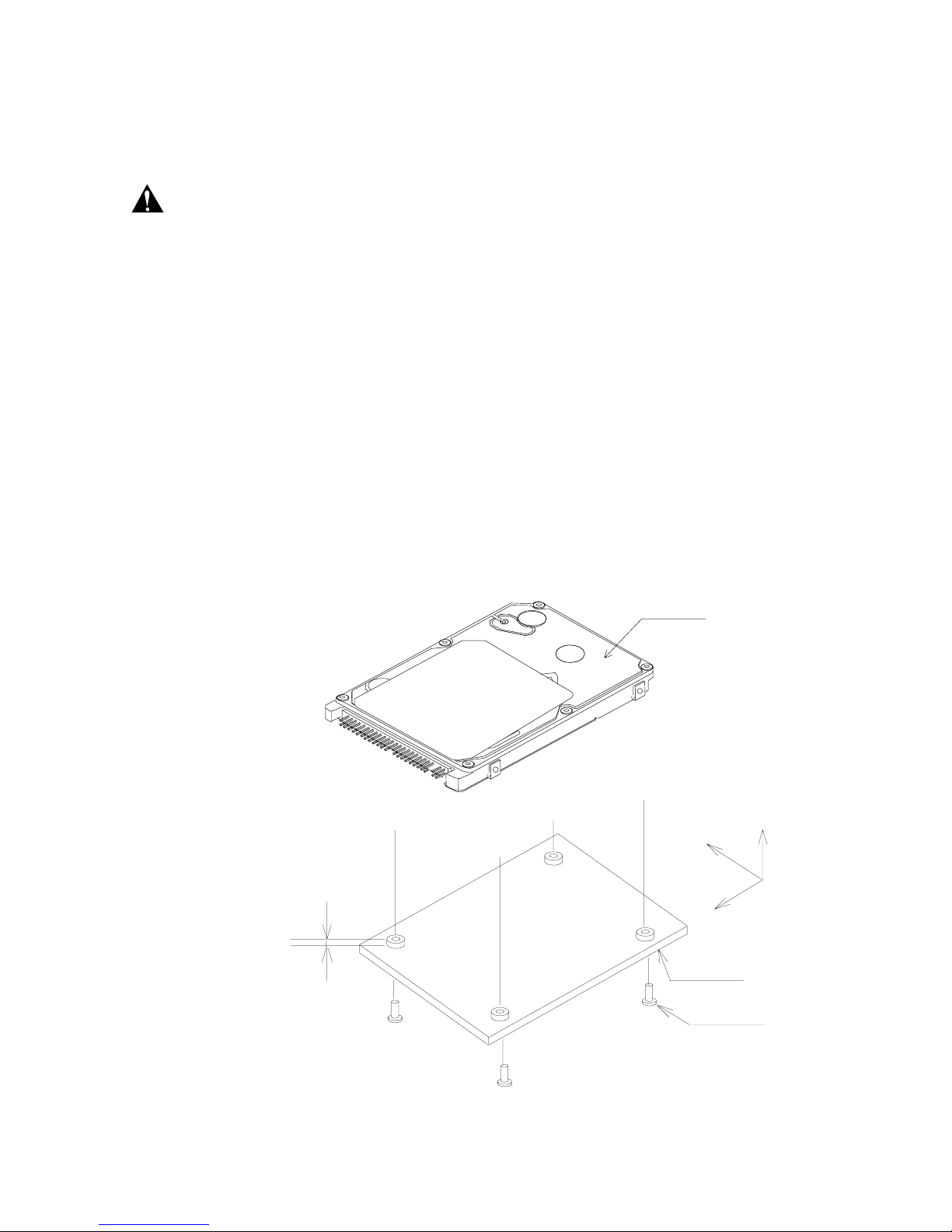
4.2 Mounting HDD
4.2.1 Mounting HDD with screws
Mount the HDD with the screws according to the following instruction to optimize the
performance.
(a) Mount the HDD with M3 screws. Take care not t o add any distorting force to the HDD when mounting.
Using 4 screws holes, secure the HDD.
(b) Use screws with the following specifications when t he HDD is mounted.
i) M3 (screw engagement of 2.5mm max)
ii) The torque for fixing the screws is 3±0.5kgcm(2.6±0.4 lb. inch)
(c) Any distortion of HDD over 0.020mm should be avoided. Take care that the system chassis are
flat enough.
(d) Consider an appropriate cooling to keep the temperature of cent er of HDD top cover less than 62°C.
(e) The inertia of the chassis around the Z-axis of the gravity center of the device must be more than
7 X 10
-4
kg m2.
Note) In case of general Sub-Notebook PC(Weight: 1.7kg), the inertia of the chassis around the Z-axis of
the gravity center of the device is greater t han 100 X 10
-4
kg
m2. Therefore, the required inertia level
has no problem with the general electronic equipment.
Caution
(0.2)
4-M3x0.5
Chassis
X
Z
Y
(
Unit: mm
)
HDD
Figure 4-2 Mounting the HDD
K6602637
Rev.3
02.27.01
- 20 -
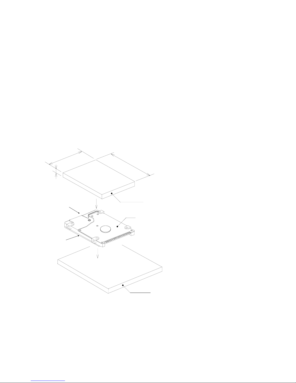
4.2.2 Single HDD Test Condition
To optimize the performance, keep the following instructions.
1) For the Single HDD test, HDD should be placed on an ABS-sheet. HDD should be place wit h
no movement by external force min. 0.39N for X axis and Y-axis directions.
2) Don’t place HDD on a soft sponge sheet or hard surface at HDD test. I f the HDD is placed on
the soft sponge sheet or slippery hard desk surface, the HDD has unstable condit ions such as HDD
self-vibration at seek operations or spindle motor rotation. It may cause performance reduction or
some errors. Also, HDD floating by t ension of I /F cabling may cause the similar symptom. The HDD
should be placed without any floating. Don’t test the HDD under these unstable conditions.
3) If the HDD cannot be fixed by the required holding torque above item 1), put a body weight on the
HDD as shown in Figure 4-3. The body weight is prov ided for pr eventing the HDD movement or HDD
floating by tension of I/F cabling.
Use the body weight as specified below.
Material : SS41 with ELP-coat
Weight : M=0.66kg
Inertia : I=7.3X10 kg m
Figure 4-3 Single HDD Test Condition
Y Axis Direction
X Axis Direction
(70)
(13)
(92)
Weight
SS41 with Insulation sheet
(m=0.66kg, I=7.3X10 kg m )
-4
2
HDD
ABS-sheet
(t = 5mm)
K6602637
Rev.3
02.27.01
- 21 -
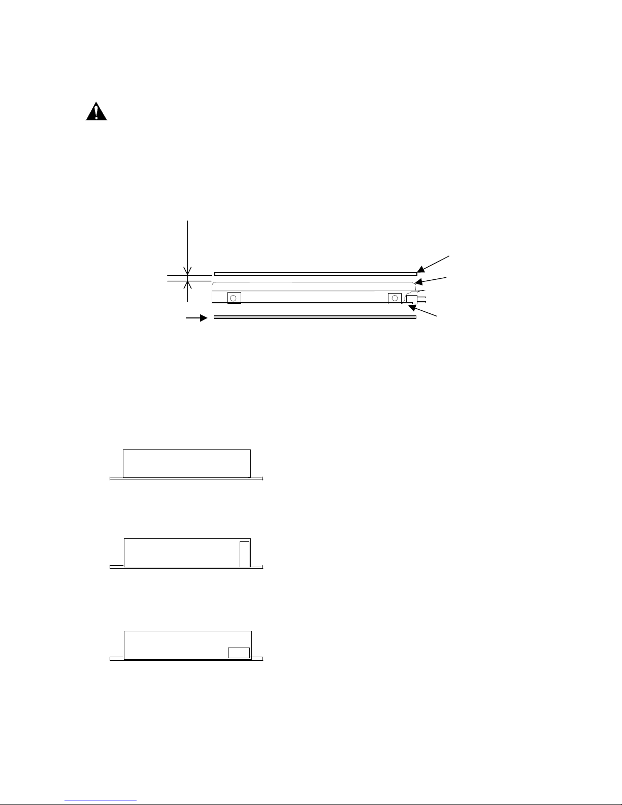
4.2.3 Attent i on f or HDD Installation
(1) In case of steel plate installation on HDD cover side, the spacing between
HDD cover and steel plate should be kept more than 2 mm. If this spacing is not
kept for the steel plate, it may affect Load/Unload mechanism.
(2) The PCBA side of the drive should be covered with insulation sheet if the active
metal of host system may contact to the PCBA of t he drive. If the insulation sheet
is not provided for the possible contact of the live metal, failures may occur.
(3) Do not push the bottom PCBA. It may cause catastrophic failures.
4.3 Device Address Setting (DRI VE 0/DRIVE 1)
When the device is connected to the host bus, Device address setting is necessary to configure
a device as DRIVE 0 or DRIVE 1. The device address setting is established bet ween drives on
the interface connector by using jumper 0-2 (pin # A, B, D)
The DRIVE 0 is assigned to device address 0, and the DRIVE 1 is assigned to device address 1.
O - - - - - - - - O O O O O
O - - - - - - - - O O O O O
43 5 3 1
CA
44
642 DB
O - - - - - - - - O O O O O
O - - - - - - - - O O O O O
43 5 3
1
CA
44 642 DB
O - - - - - - - - O O O O O
O - - - - - - - - O O O O O
43 5 3 1
CA
44 642 DB
1) DRIVE 0 (or single)
2) DRIVE 1
3) CSEL Selection
If all of pins A,B, D are open, the drive is
DRIVE 0(or single).
If jumper Position A-B is used, the driv e is
DRIVE 1.
If jumper Position B-D is used, DRIVE 0 or
DRIVE 1 settin g is deter mined b y the con dition of
CSEL signal (pin# 28).
Caution
Steel Plate
HDD Cover
2 mm
PCBA
More than
Insulation sheet
(Recommended type of jumper socket)
Vender: IRISO ELECTRONICS CO., LTD.
Vender Part Number: 9721HJ-GF
K6602637
Rev.3
02.27.01
- 22 -
±
0.25
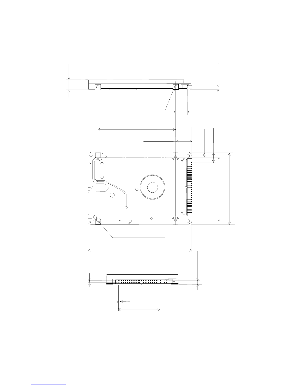
4.4 Dimensions
Figure 4-4 Dimensions (DK23CA-30F/30/15/75)
9.5
±
0.2
14.0 ± 0.25
4-M3
3.0mm min. full thread
10.14
±
0.375
100±0.45
61.72
±
0.25
(70.1
Maximum drive width
)
69.85
4.07
±
0.25
10.24 ± 0.25
3
±
0.25
4-M3
3.5mm min.
full thread
76.6 ± 0.25
2
3.99
±
0.25
2
42
(Unit : mm)
Drive width at mountin
g

K6602637
Rev.3
02.27.01
- 23 -
5.0 Packing and Handling
5.1 Packing
When you package the device, clean it and execute the following procedures
to prevent humidity and handling damage.
(1) Pack the device in an ESD protective bag with desiccant.
(2) Use the original Hitachi cardboard box and the cushioning materials or equivalent cushioning
structures to surround the above bag.
(3) Never stack or package drives next to each other with at the proper cushion material separating
them.
(4) Indicate which side is upside or downside on the exterior of the package box and attach notices
requesting careful treatment and preventing the box from being turned upside down.
(5) Prevent excessive pressure from being applied on the top and bottom of the drive(top cover and
PCBA side) when packing, unpacking, and transporting.
(6) Remember, mishandling of a drive can void the drive’s warranty.
Prevent humidity when the drive is packed in a box.
Caution
Caution
K6602637
Rev.3
02.27.01
- 24 -
5.2 Handling
Mount the HDD with the screws according to the following instructions to optimize the
performance.
It is necessary to prevent vibration, shock, and static electricity to the dr ive because it will damage the
precision parts. In particular, prevent vibration or shock generated by dropping, knocking over, or hitting the
drive. Also, avoid touching the electrical components directly, which can discharge electrostatic energy and
damage the drive.
(Dropping) (Knocking over)
(Hitting) (Hitting)
Figure 5-1
Caution
K6602637
Rev.3
02.27.01
- 25 -
6.0 Interface
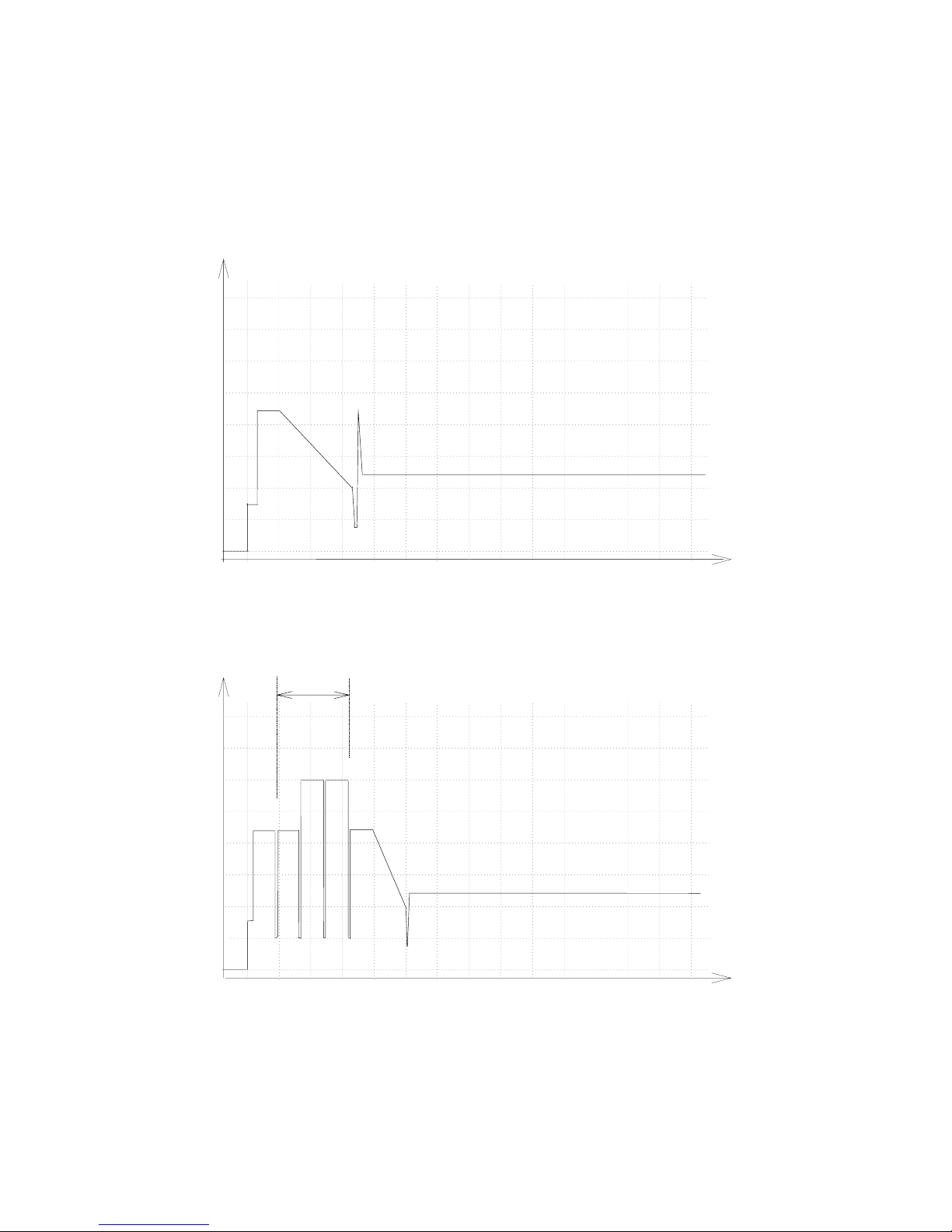
6.1 Power Interface
Only +5VDC power is applied to this Device. Figures 6-1 and 6-2 show power current transitions
after turning on the power.
Typical Spin-up Current Transition
1.6
1.4
1.2
1.0
0.8
0.6
0.4
0.2
0.0
0123456
7
Time (sec)
Current of
+5V power
(A)
Figure 6-1 Power Current Transition
Typical Spin-up Current Transition with Retry
1.6
1.4
1.2
1.0
0.8
0.6
0.4
0.2
0.0
0
123456
7
Time (sec)
Current of
+5V power
(A)
8
9
10 11
121413
Retry
Figure 6-2 Power Current Transition with retries
K6602637
Rev.3
02.27.01
- 26 -
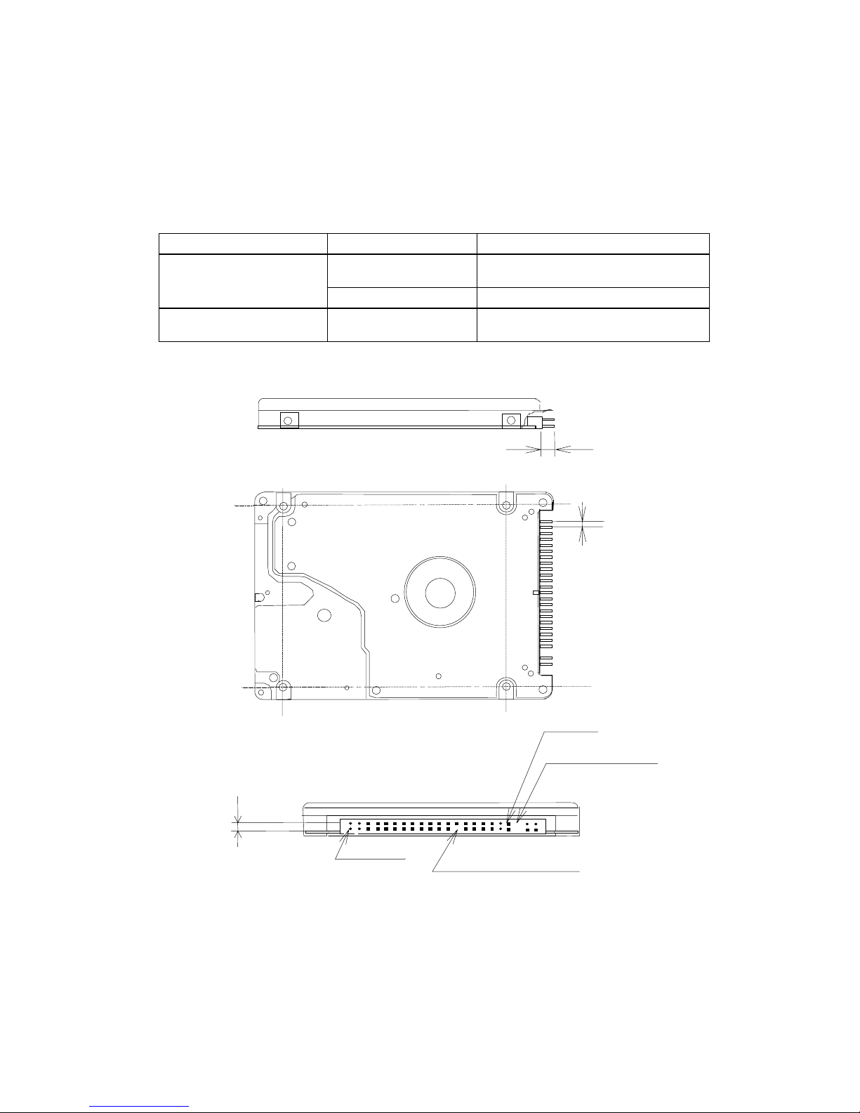
6.2 Physical Interface
6.2.1 Connector
This device has a 2mm pitch interface connector which contains a power line. The connector
location is shown in Figure 6-3.
Table 6.1 Connector Parts List
Name Parts number of recommended type
Interface cable side
Signal Connector
Receptacle
Molex 87259-4413 or equivalent
Cable AWG#28 or equivalent
Drive side
Signal Connector
Plug
Molex 87400-5005 or equivalent
Figure 6-3 Connector Location
2 mm
PIN44
PIN20 REMOVED(KEY)
PINS REMOVED(KEY)
PIN1
3.86 mm
2 mm

K6602637
Rev.3
02.27.01
- 27 -
6.2.2 Connector Pin Assignment
Figure 6-4 Pin Assignments
JUMPER0
JUMPER2
KEY(Removed)
DD7
RESET-
DD6
DD5
DD4
DD3
DD2
DD1
DD0
GND
DMARQ
DIOW-
DIOR-
IORDY
DMACK-
DA1
DA0
CS0-
DASP-
5VDC(Logic)
GND(Logic)
A
C
E
1
3
5
7
9
11
13
15
17
19
21
23
25
27
29
31
33
35
37
39
41
43
B
D
F
2
4
6
8
10
12
14
18
16
20
22
24
28
32
26
30
34
36
38
40
42
44
JUMPER1
JUMPER3
KEY(Removed)
GND
DD8
DD9
DD10
DD11
DD12
DD13
DD14
DD15
KEY(Removed)
GND
GND
GND
CSEL
GND
IOCS16PDIAGDA2
CS1GND(Motor)
5VDC(Motor)
Reserved
INTRQ
PCB
K6602637
Rev.3
02.27.01
- 28 -
6.2.3 Description of the Interface Signals
The interface is an ATA(IDE) interface. Reserved pins should be left unconnected. The signal names
and the pin numbers are shown in Figure 6-4 and Table 6.2. Table 6.2 shows signal definitions.
"I" of I/O type represents an input signal from the device and "O" represents an output signal from the
device.
Table 6.2 Signal List(1/3)
Signal name Pin I/O type Description
RESET- 1 I This is a reset signal output from the host system and to be
used for interface logic circuit.
DD0-DD15 3-18 I/O This is a 16-bit bi-directional data bus. The lower 8 bits are
used for register access other than data register.
DIOW- 23 I The rising edge of this Write Strobe signal clocks data from
the host data bus into a register on the device.
STOP
*1
Assertion of this signal by the host during an Ultra DMA burst
signals the termination of the Ultra DMA burst.
DIOR- 25 I Activating this Read Strobe signal enables data from a register
on the device to be clocked onto the host data bus. The rising
edge of this signal latches data at the host.
HDMARDY-
*1
This signal is a flow control signal for Ultra DMA Read.
Host asserts this signal, and indicates that the host is ready t o
receive Ultra DMA Read data .
HSTROBE
*1
This signal is Write data strobe signal from the host for an
Ultra DMA Write. Both the rising and falling edge latch
the data from DD(15:0) into the device.
IORDY 27 O This signal is used to temporarily stop the host register access
(read or write) when the device is not ready to respond t o a
data transfer request.
DDMARDY-
*1
This signal is a flow control signal for Ultra DMA Write. Device
asserts this signal, and indicates that the device is ready t o
receive Ultra DMA Write data .
DSTROBE
*1
This signal is the data in strobe signal from the device for an
Ultra DMA Read. Both the rising and falling edge latch
the data from DD(15:0) into the host.
CSEL 28 I This signal is used to configure a device as either DRIVE 0 or
DRIVE1 when CSEL mode is selected.
This signal is pulled up inside the drive.
CSEL
GND
OPEN
0
1
Drive address
*1
: Signal name in Ultra DMA mode

K6602637
Rev.3
02.27.01
- 29 -
Table 6.2 Signal List(2/3)
Signal name Pin I/O type Description
INTRQ 31 O This is an interrupt signal for the host system. This signal is
asserted by a selected device when the nIEN bit in the Device
Control Register is "0". In other cases, this signal should be a high
impedance state.
IOCS16- 32 O This signal indicates to the host that the 16-bit data port has been
addressed and a 16-bit word can be read or written to the device.
DA0-2 33,35,36 I This is a register address signal from the host system.
PDIAG-:CBLID-
(*1)
34 I/O The PDIAG- signal is asserted by Device 1 to indicate to Device 0
that it has completed diagnostics. This signal is pulled up inside the
device.
The host may sample CBLID- after a power-on or hardware reset in
order to detect the presence or absence of an 80-conductor cable
assembly by performing the following steps:
a) The host shall wait until the power on or hardware reset
sequence is complete for all devices on the cable;
b) If Device 1 is present, the host should issue IDENTIFY DEVI CE
or IDENTIFY PACKET DEVICE and use the returned data to
determine that Device 1 is compliant with ATA-3 or subsequent
standards. Any device compliant with ATA-3 or subsequent
standards releases PDIAG- no later than after the first
command following a power on or hardware reset sequence.
If the host detects that CBLID- is connected to ground, an 80conductor cable assembly is installed in the system. If the host
detects that this signal is not connected to ground, an 80-conductor
cable assembly is not installed in the system.
CS0- 37 I This device chip selection signal is used to select the Command
Block Registers from the host system.
CS1- 38 I This device chip selection signal is used to select the Control Block
Registers from the host system.
*1
: PDIAG-:CBLID- (Passed diagnostics: Cable assembly ty pe identifier

K6602637
Rev.3
02.27.01
- 30 -
Table 6.2 Signal List(3/3)
Signal name Pin I/O type Description
DASP- 39 I/O This signal indicates that a device is active or that Drive 1 is present
when the power is turned on.
Upon receipt of a command from the host, the device asserts this
signal. At command completion, the device de-asserts this signal.
However, When a sequential read command is received from the
host, the device does not assert this signal.
DMARQ 21 O The device shall assert this signal, used for DMA data transfers
between host and device, when it is ready t o t r ansfer dat a.
DMACK- 29 I The host in response to DMARQ to either acknowledge that data
has been accepted, or that data is available shall use this signal.
JUMPER0,1,2 PIN-A,B,D - See Sec. 4.3 “ Drive Address Setting (Drive 0/Drive 1)” for the detail.
The I/O signal levels are as follows.
(1) Input signal High level +2.0V to Vcc+0.5V
Low level -0.5V to +0.8V
(2) Output signal High level +2.4V to +5.25V or an open circuit
Low level +0.4V or less (IOL=2mA), +0.5V or less (IOL=12mA)
Note) The I/F cable should be no longer than 50cm(20 inches) including the circuit pattern length in the host
system. If the cable length is not within this specification, it may cause fact ional degradat ions or some
errors.

K6602637
Rev.3
02.27.01
- 31 -
6.3 Logical Interface
6.3.1 I/O Registers
Communication between the host system and the device is done through I/O registers. The Command
Block Registers are used for sending commands to the device or posting device status. The Control
Block Registers are used for controlling the device or posting device status. The registers are listed in
Table 6.3.
Table 6.3 Register List
Addresses Functions
CS0- CS1- DA2 DA1 DA0 READ(DIOR-) WRITE(DIOW-)
Command Block Registers
01000Data Data
0 1 0 0 1 Error Features
0 1 0 1 0 Sector Count Sector Count
0 1 0 1 1 Sector Number Sector Number
0 1 1 0 0 Cyl Low Cyl Low
0 1 1 0 1 Cyl High Cyl High
0 1 1 1 0 Device/Head Dev ice/ Head
01111Status Command
Control Block Registers
1 0 1 1 0 Alt. Status Device Control
Invalid or Not Used
00
´´´
Invalid address
01
´´´
Data bus high impedance (not used)
100
´´
Data bus high impedance (not used)
1010
´
Data bus high impedance (not used)
'0' is low signal level. '1' is high signal level.
6.3.1.1 Data register
A 16-bit register to be used for transferring dat a blocks betw een the HDD's data buffer and the host.
6.3.1.2 Error register
This register stores device status when the last command has been completed or diagnostic codes
when a self-diagnostic process has been completed. The contents of this register are valid when the
error bit (ERR) is set in the Status Register. The contents of this register are diagnostic codes when
the device has just completed a self-diagnostic process requested when turning on the power or
resetting.

K6602637
Rev.3
02.27.01
- 32 -
Bit76543210
Name ICRC UNC - IDNF - ABRT TK0NF AMNF
a) AMNF(Address Mark Not Found): This bit indicates that a data address mark is not found after the
correct ID field is detected.
b) TK0NF(Track 0 Not Found): This bit indicates that Track 0 is not found during the execution of the
Recalibrate command.
c) ABRT(Aborted Command): This bit indicates that execution of a command is interrupted due to
a device error(e.g. Not Ready and Write fault) or an invalid command code.
d) IDNF (ID Not Found): This bit indicates that an ID field of the requested sect or is not found.
e) UNC(Uncorrectable Data Error): This bit indicates that an uncorrectable error has occurred.
f) ICRC(Interface CRC Error): This bit indicat es that an interface CRC error was occurred. This bit is not
applied for Multiword DMA transfers.
6.3.1.3 Features Register
By combining with the Set Features command, this register is used for enabling or disabling each
feature.
6.3.1.4 Sector Count Register
This register contains the number of sectors of data requested to be transferred on a read or write
operation. When a command has been completed and the value of this register is "0", it represents that
the command has been executed successfully. If the command has not been executed successfully,
this register indicates the number of the sectors yet to be processed. This definition cannot be applied
to all commands. For more information on commands, refer to the corresponding sections.
6.3.1.5 Sector Number Register
This register contains the starting sector number for any disk data access. This number may be from 1
to the maximum number of sectors per track. In LBA mode, this register contains Bits 7-0 of the LBA.
6.3.1.6 Cylinder Low Register
This register contains the lower 8 bits of the starting cylinder address for any disk access. When a
command has been executed; this register displays the currently specified cylinder number.
In LBA mode, this register contains Bits 15-8 of the LBA.
6.3.1.7 Cylinder High Register
This register contains the higher 8 bits of the starting cylinder address for any disk access. When a
command has been executed, this register displays the currently specified cylinder number.
In LBA mode, this register contains Bits 23-16 of the LBA.

K6602637
Rev.3
02.27.01
- 33 -
6.3.1.8 Device/Head Register
This register has the binary coded address of device and head selected. The head numbers begins
with "0".
Bit76543210
Name - L - DRV HS3 HS2 HS1 HS0
a) Bits HS3 to HS0 are head addresses to be selected. HS3 is the highest bit. The address of the
currently selected head is displayed in this register when a command is completed. In case of
LBA mode, these bits HS3 to HS0 are applied to LBA bits 27 to 24.
b) DRV is a device selection bit. 0=DRV0, 1=DRV1
c) L is the sector address mode select. 0=CHS mode, 1=LBA mode
6.3.1.9 Status Register
The current device status is reflected in this register. The contents are updat ed at the completion of each
command. If BSY=1, no other bits in this register are valid. When BSY is cleared, the other bits in this
register shall be valid within 400 ns. If the host reads this register when an int errupt is pending, it is
considered to be the interrupt acknowledge, and the pending interrupt is then cleared.
Bit76543210
Name BSY DRDY DWF DSC DRQ CORR IDX ERR
a) ERR (Error): This bit indicates that an error occurs during the execution of a command. For more
information, refer to the description of the Error register.
b) IDX(Index): This bit is set once per disk revolution.
c) CORR(Corrected Data): This bit indicates that a correctable error has occurred and data has been
corrected. The data transfer is not interrupted.
d) DRQ(Data Request): This bit indicates that the dev ice is ready to transfer data between the host and
the device.
e) DSC(Device Seek Complete): This bit indicates that the device head is located on the specified track.
If an error has occurred, the value of this bit is not changed until the host reads the Status register.
f) DFW(Device Write Fault): This bit indicates that an error has occurred during a Write operation. If an
error has occurred, the value of this bit is not changed until the host reads the St atus register.
g) DRDY(Device Ready): This bit indicat es that the device is ready to respond any command. If an error
has occurred, the value of this bit is not changed until the host reads the St atus register. This bit is
cleared when the power is turned on and then kept cleared until the device gets ready t o accept any
command.
h) BSY(Busy): This bit is specified when the device accesses t he Command Block Registers. When BSY
is 1,the host cannot access the Command Block Registers. If the Command Block Registers are read
when BSY is 1, all contents of the Status Register are returned.
6.3.1.10 Command Register
The command code is sent to this register. After it is written, execution begins.

K6602637
Rev.3
02.27.01
- 34 -
6.3.1.11 Alternate Status Register
The information in this register is a duplicate of that in the Status Register. Reading this register will not
clear the interrupt.
6.3.1.12 Device Control Register
This register includes the software reset bit and the interrupt enable bit.
Bit76543210
Name - - - - - SRST nIEN '0'
a) nIEN(Interrupt Enable): If the device is selected when nI EN is 0, t he I NTRQ signal is enabled. When
nIEN is 1 or when the device is not selected, the I NTRQ signal is in a high impedance stat e.
b) SRST (Software Reset): When this bit is set, the device is reset. When this bit is cleared, the device
exits from the reset state. When two devices are connected through one line in the daisy chain mode,
they are reset simultaneously.

K6602637
Rev.3
02.27.01
- 35 -
6666
.3.2 Commands
6.3.2.1 Command Summary
Commands are issued to the device first loading the Command Block Registers with any information
needed for the command. Then a command code is written to the Command Register, which starts
the execution of the command.
Table 6.4 Command Codes
Command Description Protocol Class Code Parameter Setup
FR SC SN CY DH
Read Commands
Read Buffer PI 1 E4h D
Read Sectors PI 1 20h, 21h V V V V
Read Long PI 1 22h, 23h V V V V
Read Multiple PI 1
C4h
VVVV
Read DMA DM 1 C8h, C9h V V V V
Read Verify ND 1 40h, 41h V V V V
Write Commands
Write Buffer PO 2 E8h D
Write Sectors PO 2 30h, 31h V V V V
Write Long PO 2 32h, 33h V V V V
Write Multiple PO 3 C5h V V V V
Write DMA DM 3 CAh,CBh V V V V
Format Track PO 2 50h V V V
Flush Cache ND 1 E7h D
Seek Commands
Recalibrate ND 1 1Xh D
Seek ND 1 7Xh V V V
Mode Set/Check, Diagnostic
Execute Device Diagnostic ND 1 90h D
Initialize Device Parameters ND 1 91h V V
Identify Device PI 1 ECh D
Set Features ND 1 EFh V D
Set Multiple Mode ND 1 C6h V D
Power Control
Check Power Mode ND 1 98h, E5h V D
Idle ND 1 97h, E3h V D
Idle Immediate ND 1 95h, E1h D
Sleep ND 1 99h, E6h D
Standby ND 1 96h, E2h V D
Standby Immediate ND 1 94h, E0h D

K6602637
Rev.3
02.27.01
- 36 -
Table 6.4 Command Codes (Continued)
Command Description Protocol Class Code Parameter Setup
FR SC SN CY DH
SMART Commands
SMART Enable/Disable Auto
Save
ND 1 B0h D2h V V D
SMART Save Attribute
Values
ND 1 B0h D3h V D
SMART Enable Operations ND 1 B0h D8h V D
SMART Disable Operations ND 1 B0h D9h V D
SMART Return Status ND 1 B0h DAh V D
SMART Enable/Disable
Automatic Off-line
ND 1 B0h DBh V V D
SMART Execute Off-line
Immediate
ND 1 B0h D4h V D
SMART Read Log Sector PI 1 B0h D5h V V V D
SMART Write Log Sector PO 3 B0h D6h V V V D
Security Commands
Security Disable Password PO 3 F6h D
Security Erase Prepare ND 1 F3h D
Security Erase Unit PO 3 F4h D
Security Freeze Lock ND 1 F5h D
Security Set Password PO 3 F1h D
Security Unlock PO 3 F2h D
Protected Area Commands
Read Max Address ND 1 F8h D
Set Max Address ND 1 F9h 00h V V V D
Set Max Set Password PO 3 F9h 01h D
Set Max Lock ND 1 F9h 02h D
Set Max Unlock PO 3 F9h 03h D
Set Max Freeze Lock ND 1 F9h 04h D
PI : PIO Data In PO : PIO Data Out
ND : Non-Data DM : DMA Data In/Out
CY : Cylinder Registers SC : Sector Count Register
DH : Device/Head Register SN : Sector Number Register
FR : Features Register
V : Valid parameter register for this command D : Only the Device parameter is valid.

K6602637
Rev.3
02.27.01
- 37 -
6.3.2.2 Command BSY Timing
The manner in which a command is accepted varies by the three classes of command acceptance all
predicated on the fact that to receive a command, BSY=0. The following describes by t he condit ions
under which busy is set after receipt of a command.
Class1 - The device sets busy within 400 ns.
Class2 - The device will set BSY within 400 ns, t hen set s up t he sector buffer for a write operation,
then sets DRQ, and clears BSY within 400 ns of setting DRQ .
Note
: DRQ may be set so quickly on classes 2 that the BSY transit ion is t oo short for BSY=1 to
be recognized.
6.3.2.3 PIO Data In Commands
Execution includes the transfer of one or more 512 byte sectors of data from the device to t he host .
1) The host writes any required parameters to the Features, Sector Count , Sect or Number, Cylinder
Low, Cylinder High, and Device/Head registers.
2) The host writes the command code to the Command Register.
3) The device sets BSY and prepares for data transfer.
4) When a sector(block) of data is available, the device sets DRQ and clears BSY prior to asserting
INTRQ.
5) After detecting INTRQ, the host reads the Status Register, t hen reads one sect or (block) of data via
the Data Register. In response to the Status Register being read, t he device negates INTRQ.
6) The device clears DRQ. If transfer of another sector (block) is required, the device also sets BSY
and the above sequence is repeated from 4).

K6602637
Rev.3
02.27.01
- 38 -
6.3.2.3.1 Identify Dev i ce [ECh]
The Identify Device command enables the host to receive parameter information from the device.
When the command is issued, the device sets BSY, stores the required parameter information in the
sector buffer, sets DRQ, and generates an interrupt. The host then reads the information from the
sector buffer through the Data Register. The parameter words are defined in Table 6.5 and 6.6.
All reserved bits or words shall be zero.
Table 6.5 Identify Device Information
Word Description Value
(HEX.)
0 General configuration 045Ah
1 Number of logical cylinders See table 6.6
2 Specific configuration C837h
3 Number of logical heads See table 6.6
4 Number of unformatted bytes per track
5 Number of unformatted bytes per sector
6 Number of logical sectors per logical track See table 6.6
7-9 Vendor specific
10-19 Serial number (20 ASCII characters)
20 Buffer type
0000h = Not specified 0001h = Single port single buffer
0002h = Dual port multi-sector buffer
0003h = Dual port multi-sector buffer with read caching capability
0003h
21 Buffer size in 512 byte increments (0000h=not specified) DK23CA-15/
75: 0400h
DK23CA-30F/
30: 1000h
22 Number of ECC bytes passed on READ/WRITE LONG commands 0004h
23-26 Firmware revision(8 ASCII Characters)
27-46 Model number(40 ASCII Characters)
47 Number of sectors on multiple commands
Bit 15 - 8 80h (fixed)
Bit 7 - 0 Number of sectors on multiple command
8010h
48 Double word I/O not supported
0000h = cannot perform double word I/O
0001h = can perform double word I/O
0000h
49 Capabilities
Bit 15 – 14 0 = Reserved
Bit 13 1 = Standby timer values as specified in ATA-2
specification supported
Bit 12 0 = Reserved
Bit 11 1 = IORDY supported
Bit 10 1 = IORDY can be disabled
Bit 9 1 = LBA supported
Bit 8 1 = DMA supported
Bit 7 – 0 Vendor Specific
0B00h

K6602637
Rev.3
02.27.01
- 39 -
Table 6.5 Identify Device Information (
Continued)
Word Description Value
(HEX.)
50 Capabilities
Bit 15 0 (fixed)
Bit 14 1 (fixed)
Bit 13 - 1 0 = Reserved
Bit 0 1 = Standby timer value is equal to or greater than
5 minutes. Reserved.
4000h
51 Bit 15 - 8 PIO data transfer cycle timing mode
Bit 7 - 0 Vendor Specific
0200h
52 Bit 15 – 8 DMA data transfer cycle timing mode
Bit 7 – 0 Vendor Specific
0200h
53 Field validity
Bit 15 - 3 0 = Reserved
Bit 2 1 = The field reported in word 88 is valid
Bit 1 1 = The fields reported words 64-70 are valid
Bit 0 1 = The fields reported words 54-58 are valid
0007h
54 Number of current cylinders
55 Number of current heads
56 Number of current sectors per track
57-58 Current capacity in sectors
59 Multiple sector setting
Bit 15-90 = Reserved
Bit 8 1 = Multiple sector setting is valid
Bit 7 - 0Current setting for number of sectors that can be
transferred per interrupt on R/W MULTIPLE command
60-61 Total addressable LBA See table 6.6
62 Single word DMA transfer
Bit 15 - 8 Single word DMA transfer mode active
Bit 7 - 0Single word DMA transfer mode supported
63 Multi-word DMA transfer
Bit 15 - 8 Multi-word DMA transfer mode active
Bit 7 - 0Multi-word DMA transfer mode supported
64 Flow control PIO transfer Modes supported
Bit 15 - 2 0 = Reserved
Bit 1 1 = PIO Mode 4 supported
Bit 0 1 = PIO Mode 3 supported
0003h
65 Minimum Multi-word DMA Transfer Cycle Time Per Word(ns) 0078h
66 Manufacturer's Recommended Multi-word DMA Cycle Time(ns) 0078h
67 Minimum PIO Transfer Cycle Time without Flow Control(ns) 0190h
68 Minimum PIO Transfer Cycle Time with IORDY(ns) 0078h
69-74 Reserved 0000h
75 Queue Depth
Bit 15 - 5 0 = Reserved
Bit 4 - 0 Maximum queue depth
0000h
76-79 Reserved 0000h

K6602637
Rev.3
02.27.01
- 40 -
Table 6.5 Identify Device Information (
Continued)
Word Description Value
(HEX.)
80 ATA Interface Major Version Number
Bit 15 - 6 Reserved for ATA-6 - 14
Bit 5 1 = Supports ATA-5
Bit 4 1 = Supports ATA-4
Bit 3 1 = Supports ATA-3
Bit 2 1 = Supports ATA-2
Bit 1 1 = Supports ATA-1
Bit 0 Reserved
003Eh
81 ATA Interface Minor Version Number 0013h
82 Command Set Supported
0000h or FFFFh = Command set notification not supported
Bit 15 0 = Reserved
Bit 14 1 = NOP command supported
Bit 13 1 = READ BUFFER command supported
Bit 12 1 = WRITE BUFFER command supported
Bit 11 0 = Reserved
Bit 10 1 = Host Protected Area feature set supported
Bit 9 1 = DEVICE RESET command supported
Bit 8 1 = SERVICE interrupt supported
Bit 7 1 = Release interrupt supported
Bit 6 1 = Look-ahead supported
Bit 5 1 = Write cache supported
Bit 4 1 = Supports PACKET command feature set
Bit 3 1 = Supports power management feature set
Bit 2 1 = Supports removable feature set
Bit 1 1 = Supports security feature set
Bit 0 1 = Supports SMART feature set
346Bh
83 Command set supported
0000h or FFFFh = Command set notification not supported
Bit 15 0 (fixed)
Bit 14 1 (fixed)
Bit 13 - 9 0 = Reserved
Bit 8 1 = SET MAX security extension supported
Bit 7 1 = Address offset mode feature supported
Bit 6 1 = SET FEATURES subcommand required to spin-up after
power-up
Bit 5 1 = Power-up in standby feature set supported
Bit 4 1 = Removable Media Status Notification feature set supported
Bit 3 1 = Advanced Power Management feature set supported
Bit 2 1 = CFA feature set supported
Bit 1 1 = READ/WRITE DMA QUEUED supported
Bit 0 1 = DOWNLOAD MICROCODE command supported
4188h
84 Command set/feature supported extension
0000h or FFFFh = Command set notification not supported
Bit 15 0 (fixed)
Bit 14 1 (fixed)
Bit 13 - 0 0 = Reserved
4000h

K6602637
Rev.3
02.27.01
- 41 -
Table 6.5 Identify Device Information (
Continued)
Word Description Value
(HEX.)
85 Command set/feature enabled
0000h or FFFFh = Command set notification not supported
Bit 15 0 = Reserved
Bit 14 1 = NOP command supported
Bit 13 1 = READ BUFFER command supported
Bit 12 1 = WRITE BUFFER command supported
Bit 11 0 = Reserved
Bit 10 1 = Host Protected Area feature set supported
Bit 9 1 = DEVICE RESET command supported
Bit 8 1 = SERVICE interrupt enabled
Bit 7 1 = Release interrupt enabled
Bit 6 1 = Look-ahead enabled
If word 85 bit 6 is set to one, read look-ahead
has been enabled via SET FEATURE command.
Bit 5 1 = Write cache enabled
If word 85 bit 5 is set to one, write cache
has been enabled via SET FEATURE command.
Bit 4 1 = Supports PACKET command feature set
Bit 3 1 = Supports power management feature set
Bit 2 1 = Supports removable feature set
Bit 1 1 = Supports Security Mode feature enabled
If word 85 bit 1 is set to one, the Security Mode
feature has been enabled via SECURITY SET PASSWORD
command.
Bit 0 1 = Supports SMART feature enabled
If word 85 bit 0 is set to one, the SMART feature
set has been enabled via SMART ENABLE OPERATIONS
command.
3468h
(at shipment)
86 Command set/feature enabled
0000h or FFFFh = Command set notification not supported
Bit 15 –9 0 = Reserved
Bit 8 1 = SET MAX security extension enabled by SET MAX
PASSWORD
Bit 7 1 = Address offset mode feature enabled
Bit 6 1 = SET FEATURES subcommand required to spin-up after
power-up
Bit 5 1 = Power-up in standby feature set enabled
Bit 4 1 = Removable Media Status Notification feature set enabled
Bit 3 1 = Advanced Power Management feature set enabled
Bit 2 1 = CFA feature set supported
Bit 1 1 = READ/WRITE DMA QUEUED supported
Bit 0 1 = DOWNLOAD MICROCODE command supported
0008h
87 Command set/feature default
0000h or FFFFh = Command set notification not supported
Bit 15 0 (fixed)
Bit 14 1 (fixed)
Bit 13 – 0 0 = Reserved
4000h

K6602637
Rev.3
02.27.01
- 42 -
Table 6.5 Identify Device Information (
Continued)
Word Description Value
(HEX.)
88 Ultra DMA transfer
Bit 15 – 14 0 = Reserved
Bit 13 0 = Ultra DMA mode 5 is selected
Bit 12 0 = Ultra DMA mode 4 is selected
Bit 11 0 = Ultra DMA mode 3 is selected
Bit 10 0 = Ultra DMA mode 2 is selected
Bit 9 0 = Ultra DMA mode 1 is selected
Bit 8 0 = Ultra DMA mode 0 is selected
Bit 7 – 6 0 = Reserved
Bit 5 0 = Ultra DMA mode 5 and below are supported
Bit 4 0 = Ultra DMA mode 4 and below are supported
Bit 3 0 = Ultra DMA mode 3 and below are supported
Bit 2 0 = Ultra DMA mode 2 and below are supported
Bit 1 0 = Ultra DMA mode 1 and below are supported
Bit 0 0 = Ultra DMA mode 0 and below are supported
XX3Fh
89 Time required for security erase unit completion
Word 89 specifies the time required for the SECURITY ERASE UNIT
command to completion. If word 90 is 0000h, the time is not specified.
SECURITY ERASE UNIT completion time = value x 2[minutes]
00XXh
90 Time required for enhanced security erase unit completion
Word 90 specifies the time required for the ENHANCED SECURITY ERASE UNIT
command to completion. ENHANCED SECURITY ERASE UNIT completion
time = value x 2[minutes]. If Word 90 is 0000h, the time is not
specified.
00XXh
91 Current advanced power management level value
Word 91 contains the current Advanced Power Management level settings.
40XXh
92 Master password revision code
Word 92 contains the value of the Master password revision code set when the
Master Password was last changed.
XXXXh

K6602637
Rev.3
02.27.01
- 43 -
Table 6.5 Identify Device Information (
Continued)
Word Description Value
(HEX.)
93 Hardware reset result
Bit 15 0 (fixed)
Bit 14 1 (fixed)
Bit 13 1 = Device detected CBLID- above V
iH
0 = Device detected CBLID- below V
iL
Bit 12 - 8 Device 1 hardware reset result. Device 1 clears these bits to zero.
Device 1 sets these bits as follows:
Bit 12 0 = Reserved
Bit 11 1 = Device 1 asserted PDIAGBit 10 - 9 These bits indicate how Device 1 determined the
device number:
00, 11 = Reserved
01 = A jumper was used
10 = the CSEL signal was used
Bit 8 1 (fixed)
Bit 7 - 0 Device 0 hardware reset result. Device 1 clears these bits to zero.
Device 0 sets these bits as follows:
Bit 7 0 = Reserved
Bit 6 1 = Device 0 responds when Device 1 is selected
Bit 5 1 = Device 0 detected the assertion of DASPBit 4 1 = Device 0 detected the assertion of PDIAG0
Bit 3 1 = Device 0 passed diagnostic
Bit 2 - 1 These bits indicate how Device 0 determined the
device number:
00, 11 = Reserved
01 = A jumper was used
10 = the CSEL signal was used
Bit 0 1 (fixed)
XXXXh
94-126 Reserved 0000h

K6602637
Rev.3
02.27.01
- 44 -
Table 6.5 Identify Device Information(
Continued)
Word Description Value
(HEX.)
127 Removable Media Status Notification feature set support
Bit 15 – 2 0 = Reserved
Bit 1 – 0 00 = Removable Media Status Notification feature set
not support
01 = Removable Media Status Notification feature
supported
10 = Reserved
11 = Reserved
0000h
128 Security Status
Bit 15 – 9 Reserved
Bit 8 Security level 0 = High, 1 = Maximum
Bit 7 – 6 Reserved
Bit 5 1 = Enhanced security erase supported
Bit 4 1 = Security count expired
Bit 3 1 = Security frozen
Bit 2 1 = Security locked
Bit 1 1 = Security enabled
Bit 0 1 = Security supported
0XXXh
129-159 Vendor Specific
160-254 Reserved 0000h
255 Integrity Word
Bit 15 - 8 Checksum.
The checksum is the two’s complement of the sum of all bytes
in word 0 through 254 and the byte consisting of bit 7:0 in
word 255. Each byte is added with unsigned arithmetic, and
overflow is ignored.
Bit 7 - 0 Signature Code “A5h”
XXA5h
Table 6.6 Identify Device information (Addressing)
Model
Word 1
Number of CYL.
Word 2
Number of HD
Word 3
Number of SPT
Word 60、61
*1
Total LBA
DK23CA-30F/30
16383
(3FFFh)
16
(000Fh/0010h)
63
(3Fh)
58605120
(037E3E40h)
DK23CA-15
16383
(3FFFh)
16
(0010h)
63
(3Fh)
29498112
(01C21B00h)
DK23CA-75
15504 (*2)
(3C90h)
15
(000Fh)
63
(3Fh)
14651280
(00DF8F90h)
*1:
Words 60-61 reflect the total number of user addressable sectors in LBA mode.
*2.
Maximum capacity in CHS mode is 8,455MB.

K6602637
Rev.3
02.27.01
- 45 -
6.3.2.3.2 Read Buffer [E4h]
The Read Buffer command enables the host to read the current contents of the device's sector buffer.
When this command is issued, the device sets BSY, sets up the sector buffer for a read operation,
sets DRQ, clears BSY, and generates an interrupt. The host t hen reads up t o 512 bytes of data from
the sector buffer.
6.3.2.3.3 Read Sectors [20h, 21h]
This command reads sectors as specified in the Sector Count Register. The read operation begins at
the sector specified in the Sector Number Register. An implied seek is done if needed, after which
the device searches for the target sector. If the target sector is not found within two index periods,
then with retries disabled an ID Not Found Error is posted, but with retr ies ot her at tempts are made
to try and read the target sector. DRQ is set prior t o dat a transfer regardless of the presence or
absence of an error condition. At command completion, the Command Block Registers contain the
cylinder, head, and sector numbers of the last sector read. If an error occurs, the read terminates at
the sector where the error occurred. The Command Block Registers contain the cylinder, head, and
sector numbers where the error occurred.
6.3.2.3.4 Read Long [22h, 23h]
The Read Long command performs similarly to the Read Sectors command except that it returns the data
and the ECC bytes contained in the data field of the desired sector. During a Read Long command, the
device does not check the ECC bytes to determine if there has been a data error. Only single sect or read
long operations are supported. The number of ECC bytes t r ansfer r ed w ill be 4 Bytes (Default). If the ECC
transfer length is changed by Feature register 44h, 24 bytes of ECC will be transferred.
6.3.2.3.5 Read Multiple [C4h]
This command is similar to the Read Sectors command, except interrupts are not generated on every sector,
but on the transfer of a block which contains the number of sectors defined by a Set Multiple command. The
number of sectors defined by a Set Multiple command is transferred without intervening interrupts. DRQ
qualification of the transfer is required only at the start of the dat a block, not on each sector. The Set
Multiple Mode command, which must be executed prior to the Read Multiple command, sets the block count
of sectors to be transferred. When the Read Multiple command is issued, the Sector Count Register
contains the number of sectors (not the number of blocks or the block count) requested. If the number of
requested sectors is not evenly divisible by t he block count, as many full blocks as possible are transferred,
followed by a final, partial block transfer for n sectors, where n = residue of {Sector Count/Sect or Count per
Block}. Disk errors encountered during Read Multiple commands are posted at the beginning of the block or
partial block transfer, but DRQ is still set and the data transfer should be executed as it normally would,
including transfer of corrupted data, if any. Subsequent blocks or partial blocks are transferred only if the
error was a correctable data error. All other errors cause the command to stop after transfer of the block that
contained the error. Interrupts are generated when DRQ is set at the beginning of each block or partial block.

K6602637
Rev.3
02.27.01
- 46 -
6.3.2.4 PIO Data Out Commands
Execution includes the transfer of one or more 512-byte sectors of data from the host to the device.
1) The host writes any required parameters to the Features, Sector Count , Sect or
Number, Cylinder Low, Cylinder High, and Device/Head Regist ers.
2) The host writes the command code to the Command Register.
3) The device sets the DRQ when it gets ready t o accept t he first sect or(block) of data.
4) The host writes one sector block of data to the Data Register.
5) The device clears DRQ and sets BSY.
6) When the device has processed the sector(block), it clears BSY and set the INTRQ signal to "ON".
The device sets DRQ again if another sector is required to transfer.
7) After detecting INTRQ, the host reads the Status Register.
8) The device clears the interrupt.
9) If another sector(block) is required to be transferred, the above steps 3) to 8) are repeated.
6.3.2.4.1 Write Buffer [E8h]
This command allows the host to write 512 bytes of data to the sect or buffer of the device. When the Write
Buffer command and the Read Buffer command are issued consecutively, the same data is read.
6.3.2.4.2 Write Sectors [30h, 31h]
This command writes sectors as specified in the Sector Count Register, beginning at the specified sector.
An implied seek is done if needed, after which the device searches for the target sector. If the target sect or
is not found within two index periods, then with retries disabled, an I D Not Found Error is post ed, but with
retries enabled, other attempts are made to try and read the target sector. After correctly reading a target
sector, the data in the sector buffer is written to t he device, followed by the ECU bytes. At command
completion, the Command Block Registers contain the cylinder, head, and sector numbers of the last sector
written. If an error occurs during a write of more than one sector, wr it ing terminates at the sector where the
error occurs. The command Block Registers contain the cylinder, head, and sector numbers of the sector
where the error occurred.
6.3.2.4.3 Write Long [32h, 33h]
This command is similar to the Write Sectors command, except that it writes the data and the ECC bytes
directly from the host; the device does not generat e t he ECC bytes itself. Only single sector Write Long
operations are supported. The transfer of the ECC bytes shall be 8-bits wide. The number of ECC by t es
transferred will be 4 bytes (Default). If the ECC transfer length is changed by Features Register = 44h, 24
bytes of ECC will be transferred.
6.3.2.4.4 Write Multiple [C5h]
This command is similar to the Write Sectors command, except interrupts are not generated on every sector,
but on the transfer of a block which contains the number of sectors defined by the Set Multiple command.
The number of sectors defined by the Set Multiple command is transferred without intervening interrupts.
DRQ qualification of the transfer is required only at the start of t he dat a block, not on each sector. The Set

K6602637
Rev.3
02.27.01
- 47 -
Multiple Mode command, which must be executed prior to the Write Multiple command, sets the block count
of sectors to be transferred. When the Write Multiple command is issued, the Sector count Register contains
the number of sectors (not the number of blocks or the block count) requested. If the number of requested
sector is not evenly divisible by the block count, as many full blocks as possible are transferred, followed by
a final, partial block transfer. The Partial block transfer shall be for n sectors, where n = residue of {Sector
Count/(Sector Count per Block)} Disk errors encountered during Write Multiple commands are posted after
the attempted disk write of the block or partial block transferred. The write operation ends with the sect or in
error, regardless of the position in the block. Subsequent blocks are not transferred in the event of an error.
Interrupts are generated when DRQ is set at the beginning of transfer of each block, except first block.
6.3.2.4.5 Format Track [50h]
This command provides a means to mark a sector as bad or to reassign it logically. The logical track
address is specified in the Cylinder High and Cylinder Low Registers, and the number of sectors is specified
in the Sector Count Register. When the command is accepted, the device sets the DRQ bit and waits for the
host fill the sector buffer. When the sector buffer is filled with 512 bytes of data, the device clears DRQ, sets
BSY, and begins the command execution. One 16-bit word of format table data represents each formatting
method of sectors. The words are contiguous from the start of a sector. If the format table data remains
below 512 bytes after words of the last sector are entered, the buffer should be filled with "0" DD15-8
contains the sector number, and DD7-0 contains one of the descriptor values defined as follows.
Code Formatting method
00h Formats a sector as good
This command is used only in the Physical mode, but the Physical mode is not released. I f the device is not
in the Physical mode, the device executes a vendor specific operation.
6.3.2.5 Non-Data Commands
Execution of these commands does not involve any data transfer.
1) The host writes any required parameters to the registers.
2) The host writes the command code to the Command Registers.
3) The device sets BSY.
4) When the device has completed processing, it clears BSY and asserts INTRQ.
5) The host reads the Status Register.
6) The device negates INTRQ.
6.3.2.5.1 Initialize Dev i ce Parameters [91h]
These parameters allow the host to set the number of sectors per track and the number of heads per
cylinder. Upon receipt of the command, the device sets BSY, saves the specified parameters, clears BSY,
and generates an interrupt. The only two register values that this command uses are the Sector Count
Register that specifies the number of sectors per track, and the Device/Head Register that specifies the
number of heads minus 1. The DRV bit is used for selecting a device. The sector count and head values are
not checked for validity by this command. I f t hey are invalid, no error will be posted until an illegal access is
made by some other command.

K6602637
Rev.3
02.27.01
- 48 -
6.3.2.5.2 Read Verify [40h, 41h]
This command is same as the Read Sectors command, except that DRQ is never set and no data is
transferred to the host. When the requested sectors have been verified, the device clears BSY and
generates an interrupt. Upon command completion, the Command Block Registers contain the cylinder,
head, and sector numbers of the last sector verified. If an error occurs, the verify terminates at the sector
where the error occurs. The Command Block Registers contain the cylinder, head, and sector numbers of
the sector where the error occurred. The Sector Count Register shall contain the number of sectors not yet
verified.
6.3.2.5.3 Recalibrate [1Xh]
This command performs a physical seek to track 0. Upon receipt of the command, the device sets BSY and
issues a seek to cylinder 0. The device then waits for the seek to complete before updating status, clearing
BSY, and generating an interrupt. If the device cannot reach cylinder 0, a Track Not Found error is posted.
6.3.2.5.4 Seek [7Xh]
This command indicates a logical seek to the track and head specified in the Command Block Registers.
The device will set DSC=1 after the seek has Completed. If anot her command is issued t o the device while
a seek is being executed, the device sets BSY=1, waits for the seek to complete, and t hen begins execut ion
of the command.
6.3.2.5.5 Set Features [EFh]
This command is used to specify the parameters shown in Tables 6.7 and 6.8.
Table 6.7 Set Feature Register Definition
Code
*1
Description Default
03h
Set transfer mode based on value in Sector Count register
*2
05h
Enable Advanced Power management
*3
Ö
09h
Enable Address Offset Mode
*4
33h Disable retries
44h Enable Vendor Unique ECC Byte Length(24 bytes) transfer
55h Disable read look-ahead feature
66h Disable reverting to power on defaults
Ö
77h Disable ECC
85h
Disable Advanced Power management
*3
88h Enable ECC
Ö
89h
Disable Address Offset Mode
*4
99h Enable retries
Ö
AAh Enable read look-ahead feature
Ö
BBh Enable 4 bytes ECC transfer
Ö
CCh Enable reverting to power on defaults
02h Enable write cache
Ö
82h Disable write cache
*1
: If the code is not supported, the device returns Aborted Command Error.
*2
: See Table 6.8.
*3
: See Sec. 6.3.2.6.2 Advanced Power Management for the details.
*4
: See Sec. 6.3.10.2 Address Offset Feature for the details.

K6602637
Rev.3
02.27.01
- 49 -
Table 6.8 Transfer mode code definition
SC Transfer Mode
1Xh Single Word DMA Mode (X: 0, 1, 2):
Mode 0: 2.0 MB/sec
Mode 1: 4.1 MB/sec
Mode 2: 8.3 MB/sec
2Xh Multi-Word DMA Mode (X: 0, 1, 2):
Mode 0: 4.1 MB/sec
Mode 1: 13.3 MB/sec
Mode 2: 16.6 MB/sec
4Xh Ultra DMA Mode (X: 0, 1, 2, 3, 4, 5):
Mode 0: 16.6 MB/sec
Mode 1: 25.0 MB/sec
Mode 2: 33.3 MB/sec
Mode 3: 44.4 MB/sec
Mode 4: 66.6 MB/sec
Mode 5: 100.0 MB/sec
SC = Sector Count Register
6.3.2.5.6 Set Multiple Mode [C6h]
This command allows the device to specify the number of sectors per block to perform Read Multiple and
Write Multiple operations. The Sector Count Register is loaded with the number of sectors per block. Block
sizes of 2, 4, 8, and 16 sectors are supported. Upon receipt of the command, the dev ice set s BSY=1 and
checks the Sector Count Register. If the Sector Count Register contains a valid value, then the value is
loaded for all subsequent Multiple commands and execution of those commands is enabled. If an invalid
value is specified, an Aborted Command error is posted and execution of the Multiple commands is disabled.
The Multiple commands cannot be executed in the default mode at power on or after a hardware reset.
6.3.2.5.7 Execute device diagnostic [90h]
This command allows the device to perform a self-diagnostics. When DRV0 and DRV1 are connected in the
daisy chain mode, this command is executed for both of the devices. When the device receives this
command, it sets BSY=1 and executes the self-diagnostic operation. Then the device registers t he
diagnostic result in the Error register, clears BSY, and generates an interrupt.
Table 6.9 Diagnostic Codes
Code Contents
01 No Error
02 Controller error
03 Sector buffer error
05 CPU error
8X DRV1 error

K6602637
Rev.3
02.27.01
- 50 -
6.3.2.5.8 Flush Cache [E7h]
The Flush Cache command is to check the device if write cache data were written on the disk or not.
BSY is set until all write cache data are written on the disk or a write error is occurred. Maximum time to
write the cache data on the disk is 30 seconds.
Task File Registers 76543210
Command E7h
Cylinder High XX
Cylinder Low XX
Device/Head - X - DRV XX
Sector Number XX
Sector Count XX
Features XX
DRV : Device selection bit 0 : DRV0 1:DRV1
In case of Write Fault, the command is aborted and Status Register bit 5 DWF(Device Write Fault) is set to
one. For Device/Head Register bit 6 LBA=0(CHS mode), a logical CHS address, which had the first error
during write cache, is reported on Task File Register. For Device/Head Register bit 6 LBA=1(LBA mode), a
LBA address, which had the first error during write cache, is reported on Task File Register.

K6602637
Rev.3
02.27.01
- 51 -
6.3.2.6 Power Commands
6.3.2.6.1 Power Management
Supported commands and functions:
-
Idle command
-
Idle Immediate command
-
Sleep command
-
Standby command
-
Standby Immediate command
-
Advanced Power management(APM)*
-
Standby timer
(1) Low power consumption modes
The drive supports the following low power consumption modes.
Active mode : The spindle motor is rotated. Seek and Read/Write operations are activated. However,
the power mode is moved to Low Power Active mode if the host does not issue any
command within 200 ms after previous command completion. The Low Power Active
mode is a low power consumption mode cutting the power of the drive control circuit, but
the drive is keeping the active state of Seek and Read/Write operations.
Idle mode: Refer to Sec. 6.3.2.6.2 “Advanced Power Management”.
Standby mode: State of ready to receive commands. State of ready to receive commands, but the
spindle motor is stopped. If the device receive a command with seek operation, the
spindle motor is rotated and the command is executed.
Sleep mode: This mode is the lowest power mode. The spindle motor is stopped. The device cannot
receive the command except Hardware Reset and Software Reset.
(2) Standby/Sleep command Operation
Standby, Standby Immediate and Sleep commands are executed with the following process.
-
Wait write command completion
-
Unload heads
-
Clear BSY bit and enable INTRQ signal
-
Stop the spindle motor
-
Move to a low power mode

K6602637
Rev.3
02.27.01
- 52 -
(3) Standby Timer
Standby timer is provided for automatic power saving control. The dev ice aut omatically moves to the
Standby mode if the host does not issue a command within the timer period. The Standby timer is
disabled at power-on. The Standby timer value is changeable using Idle and Standby commands.
The timer can be set up to 30 minutes.
6.3.2.6.2 Advanced Power Management
The host can select the power saving control pattern by Advanced Power management (APM). The device
performs an intelligent power saving control based on the selected pattern by host .
Using Set Feature command and Sector Count register can set the APM operation mode. The Sector count
value is related to the performance level and the power consumption level. I f the Sector Counter value
is set to 01h, the power consumption is getting better, but t he performance is gett ing worse. If the large
Sector Count is set to FEh, the performance is getting better sacrificing the power consumption. The device
has five levels of APM operation mode(APM mode 0,1,2,3 and 4) depending on the Sector Counter values
from 01h to FEh.
(1) Command Set
Using the following command, the APM control can be set the mode and reset the mode.
-
Set Feature command, Enable Advanced Power Management sub-command.
(Command Code = EFh, Features = 05h)
-
Set Feature command, Disable Advanced Power Management sub-command.
(Command Code = EFh, Features = 85h)
The Enable Advanced Power Management sub-command enables the APM operation set by the Sector
Count register. The Disable Advanced Power Management sub-command disables the APM operation.
If the APM operation is disabled, the device performs APM mode 0.
The APM mode can be confirmed by Identify Device command as follows:
-
Identify Device Information Word 83 Bit 3: This bit is always set to “1” and indicates the APM
operation is supported.
-
Identify Device Information Word 86 Bit 3: IF this bit is set to “1”, it indicates the APM operation is
enabled.
-
Identify Device Information Word 91: This word reports an operation mode set by Set Feature
command and Enable Advanced Power Management sub-command.

K6602637
Rev.3
02.27.01
- 53 -
(2) Active Idle Mode/Low Power Idle Mode
The device supports two kind of sub-Idle modes called Active Idle mode and Low Power Idle mode.
Selecting the APM mode, the power consumption can be reduced.
-
Active Idle mode: Heads are loaded, and kept on outer cylinder.
-
Low Power Idle mode: Heads are unloaded outside of the disk platters and the spindle motor
is rotating. This mode is lower power mode than Active Idle mode.
(3) Low Power Consumption Mode Transition
Table 6.10 Low Power Consumption Mode Transition Time
Operation Mode APM
Value
*1
Operation
APM Mode 0 C0h - FEh Move to Low Power Idle mode
APM Mode 1 A0h – BFh Move to Low Power Idle mode
APM Mode 2 80h – 9Fh Move to Low Power Idle mode
(Power on Default)
APM Mode 3 20h – 7Fh Move to Standby mode
*2
APM Mode 4 01h – 1Fh
*1
: This value is set by Sector Count register of Enable Advanced power management sub-command.
If non-defined values 00h and FFh are set, the device returns Aborted command.
*2
: APM function does not affect on the Standby timer value. The Standby timer and the Standby mode
transition control of APM function is operated independently.
6.3.2.6.3 Check Power Mode [98h, E5h]
This command posts the power mode of the device. If the device is in, going into, or recov ering from
the Standby Mode, it shall set BSY and set the Sect or Count Regist er t o 00h. The device then clears
BSY and generates an interrupt. If the device is in the Idle Mode, t he device shall set BSY, set the
Sector Count Register to FFh, clear BSY, and generate an interrupt. I f the device is in the Active
Mode or Low Power Active Mode, the device shall set BSY, set the Sector Count Register to FFh,
clear BSY, and generate an interrupt.

K6602637
Rev.3
02.27.01
- 54 -
6.3.2.6.4 Idle [97h, E3h]
This command causes the device to enter to the Idle Mode. The Sector Count Register sets t he st andby
timer value. By the power on default, the Standby timer is disabled.
Sector Count Value Standby Timer Value
SC = 0 Disabled
0<SC£240 SC X 5 sec (5 sec to 20 minutes)
241<SC£251, 253 30 minutes
252 21 minutes
254, 255 21 minutes 15 sec
Default (Power on) Disabled
6.3.2.6.5 Idle Immediate [95h,E1h]
This command causes the device to set BSY, enter the Idle Mode, clear BSY, and generat e an int errupt.
The interrupt is generated even though the device may not have full transition to the Idle mode.
6.3.2.6.6 Sleep[99h,E6h]
This command causes the device to be spun down and enter the Sleep Mode. When the rotation stops,
BSY is cleared, an interruption is generated, and the interface becomes inactive. Soft w are reset or hardware
reset allows the device to recover from the Sleep Mode.
6.3.2.6.7 Standby [96h, E2h]
This command causes the device to enter the Standby mode. The Sector Count Register sets t he st andby
timer value. By the power on default, the Standby timer is disabled.
Sector Count Value Standby Timer Value
SC = 0 Disabled
0<SC£240 SC X 5 sec (5 sec to 20 minutes)
241<SC£251, 253 30 minutes
252 21 minutes
254, 255 21 minutes 15 sec
Default (Power on) Disabled
6.3.2.6.8 Standby Im m edi at e [ 94h, E0h]
This command causes the device to be spun down and enter the Standby Mode. The device may
return an interrupt before it has complete transition to the Standby Mode.

K6602637
Rev.3
02.27.01
- 55 -
6.3.2.7 DMA Data In/Out Commands
The Read DMA and Write DMA commands execute data transfer using the slave-DMA channel.
The host is required to enable the slave-DMA feature, if using these commands.
1) The host initializes the slave-DMA feature, if using t hese commands.
2) The host write any required parameters to the Features, Sector Count , Sect or Number, Cylinder low,
Cylinder High, and Device/Head registers.
3) The host writes the command code to the Command Register.
4) The device sets the DMARQ when it gets ready t o t r ansfer.
5) The slave-DMARQ channel qualifies data transfers to and from the device with DMARQ. The register
contents are not valid during a DMA Data Phase.
6) The device generates the interrupt to the host, when the data transfer has completed.
7) The host resets the slave-DMA channel.
8) The host reads the Status Register. In response to the Status Regist er being read, the device
negates INTRQ.
6.3.2.7.1 Read DMA [C8h, C9h]
This command executes in a similar manner to the Read Sectors command except for
the following.
-
The host initializes a slave-DMA channel prior to issuing the command.
-
Data transfers are qualified by DMARQ and are performed by the slave-DMA channel.
-
The device issues only one interrupt per command indicating that data transfer has terminated and
status is valid.
If an error occurs, the read terminates at the sector where the error occurred. The command Block Registers
contain the cylinder, head, and sector numbers where the error occurred.
6.3.2.7.2 Write DMA [CAh, CBh]
This command executes in a similar manner to the Write Sectors command except for the followings.
-
The host initializes a slave-DMA channel prior to issuing the command.
-
Data transfers are qualified by DMARQ and are performed by the slave-DMA channel.
-
The device issues only one interrupt per command to indicate that data transfer has t erminated and
status is valid.
If an error occurs, the write terminates at the sector where the error occurred. The command Block
Registers contain the cylinder, head, and sector numbers where the error occurred.

K6602637
Rev.3
02.27.01
- 56 -
6.3.2.8 SMART Feature
The intent of self-monitoring, analysis, and reporting technology (SMART) is to prot ect user dat a and
minimize the likelihood of unscheduled system downtime that may be caused by predictable degradation
and/or fault of the device. By monitoring and storing critical performance and calibration parameters,
SMART devices attempt to predict the likelihood of near-term degradation or fault condition. Providing t he
host system the knowledge of a negative reliability condition, allows the host system to war n t he user of the
impending risk of a data loss and advise the user of appropriate action. Support of this feature set is
indicated in bit 0 of word 82 of the Identify Dev ice response.
The SMART commands use a single command code and are differentiated by the value placed in the
Features register. The commands supported by this feature set are:
-
SMART Enable Operations
-
SMART Disable Operations
-
SMART Return Status
-
SMART Enable/Disable Attribute AUTOSAVE
-
SMART Save Attribute Values
-
SMART Enable/Disable Automatic Off-line
-
SMART Execute Off-line Immediate
-
SMART Read Log Sector
-
SMART Write Log Sector
6.3.2.8.1 Attribute Parameters
Attributes are the specific performance or calibration parameters that are used in analyzing the stat us of the
device. Attributes are selected by the device manufacturer based on that attribute’s ability to contribute to
the prediction of degrading or fault conditions for that particular device. The specific set of att r ibut es being
used and the identity of these attributes is v endor specific and propriet ary.
Attribute values are used to represent t he r e lat ive reliability of individual performance or calibration attribut es.
Higher attribute values indicate that the analy sis algorit hms being used by the device are predicting a lower
probability of a degrading or fault condition existing. Accordingly, lower attribute values indicate that the
analysis algorithms being used by the device are pr edict ing a higher pr obability of a degrading or fault
condition existing.
Each attribute value has a corresponding attribute threshold limit that is used for direct comparison to the
attribute value to indicate the existence of a degrading or fault condit ion. The device manufacturer through
design and reliability testing and analysis deter mine t he numer ical values of the attribute thresholds. Each
attribute threshold represents the lowest limit to which it s corresponding at tribute value can be equal while
still retaining a positive reliability status. Attribute thresholds are set at the device manufacturer’s factory and
cannot be changed in the field.
If one or more attribute values are less than or equal to their corresponding attribut e t hresholds, t hen t he
device reliability status indicates an impending degrading or fault condition.

K6602637
Rev.3
02.27.01
- 57 -
6.3.2.8.2 SMART Device Err or Log Repor t i ng
The intent of SMART Device Error Log Reporting feature is to augment the SMART feature set to prov ide
additional diagnostic information on device that have generated error conditions. The device ret ains a
specified amount of previously executed commands, and write this data along w it h the time of a triggered
error condition to the existing SMART Read Logging Sectors.
The last five errors that device reported are gathered at all times the device is powered on except that
logging of errors when in reduced power modes “standby mode and sleep mode”. A host can deliver the
error information using the SMART READ LOG SECTOR command.
If SMART is disabled by the host, the device does not disable SMART device error log. Disabling SMART
will only disable the delivering of error log infor mat ion via the SMART READ LOG SECTOR command.
If a device receives a firmware modification, all err or log data will be discarded and the device error count for
the life of the device will be reset to z er o by client software “Download Utility”.
6.3.2.8.3 SMART Operation with Power Management Modes
When used in a system that is utilizing the power management feature set, a SM ART enabled device
automatically saves its attribut e values upon receipt of an IDLE IMMEDIATE, STANDBY IMMEDIATE, or
SLEEP command. If the device has been set to utilize t he standby timer, The device automatically perform a
SMART SAVE ATTRIBUTE VALUES function prior to going from an Idle state to the Standby st ate.
6.3.2.8.4 SMART Function Default Set t i ng
The device is shipped from the device manufacturer's factory with SMART feature disabled. The system
manufacturer or the applications shall enable SMART.
6.3.2.8.5 SMART Enable Operati ons [ B0h, Sub D8h]
Task File Registers 76543210
Command B0h
Cylinder High C2h
Cylinder Low 4Fh
Device/Head - X - DRV XX
Sector Number XX
Sector Count XX
Features D8h
DRV : Device selection bit 0 : DRV0 1:DRV1

K6602637
Rev.3
02.27.01
- 58 -
The SMART Enable Operations command enables access to all SMART capabilities within the device.
Prior to receipt of this command attribute values are neither monitored nor saved by the device. The device
will preserve the state of SMART (eit her enabled or disabled) acr oss power cycles. Once enabled, the
receipt of subsequent SMART Enable Operations commands shall not affect any of the attr ibut e values.
If the values in the Features, Cylinder Low, or Cylinder High registers are invalid, an Aborted command error
is posted.
Upon receipt of this command from the host, the device sets BSY, enables SMART capabilities and
functions, clears BSY, and asserts INTRQ.
6.3.2.8.6 SMART Disable Operat i ons [ B0h, Sub D9h]
Task File Registers 76543210
Command B0h
Cylinder High C2h
Cylinder Low 4Fh
Device/Head - X - DRV XX
Sector Number XX
Sector Count XX
Features D9h
DRV : Device selection bit 0 : DRV0 1:DRV1
The SMART Disable Operations command disables all SMART capabilities within the dev ice including any
and all timer functions related exclusively to this feature. After receipt of this command the device will
disable all SMART operations. Attribute values will no longer be monitored or saved by the device. The
device will preserve the state of SM ART (either enabled or disabled) across power cycles.
If SMART is not enabled, or if the values in the Features, Cylinder Low or Cylinder High registers are invalid,
an Aborted command error is posted.
Upon receipt of the SMART Disable Operations command from the host, the device sets BSY , disables
SMART capabilities and functions, clears BSY, and asserts INTRQ .
After receipt of this command by the device, all other SMART commands, with the exception of SMART
Enable Operations, are disabled and invalid and shall be aborted by the device (including SMART Disable
Operations commands), returning the Aborted command error.

K6602637
Rev.3
02.27.01
- 59 -
6.3.2.8.7 SMART Return Status [B0h, Sub DAh]
Task File Registers 76543210
Command B0h
Cylinder High C2h
Cylinder Low 4Fh
Device/Head - X - DRV XX
Sector Number XX
Sector Count XX
Features DAh
DRV : Device selection bit 0 : DRV0 1:DRV1
The SMART Return Status command is used to communicate the reliabilit y status of the device to the host
at the host’s request. Upon receipt of this command the device sets BSY, saves any updated attribute
values to non-volatile memory, and compares the updated attribute values to the attribute thresholds.
If the device has not detected a threshold exceeded condition, the dev ice set s t he Cylinder Low register to
4Fh and the Cylinder High register to C2h. If the device has detected a threshold exceeded condition, the
device sets the Cylinder Low register to F4h and the Cylinder High register to 2Ch.
If SMART is disabled or if the values in the Features, Cylinder Low, or Cylinder High registers are invalid, an
Aborted command error is posted.
6.3.2.8.8 SMART Enable/Disable Attribute AUTOSAVE [B0h, Sub D2h]
Task File Registers 76543210
Command B0h
Cylinder High C2h
Cylinder Low 4Fh
Device/Head - X - DRV XX
Sector Number XX
Sector Count 00h : Disable
F1h : Enable
Features D2h
DRV : Device selection bit 0 : DRV0 1:DRV1
The SMART Enable/Disable Attribute AUTOSAVE command enables and disables the attribute aut o save
feature of the device.

K6602637
Rev.3
02.27.01
- 60 -
The state of the attribute AUTOSAVE feature ( either enable or disable) will be preserved by the device
across power cycles.
A value of zero written by the host into the Sector Count register before issuing this command will cause this
feature to be disabled. Disabling this feature does not preclude the device from saving attr ibut e values to
non-volatile memory during some other normal operation.
A value of F1h written by the host int o the Sector Count register before issuing this command will cause this
feature to be enabled.
Upon receipt of the command from the host, the device sets BSY, enables or disables t he AUTO SAVE
feature, clears BSY, and asserts INTRQ.
During execution of the AUTOSAVE routine the device shall not assert BSY nor de-assert DRDY. If the
device receives a command from the host while executing its AUTOSAVE routine it must respond t o the
host within two seconds.
6.3.2.8.9 SMART Save Attribute Values [B0h, Sub D3h]
Task File Registers 76543210
Command B0h
Cylinder High C2h
Cylinder Low 4Fh
Device/Head - X - DRV XX
Sector Number XX
Sector Count XX
Features D3h
DRV : Device selection bit 0 : DRV0 1:DRV1
The SMART Save Attribute Values command causes the device to immediately save any updated attribute
values to the device’s non-volatile memory regardless of the stat e of t he at tribute AUTOSAVE timer. Upon
receipt of this command from the host, the device sets BSY, writes any updated attribute values to nonvolatile memory, clears BSY, and asserts INTRQ.
If SMART is disabled or if the values in the Features, Cylinder Low, or Cylinder High registers are invalid, an
Aborted command error is posted.

K6602637
Rev.3
02.27.01
- 61 -
6.3.2.8.10 SMART Enable/Disable Automatic Off-line [ B0h, Sub DBh]
Task File Registers 76543210
Command B0h
Cylinder High C2h
Cylinder Low 4Fh
Device/Head - X - DRV XX
Sector Number XX
Sector Count 00h:Disable
F8h:Enable
Features DBh
DRV : Device selection bit 0 : DRV0 1:DRV1
SMART Enable/Disable Automatic Off-line command enables and disables the Automatic Off-line feature.
If Automatic Off-line is enabled, the device automatically correct attribute data in an off-line mode
periodically and save the attribute data on the disk.
- The Sector Count Register is set to 00h to disable Automatic collection of Off-line data
-
The Sector Count Register is set to F8h to enable Automatic collection of Off-line dat a
The following tests are performed for the Automatic off-line feature:
a) Raw Read Error Rate Measurement
Partial read scanning and Raw Read Error Rate measurement is performed.
This event is occurred every 24 POH’s and 2 minutes of host inactivity.
b) Automatic sector reallocation in off-line read scanning for entire LBA.
This event occurs every 168 POH’s and 2 minutes of host inactivity.
Enable state is preserved until receiving a disable automatic off-line command. Upon receipt of the SMART
Enable/Disable automatic Off-line command, the device sets BSY to one, enables or disables
the automatic off-line data correction feature, clear BSY to zero and assert s I NTRQ. During execution of its
off-line data collection activities and saving the data on t he disk, DRDY and BSY are set to zero.
A command is issued during execution of its off-line data collection activities and saving the data on the disk,
the device will respond to the host within tw o seconds.

K6602637
Rev.3
02.27.01
- 62 -
6.3.2.8.11 SMART Execute Off-line Immediate [B0h, Sub D4h]
Task File Registers 76543210
Command B0h
Cylinder High C2h
Cylinder Low 4Fh
Device/Head - X - DRV XX
Sector Number XX
Sector Count XX
Features D4h
DRV : Device selection bit 0 : DRV0 1:DRV1
This command causes the device to immediately initiate the optional set of off-line data collection activities
that collect attribute data in an off-line mode and then save this dat a t o the device, or execute a selfdiagnostic
test routine in either captive or off-line mode.
Table 6.11 SMART EXECUTE OFF-LINE IMMEDIATE Sector Number register values
Value Description of subcommand to be executed
0 Execute SMART off-line routine immediately in off-line mode
1 Execute SMART Short self-test routine immediately in off-line mode
2 Execute SMART Extended self-test routine immediately in off-line mode
3 - 63 Reserved
64 - 125 Reserved (Vendor specific)
126 Abort off-line mode off-line routine (Vendor specific)
127 Abort off-line mode self-test routine
128 Reserved
129 Execute SMART Short self-test routine immediately in captive mode
130 Execute SMART Extended self-test routine immediately in captive mode
131- 191 Reserved
192 - 255 Reserved (Vendor Specific)

K6602637
Rev.3
02.27.01
- 63 -
(1) Off-line mode
The following describes the protocol for executing a SMART EXECUTE OFF-LINE IMMEDIATE
subcommand routine (including a self-test routine) in the off-line mode.
a) The device executes command completion before executing the subcommand routine.
b) After clearing BSY to zero and set t ing DRDY to one after receiving the command, the device does not
set BSY nor clears DRDY during execution of the subcommand rout ine.
c) If the device is in the process of performing the subcommand routine and is interrupted by any new
command from the host except a SLEEP, SMART DISABLE OPERATIONS, SMART EXECUTE OFFLINE IMMEDIATE, or STANDBY IMMEDIATE command, the device suspends or aborts t he
subcommand routine and services the host within two seconds after receipt of the new command. After
servicing the interrupting command from the host the device immediately resumes the subcommand
routine without any additional commands from the host.
d) If the device is in the process of performing a off-line routine and is interrupted by a SLEEP command
from the host, the device suspends the off-line routine and services the host aft er receipt of the
command. If the device is in the process of performing any self-test routine and is interrupted by a
SLEEP command from the host, the device aborts the self-test routine and services the host aft er
receipt of the command.
e) If the device is in the process of performing the subcommand routine and is interrupted by a SMART
DISABLE OPERATIONS command from the host, the device aborts the subcommand routine and
services the host within two seconds after receipt of the command.
f) If the device is in the process of performing the subcommand routine and is interrupted by a SMART
EXECUTE OFF-LINE IMMEDIATE command from the host, the device aborts the subcommand
routine and services the host within two seconds after receipt of t he command. The dev ice t hen
services the new SMART EXECUTE OFF-LINE IMMEDIATE subcommand.
g) If the device is in the process of performing the off-line routine and is interrupted by a STANDBY
IMMEDIATE command from the host, the device suspends the subcommand routine, and services the
host within two seconds after receipt of the command. After receiving a new command that causes the
device to exit a power saving mode, the device resumes the off-line routine w ithout any additional
commands from the host unless these activities were aborted by the host.
h) If the device is in the process of performing the self-test routine and is interrupted by a STANDBY
IMMEDIATE command from the host, the device aborts the self-test routine, and services the host
within two seconds after receipt of the command.
i)
While the device is performing the subcommand routine it does not automatically change power
states (e.g., as a result of its Standby timer expiring). If an error occurs w hile a device is performing a
self-test routine the device discontinues the testing and places the t est results in the Self-test execution
status byte.

K6602637
Rev.3
02.27.01
- 64 -
(2) Captive mode
When executing a self-test in captive mode, the device sets BSY to one and executes the self-test routine
after receipt of the command. At the end of the routine the device places the results of t his rout ine in t he
Self-test execution status byte and executes command completion. If an error occurs while a device is
performing the routine the device discontinues its testing, place the results of t his rout ine in the Self-test
execution status byte, and complete the command.
(3) SMART off-line routine
This routine only is performed in the off-line mode. The following tests are performed for the SMART off-line
routine.
a) Raw Read Error Rate Measurement
Partial read scanning and Raw Read Error Rate measurement is performed.
b) Automatic sector reallocation in off-line read scanning for entire LBA.
(4) SMART Short self-test routine
Depending on the value in the Sector Number register, this self-test routine is performed in either the
captive or the off-line or mode. This self-test routine should take on the order of one minute to complete.
The following tests are performed for the SMART short self-test routine:
a) Read test
Partial read scanning and Raw Read Error Rate measurement is performed.
b) Write test
User data area is not utilized, A part of t he fact or y data area is used. Write and Read test is
performed for each head.
c) Servo test
Position Error Signal is checked for certain rotations in order to analyze RRO and settling accuracy.
d) Partial read scan test
Scans the first 300MB and the last 100MB 0f the device.
e) Seek performance test
Measures average seek time.
f) Throughput performance test
Measures throughput in the partial read scan test.
g) RAM test
Diagnoses buffer RAM and SDRAM.
h) SMART parameter verify
Detects a threshold exceed condition.

K6602637
Rev.3
02.27.01
- 65 -
(5) SMART Extended self-test routi ne
Depending on the value in the Sector Number register, this self-test routine is performed in either the
captive or the off-line or mode. This self-test routine should take on the order of tens of minutes to
complete.
The following test is performed in addition to the above SMART Short self-test routine(except t he part ial
read scan rest):
a) Read scanning for entire LBA
6.3.2.8.12 SMART Read Log Sector [B0h, Sub D5h]
Task File Registers 76543210
Command B0h
Cylinder High C2h
Cylinder Low 4Fh
Device/Head - X - DRV XX
Sector Number Log Address
Sector Count
01h
Features D5h
DRV : Device selection bit 0 : DRV0 1:DRV1
SMART Read Log Sector command returns the indicated log to the host.
Sector number - Indicates the log to be returned as described in following table . The host vendor specific
logs may be used by the host to store any data desired. I f a host vendor specific log has never been written
by the host, when read the content of the log shall be zeros. Device vendor specific logs are used by the
device vendor to store any data.
Table 6.12 Log Sector Addresses
Log Sector
Address
Content Read/Write
00h Reserved The device returns a command aborted
response to the host’s request to read or
write.
01h SMART Error Log Sector Read Only
02h – 05h Reserved see note
06h SMART Self-test Log Sector Read Only
07h - 7Fh Reserved see note
80h - 9Fh Host vendor specific Read/Write
A0h Device vendor specific Read Only
Host shall not use device vendor specific
A1h – BFh Device vendor specific Read/Write
Host shall not use device vendor specific
C0h – FFh Reserved see note
NOTE : Log is reserved and read/write status will be assigned when the address is assigned.

K6602637
Rev.3
02.27.01
- 66 -
(1) SMART Error Log Sector [Log Sector Address = 01h]
The following table defines the 512 bytes that make up the SMART error log sector. Error log data structures
includes UNC errors, IDNF errors for which t he addr ess r equested was valid, servo errors, wr ite fault errors,
etc. They do not include errors attributed to the receipt of fault y commands such as command codes not
implemented by the device or requests with invalid parameters or invalid addresses.
Table 6.13 SMART error log sector
Byte Descriptions
0 SMART error log version
The value of the SMART error log version is 01h.
1 Error log index
The error log index indicates the error log data structure representing the most recent
error. Only values 1 through 5 are valid.
2-91 First error log data structure
92-181 Second error log data structure
182-271 Third error log data structure
272-361 Fourth error log data structure
362-451 Fifth error log data structure
452-453 Device error count
This contains the total number of errors attributable to the device that have been
reported by the device during the life of the device. These errors include UNC errors,
IDNF errors for which the address requested was valid, servo errors, write fault errors,
etc. This count is not include errors attributed to the receipt of faulty commands such as
commands codes not implemented by the device or requests with invalid parameters or
invalid addresses. If the maximum value for this field is reached, the count remains at
the maximum value when additional errors are encountered and logged.
454-510 Reserved
511 Data structure checksum
The data structure checksum is the two's complement of the sum of the first 511 bytes
in the data structure. Each byte is added with unsigned arithmetic, and overflow is
ignored. The sum of all 512 bytes will be zero when the checksum is correct. The
checksum is placed in byte 511.
Error log data structure
An error log data structure is presented for each of the last five errors reported by the device. These error
log data structure entries are viewed as a circular buffer. That is, the first error shall creat e the first error
log data structure; the second error, the second error log structure; etc. The sixth error creat es an error
log data structure that replaces the first error log data structure; the sev ent h error replaces t he second
error log structure, etc. The error log pointer indicates the most recent error log structure. If fewer than
five errors have occurred, t he unused er r or log st r u ct ur e ent r ies ar e zero filled. The following table
describes the content of a valid error log data structure.

K6602637
Rev.3
02.27.01
- 67 -
Table 6.14 Error log data structure
Byte Descriptions
n thru n+11 First command data structure
n+12 thru n+23 Second command data structure
n+24 thru n+35 Third command data structure
n+36 thru n+47 Fourth command data structure
n+48 thru n+59 Fifth command data structure
n+60 thru n+89 Error data structure
Command data structure
The fifth command data structure contains the command or reset for which the error is being reported. The
fourth command data structure contains the command or reset that preceded the command or reset for
which the error is being reported, the third command data structure contains the command or reset
preceding the one in the fourth command data structure, etc. If fewer than four commands and resets
preceded the command or reset for which the error is being reported, the unused command data structures
are zero filled.
If the command data structure represents a command or software reset, the content of the command data
structure is as shown in following table. If the command data structure represents a hardware reset, t he
content of byte n shall be FFh, the content of byt es n+1 through n+7 are not valid, and the content of bytes
n+8 through n+11 contains the timestamp.
Byte Descriptions
n Content of Device Control register when the Command register was written.
n+1 Content of Features register when the Command register was written.
n+2 Content of Sector Count register when the Command register was written.
n+3 Content of Sector Number register when the Command register was written.
n+4 Content of Cylinder Low register when the Command register was written.
n+5 Content of Cylinder High register when the Command register was written.
n+6 Content of Device/Head register when the Command register was written.
n+7 Content written to the Command register.
n+8 ~ n+11 Timestamp
Timestamp is the time since power-on in milliseconds when command acceptance
occurred.

K6602637
Rev.3
02.27.01
- 68 -
Error data structure
The error data structure contains the error description of the command for which an error was reported
as described in following.
Table 6.15 Error data structure
Byte Descriptions
n Reserved
n+1 Content of the Error register after command completion occurred.
n+2 Content of the Sector Count register after command completion occurred.
n+3 Content of the Sector Number register after command completion occurred.
n+4 Content of the Cylinder Low register after command completion occurred.
n+5 Content of the Cylinder High register after command completion occurred.
n+6 Content of the Device/Head register after command completion occurred.
n+7 Content written to the Status register after command completion occurred.
n+8 ~ n+25 Extended error information (Vendor Specific)
n+27 State
This contains a value indicating the state of the device when command was written
to the Command register or the reset occurred as described below.
01h: Sleep
02h: Standby
03h: Active/Idle with BSY cleared to z ero
04h: Executing SMART off-line or self-test
n+28 ~ n+29 Life timestamp
This contains the power-on lifetime of the device in hours when command
completion occurred.

K6602637
Rev.3
02.27.01
- 69 -
(2) SMART Self-test Log Sector [Log Sector Address = 06h]
Following Table defines the 512 bytes that make up the SMART self-test log sector.
Byte Descriptions
0 - 1 Self-test log data structure revision number
The value of Self-test log data structure revision number is 0001h
2 - 25 1st descriptor entry
26 - 49 2nd descriptor entry
::
482 - 505 21st descriptor entry
506 - 507 Vendor Specific
508 Self Test index
The self-test index points to the most recent entry. Init ially, when the log is empty,
the index is set to zero. It is set to one when the first entry is made, two for the
second entry, etc., until the 22nd entry , when the index is reset to one.
509 - 510 Reserved
511 Data structure checksum
Self-test log descriptor entry
This log is viewed as a circular buffer. The first entry begins at byt e 2, t he second ent ry begins at byte 26,
and so on until the twenty-second entry, t hat replaces the first entry. Then, the twenty- t hird ent ry replaces
the second entry, and so on. If fewer than 21 self-tests have been performed by the device, the unused
descriptor entries are filled with zeros. The content of the self-test descript or ent ry is shown in following table.
Table 6.16 Self-test log descriptor entry
Byte Descriptions
n Content of the Sector Number
Content of the Sector Number register is the content of the Sector Number register
when the Nth self-test subcommand was issued.
n+1 Content of the self-test execution status byte
Content of the self-test execution status byte is t he content of the self-test
execution status byte when the Nth self-test was completed.
n+2 ~ n+3 Life timestamp
Life timestamp contains the power-on lifetime of the device in hours when the Nth
self-test subcommand was completed.
n+4 Content of the self-test failure checkpoint byte
Content of the self-test failure checkpoint byte is the content of t he self-t est failure
checkpoint byte when the Nth self-test was completed.
n+5 ~ n+8 Falling LBA
The failing LBA is the LBA of the uncorrectable sector that caused the test t o fail. If
the device encountered more than one uncorrectable sector during the test, this
field shall indicate the LBA of the first uncorrectable sector encountered. If the test
passed or the test failed for some reason other than an uncorrectable sector, the
value of this field is undefined.
n+9 ~ n+23 Vendor Specific

K6602637
Rev.3
02.27.01
- 70 -
6.3.2.8.13 SMART Write Log Sector [ B0h, Sub D6h]
Task File Registers 76543210
Command B0h
Cylinder High C2h
Cylinder Low 4Fh
Device/Head - X - DRV XX
Sector Number Log Address
Sector Count
01h
Features D6h
DRV : Device selection bit 0 : DRV0 1:DRV1
SMART Write Log Sector Command writes an indicated number of 512 byte data sector to the indicated log
sector. Host vendor specific logs are used by the host to store any data desired using the SMART Write Log
Sector Command. Sector Number indicated the log to be written as described in section “6.2.7.8. 7 SMART
Read Log Sector”. If the host attempts to write to a read only log address, the device returns command
aborted.

K6602637
Rev.3
02.27.01
- 71 -
6.3.2.9. Security Mode Feature
The Security Mode feature set is a password system that restricts access to user data stored on a device. The
system has two passwords, User and Master and two security levels, High and Maximum. The security system is
enabled by sending a user password to the device with the Security Set Password command. When the security
system is enabled, access to user data on the device is denied after a power cycle until the User password is sent
to the device with the Security Unlock command.
A Master password may be set in a addition to the User password. The purpose of the Master password is to allow
an administrator to establish a password that is kept secret from the user, and which may be used to unlock the
device if the User password is lost. Setting the Master password does not enable the password system.
The security level is set to High or Maximum with the Security Set Password command. The security level
determines device behavior when the Master password is used to unlock the device. When the security level is set
to High the device requires the Security Unlock command and the Master password to unlock. When the security
level is set to Maximum the device requires a Security Erase Prepare command and a Security Erase Unit
command with the master password to unlock.
The Security Freeze Lock command prevents changes to passwords until a following power cycle. The purpose of
the Security Freeze Lock command is to prevent password setting attacks on the security system.
The security mode features allow a host to implement a security password syst em to prevent unauthorized
access to the internal disk device.
The commands supported by this feature set are:
-
Security Set Password
-
Security Unlock
-
Security Erase Prepare
-
Security Erase Unit
-
Security Freeze Lock
-
Security Disable Password
Support of the security mode feature set is indicated in Identify Device response Word 128.
6.3.2.9.1 Security Mode Default Setting
The device is shipped with the master password set to 20h value(ASCII space ) and t he lock function
disabled. The system manufacturer/dealer may set a new master password using the Security Set
Password command, without enabling or disabling the lock function.

K6602637
Rev.3
02.27.01
- 72 -
6.3.2.9.2 Initial Setting of the User Password
When a user password is set, the device shall automatically enter lock mode the next time the device is
powered-on or hardware reset.
6.3.2.9.3 Security Mode Operation from Power-on or Hardware Reset
When lock is enabled, the device reject media access commands until a Security Unlock command is
successfully completed.
Power-on
Locked mode
UNLOCK ERASE Media access Non-media
PREPARE access
No
Password ERASE Reject
match? UNIT Command Execute
Command
Yes
Unit erased
Unlock
mode
Lock function disabled
Normal operation, all
commands are available
FREEZE LOCK
Normal operation,
Frozen mode commands
are available

K6602637
Rev.3
02.27.01
- 73 -
6.3.2.9.4 User Password Lost
If the user password is lost and High level security is set, t he device shall not allow the user to access data.
The device shall be unlocked using the master password.
If the user password is lost and Maximum security level is set, data access shall be impossible. Howev er,
the device shall be unlocked using the SECURITY ERASE UNIT command with the mast er passw or d to
unlock the device and shall erase all user data.
User password lost
High
Level? UNLOCK with master password
Maximum
ERASE PREPARE Normal operation
ERASE UNIT
with master password
Normal operation
but data lost

K6602637
Rev.3
02.27.01
- 74 -
6.3.2.9.5 Security Set Password [F1h]
This command requests a transfer of a single sector of data from the host. The following table defines the
content of this sector of information. The data transferred controls the function of this command.
The revision code field is returned in the Identify Device word 92. The valid revision codes are 0000h
to FFFDh. The initial factory shipped value of Master Passw ord Revision code shall be FFFEh. Value
FFFFh is revised.
Word Contents
0 Control Word
Bit 15-9Reserved
Bit 8 Security Level 0 = High
1 = Maximum
Bit 7 Reserved
Bit 0 Identifier 0 = Set user password
1 = Set master password
1-16 Password(32bytes)
17 Mater Password Revision Code (Valid if word 0 bit 0 = 1)
18 - 255 Reserved
The following table defines the interaction of the identifier and security level bits.
Identifier Security
Level
Command Result
User High The password supplied with the command shall be saved as the new
user password. The lock function shall be enabled from the next
power-on or hardware reset. Either the user password or the
previously set master password shall then unlock the device.
User Maximum The password supplied with the command shall be saved as the new
user password. The lock function shall be enabled from the next
power-on or hardware reset. The device shall then be unlocked by only
the user password. The master password previously set is still stored
in the device but shall not be used to unlock the device.
Master High or
Maximum
This combination shall set a master password but shall not enable or
disable the lock function. The security level is not changed. Master
password revision code set to the value in Master Password Rev ision
Code field.
Device returns Aborted command error if the device is in Locked mode or Frozen mode.

K6602637
Rev.3
02.27.01
- 75 -
6.3.2.9.6 Security Unlock [F2h]
This command requests a transfer of a single sector of data from the host. The following table defines the
content of this sector of information.
Word Contents
0 Control Word
Bit 15-1Reserved
Bit 0 Identifier 0 = Compare user password
1 = Compare master password
1-16 Password(32bytes)
17-255 Reserved
If the Identifier bit is set to master and the device is in high security level, then the password supplied shall
be compared with the stored master password. If the device is in maximum security level then the unlock
shall be rejected.
If the Identifier bit is set to user then the device compares the supplied password with the stored user
password.
If the password compare fails then the device returns an abort error to the host and decrements the unlock
counter. This counter is initially set to five and is decrement for each password mismatch when Security
Unlock command is issued and the device is locked. When this counter reaches zero then Security Unlock
and Security Erase Unit commands are aborted until a power-on reset or a hard reset. Security Unlock
command issued when the device is unlocked have no effect on the unlock counter.
Device returns Aborted command error if the device is in Frozen mode.

K6602637
Rev.3
02.27.01
- 76 -
6.3.2.9.7 Security Erase Prepare [F3h]
The Security Erase Prepare command shall be issued immediately before the Security Erase Unit command
to enable device erasing and unlocking. This command is to prevent accidental erasure of the device.
Device returns Aborted command error if the device is in Frozen mode.
6.3.2.9.8 Security Erase Unit [F4h]
This command requests a transfer of a single sector of data from the host. The following table defines the
content of this sector of information. If the password does not match, then the device rejects the command
with an Aborted error.
Word Contents
0 Control Word
Bit 15-1Reserved
Bit 0 Identifier 0 = Compare user password
1 = Compare master password
1-16 Password(32bytes)
17-255 Reserved
The Security Erase Unit command erases all user data. The Security Erase Prepare command shall be
completed immediately prior to the Security Erase Unit command. If the device receives a Securit y Erase
Unit command without an immediately prior Security Erase Prepare command, the device aborts the
Security Erase unit command
This command disables the device lock function, however, the mast er passw or d is still stored internally
within the device and may be reactivated later when a new user password is set.
Device returns Aborted command error if the device is in Frozen mode.
The execution time of this command is shown below.
-
DK23CA-30F/30 36 minutes
-
DK23CA-15 18 minutes
-
DK23CA-75 10 minutes

K6602637
Rev.3
02.27.01
- 77 -
6.3.2.9.9 Security Freeze Lock [F5h]
The Security Freeze Lock command sets the device to frozen mode. After this command is completed any
other commands which update the device lock functions are rejected. Frozen mode is quit by power off or
hardware reset. If Security Freeze Lock is issued when the device is in frozen mode, the command executes
and the device remains in frozen mode.
Device returns Aborted command if the device is in Locked Mode.
Commands disabled by Security Freeze Lock are:
-
Security Set Password
-
Security Unlock
-
Security Disable Password
-
Security Erase Unit
6.3.2.9.10 Security Disable Password [F6h]
The Security Disable Password command requests a transfer of a single sector of data from the host. The
following table defines the content of this sector of information. Then the device checks the tr ansferred
password. If the User password or the Master password match, the dev ice disables t he lock function. This
command does not change the Master password that may be reactivated later by set ting a User password.
Word Contents
0 Control Word
Bit 15-1Reserved
Bit 0 Identifier 0 = Compare user password
1 = Compare master password
1-16 Password(32bytes)
17-255 Reserved
Device shall be in Unlocked Mode. Device returns Aborted command error if command is not supported, the
device is in Locked mode, or the device is in Frozen mode.

K6602637
Rev.3
02.27.01
- 78 -
6.3.2.9.11 Security Mode Command Acti on
The following table defines executable commands in each lock mode state.
Command Locked mode Unlocked mode Froz en mode
Execute Device Diagnostics Executable Executable Executable
Format Track Aborted Executable Executable
Flush Cache Aborted Executable Executable
Identify Device Executable Executable Executable
Idle Executable Executable Executable
Idle Immediate Executable Executable Executable
Initialize Device Parameters Executable Executable Executable
Read Buffer Executable Executable Executable
Read DMA Aborted Executable Executable
Read Long Aborted Executable Executable
Read Multiple Aborted Executable Executable
Read Sectors Aborted Executable Executable
Read Verify Aborted Executable Executable
Read Max Address Executable Executable Executable
Set Max Address Executable Executable Executable
Recalibrate Executable Executable Executable
Security Disable Password Aborted Executable Aborted
Security Erase Prepare Executable Executable Executable
Security Erase Unit Executable Executable Aborted
Security Freeze Lock Aborted Executable Executable
Security Set Password Aborted Executable Aborted
Security Unlock Executable Executable Aborted
Seek Executable Executable Executable
Set Features Executable Executable Executable
Set Multiple Mode Executable Executable Executable
Sleep Executable Executable Executable
SMART Automatic Enable/Disable
Off-line
Executable Executable Executable
SMART Execute Off-line Immediate Executable Executable Executable
SMART Disable Operations Executable Executable Executable
SMART Enable/Disable AUTOSAVE Executable Executable Executable
SMART Enable Operations Executable Executable Executable
SMART Return Status Executable Executable Executable
SMART Save Attribute Values Executable Executable Executable
SMART Read Log Sector Executable Executable Executable
SMART Write Log Sector Executable Executable Executable
Standby Executable Executable Executable
Standby Immediate Executable Executable Executable
Write Buffer Executable Executable Executable
Write DMA Aborted Executable Executable
Write Long Aborted Executable Executable
Write Multiple Aborted Executable Executable
Write Sectors Aborted Executable Executable

K6602637
Rev.3
02.27.01
- 79 -
6.3.2.10 Protected Area Feature, Address Offset Feature
6.3.2.10.1 Protected Area Feature and Set Max Security Extensi on
A reserved area for data storage outside the normal operating system is required for several specializ ed
applications. Systems may wish to store configuration data or save memory t o disk data in a locat ion that
operation system can not change. Following commands are defined in this feature.
-
Read Max Address Command
-
Set Max Address Command
-
Set Max Set Password command
-
Set Max Lock command
-
Set Max Freeze Lock command
-
Set Max Unlock command
The Read Max Address Command returns the full size of disk. The Set Max Address Command sets the
maximum address for commands.
The LBA/Cylinder changed by Set Max Address command affects the Identify Dev ice command. The
LBA/Cylinder changed by Set Max Address command affects the Identify Dev ice command.
The Read Max Address command allows the host to determine the maximum native address space of the
device even when a protected area has been allocated.
The Set Max Address command allows the host to redefine the maximum address of the user accessible
address space. That is, when the Set Max Address command is issued with a maximum address less than
the native maximum address, the device reduces the user accessible address space to the maximum set,
providing a protected area above that maximum address. After the Set Max Address command has been
issued, the device reports only the reduced user address space in response to an Identify Device command.
A volatility bit in the Sector Count register allows the host to specify if the maximum address set is pr eser ved
across power-on or hardware reset cycles. On power-on or hardware reset the dev ice maximum address
returns to the last non-volatile address setting regardless of subsequent v olat ile Set Max Address
commands. If the Set Max Address command is issued with a value that exceeds the native maximum
address command aborted be returned.
The Set Max Set Password command allows the host to define the password to be used during the
current power-on cycle. The password does not persist over a power cy cle but does persist over a hardware
or software reset. This password is not related to the password used for t he Securit y Mode Feature set.
When the password is set the device is in the Set Max Unlocked mode.
The Set Max Lock command allows the host to disable the SET MAX commands (except Set Max
Unlock) until the next power cycle or the issuance and acceptance of the Set Max Unlock command.
When this command is accepted the device is in the Set Max Locked mode.

K6602637
Rev.3
02.27.01
- 80 -
The Set Max Unlock command changes the device from the Set Max Locked mode to the
Set Max Unlocked mode.
The Set Max Freeze Lock command allows the host to disable the Set Max commands (including Set
Max Unlock) until the next power cycle. When this command is accepted the device is in the
Set Max Frozen mode.
6.3.2.10.2 Address Offset Feature
Computer systems perform initial code booting by reading from a predefined address on a disk drive.
To allow an alternate bootable operating system to exist in a reserved are on disk driv e, Address O ffset
Feature provides a Set Feature function to temporarily offset the drive address space. The offset address
space wraps around so that the entire disk drive address space remains addressable in offset mode. The
Set Max pointer is set to the end of the reserved area to protect t he data in the user area when operating in
offset mode. This protection can be removed by an Set Max Address command to move the Set Max pointer
to the end of the drive.
Set Feature Command Subcommand code 09h “Enable Address Offset Mode command” offsets address
Cylinder 0, Head 0, Sector 1, LBA 0, to the start of a non-volatile reserved area established using the Set
Max Address Command. The offset condition is cleared by Set Feature Command Subcommand 89h
“
Disable Address Offset Mode”, Software Reset, Hardware Reset or Power on Reset. Upon ent ering offset
mode the capacity of the drive returned in the Identify Device data is the size of the former reserved area. A
subsequent Set Max Address Command using the address returned by Read Max Address Command
allows access to the entire drive. Addresses wrap so the entire drive remains addressable.
If a non-volatile reserved area has not been established before the device receives a Set Features Enable
Address Offset Mode command, the command fails with Abort error status.
Disable Address Offset Mode removes the address offset and sets the size of the driv e reported by the
Identify Device command back to the size specified in the last non-volatile Set Max Address command.
Identify Device Word 83 bit 7.indicates the device supports the Set Features Address Offset Mode.
Identify Device Word 86 bit 7 indicates the device is in address offset mode.

K6602637
Rev.3
02.27.01
- 81 -
Before Enable Address Offset Mode
A reserved area has been created using a non-volatile Set Max Address Command.
User Accessible Area Reserved Area
LBA 0 LBA R LBA M
After Enable Address O ffset Mode
The former reserved area is now the user accessible area. The former user accessible area is now the
reserved area.
User Accessible Area
(former Reserved Area)
Reserved Area
(former User Accessible Area)
LBA 0 LBA M-R LBA M
After Set Max Address Command using the Value Returned by Read Max Address Command
User Accessible A r ea
LBA 0 LBA M
Set Feature Disable Address Offset Mode, hardware or Power on Reset returns the device to Address
Offset Mode Disabled. Software reset returns the device to Address Offset Mode Disabled if Set Features
Disable Reverting to Power On Defaults has not been set.

K6602637
Rev.3
02.27.01
- 82 -
6.3.2.10.3 Read Max Address Command [F8h]
This command returns the native maximum LBA/cylinders of the device which is not affect by Set Max
Address Command. The data returned in the command block registers is the maximum device size as
shown in the following tables.
- CHS Mode
Task File Registers 76543210
Cylinder High Native Maximum Cylinder High
Cylinder Low Native Maximum Cylinder Low
Device/Head - 0 - DRV Native Max Head
Sector Number Native Maximum Sector Number
Sector Count X X X X X X X X
- LBA Mode
Task File Registers 76543210
Cylinder High Native Maximum LBA Bit23 - 16
Cylinder Low Native Maximum LBA Bit15 - 8
Device/Head - 1 - DRV Native Max LBA
Bit27 - 24
Sector Number Native Maximum LBA Bit7 - 0
Sector Count X X X X X X X X
DRV : Device selection bit. 0:DRV0 1:DRV1

K6602637
Rev.3
02.27.01
- 83 -
6.3.2.10.4 Set Max Address Command [F9h, Sub 00h]
The Set Max Address Command overwrites the maximum LBA/cylinder of the device in a range of actual
device capacity. Once the device receiv es this command, all accesses beyond that LBA/cylinder are
rejected. Identify device command returns the LBA/Cylinder, w hich is set via this command as default.
Output Parameters to the device:
Task File Registers 7654321 0
Cylinder High Maximum Cylinder High
Maximum LBA Bit23 - 16
*1
Cylinder Low Maximum Cylinder Low
Maximum LBA Bit15 - 8
*1
Device/Head - L - DRV XX
Max LBA Bit27 - 24 *1
Sector Number XX
Maximum LBA Bit7 - 0 *1
Sector Count X X X X X X X B
Features 00h
*1 : In LBA Mode, these registers contain LBA
DRV : Device selection bit 0:DRV0 1:DRV1
L : Sector address mode select 0:CHS mode 1:LBA Mode
B : Option bit for selection whether nonvolatile. When B = 1, Maximum LBA/Cylinder which is set by Set
Max Address command is preserved over power-on, hardware reset, software reset. When B = 0, Maximum
LBA/cylinder which is set by SET Max Address command will be lost by power-on or hardware reset.
B set to one is not valid when the device is in Address O ffset Mode. ABRT is set if B set to one when the
device is in Address Offset mode.
Read Max Address command should be issued and completed immediately prior to issuing Set Max
Address command. If the device receives Set Max Address command without a prior Read Max Address
command, the device aborts the Set Max Address command. After successful completion of this command,
all accesses beyond that LBA/Cylinder will be rejected with setting ID not found error. If the device r e ceives
a second nonvolatile Set Max Address command (B=1) after a power on or hardware reset, the device
reports an ID Not Found error.
If the maximum value to be set exceeds the capacity of the device, or the device is in the Set Max Locked or
Set Max Frozen state, then the device returns command aborted.

K6602637
Rev.3
02.27.01
- 84 -
The data returned in the command block registers is the maximum device size as shown in the following
tables.
- CHS Mode
Maximum sector number and maximum head number are fixed values, and the values are 16 and 63 for
DK23CA-30F/30
/15, 15 and 63 for
DK23CA-75
.
Task File Registers 76543210
Cylinder High Maximum Cylinder High
Cylinder Low Maximum Cylinder Low
Device/Head - 0 - DRV Maximum Head
Sector Number Maximum Sector Number
- LBA Mode
Maximum LBA issued by host is not used for the Maximum LBA in the device. The device adopts logical head
and sector numbers that can be divided, and posts the values to the command block registers.
Task File Registers 76543210
Cylinder High Maximum LBA Bit23 –16
Cylinder Low Maximum LBA Bit15 – 8
Device/Head - 1 - DRV Maximum LBA
Bit27 - 24
Sector Number Maximum LBA Bit7 - 0
- Identify Device Command and Initial Device Parameter
Number of logical cylinder of Identify device command data word 1 posts the value set via this command.
In case of maximum LBA in LBA mode, the Number of logical cylinder of Identify device command data
word 1 is (maximum LBA)/(16 x 63) for DK23CA-30F/30/15, (maximum LBA)/(15 x 63) for DK23CA-75.
In case of logical head number and SPT changed by Initial Device Parameter command, the Identify
Device Word 54 Number of current cylinders is posted by the following calculation method.
CHS Mode
DK23CA-30F/30/15:
Current Cylinder = (Maximum Logical Cylinder + 1) x 16 x 63 / (Current Head x Current SPT)
DK23CA-75:
Current Cylinder = (Maximum Logical Cylinder + 1) x 15 x 63 / (Current Head x Current SPT)
LBA Mode
Current Cylinder = (Maximum LBA +1)/ (Current Head x Current SPT)
Current Head: Identify Device Word 55 Number of current heads
Current SPT: Identify Device Word 56 Number of current sectors per track

K6602637
Rev.3
02.27.01
- 85 -
6.3.2.10.5 Set Max Set Password Command [F9h, Sub 01h]
This command requests a transfer of a single sector of data from the host. Table 6.17 defines the content of
this sector of information. The password is retained by the device until t he next power cycle. When the
device accepts this command the device is in Set Max Unlocked state.
Table 6.17 Set Max Password data content
Word Content
0 Reserved
1- 16 Password for Set Max Security Extension
17 - 255 Reserved
This command shall not be immediately preceded by a Read Max Address command. If this command is
immediately preceded by a Read Max Address command, it is interpreted as a Set Max Address command.
If the device is in the Set Max Locked or Set Max Frozen state, the device returns command aborted.
6.3.2.10.6 Set Max Lock Command [F9h, Sub 02h]
The Set Max Lock command sets the device into Set Max Locked state. After this command is completed
any other Set Max commands except Set Max Unlock command and Set Max Freeze Lock command are
rejected. The device remains in this state until a power cycle or the accept ance of a Set Max Unlock or Set
Max Freeze Lock command.
This command shall not be immediately preceded by a Read Max Address command. If this command is
immediately preceded by a Read Max Address command, it is interpreted as a Set Max Address command.
If the device is not in the Set Max Locked state, the device report s command aborted.

K6602637
Rev.3
02.27.01
- 86 -
6.3.2.10.7 Set Max Unlock Command [F9h, Sub 03h]
This command requests a transfer of a single sector of data from the host. Table 6.17 defines the content of
this sector of information. The password supplied in the sector of data transferred shall be compared with
the stored Set Max password.
If the password compare fails, then the device returns command aborted and decrements the unlock
counter.
On the acceptance of the Set Max Lock command, this counter is set to a value of five and is decrement for
each password mismatch when Set Max Unlock command is issued and the device is locked. When this
counter reaches zero, then the Set Max Unlock command returns command aborted until a power cycle. If
the password compare matches, then the device makes a transition to the Set Max Unlocked State and all
Set Max commands shall be accepted.
This command shall not be immediately preceded by a Read Max Address command. If this command is
immediately preceded by a Read Max Address command, it is interpreted as a Set Max Address command.
If the device is not in the Set Max Locked state, the device report s command aborted.
6.3.2.10.8 Set Max Unlock Command [F9h, Sub 04h]
The Set Max Freeze Lock command sets the device to Set Max Frozen state. After command completion
any subsequent SET MAX commands are rejected. Commands disabled by Set Max Freeze Lock are:
• • Set Max Address command
• • Set Max Set Password command
• • Set Max Lock command
• • Set Max Unlock command
A Set Max Set Password command shall previously have been successfully completed. This command shall
not be immediately preceded by a Read Max Address command. If this command is immediately preceded
by a Read Max Address command, it is interpreted as a Set Max Address command.
If the device is in the Set Max Unlocked state, the device reports command aborted.

K6602637
Rev.3
02.27.01
- 87 -
6.3.2.11 Note For Write Cache and Auto Reall ocation
(1) Loss of data in write cache
Write cache is a performance enhancement whereby the device reports as completion the write commands
to the host as soon as the device has received all of the data into it s cache buffer memory. This means that
there is a possibility that power off ev en after write command completion might cause the loss of the data
that the device has not written onto t he media.
Therefore it is recommended that some other command except write command shall be executed before
powering the device off.
(2) Error Report and Auto Write Reallocation
In case of write cache mode, the device reports the writ e command completion after receiving all dat a from
host immediately. After this command completion, the device automatically reallocates the error sect or w hen
the device cannot recover the error in write operation. By this auto reallocation, the unrecoverable error
sector is reassigned to a spare sector, and the data of the error sector are written on the spare sect or. I f the
device cannot recover the data by this auto write reallocation, the device reports the error as follows:
a) The error occurred when the command execution is on going, the error is reported for
the current command.
b) The error occurred when the command execution is not on going, the error is reported for
by the next command.
In case of non-write cache mode, the device reports the writ e command completion after the completion of
write operation on the media. If an error occurred during write operation on the media, the device
automatically reallocates the error sector when the device cannot recover the error in write operation and
reports the command completion.
The Auto Write Reallocation cannot be disabled.
(3) Read Auto Reallocation
Non recovered read errors:
When a read operation fails after error recovery is fully carried out, an error is reported to the host. This error
location is registered internally as a candidate for the read reallocation. When the error location is specified
as a termite of subsequent write operation, the error location is reallocated automatically .
Recovered read errors:
When a read error operation for a sector failed once and recovered at the certain retry step, the recovered
sector of the data is reallocated automatically.

K6602637
Rev.3
02.27.01
- 88 -
6.4 Interface Signal Timing
6.4.1 Data Transfer Timing
Figures 6-4, 6-5, 6-6 and 6-7 show the timing for asserting interface signals for transferring 16-bit and
8-bit data.
Figure 6-4 PIO Data Transfer Timing(Mode 4)
*1 Device Address consists of signals CS0-, CS1-, and DA2-0
*2 Data consists of DD0-15(16 bit) or DD0-7(8 bit)
SYMBOL Description MIN(ns) MAX(ns)
t
0
Cycle Time 120
t
1
Address Valid to DIOR-/DIOW- Setup 25
t
2
DIOR-/DIOW- Pulse Width 70
t
2
i
DIOR-/DIOW- Recovery 25
t
3
DIOW- Data Setup 20
t
4
DIOW- Data Hold 10
t
5
DIOR- Data Setup 20
t
6
DIOR- Data Hold 5
t
6Z
DIOR- Data tristate 30
t
7
Addr Valid To IOCS16- Assertion(MAX) 40
t
8
Addr Valid To IOCS16- Negation (MAX) 30
t
9
DIOR-/DIOW- to Address Valid Hold 10
t
1
t
9
t
7
t
2
t
3
t
5
t
4
t
6
Addr Valid *1
DIOR-/DIOW-
Write Data Valid *2
Read Data Valid *2
IOCS16-
t
8
t
0
t
2i
t
6Z

K6602637
Rev.3
02.27.01
- 89 -
Figure 6-5 IORDY Timing
SYMBOL Description MIN(ns) MAX(ns)
t
A
IORDY Setup Time 35
t
B
IORDY Pulse Width 1250
t
RD
Read Data Valid to IORDY active 0
t
B
IORDY assertion to release 5
Figure 6-6 Single Word DMA Data Transfer Timing(Mode 2)
*3 Data Consists of DD(15:0)
SYMBOL Description MIN(ns) MAX(ns)
t
0
Cycle Time 240
t
C
DMACK- to DMARQ delay 80
t
D
DIOR- / DIOW- Pulse Width 120
t
E
DIOR- Data Access 60
t
F
DIOR- Data Hold 5
t
G
DIOW- Data Setup 35
t
H
DIOW- Data Hold 20
t
I
DMACK- to DIOR- / DIOW- Setup 0
t
J
DIOR- / DIOW- to DMACK- Hold 0
t
S
DIOR- Setup tD-t
E
t
C
t
D
t
I
t
J
t
G
t
S
t
H
t
F
DMARQ
DMACK-
DIOR-/DIOW-
Write Data Valid *3
Read Data Valid *3
t
E
t
A
t
B
DIOR-/DIOW-
IORDY
t
RD
Read Data Valid
t
C

K6602637
Rev.3
02.27.01
- 90 -
Figure 6-7 Multi-word DMA Data Transfer Timing(Mode 2)
*3 Data Consists DD(15:0)
SYMBOL Description MIN(ns) MAX(ns)
t
0
Cycle Time 120
t
D
DIOR- /DIOW- Pulse Width 70
t
E
DIOR- Data Access 50
t
F
DIOR- Data Hold 5
t
Gr
DIOR- Data Setup 20
t
Gw
DIOW- Data Setup 20
t
H
DIOW- Data Hold 10
t
I
DMACK to DIOR- / DIOW- Setup 0
t
J
DIOR- / DIOW- to DMACK Hold 5
t
K
DIOR- / DIOW- Negated Pulse Width 25
t
L
DIOR- / DIOW- to DMARQ Delay 35
t
M
CS(1:0) valid to DIOR-/DIOW- 25
t
N
CS(1:0) hold 25
t
Z
DMACK- to tristate 25
t
M
t
0
t
L
t
I
t
D
t
K
t
J
t
Gw
t
Gr
t
H
t
F
DMARQ
DMACK-
DIOR-/DIOW-
Write Data Valid *3
Read Data Valid *3
CS0-/CS1-
t
N
t
E
t
Z

K6602637
Rev.3
02.27.01
- 91 -
6.4.2 Ultra DMA Data Transfer Timing
Figures 6-8 through 6-12 and 6-13 through 17 define the timings associated with all phases of Ultra DMA data
transfer.
Figure 6-8 Initiating an Ultra DMA Read
DMARQ
(device)
DMAC K-
(host)
STOP
(host)
HDMARDY-
(host)
DSTROBE
(device)
DD(15:0)
t
ZAD
DA0, DA1, DA2,
CS0-, CS1-
t
UI
t
ZAD
t
ACK
t
ACK
t
ENV
t
ENV
t
ZIORDY
t
FS
t
FS
t
DVS
t
AZ
t
DVH
t
ACK
t
DZFS
t
ZFS
Note: The definitions for the STOP, HDMARDY and DSTROBE signal lines are not in effect until DMARQ
and DMACK are asserted.
Mode 0(ns) Mode 1(ns) Mode 2(ns) Mode3(ns) Mode4(ns) Mode5(ns) Description
SYMBOL MIN MAX MIN MAX MIN MAX MIN MAX MIN MAX MIN MAX
t
DVS
70 48 31 20 6.7 4.8
Data valid setup time at sender
t
DVH
6.2 6.2 6.2 6.2 6.2 4.8
Data valid hold time at sender
t
FS
230 200 170 130 120 90
First strobe
t
UI
000000
Unlimited interlock
t
AZ
10 10 10 10 10 10
Maximum time allowed for
output drivers to release
t
ZAD
000000
Maximum delay time for output
drivers turning on
t
ENV
20 70 20 70 20 70 20 55 20 55 20 50
Envelope time
t
ZIORDY
000000
Minimum time waiting before
driving IORDY
t
ZFS
0000035
Time from STROBE output
released-to-driving until the first
transition of critical timing
t
DZFS
70 48 31 20 6.7 25
Time from data output releasedto-driving until the first transition
of critical timing
t
ACK
20 20 20 20 20 20
Setup and hold times before
assertion and negation of
DMACK_

K6602637
Rev.3
02.27.01
- 92 -
Figure 6-9 Sustained Ultra DMA Read Data
t
DVH
DSTROBE
at device
DD(15:0)
at device
DSTROBE
at host
DD(15:0)
at host
t
DVH
t
CYC
t
CYC
t
DVS
t
DVS
t
DH
t
DS
t
DH
t
DS
t
2CYC
t
DH
t
DVH
t
2CYC
t
DVHIC
t
DVSIC
t
DVHIC
t
DVSIC
t
DVHIC
t
DHIC
t
DSIC
t
DHIC
t
DSIC
t
DHIC
Note: DD(15:0) and DSTROBE signals are shown at both the host and the devic e to emphasize that cable settling
time as well as cable propagation delay shall not allow the data signals to be considered stable at the host until
some time after they are driven by the device.
Mode 0(ns) Mode 1(ns) Mode 2(ns) Mode3(ns) Mode4(ns) Mode5(ns) Description
SYMBOL MIN MAX MIN MAX MIN MAX MIN MAX MIN MAX MIN MAX
t
CYC
112 73 54 39 25 16.8
Cycle time allowing for
asymmetry and clock
variation
t2
CYC
230 153 115 86 57 38
Two cycle time allowing for
clock variation
t
DS
15 10 7 7 5 4
Data setup time at recipient
t
DH
555554.6
Data hold time at recipient
t
DVS
70 48 31 20 6.7 4.8
Data valid setup time at
sender
t
DVH
6.2 6.2 6.2 6.2 6.2 4.8
Data valid hold time at
sender
t
DSIC
14.7 9.7 6.8 6.8 4.8 2.3
Recipient IC data setup time
t
DHIC
4.8 4.8 4.8 4.8 4.8 2.8
Recipient IC data hold time
t
DVSIC
72.9 50.9 33.9 22.6 9.5 6.0
Sender IC data valid setup
time
t
DVHIC
9.0 9.0 9.0 9.0 9.0 6.0
Sender IC data valid hold
time

K6602637
Rev.3
02.27.01
- 93 -
Figure 6-10 Host pausing an Ultra DMA Read
DMARQ
(device)
DMACK-
(host)
STOP
(host)
HDMARDY-
(host)
DSTROBE
(device)
DD(15:0)
(device)
t
RFS
t
RP
Note: The host asserts STOP to request termination of the Ultra DMA burst no sooner than tRP after HDMARDY- is
negated.
Mode 0(ns) Mode 1(ns) Mode 2(ns) Mode3(ns) Mode4(ns) Mode5(ns) Description
SYMBOL MIN MAX MIN MAX MIN MAX MIN MAX MIN MAX MIN MAX
t
RFS
75 70 60 60 60 50 Ready-to-final STROBE
time
t
RP
160 125 100 100 100 85 Ready-to-pause time

K6602637
Rev.3
02.27.01
- 94 -
Figure 6-11 Device terminating an Ultra DMA Read
t
AZ
t
IORDYZ
CRC
DMARQ
(device)
DMACK-
(host)
STOP
(host)
HDMARDY-
(host)
DSTROBE
(device)
DD(15:0)
DA0, DA1, DA2,
CS0-, CS1-
t
ACK
t
LI
t
MLI
t
CVS
t
LI
t
ACK
t
ACK
t
ZAH
t
CVH
t
SS
t
LI
Note: The definitions for the STOP, HDMARDY and DSTROBE s ignal lines are no longer in effect
after DMARQ and DMACK are negated.
Mode 0(ns) Mode 1(ns) Mode 2(ns) Mode3(ns) Mode4(ns) Mode5(ns) Description
SYMBOL MIN MAX MIN MAX MIN MAX MIN MAX MIN MAX MIN MAX
t
CVS
70 48 31 20 6.7 10 CRC word valid setup time
at sender
t
CVH
6.2 6.2 6.2 6.2 6.2 10 CRC word valid hold time at
sender
t
LI
0 150 0 150 0 150 0 100 0 100 0 75 Limited interlock time
t
MLI
20 20 20 20 20 20 Interlock time with minimum
t
AZ
10 10 10 10 10 10 Maximum time allowed for
output drivers to release
t
ZAH
20 20 20 20 20 20 Minimum delay time for
output drivers turning on
t
IORDYZ
20 20 20 20 20 20 Maximum time before
releasing IORDY
t
ACK
20 20 20 20 20 20 Setup and hold times before
assertion and negation of
DMACK_
t
SS
50 50 50 50 50 50 Time from STROBE edge
to ne
g
ation of DMARQ or
assertion of STOP

K6602637
Rev.3
02.27.01
- 95 -
Figure 6-12 Host terminating an Ultra DMA Read
t
CVH
CRC
t
AZ
DMARQ
(device)
DMACK-
(host)
STOP
(host)
HDMARDY-
(host)
DSTROBE
(device)
DD(15:0)
DA0, DA1, DA2,
CS0-, CS1-
t
ACK
t
MLI
t
LI
t
LI
t
IORDYZ
t
ACK
t
ACK
t
ZAH
t
MLI
t
CVS
t
RFS
t
RP
Note: The definitions for the STOP, HDMARDY and DSTR OBE signal lines are no longer in effect after
DMARQ and DMACK are negated.
Mode 0(ns) Mode 1(ns) Mode 2(ns) Mode3(ns) Mode4(ns) Mode5(ns) Description
SYMBOL MIN MAX MIN MAX MIN MAX MIN MAX MIN MAX MIN MAX
t
CVS
70 48 31 20 6.7 10 CRC word valid setup time
at sender
t
CVH
6.2 6.2 6.2 6.2 6.2 10 CRC word valid hold time at
sender
t
LI
0 150 0 150 0 150 0 100 0 100 0 75 Limited interlock time
t
MLI
20 20 20 20 20 20 Interlock time with minimum
t
AZ
10 10 10 10 10 10 Maximum time allowed for
output drivers to release
t
ZAH
20 20 20 20 20 20 Minimum delay time for
output drivers turning on
t
RFS
75 70 60 60 60 50 Ready-to-final-STROBE
time
t
RP
160 125 100 100 100 85 Ready-to-pause time
t
IORDYZ
20 20 20 20 20 20 Maximum time before
releasing IORDY
t
ACK
20 20 20 20 20 20 Setup and hold times before
assertion and negation of
DMACK_

K6602637
Rev.3
02.27.01
- 96 -
Figure 6-13 Initiating an Ultra DMA Write
DMARQ
(device)
DMACK-
(host)
STOP
(host)
DDMARDY-
(device)
HSTROBE
(host)
DD(15:0)
(host)
DA0, DA1, DA2,
CS0-, CS1-
t
UI
t
ACK
t
ENV
t
ZIORDY
t
LI
t
DVS
t
DVH
t
ACK
t
ACK
t
UI
t
DZFS
Note: The definitions for the STOP, DDMARDY and HSTROBE signal lines are not in effect until
DMARQ and DMACK are asserted.
Mode 0(ns) Mode 1(ns) Mode 2(ns) Mode3(ns) Mode4(ns) Mode5(ns) Description
SYMBOL MIN MAX MIN MAX MIN MAX MIN MAX MIN MAX MIN MAX
t
DVS
70 48 31 20 6.7 4.8
Data valid setup time at
sender
t
DVH
6.2 6.2 6.2 6.2 6.2 4.8
Data valid hold time at
sender
t
LI
0 150 0 150 0 150 0 100 0 100 0 75
Limited interlock time
t
UI
0000 0 0
Unlimited interlock
t
ENV
20 70 20 70 20 70 20 55 20 55 20 50
Envelope time
t
ZIORDY
0000 0 0
Minimum time before
driving IORDY
t
ACK
20 20 20 20 20 20
Setup and hold times
before assertion and
negation of DMACK_
t
DZFS
70 48 31 20 6.7 25
Time from data output
released-to-driving until
the first transition of
critical timing

K6602637
Rev.3
02.27.01
- 97 -
Figure 6-14 Sustained Ultra DMA Write Data
t
DH
t
DS
t
DVH
HSTROBE
at host
DD(15:0)
at host
HSTROBE
at device
DD(15:0)
at device
t
DVH
t
CYC
t
CYC
t
DVS
t
DVS
t
DS
t
DH
t
2CYC
t
DH
t
DVH
t
2CYC
t
DVHIC
t
DVSIC
t
DVHIC
t
DVSIC
t
DVHIC
t
DHIC
t
DSIC
t
DHIC
t
DSIC
t
DHIC
Note: DD(15:0) and HSTROBE signals are shown at both the device and the hos t to emphasize that cable settling
time as well as cable propagation delay shall not allow the data signals to be considered stable at the device until
some time after they are driven by the host.
Mode 0(ns) Mode 1(ns) Mode 2(ns) Mode 3(ns) Mode 4(ns) Mode5(ns) Description
SYMBOL MIN MAX MIN MAX MIN MAX MIN MAX MIN MAX MIN MAX
t
CYC
112 73 54 39 25 16.8
Cycle time allowing for
asymmetry and clock
variation
t2
CYC
230 153 115 86 57 38
Two cycle time allowing for
clock variation
t
DS
15 10 7 7 5 4 Data setup time at
recipient
t
DH
5 5 5 5 5 4.6 Data hold time at recipient
t
DVS
70 48 31 20 6.7 4.8 Data valid setup time at
sender
t
DVH
6.2 6.2 6.2 6.2 6.2 4.8 Data valid hold time at
sender
t
DSIC
14.7 9.7 6.8 6.8 4.8 2.3
Recipient IC data setup time
t
DHIC
4.8 4.8 4.8 4.8 4.8 2.8
Recipient IC data hold time
t
DVSIC
72.9 50.9 33.9 22.6 9.5 6.0
Sender IC data valid setup
time
t
DVHIC
999996
Sender IC data valid hold
time

K6602637
Rev.3
02.27.01
- 98 -
Figure 6-15 Device pausing an Ultra DMA Write
DMARQ
(device)
DMACK-
(host)
STOP
(host)
DDMARDY-
(device)
HSTROBE
(host)
DD(15:0)
(host)
t
RFS
t
RP
Note: The device negates DMARQ to request termination of the Ultra DMA burst no sooner than tRP after
DDMARDY- is negated.
Mode 0(ns) Mode 1(ns) Mode 2(ns) Mode 3(ns) Mode 4(ns) Mde5(ns) Description
SYMBOL MIN MAX MIN MAX MIN MAX MIN MAX MIN MAX MIN MAX
t
RFS
75 70 60 60 60 50 Ready-to-final
STROBE time
t
RP
160 125 100 100 100 85 Ready-to-pause time

K6602637
Rev.3
02.27.01
- 99 -
Figure 6-16 Host terminating an Ultra DMA Write
DMARQ
(device)
DMACK-
(host)
STOP
(host)
DDMARDY-
(device)
HSTROBE
(host)
DD(15:0)
(host)
DA0, DA1, DA2,
CS0-, CS1-
t
ACK
t
LI
t
MLI
t
CVS
t
LI
t
LI
t
ACK
t
IORDYZ
t
ACK
CRC
t
CVH
t
SS
Note: The definitions for the STOP, DDMARDY and HSTROBE signal lines are no longer in effect
after DMARQ and DMACK are negated.
Mode 0(ns) Mode 1(ns) Mode 2(ns) Mode 3(ns) Mode 4(ns) Mode5(ns) Description
SYMBOL MIN MAX MIN MAX MIN MAX MIN MAX MIN MAX MIN MAX
t
CVS
70 48 31 20 6.7 10 CRC word valid setup time
at sender
t
CVH
6.2 6.2 6.2 6.2 6.2 10 CRC word valid hold time at
sender
t
LI
0 150 0 150 0 150 0 100 0 100 0 75 Limited interlock time
t
MLI
20 20 20 20 20 20 Interlock time with minimum
t
AZ
10 10 10 10 10 10 Maximum time allowed for
output drivers to release
t
IORDYZ
20 20 20 20 20 20 Maximum time before
releasing IORDY
t
ACK
20 20 20 20 20 20 Setup and hold times for
DMACK_
t
SS
50 50 50 50 50 50 Time from STROBE edge
to ne
g
ation of DMARQ or
assertion of STOP

K6602637
Rev.3
02.27.01
- 100 -
Figure 6-17 Device terminating an Ultra DMA Write
DMARQ
(device)
DMACK-
(host)
STOP
(host)
DDMARDY-
(device)
HSTROBE
(host)
DD(15:0)
(host)
DA0, DA1, DA2,
CS0-, CS1-
t
ACK
t
MLI
t
CVS
t
LI
t
LI
t
ACK
CRC
t
CVH
t
ACK
t
IORDYZ
t
MLI
t
RP
t
RFS
Note: The definitions for the STOP, DDMARDY and HSTROBE s ignal lines are no longer in effect
after DMARQ and DMACK are negated.
Mode 0(ns) Mode 1(ns) Mode 2(ns) Mode 3(ns) Mode 4(ns) Mode5(ns) Description
SYMBOL MIN MAX MIN MAX MIN MAX MIN MAX MIN MAX MIN MAX
t
CVS
70 48 31 20 6.7 10 CRC word valid setup
time at sender
t
CVH
6.2 6.2 6.2 6.2 6.2 10 CRC word valid hold
time at sender
t
LI
0 150 0 150 0 150 0 100 0 100 0 75 Limited interlock time
t
MLI
20 20 20 20 20 20 Interlock time with
minimum
t
RFS
75 70 60 60 60 50 Ready-to-final-
STROBE time
t
RP
160 125 100 100 100 85 Ready-to-pause time
t
IORDYZ
20 20 20 20 20 20 Maximum time before
releasing IORDY
t
ACK
20 20 20 20 20 20 Setup and hold times
for DMACK_
 Loading...