

Page 1

No. 0243
32LD8D20E
32LD8D20EA
32LD8D20U
SERVICE MANUAL
MANUEL D'ENTRETIEN
WARTUNGSHANDBUCH
CAUTION:
Before servicing this chassis, it is important that the service technician read the “Safety
Precautions” and “Product Safety Notices” in this service manual.
ATTENTION:
Avant d’effectuer l’entretien du châssis, le technicien doit lire les «Précautions de sécurité»
et les «Notices de sécurité du produit» présentés dans le présent manuel.
VORSICHT:
Vor Öffnen des Gehäuses hat der Service-Ingenieur die „Sicherheitshinweise“ und „Hinweise
zur Produktsicherheit“ in diesem Wartungshandbuch zu lesen.
32LD8D20UA
32LD8D20UC
37LD8D20E
37LD8D20U
37LD8D20UA
37LD8D20UC
Data contained within this Service
manual is subject to alteration for
improvement.
Les données fournies dans le présent
manuel d’entretien peuvent faire l’objet
de modifications en vue de perfectionner
le produit.
Die in diesem Wartungshandbuch
enthaltenen Spezifikationen können sich
zwecks Verbesserungen ändern.
Contents
1. Introduction
2. Tuner
3. Audio Amplifier Stage
4. Power Stage
5. Microcontroller (VCTP)
6. DRX 3961A
7. Serial 64K I2C EEPROM
8. Class AB Stereo Headphone
Driver
9. SAW Filter X6966M
10. IC Descriptions
SPECIFICATIONS AND PARTS ARE SUBJECT TO CHANGE FOR IMPROVEMENT
11.Service Menu Settings
12. Block Diagrams
13. Troubleshooting Guide
14. Connectors
15. Concept ICs
16. Replacement Parts
17. Assembly Drawing
18. Schematic Diagrams
19. PCB Layout Diagrams
Colour Television
December 2007
Page 2

1. INTRODUCTION
17MB22 Main Board consists of Micronas concept , VCTP as controller. This IC is
capable of handling Audio processing, video processing, motion adaptive up
conversion(MAU), Scaling-Display processing and FPD control (DPS), unified memory
for audio video and Text, 3D comb filter, PC connectivity, OSD and text processing.
TV supports PAL, SECAM, NTSC colour standards and multiple transmission standards
as B/ G, D/K, I/I’ and L/L’ including German and NICAM stereo.
Sound system output is supplying 2x 8W (10%THD) for stereo 8Ω speakers
Supported peripherals are:
1 RF input VHF1, VHF3, UHF @ 75Ohm
1 FAV input
2SCART sockets
1 SVHS input
1 Stereo Headphone input
1YPbPr
1 PC input
1HDMI input
1 Stereo audio input for PC
2. TUNER
As the thickness of the TV set has a limit, a horizontal mounted tuner is used in the
product, which is suitable for CCIR systems B/G, H, L/ L’, I/I’ and D/ K. The tuning is
available through the digitally controlled I2C bus (PLL). Below you will find info on the
Tuner in use.
2.1 General description of UV1316
The UV1316 tuner belongs to the UV 1300 family of tuners, which are designed to meet
a wide range of applications. It is a combined VHF, UHF tuner suitable for CCIR
systems B/G, H, L, L’, I and I’. The low IF output impedance has been designed for
direct drive of a wide variety of SAW filters with sufficient suppression of triple transient.
2.2 Brief description
The DTT 713XX is designed for digital terrestrial reception in VHFIII and UHF, compliant
with the European digital terrestrial standard ETS 300744. In addition it covers all channels
from 44.25MHz to 863.25MHz. It is a two band concept, VHF and UHF, with VHF switched
between VHF low (VHFI) and VHF high (VHFIII). Optional an antenna loop through function,
a combiner to feed through an RF-modulator signal to the TV output, a buffered 4MHz
crystal oscillator output, a DC/DC converter to generate 32V tuning voltage can be provided.
Instead of RF modulator input, an antenna power supply input is possible.
The DTT 713XX has the possibility to activate an internal wide band RF AGC.
Tuning, band switching and internal RF AGC is controlled via I2C bus. The metal housing
is in world standard tuner size. The module complies with the requirements of radiation,
signal handling capability and immunity interference of CENELEC standards EN 55013
and EN 55020.
Page 3

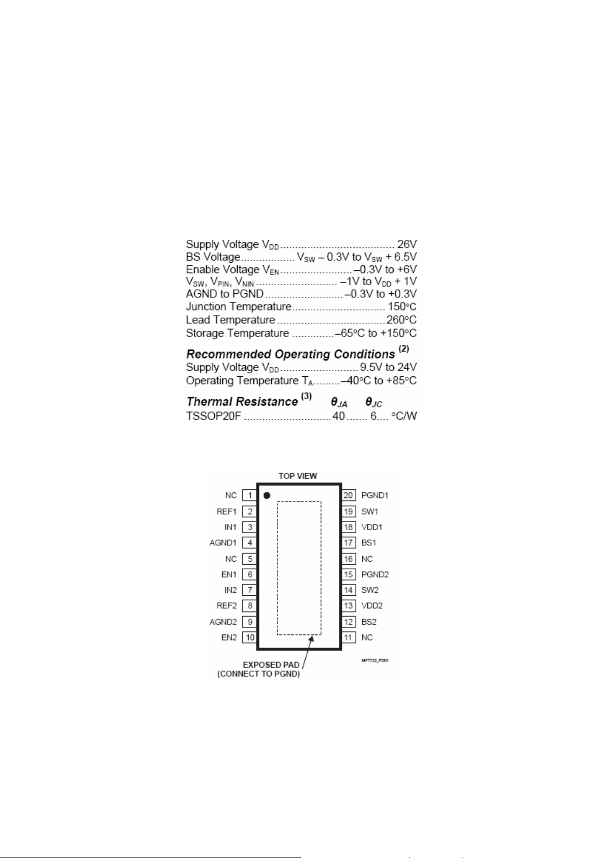
3. AUDIO AMPLIFIER STAGE WITH MP7722
3.1 General Description
The MP7722 is a stereo 20W Class D Audio amplifier, intended for use as low
frequency power amplifier in a wide range of applications in radio and TV sets.
It uses a minimum number of external components to complete a stereo Class D audio
amplifier.
3.2 Features
x 2 x 20W Output at VDD = 24V into a 4 load
x THD+N = 0.06% at 1W, 8
x 93% Efficiency at 20W
x Low Noise (190μV Typical)
x Switching Frequency Up to 1MHz
x 9.5V to 24V Operation from a Single Supply
x Integrated Startup and Shutdown Pop Elimination Circuit
x Thermal and Short Circuit Protection
x Integrated 180m Switches
x Mute/Standby Modes (Sleep)
x Thermally Enhanced 20-Pin TSSOP Package with Exposed Pad
Page 4
3.3 Applications
x Surround Sound DVD Systems
x Televisions
x Flat Panel Monitors
x Multimedia Computers
x Home Stereo Systems
3.4 Absolute Ratings
3.5 Pinning
4. POWER STAGE
The DC voltages required at various parts of the chassis and inverters are provided by a
main power supply unit and power interface board. The main power supply unit is
designed for 24V and 12V DC supply. Power stage which is on-chasis generates +24V
for audio amplifier, 1.8V and 3.3V stand by voltage and 8V, 12V, 5V and 3.3Vsupplies
for other different parts of the chassis.
Page 5

5. MICROCONTROLLER (VCTP)
5.1 General Features
The VCT 6wxyP is dedicated to high-quality FPD and double-scan TV sets. The VCT
6wxyP family is based on functional blocks contained and approved in existing products
like VCT 49xxI, VSP 94x5B, and DPS 94xxA.
Each member of the family contains the entire audio, video, up-conversion processing
for 4:3 and 16:9 50/
60 Hz progressive or 100/120 Hz interlaced stereo TV sets and the control/data
interface for flat-panel displays. The integrated microcontroller is supported by a
powerful OSD and graphics generator with integrated teletext acquisition.
Controller:
x High-performance 8-bit microcontroller, 8051 compatible
x Up to 512 kByte in system program Flash
x WST, PDC, VPS, and WSS acquisition
x Closed caption and V-chip acquisition
x Up to 10 page on chip teletext memory
x Up to 1000 pages with internal memory
x Up to 30 GPIO
Audio:
x Multistandard TV-sound demodulation:
-All A2/NICAM standards
-BTSC/SAP with DBX
-EIA-J
x Baseband sound processing for loudspeaker channel:
-Volume, bass, treble, loudness, balance
-Spatial effect (e.g. pseudo stereo)
-Micronas AROUND
(Virtual Dolby Surround optional)
-Micronas BASS
-BBE
-SRS WOW
-SRS TruSurround XT
-Lipsync function
Video:
x CVBS, S-VHS, YCrCb and RGB inputs
x HDTV YPrPb and RGB inputs
x ITU656 input
x Linedoubling with vertical detail enhancement (without internal memory)
x State of the art motion adaptive up conversion (with internal memory)
x 4H adaptive comb filter for PAL/NTSC (without internal memory)
x 3D comb filter for PAL/NTSC (with internal memory) (Optional)
x Internal SDR RAM interface
x Powerful horizontal and vertical scaling inclusive
x Nonlinear horizontal scaling “panorama vision”
x picture adaptive image improvements (DCE, LSE, CTI, SCE, NCE)
Page 6

x non-linear colorspace enhancement (NCE) with 32 programmable slopes and
sections per RGB component (blue stretch, static black stretch, gamma
correction).
x Dynamic contrast enhancement (DCE) (histogram based black stretch with peak
black and activity detection and contrast adaption)
x Luma sharpness enhancement (LSE)
x Colour transient improvement (CTI)
x Selective colour enhancement (SCE) for skin tone correction, blue and green
stretch
5.2 Multistandard Sound Processor (MSP) Features
The MSP receives the analog Sound IF signal from the tuner and converts it to digital
with its internal SIF-AD converter. The MSP is able to demodulate all TV sound
standards worldwide including the digital NICAM system. TV stereo sound standards
that are unavailable for a specific VCTP version are processed in analog mono sound of
the standard. In that case, stereo or bilingual processing will not be possible.
x Sound IF input
x Worldwide FM/AM-mono sound demodulation
x FM stereo sound demodulation (A2, EIA-J)
x BTSC/SAP demodulation with DBX
x NICAM demodulation
x FM radio & RDS/RBDS demodulation
x Automatic standard detection
x automatic volume correction (AVC)
x Automatic sound select
x Baseband processing for loudspeaker channel:
volume, bass, treble, loudness, balance
-spatial effect (e.g. pseudo stereo)
-Micronas AROUND
-Micronas BASS
-SRS WOW (optional)
-SRS TruSurround XT (optional)
-delayline for lipsync function (shared memory)
-Virtual Dolby Surround (optional)
x 1 I2S input for external ATSC/DVD decoder
x 1 I2S interface for audio delayline
x 1 SPDIF output
x Audio i/o switches
-4 analog stereo line inputs and 2 analog stereo line outputs (configurable 5
analog stereo line inputs and 1 analog stereo line output)
-1 analog stereo loudspeaker output
-1 analog subwoofer output
-1 analog stereo headphone output
5.3 Video Features
The TVT is a Teletext decoder for decoding World System Teletext data, as well as
Video Programming System (VPS), Program Delivery Control (PDC), and Wide-Screen
Signalling (WSS) data used for PALplus transmissions (line 23). The device also
supports Closed Caption acquisition and decoding.
Page 7

The TVT provides an integrated general-purpose, fully 8051-compatible microcontroller
with television-specific hardware features. The microcontroller has been enhanced to
provide powerful features such as memory banking, data pointer, additional interrupts,
shared memory access etc.
The TVT has an internal XRAM of 32 KB and a BOOT ROM of 4 KB. For operation the
code is fetched from a 16bit FLASH, which can be addressed up to 1 MByte.
The controller with dedicated hardware does most of the internal TTX acquisition
processing, transfers data to/from external memory interface, and receives/transmits
data via I2C-bus interface. In combination with dedicated hardware, the slicer stores
TTX data in a VBI buffer of 1 KB. The microcontroller firmware performs all the
acquisition tasks (hamming and parity checks, page search, and evaluation of header
control bits) once per field. Additionally, the firmware can provide high-end Teletext
features like Packet-26 handling, FLOF/TOP and list-pages. The interface-to-user
software is optimised for minimal overhead. TVT is realised in deep submicron
technology with 1.8 V supply voltage and 3.3 V I/O (TTL compatible).
x 16 analog video inputs (4xCVBS/Y/C + 3xRGB/YCrCb/YPrPb)
x Video input switch matrix
x 3 analog video outputs (integrated Y+C adder)
x 24-bit RGB/H/V/clk input (e.g. ext. DVI decoder) or 656 8bit input
x 656 8bit input/output (e. g. for external high-end up conversion by FRCA)
x Multi-standard color decoder PAL/NTSC/SECAM including all substandards
x 2D adaptive comb filter for PAL/NTSC with vertical peaking
x 3D-comb filter for PAL/NTSC (Optional)
x Macrovision compliant multi-standard sync processing
x Trilevel sync slicer for HDTV
x Macrovision detection
x High-quality soft mixer controlled by Fast Blank (alpha blending)
x Fastblank monitor via I2C
x Noise measurement
x Letterbox detection (auto-wide)
x Split screen (OSD and video side by side) and AV PIP
5.4 Controller Features
The TVT is a Teletext decoder for decoding World System Teletext data, as well as
Video Programming System (VPS), Program Delivery Control (PDC), and Wide-Screen
Signalling (WSS) data used for PALplus transmissions (line 23). The device also
supports Closed Caption acquisition and decoding.
The TVT provides an integrated general-purpose, fully 8051-compatible microcontroller
with television-specific hardware features. The microcontroller has been enhanced to
provide powerful features such as memory banking, data pointer, additional interrupts,
shared memory access etc.
x High performance 8-bit microcontroller, 8051 instruction set compatible
x 81 MHz system clock, two machine cycles per instruction
x On-chip debug support (OCDS)
x Up to 512 kByte in system program Flash
x 256 byte on-chip program RAM
x 128 byte on-chip extended stack RAM
Page 8

x 4-level, 24-input interrupt controller
x Patch module for 16 ROM locations
x Two 16-bit reloadable timers
x Capture compare timer for infrared decoding
x Watchdog timer
x Uart
x Real time clock
x PWM units (2 channels 14-bit, 6 channels 8-bit)
x 8-bit ADC (4 channels)
x I2C bus master/slave interface
x Up to 32 programmable I/O ports
5.5 OSD and Teletext Features
The on-chip display unit for displaying Level 1.5 Teletext data can also be used for
customer-defined onscreen displays.
The TVT has an internal XRAM of 32 KB and a BOOT ROM of 4 KB. For operation the
code is fetched from a 16bit FLASH, which can be addressed up to 1 MByte.
In combination with dedicated hardware, the slicer stores TTX data in a VBI buffer of 1
KB. The microcontroller firmware performs all the acquisition tasks (hamming and parity
checks, page search, and evaluation of header control bits) once per field. Additionally,
the firmware can provide high-end Teletext features like Packet-26 handling, FLOF/TOP
and list-pages. The interface-to-user software is optimised for minimal overhead.
5.6 Port Allocation
Page 9

Page 10
Page 11

Page 12
Page 13
Page 14
Page 15
Page 16

Page 17
6. DRX 3961A
6.1 General Desription
The DSP-based Analog TV IF Demodulator DRX 396xA performs the entire
multistandard Quasi Split Sound (QSS) TV IF processing, AGC, video demodulation,
and generation of the sound IF (SIF), requiring only one SAW filter. The IC is designed
for applications in TV sets, VCRs, PC cards, and TV tuners.
The alignment-free DRX 396xA does not need special external components. All control
functions and status registers are accessible via I2C bus interface.
6.2 Features
x Multistandard QSS IF processing with a single SAW
x Highly reduced amount of external components (no tank circuit, no
potentiometers, no SAW switching)
Page 18

x Programmable IF frequency (38.9 MHz, 45.75 MHz, 32.9 MHz, 58.75 MHz,
36.125 MHz etc.)
x Digital IF processing for the following standards: B/G, D/K, I, L/L’, and M/N
x Standard specific digital post filtering
x Standard specific digital video/audio splitting
x Standard specific digital picture carrier recovery:
-Alignment-free
-Quartz-stable and accurate
-Stable frequency lock at 100% modulation and overmodulation up to
150%
-Quartz-accurate AFC information
x Programmable standard specific digital group delay equalization
x Automatically frequency-adjusted Nyquist slope, therefore optimum picture and
sound performance over complete lock in frequency range
x Standard-specific digital AGC and delayed tuner AGC with programmable tuner
take-over point
x Fast AGC due to linear structure
x Adaptive back porch control, therefore fast positive modulation AGC
x No sound traps needed at video output
x SIF output with standard-dependent pre-filtering and amplitude-controlled output
level
x Optimal sound SNR due to carrier recovery without quadrature distortions
x FM radio capability without external components and with standard TV tuner
x Prepared for digital TV (DVB-C, DVB-T, ATSC)
x I2C bus interface
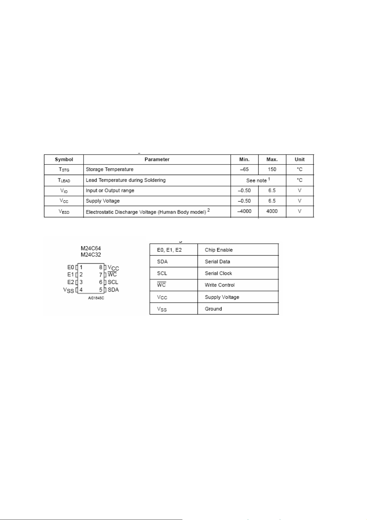
7. SERIAL 64K I2C EEPROM M24C64WBN6
7.1 General Description
M24C64WBN6 is a 64 Kbit Electrically Erasable PROM. These I2C-compatible
electrically erasable programmable memory (EEPROM) devices are organized as
8192x8 bits. It supports 400kHz Protocol I2C uses a two-wire serial interface,
comprising a bi-directional data line and a clock line.
The M24C64WBN6 is available in the standard 8-pin (Vcc, WC, SDA (I2C data), SCL
(I2C clock), Vss,E0,E1,E2). WC pin is critcal pin. If WP is high, writing is not possible to
EEPROM. If WP is low, writing is possible to EEPROM.
7.2 Features
x Two-Wire I2C Serial Interface Supports 400kHz Protocol
x Single Supply Voltage:
– 4.5 to 5.5V for M24Cxx
– 2.5 to 5.5V for M24Cxx-W
– 1.8 to 5.5V for M24Cxx-R
x Write Control Input
x BYTE and PAGE WRITE (up to 32 Bytes)
Page 19
x RANDOM and SEQUENTIAL READ Modes
x Self-Timed Programming Cycle
x Automatic Address Incrementing
x Enhanced ESD/Latch-Up Protection
x More than 1 Million Erase/Write Cycles
x More than 40-Year Data Retention
7.3 Absolute Maximum Ratings
7.4 Pinning
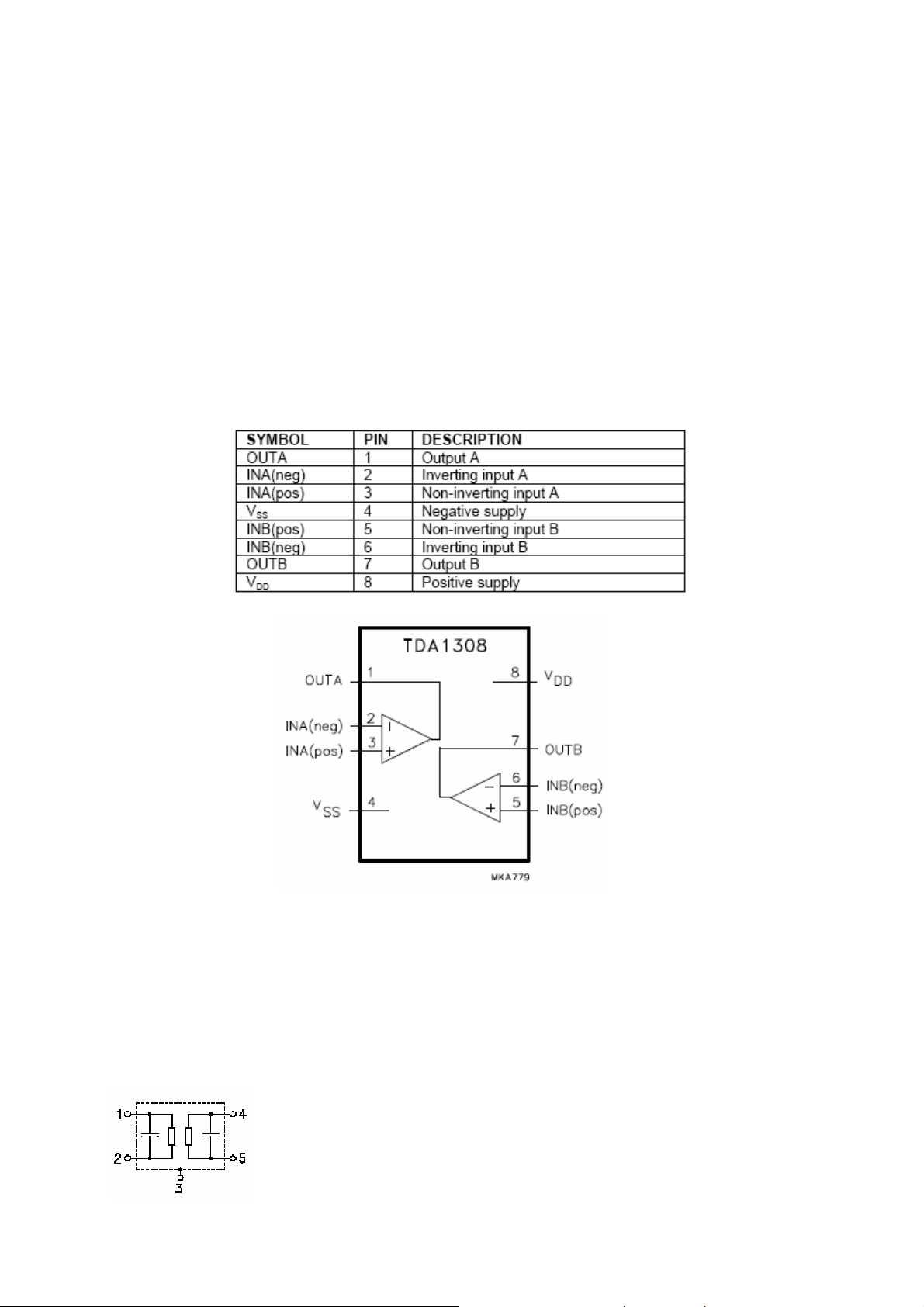
8. CLASS AB STEREO HEADPHONE DRIVER TDA1308
8.1. General Description
The TDA1308 is an integrated class AB stereo headphone driver contained in an SO8
or a DIP8 plastic package. The device is fabricated in a 1 mm CMOS process and has
been primarily developed for portable digital audio applications. It gets its input from two
analog audio outputs (DACA_L and DACA_R) of MSP 34x0G. The gain of the output is
adjustable by the feedback resistor between the inputs and outputs.
8.2 Features
x Wide temperature range
x No switch ON/OFF clicks
x Excellent power supply ripple rejection
x Low power consumption
x Short-circuit resistant
x High performance
x High signal-to-noise ratio
Page 20
x High slew rate
x Low distortion
x Large output voltage swing.
x Power supply maximum 60 mW to 32 (THD<0.1%)
x 5V single supply
x SNR 110 dB
x Power supply ripple rejection
x Typically 3 mA supply current at no load
8.3. Pinning
9. SAW FILTER X6966M
9.1 Features:
- IF filter for digital cable TV
- Plastic package SIP5K
Page 21
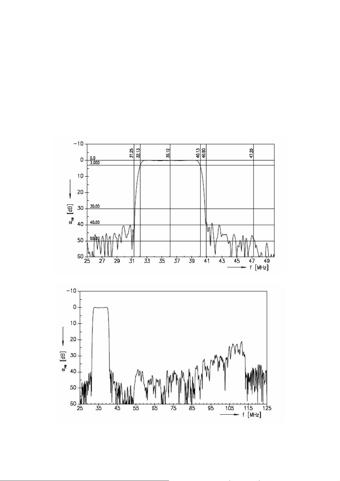
9.2 Pin configuration:
1 Input
2 Input - ground
3 Chip carrier - ground
4 Output
5 Output
9.3 Frequency response:
Page 22

10. IC DESCRIPTIONS AND INTERNAL BLOCK DIAGRAM
LM1117
LM1086
MP1593
FDC642P
SIL9011
24LC02
μPA672T
M74HC4052
Max809
24LC21
10.1. LM1117
10.1.1. General Description
The LM1117 is a series of low dropout voltage regulators with a dropout of 1.2V at
800mA of load current. It has the same pin-out as National Semiconductor’s industry
standard LM317. The LM1117 is available in an adjustable version, which can set the
output voltage from 1.25V to 13.8V with only two external resistors. In addition, it is also
available in five fixed voltages, 1.8V, 2.5V, 2.85V, 3.3V, and 5V. The LM1117 offers
current limiting and thermal shutdown. Its circuit includes a zener trimmed bandgap
reference to as-sure output voltage accuracy to within ±1%. The LM1117 series is
available in SOT- 223, TO-220, and TO-252 D-PAK packages. A minimum of 10μF
tantalum capacitor is required at the output to improve the transient response and
stability.
10.1.2. Features
x Available in 1.8V, 2.5V, 2.85V, 3.3V, 5V, and Adjustable Versions
x Space Saving SOT-223 Package
x Current Limiting and Thermal Protection
x Output Current 800mA
x Line Regulation 0.2% (Max)
x Load Regulation 0.4% (Max)
x Temperature Range
x LM1117 0°C to 125°C
x LM1117I -40°C to 125°C
10.1.3. Applications
x 2.85V Model for SCSI-2 Active Termination
x Post Regulator for Switching DC/DC Converter
x High Efficiency Linear Regulators 15
x 32” TFT TV Service Manual
x Battery Charger
x Battery Powered Instrumentation
Page 23

10.1.4. Absolute Maximum Ratings
10.1.5. Pinning
10.2. LM1086
10.2.1. General Description
The LM1086 is a low dropout three terminal regulator with 1.5A output current capability.
The output voltage is adjustable with the use of a resistor divider. Dropout is guaranteed
at a maximum of 500 mV at maximum output current. It's low dropout voltage and fast
transient response make it ideal for low voltage microprocessor applications. Internal
current and thermal limiting provides protection against any overload condition
that would create excessive junction temperature.
10.2.2. Features
x Low Dropout Voltage 500mV at 1.5A Output Current
x Fast Transient Response
x 0.015% Line Regulation
x 0.1% Load Regulation
x Current Limiting and Thermal Protecion.
x Adjustable or Fixed Output Voltage(1.8, 2.5, 2.85, 3.0, 3.3, 3.45, 5.0V)
x Surface Mount Package SOT-223 & TO-263 (D2 Package)
x 100% Thermal Limit Burn-in
10.2.3. Applications
x Battery Charger
Adjustable Power Supplies
x
Constant Current Regulators
x
Portable Instrumentation
x
High Efficiency Linear Power Supplies
x
Page 24

x High Efficiency "Green" Computer Systems
SMPS Post-Regulator
x
Power PC Supplies
x
x Powering VGA & Sound Card
10.2.4. Absolute Maximum Ratings
10.2.5. Pinning
10.3. MP1593
10.3.1. General Description
The MP1593 is a step-down regulator with an internal Power MOSFET. It achieves 3A
continuous output current over a wide input supply range with excellent load and line
regulation. Current mode operation provides fast transient response and eases loop
stabilisation. Fault condition protection includes cycle-by-cycle current limiting and
thermal shutdown. Adjustable soft-start reduces the stress on the input source at turnon. In shutdown mode the regulator draws 20μA of supply current. The MP1593
requires a minimum number of readily available external components to complete a 3A
step down DC to DC converter solution.
Page 25

10.3.2. Features
x 3A Output Current
x Programmable Soft-Start
x 100mȍ Internal Power MOSFET Switch
x Stable with Low ESR Output Ceramic Capacitors
x Up to 95% Efficiency
x 20μA Shutdown Mode
x Fixed 385KHz Frequency
x Thermal Shutdown
x Cycle-by-Cycle Over Current Protection
x Wide 4.75 to 28V Operating Input Range
x Output Adjustable from 1.22V
x Under Voltage Lockout
x Available in 8-Pin SOIC Package
10.3.3. Applications
x Distributed Power Systems
x Battery Chargers
x Pre-Regulator for Linear Regulators
x Flat Panel TVs
x Set-Top Boxes
x Cigarette Lighter Powered Devices
x DVD/PVR Devices
10.3.4. Absolute Maximum Ratings
Page 26

10.3.5. Electrical Characteristics
10.3.6. Pinning
Pin1:BS
High-Side Gate Drive Boost Input. BS supplies the drive for the high-side N-Channel
MOSFET switch. Connect a 10nF or greater capacitor from SW to BS to power the high
side switch.
Pin2:IN
Power Input. IN supplies the power to the IC, as well as the step-down converter
switches. Drive IN with a 4.75V to 28V power source. Bypass IN to GND with a suitably
large capacitor to eliminate noise on the input to the IC.
Pin3:SW
Power Switching Output. SW is the switching node that supplies power to the output.
Connect the output LC filter from SW to the output load. Note that a capacitor is required
from SW to BS to power the high-side switch
Pin4:GND
Ground.
Pin5:FB
Feedback Input. FB senses the output voltage to regulate that voltage. Drive FB with a
resistive voltage divider from the output voltage. The feedback threshold is 1.222V.
Pin6:COMP
Compensation Node. COMP is used to compensate the regulation control loop. Connect
a series RC network from COMP to GND to compensate the regulation control loop. In
some cases, an additional capacitor from COMP to GND is required.
Pin7:EN
Enable Input. EN is a digital input that turns the regulator on or off. Drive EN high to turn
on the regulator, drive EN low to turn it off. An Under Voltage Lockout (UVLO) function
can be implemented by the addition of a resistor divider from VIN to GND. For complete
low current shutdown its needs to be less than 0.7V. For automatic startup, leave EN
unconnected.
Pin8:SS
.
Page 27

Soft-Start Control Input. SS controls the soft-start period. Connect a capacitor from SS
to GND to set the soft-start period. A 0.1μF capacitor sets the soft-start period to 10ms.
To disable the soft-start feature, leave SS unconnected.
10.4. FDC642P
10.4.1. General Description
This p-channel 2.5V specified MOSFET is produced using Fairchild’s advanced
PowerTrench process that has been especially tailored to minimize on state resistance
and yet maintain low gate charge for superior switching performance.
10.4.2 . Features
10.4.3. Absolute Maximum Ratings
10.4.4. Pinning
Page 28

10.5. SIL9011
The Sil 9011 is a third generation HDMI receiver compatible with the HDMI 1.1 specification.
Backwards compatibility with DVI 1.0 allows HDMI systems to connect to existing DVI 1.0
hosts over a single cable.
The Sil 9011 is capable of receiving and outputting 2 to 8 channels of digital audio of up to
192kHz. An industry-standard I
S/PDIF port supports up to 96kHz audio.
Silicon Image’s HDMI receivers use the latest generation of PanelLink TMDS core technology.
These PanelLink cores pass all HDMI compliance tests.
10.5.1 Features
x HDMI 1.1, HDCP 1.1 and DVI 1.0 compliant receiver
x Integrated PanelLink core supports:
DTV resolutions (480i/576i/480p/576p/720p/1080i)
PC resolutions (VGA, SVGA, XGA, SXGA, UXGA) up to 165MHz.
x Digital video interface supports video processors:
24-bit and 48-bit RGB/ YCbCr 4:4:4
16/20/24-bit YCbCr 4:2:2
8/10/12-bit YCbCr 4:2:2 (ITU BT.656)
x S/PDIF output supports bothIEC 60958 and IEC 67937 for PCM, Dolby Digital,
DTS digital or any S/PDIF type audio transmission (32-96kHz Fs)
2
S port allows direct connection to low-cost audio DACs. An
2
x Four Programmable I
S outputs for connection to low-cost audio DACs.
x Sample rates up to 192kHz
x Auto audio error detection with programmable soft mute.
x Integrated HDCP decryption engine for receiving protected audio and video
content
x Pre-programmed HDCP keys provide highest level of key security, simplifies
manufacturing
10.6. 24LC02
10.6.1. General Description
24AA02/24LC02B (24XX02*) is a 2 Kbit Electrically Erasable PROM. The device is
organized as one block of 256 x 8-bit memory with a 2-wire serial interface. Low-voltage
design permits operation down to 1.8V, with standby and active currents of only 1μA
and 1mA, respectively. The 24XX02 also has a page write capability for up to 8 bytes of
data.
10.6.2 Features
x Single supply with operation down to 1.8V
x Low-power CMOS technology
-1mA active current typical
-1μA standby current typical (I-temp)
Page 29

x Organized as 1 block of 256 bytes (1 x 256 x 8)
x 2-wire serial interface bus, I
2
C™ compatible
x Schmitt Trigger inputs for noise suppression
x Output slope control to eliminate ground bounce
x 100 kHz (24AA02) and 400 kHz (24LC02B) compatibility
x Self-timed write cycle (including auto-erase)
x Page write buffer for up to 8 bytes
x 2ms typical write cycle time for page write
x Hardware write-protect for entire memory
x Can be operated as a serial ROM
x Factory programming (QTP) available
x ESD protection > 4,000V
x 1,000,000 erase/write cycles
x Data retention > 200 years
x 8-lead PDIP, SOIC, TSSOP and MSOP packages
x 5-lead SOT-23 package
x Pb-free finish available
x Available for extended temperature ranges:
-Industrial (I): -40°C to +85°C
-Automotive (E): -40°C to +125°C
10.6.3 Pinning
10.7. μPA672T
10.7.1. General Description
N-channel Mos-Fet array for switching.The μPA672T is a super-mini-mold device
provided with two MOS FET elements. It achieves high-density mounting and saves
mounting costs.
Page 30

10.7.2. Features
x Two MOS FET circuits in package the same size as SC-70
x Automatic mounting supported
10.7.3 Absolute Maximum Ratings
10.7.4 Pinning
10.8. M74HC4052
10.8.1. General Description
The M74HC4052 is a dual four-channel analog MULTIPLEXER/DEMULTIPLEXER
fabricated with silicon gate C2MOS technology and it is pin to pin compatible with the
equivalent metal gate CMOS4000B series. It contains 8 bidirectional and digitally
controlled analog switches.
10.8.2. Features
x LOW POWER DISSIPATION: ICC = 4mA(MAX.) at TA=25°C
x LOGIC LEVEL TRANSLATION TO ENABLE 5V LOGIC SIGNAL TO
COMMUNICATE
x WITH ±5V ANALOG SIGNAL
x LOW "ON" RESISTANCE:
Page 31

70W TYP. (VCC - VEE = 4.5V)
50W TYP. (VCC - VEE = 9V)
x WIDE ANALOG INPUT VOLTAGE RANGE: ±6V
x FAST SWITCHING:
tpd = 15ns (TYP.) at TA = 25 °C
x LOW CROSSTALK BETWEEN SWITCHES
x HIGH ON/OFF OUTPUT VOLTAGE RATIO
x WIDE OPERATING SUPPLY VOLTAGE RANGE (VCC - VEE) = 2V TO 12V
x LOW SINE WAVE DISTORTION: 0.02% at VCC - VEE = 9V
x HIGH NOISE IMMUNITY: VNIH = VNIL = 28 % VCC (MIN.)
x PIN AND FUNCTION COMPATIBLE WITH 74 SERIES 4052
10.8.3 Absolute Maximum Ratings
10.8.4 Pinning
VEE supply pin is provided for analog input signals. It has an inhibit (INH) input terminal
to disable all the switches when high. For operation as a digital
multiplexer/demultiplexer, VEE is connected to GND.
A and B control inputs select one channel out of four in each section. All inputs are
equipped with protection circuits against static discharge and transient excess voltage.
Page 32

10.9. Max809
10.9.1. General Description
The MAX809 and MAX810 are costíeffective system supervisor circuits designed to
monitor VCC in digital systems and provide a reset signal to the host processor when
necessary. No external components are required.
The reset output is driven active within 10 _sec of VCC falling through the reset voltage
threshold. Reset is aintained active for a timeout period which is trimmed by the factory
after VCC rises above the reset threshold. The MAX810 has an activeíhigh RESET
output while the MAX809 has an activeílow RESET output. Both devices are available
in SOTí23 and SCí70 packages.
10.9.2. Features
x Precision VCC Monitor for 1.5 V, 1.8 V, 2.5 V, 3.0 V, 3.3 V, and 5.0 V Supplies
x Precision Monitoring Voltages from 1.2 V to 4.9 V Available in 100 mV Steps
x Four Guaranteed Minimum PoweríOn Reset Pulse Width Available (1 ms, 20
ms, 100 ms, and 140 ms)
x RESET Output Guaranteed to VCC = 1.0 V.
x Low Supply Current
x Compatible with Hot Plug Applications
x VCC Transient Immunity
x No External Components
x Wide Operating Temperature: í40°C to 105°C
x PbíFree Packages are Available
10.9.3 Absolute Maximum Ratings
Page 33

10.9.4 Pinning
Page 34

10.10. 24LC21
10.10.1. General Description
The 24LC21 is a 1K bit electrically erasable programmable memory (EEPROM), organized by 8
bits.This device can operate in two modes: Transmit Only mode and I2C bidirectional mode.
When powered, the device is in Transmit Only mode with EEPROM data clocked out from the
rising edge of the signal applied on VCLK.
10.10.2. Features
x 1 MILLION ERASE/WRITE CYCLES
x 40 YEARS DATA RETENTION
x 2.5V to 5.5V SINGLE SUPPLY VOLTAGE
x 400k Hz COMPATIBILITY OVER the FULL RANGE of SUPPLY VOLTAGE
x TWO WIRE SERIAL INTERFACE I2C BUS COMPATIBLE
x PAGE WRITE (up to 8 BYTES)
x BYTE, RANDOM and SEQUENTIAL READ MODES
x SELF TIMED PROGRAMMING CYCLE
x AUTOMATIC ADDRESS INCREMENTING
x ENHANCED ESD/LATCH UP PERFORMANCES
10.10.3 Absolute Maximum Ratings
Page 35

10.10.4 Pinning
11.SERVICE MENU SETTINGS
In order to reach service menu,
x First Press “MENU”
x Then press the remote control code, which is “4725”
11.1. Video Setup
x Picture Mute <.....>
If “Yes” selected, “Picture mute” feature is active.
x Blue Screen <.....>
If “Yes” selected, “Blue Background” item is seen in “Feature”
menu.
x YC Delay <...........>
Tuner PAL <.....> Value between -8 to+7
Ext PAL <.....> Value between -8 to+7
SECAM <.....> Value between -8 to+7
NTSC <.....> Value between -8 to+7
x AGC (dB) <.....> Value between 0 to+8
11.2. AudioSetup
x Equaliser <.....>
If “Yes” selected, “Equaliser” item is seen in “Sound” menu.
Page 36

x BBE
x SRS WOW
x Virtual Dolby Surround <.....>
If “Yes” selected, Virtual Dolby Surround feature is seen in “Sound”
menu with selected Virtual Dolby Text.
x Virtual Dolby Text The selected item is seen as Virtual Dolby Srround Text.
3DS
Virtual Dolby
3D Panorama
x AVL <.....>
If “Yes” selected, “AVL” item is seen in “Sound” menu.
x Carrier Mute <.....>
If “Yes” selected, “Carrier mute” feature is active.
x Audio Delay Offset
x Prescale
FM Presc. AVL On <.......> Value between 0 to +127
AM Presc. AVL On <.......> Value between 0 to +127
NICAM Presc. AVL On <.......> Value between 0 to +127
I2S Presc. AVL On <.......> Value between 0 to +127
SCART Presc. AVL On <.......> Value between 0 to +127
FM Presc. AVL Off <.......> Value between 0 to +127
AM Presc. AVL Off <.......> Value between 0 to +127
NICAM Presc. AVL Off <.......> Value between 0 to +127
I2S Presc. AVL Off <.......> Value between 0 to +127
SCART Presc. AVL Off <.......> Value between 0 to +127
x Dynamic Bass <.....>
If “Yes” selected, “Dynamic Bass” item is seen in “Sound” menu.
x Subwoofer <.....>
If “Yes” selected, “Subwoofer” item is seen in “Sound” menu.
11.3. Options 1
x VCTP Version <.......>
Basic+
Basic
x Double Digit <.....>
If “Yes” selected, “Double Digit” button is active for channel
selection.
x TEA6415C Available <.....>
If “Yes” selected, video switch IC is active on hardware.
x TEA642X Available<.....>
If “Yes” selected, audio switch IC is active on hardware.
x Power-Up Mode <.......>
StandBy If selected, TV opens in stand by mode.
L.State If selected, TV opens in Last State mode.
x TV Open Mode <.......>
Source
1st TV
Last TV
Page 37

x Select Languages <.......> “Yes” selected languages are seen as option under
the “Language” item in “Feature” menu
Language Set 1
o German <.......>
o French <.......>
o Spanish <.......>
o Italian <.......>
o Danish <.......>
o Finnish <.......>
o Swedish <.......>
Language Set 2
o Greek <.......>
o Norwegian <.......>
o Dutch <.......>
o Portuguse <.......>
o Polish <.......>
o Turkish <.......>
o Russian <.......>
o Czech <.......>
Language Set 3
o Hungarian <.......>
o Slovak <.......>
o Slovenian <.......>
o Romanian <.......>
o Bulgarian <.......>
o Croatian <.......>
o Serbian <.......>
o Hebrew <.......>
x First APS <.......>
If “Yes” selected, first time TV opens by asking APS.
x APS Volume <.......> value between 0 to+63
Burn In Mode <.......>
x
If “Yes” selected, TV opens with Burn-In mode. This mode is
used in manufacturing.
x APS Test
x HDMI WP <.......>
If “Yes” selected, HDMI EDID ROM is write protected.
11.4. Options 2
x Autostore <.......>
If “Yes” selected, Channel is automatically stored.
x Led Type <.............................>
1 Led 1 Colour
1 Led 2 Colours
2 Led 2 Colours
x PC PIP <.......>
x PC Stand By <.......>
Page 38

11.5. Service Scan/Tuning Setup
x Search for L/L’ <.......>
x Pref. Search Standard <...........>
BG, DK, I
L/L’
M
x Station Ident <.......>
x ATS Delay Time (ms) <.......> Value between 20 to 250
x Color Killer Threshold <.......> Value between 0 to +255
x Tuner Options <.......>
Control Byte <.......> Value between 0 to +255
Low-Mid – Low Byte <.......> Value between 0 to +255
Low-Mid – High Byte <.......> Value between 0 to +255
Mid-High – Low Byte <.......> Value between 0 to +255
Mid-High – High Byte <.......> Value between 0 to +255
BSW1 <.......> Value between 0 to +255
BSW2 <.......> Value between 0 to +255
BSW3 <.......> Value between 0 to +255
11.6. External Source Settings
x DTV <.......>
x DVD <.......>
x Ext 2 S-Video <.......>
x Ext 3 <.......>
x Ext 3 S-Video <.......>
x FAV <.......>
x BAV <.......>
x S-Video <.......>
x HDMI 1 <.......>
x HDMI 2 <.......>
x YPbPr <.......>
x PC <.......>
11.7. Picture Mode
x Sources <.......>
Tuner
CVBS
RGB
SVHS
HDMI
YPbPr
PC
PIP
x Picture Mode <.......>
Dynamic
Natural
Cinema
Page 39

x Colour Temp <.......>
Cool
Normal
Warm
x Contrast <.......> Value between 0 to +63
x Brightness <.......> Value between 0 to +63
x Sharpness <.......> Value between 0 to +15
x Colour <.......> Value between 0 to +63
x Backlight <.......> Value between 0 to +255
x R <.......> Value between -63 to +63
x G <.......> Value between -63 to +63
x B <.......> Value between -63 to +63
11.8. Reset TV-Set
x Initialise NVM from ROM
Press green button to reset the NVM from ROM
Page 40

NO DEFECT APPEARANCE DEFECT IDENTIFICATION AND SOLUTIONS
When the TV is operated for the first time,
1
STANDBY LED lights but the TV switches on
Standby LED does not ligh ever.
2
Standby LED does not light and/or IR receiver
3
does not work.
Picture is available but there is no sound.
4
Sound is available but there is no picture.
5
Neither picture nor sound is available.
6
TV switches on but constantly switches to HDMI
input. While trying to tune a channel, always
7
switches to C05.
No sound from PC or YPbPr.
8
TFT backlight level cannot be controlled, it's level
9
is fixed. Q002, Q003, 1006 or surrounding eqipment can be defective or SMD material can be disintegrated.
TV switches on; however, after a short break, it
10
switches off again by itself.
IC403 E2Epron is plugged empty, after the programming process of the first values has finished, TV will switch on by itself.
Are there 3.3V on IC001's bottomright pin? If no, 3.3V are not drawing in, there can be an error in PW board; underneath VCTP, SMD material can be disintegrated.
Are there 1.8V in IC001 solder area? If no,1.8V are not drawing in; IC001 can be defective or underneath VCTP, SMD material can be disintegrated.
Are there 3.3V on IC406's top left pin? If no, IC406 can be defective.
Are there 1.8V on S719? If no, IC001 can be defective.
Are there 3.3V on S700? If no, there can be an error in PW board.
Are there 5V on pin PL409 5? If no, there can be a problem in PW board or SMD material can be disintegrated.
Are there 24V on the pin, which is indicated as number 1, of PL001 socket. If no, there can be a problem in PW board. L603 can be cold soldering.
PL406 can be cold soldering.
Is there display voltage in Q005's top points? (for LG 12V, for other displays 5V). If no; L007 for LG, L006 for other displays can be unplugged.
Q005 can be defective.
Are there 5V in 7th pin of tuner? If no, IC007 and surrounding equipment can be defective, L101 can be defective.
Are there 33V in 9th pin of tuner? If no, there can be a problem in PW board.
Are there 3.3V in L104 inductor? If no, there can be a problem in PW board.
Are there 12V in pin 8 of the PL003 socket? If no, there can be a problem in PW board.
Q410 and Q411 can be defective.
Are there 10V in the mid pin of IC004? If no, IC004 can be defective.
Are there 8V on L200? If no, there can be a problem in D004, D005, D006 or there could be cold soldering.
Are there 1.8V on S719? If no, IC001 can be defective.
Are there 3.3V on S700? If no, PW board can be defective.
IC702 can be defective.
S705 and S706 can be cold soldering.
IC905 or surronding equipment can be defective.
IC 905 supply voltage may not be drawing in 10V.
When the TV is switched on; there should be displayed voltages as following: 5V on C074, 3.3V on PL004 pin 4, 8V on IC004 mid pin and Q005 top points. If one is missing, TV may shut
down after a short while after it is switched on.
12. TROUBLESHOOTING GUIDE
Page 41

13. BLOCK DIAGRAMS
13.1. General Block Diagram
Page 42

13.2. Power Management
Page 43

13.3. DRX (IF Demodulator) Block Diagram
Page 44

13.4. VCTP
14.4.1. General Block Diagram
Page 45

13.4.2. MSP Block Diagram
Page 46

13.4.3 Video Processor of VCT 6wxyP Block Diagram
Page 47

13.5. TDM1300 HARDWARE DESCRIPTION (IDTV)
Item Description
PCB
MPEG decoder
4-layer
EMMA2LL (NEC)
FLASH
DDRAM
Audio DAC
Video AMP
COFDM
Demodulator
Tuner
VCXO
Buck Regulator
3.3V Regulator
1.8V Regulator
1.5V Regulator
74LVC16244 (x4)
74LVC245
74LVC00
29LV160TE (Spansion, Eon) 2MB
EDD1216AATA ( Elpida, Nanya) 16MB
CS4335 (Crystal)
FMS6145 (Fairchild)
DRX3973D (Micronas)
DTT7103 (Thomson)
DTOS401TH17XA (Samsung)
PI6CX100-27 (Pericom)
MP1593 (MPS)
NCP1117-3.3V (Onsemi)
NCP1117-1.8V (Onsemi)
NCP1117-1.5V (Onsemi)
16-bit buffer with OE (Various)
Octal Bus Transceiver (Various)
NAND Gate (Various)
Page 48

13.5.1 IDTV Module Block Diagram
IF INPUT
CON
SAW Filter
COFDM
DEMOD
VCXO
PROGRAM
CON
(UART)
JTAG
CON
ANALOG AV CON
I2C,UART,4 GPIO, IF AGC
VIDEO
AMP
AUDIO
DAC
EMMA2LL
CPU + MPEG DECODER
NEC
DIGITAL AV CON
BUFFERS &
GATES
POWER
5V
3.3V 1.8V 1.5V
LIN.REGULATOR
S/PDIF
CON
16 MB
DDRAM
2 MB
FLASH
PCMCIA
CON
Page 49

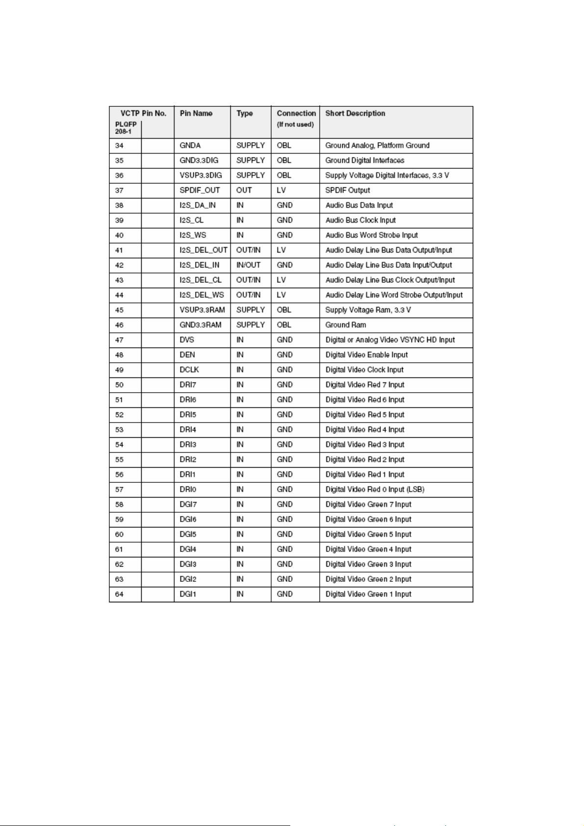
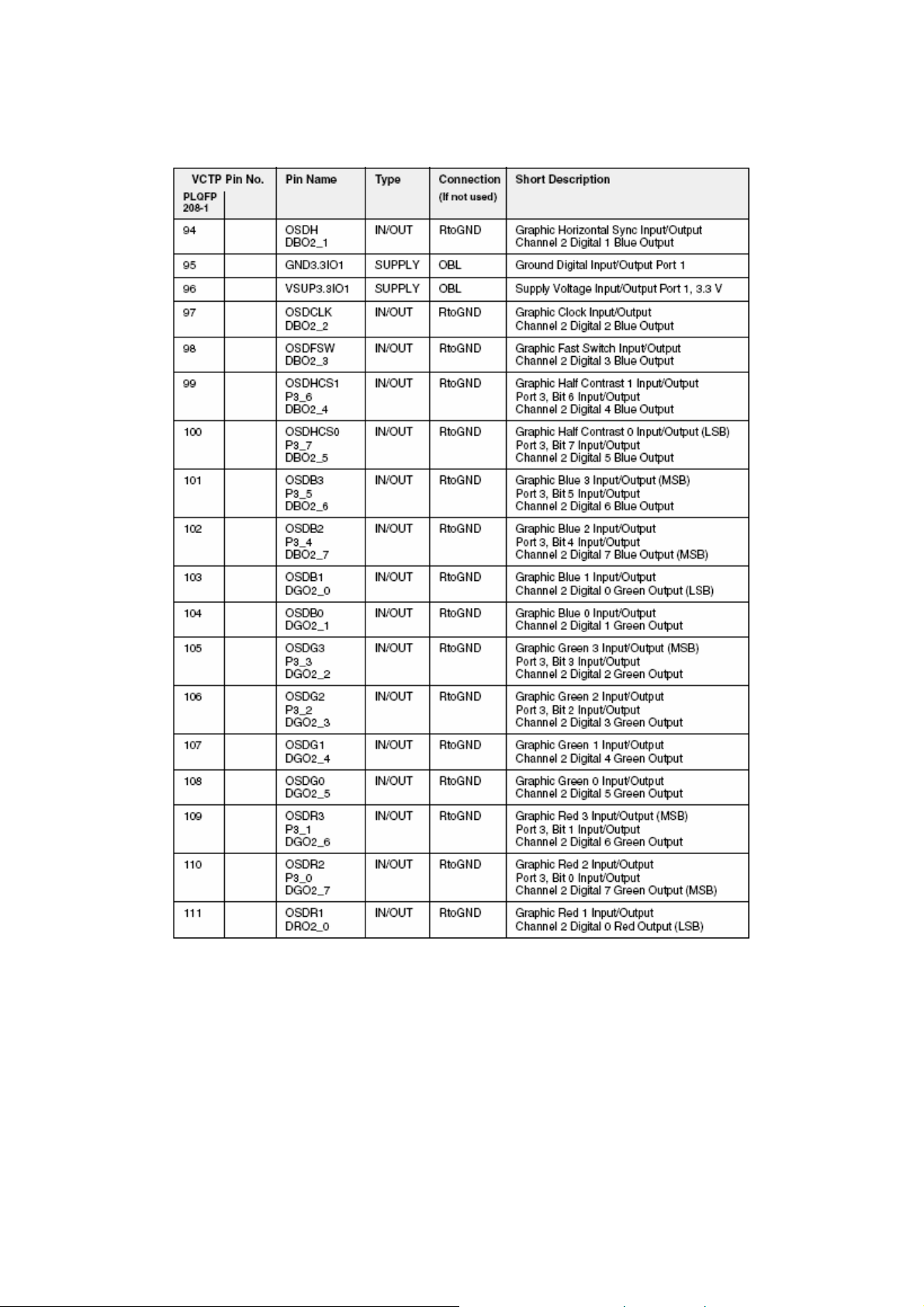
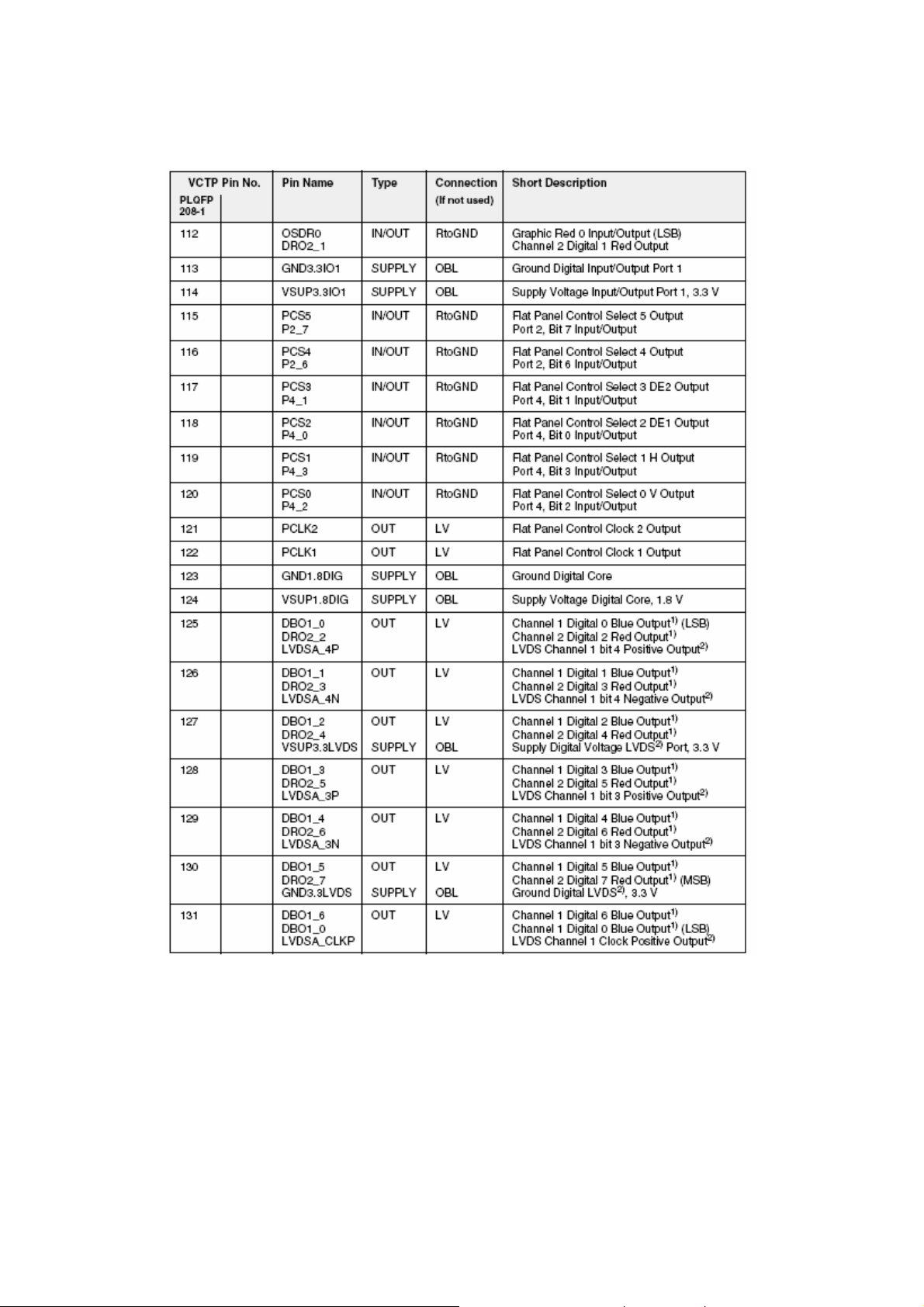
14. CONNECTORS
14.1. POWER Connector
Pin Description
+12/24V
1
+12/24V
2
GND
3
GND
4
14.2. EMMA2LL JTAG Connector
Pin Description
GND
1
JTCLK
2
3.3V
3
JTDO
4
NC
5
JTMS
6
NC
7
JTRST
8
GND
9
JTDI
10
14.3. ANALOG AV Connector
Pin Description Pin Description
DVB_SCL
1
DVB_SDA
2
GND
3
GND
4
IRQ
5
DVB_RX
6
DVB_TX
7
GPIO4
8
GPIO3
9
GPIO2
10
GPIO1
11
IF_AGC_DVB
12
GND
13
GND
14
DVB_R_AUDIO
15
DVB_L_AUDIO
16
GND
17
DVB_IN_CVBS
18
GND
19
DVB_IN_B / DVB_IN_C
20
GND
21
DVB_IN_G / DVB_IN_Y
22
GND
23
DVB_IN_R
24
Page 50

14.4. IF Connector
Pin Description
IF +
1
IF -
2
GND
3
14.5. PROGRAMMING Connector
Pin Description
TXD
1
GND
2
RXD
3
14.6. S/PDIF Connector
Pin Description
S/PDIF
1
GND
2
14.7. DIGITAL AV Connector
Pin Description Pin Description
I2S Word Select
1
I2S Serial Clock
2
I2S Serial Data
3
GND
4
GND
5
GND
6
Internal Vertical SYNC
7
Internal Horizontal SYNC
8
GND
9
GND
10
GND
11
Digital Video Pixel Clock
12
Digital Video Y/Cb/Cr DATA7
13
Digital Video Y/Cb/Cr DATA6
14
Digital Video Y/Cb/Cr DATA5
15
Digital Video Y/Cb/Cr DATA4
16
Digital Video Y/Cb/Cr DATA3
17
Digital Video Y/Cb/Cr DATA2
18
Digital Video Y/Cb/Cr DATA1
19
Digital Video Y/Cb/Cr DATA0
20
Page 51

14.8. PCMCIA Connector
Pin Signal Description Pin Signal Description
GND Ground
1
D3 Data bit 3
2
D4 Data bit 4
3
D5 Data bit 5
4
D6 Data bit 6
5
D7 Data bit 7
6
CE1# Card Enable
7
A10 Address bit 10
8
OE# Output Enable
9
A11 Address bit 11
10
A9 Address bit 9
11
A8 Address bit 8
12
A13 Address bit 13
13
A14 Address bit 14
14
WE# Write Enable
15
IREQ# Interrupt Request
16
VCC Supply Voltage
17
Programming and
VPP
18
MIVAL MPEG Data In Valid
19
MCLKI MPEG Data Clock Input
20
A12 Address bit 12
21
A7 Address bit 7
22
A6 Address bit 6
23
A5 Address bit 5
24
A4 Address bit 4
25
A3 Address bit 3
26
A2 Address bit 2
27
A1 Address bit 1
28
A0 Address bit 0
29
D0 Data bit 0
30
D1 Data bit 1
31
D2 Data bit 2
32
IOIS16# I/O Port Is 16-bit
33
GND Ground
34
Peripheral Supply
GND Ground
35
CD1# Card Detect
36
MDO3 MPEG Data Out 3
37
MDO4 MPEG Data Out 4
38
MDO5 MPEG Data Out 5
39
MDO6 MPEG Data Out 6
40
MDO7 MPEG Data Out 7
41
CE2# Card Enable
42
VS1# Voltage Sense 1
43
IORD# I/O Read
44
IOWR# I/O Write
45
MISTRT MPEG Data In Start
46
MDI0 MPEG Data In 0
47
MDI1 MPEG Data In 1
48
MDI2 MPEG Data In 2
49
MDI3 MPEG Data In 3
50
VCC Supply Voltage
51
Programming and
VPP
52
MDI4 MPEG Data In 4
53
MDI5 MPEG Data In 5
54
MDI6 MPEG Data In 6
55
MDI7 MPEG Data In 7
56
MCLKO MPEG Data Clock Output
57
RESET Card Reset
58
WAIT# Extend bus cycle
59
INPACK# Input Port Acknowledge
60
REG#
61
MOVAL MPEG Data Out Valid
62
MOSTRT MPEG Data Out Start
63
MDO0 MPEG Data Out 0
64
MDO1 MPEG Data Out 1
65
MDO2 MPEG Data Out 2
66
CD2# Card Detect
67
GND Ground
68
Peripheral Supply
Register select & I/O
Enable
Page 52

15. CONCEPT ICs
15.1. μPD61115
15.1.1 Description
The μPD61115 device is a member of the second generation of multimedia processors based on NEC’s
Enhanced MultiMedia Architecture (EMMArchitecture). These devices provide nearly all the functionality
required to realise a high performance and cost-effective digital set-top box or integrated digital TV.
15.1.2 Features
x MPEG1 and MPEG2-TS/PS compliant
x High performance MIPS32™ 4Kc™ main CPU core
x High performance MIPS32™ 4Km™ sub-CPU core
x Integrated DVB descrambling with family options for Irdeto and Multi2
x 36 PID filters, 32 section filters
x Video Outputs: 4 DACs for RGB, Component video, S-video and composite output with support
for PAL, NTSC and SECAM
x 4 graphics planes
x Audio Output: 2-channel PCM and SPDIF
x Peripherals support
two fast UARTs with 16byte FIFOs
I
2C interface
infrared receiver
three wire clocked serial interface
x System timers, RTC and Watchdog timer
x Motorola/Intel Bus.
15.2. DRX 3973D
Fourth-Generation COFDM Demodulators
15.2.1 Introduction
The DRX 3973D and the DRX 3977D are fourth-generation COFDM demodulators that offer today’s
highest level of front-end integration resulting in ultimate DVB-T digital reception, compliant to ETS 300
744, DTG D-Book, EICTA E-Book, and Nordig Unified v1.0.2 .
The DRX 3973/77D applies cutting-edge digital filtering techniques in combination with a highperformance A/D-converter and PLL configuration, resulting in superior performance figures in the
presence of digitaland analog adjacent channels.
Progressive channel estimator algorithms provide exceptional performance in multipath- and dynamicecho
conditions – an especially important feature for single-frequency networks and indoor reception.
The state-of-the-art impulsive noise cruncher suppresses interferences originating from sources such as
cars, electrical motors, and household appliances.
Page 53

15.2.2 Features
Highest level of front-end integration and flexibility:
Integrated PGA (programmable gain amplifier) 30 dB
Single 8 MHz SAW filter operation
2 AGC control signals available for RF and IF amplifier control
Flexible clock reference options
Re-use of 4 MHz tuner clock reference
Pre-SAW sense input for optimal RF AGC setting and RF-level measurement
Excellent digital reception performance:
Superior digital and analog adjacent channel performance (> 40dB for QEF)
Impulsive noise cruncher
Multipath and dynamic echoes
The input IF frequency ranging up to 44 MHz ensures upward compatibility for new tuner topologies
Integrated microprocessor to perform autonomous detection and operation of all possible DVB-T
modes, without interaction with the host processor
Fully automatic and fast signal acquisition: UHF and VHF band-scan in <20 seconds
Meets all international DVB-T receiver specifications: Nordig Unified, DTG, EICTA
Comfortable software drivers for integration of tuner and COFDM demodulator
Secondary serial interface for tuner control
5 V tolerant AGC and secondary serial protocol outputs
2 general purpose I/O pins (GPIO)
Configurable parallel or serial MPEG-TS output
PMQFP64-2 package: footprint 1010 mm (DRX 3973D)
PQFN48-1 package: small footprint 77 mm (DRX 3977D)
IEEE 1149.1 boundary scan
15.2.3 Applications
IDTV / hybrid TV
Set-top boxes
PVR / DVDR
Network interface modules (NIM)
PC-TV applications
15.3. PI6CX100-27
27 MHz 3.3V VCXO for Set-Top Box Applications
15.3.1 Features
• 3.3V operating voltage
• Uses an inexpensive external crystal
• On-chip VCXO with pull range of 240ppm
• VCXO tuning voltage from 0 to 3.3V
• 10mA output drive at CMOS levels
• Available in SOIC package
Page 54

15.3.2 Description
The PI6CX100-27 is a low-cost, high-performance 3.3V VCXO, designed to replace expensive VCXO
modules. The on-chip Voltage Controlled Crystal Oscillator accepts a 0 to 3.3V input voltage to cause
clocks to vary by ±120ppm. This device uses an inexpensive external pullable crystal at 27 MHz to
produce the same output frequency.The PI6CX100-27 is designed for Set-Top Box applications.
15.4. 74V1G08
SINGLE 2-INPUT AND GATE
HIGHSPEED: tPD = 4.3 ns (TYP.) atVCC= 5V
LOWPOWERDISSIPATION:
I
CC =1 PA (MAX.) at TA =25 oC
HIGHNOISEIMMUNITY:
V
NIH=VNIL =28%VCC (MIN.)
POWERDOWN PROTECTIONON INPUTS
SYMMETRICAL OUTPUT IMPEDANCE:
|I
OH| = IOL = 8 mA(MIN)
BALANCEDPROPAGATIONDELAYS:
tPLH #tPHL
OPERATINGVOLTAGERANGE:
V
CC (OPR)= 2V to 5.5V
IMPROVEDLATCH-UP IMMUNITY
16.4.1 Description
The 74V1G08 is an advanced high-speed CMOS SINGLE 2-INPUT AND GATE fabricated with submicron silicon gate and double-layer metal wiring C
2MOS technology.
15.5. FMS6145
Low Cost Five Channel 4th Order Standard Definition Video Filter Driver
15.5.1 Features
x Five fourth-order 8MHz (SD) filters
x Transparent input clamping
x Dual video load drive (2Vpp, 75)
x AC or DC-coupled inputs
x AC or DC-coupled outputs
x DC-coupled outputs eliminate AC-coupling capacitors
x 5V only
x Lead (Pb) Free TSSOP-14 package
Page 55

15.5.2 Applications
x Cable set top boxes
x Satellite set top boxes
x DVD players
x HDTV
x Personal video recorders (PVR)
x Video on demand (VOD)
15.5.3 Description
The FMS6145 Low Cost Video Filter (LCVF) is intended to replace passive LC filters and drivers with a
low-cost integrated device. Five 4th order filters provide improved image Quality compared to typical 2nd
or 3rd order passive solutions.
The FMS6145 may be directly driven by a DC-coupled DAC output or an AC-coupled signal. Internal
diode clamps and bias circuitry
may be used if AC-coupled inputs are required.
The outputs can drive AC or DC-coupled single (150) or dual(75) loads. DC-coupling the outputs
removes the need for output coupling capacitors. The input DC levels will be offset approximately +280mV
at the output.
15.6. MP1593
3A, 28V Step-Down Converter
15.6.1 Description
The MP1593 is a step-down regulator with an internal Power MOSFET. It achieves 3A
continuous output current over a wide input supply range with excellent load and line regulation.
Current mode operation provides fast transient response and eases loop stabilisation. Fault
condition protection includes cycle-by-cycle current limiting and thermal shutdown. Adjustable
soft-start reduces the stress on the input source at turn-on. In shutdown mode the regulator
draws 20μA of supply current.
The MP1593 requires a minimum number of readily available external components to complete
a 3A step down DC to DC converter solution.
15.6.2 Features
x 3A Output Current
x Programmable Soft-Start
x 100m Internal Power MOSFET Switch
x Stable with Low ESR Output Ceramic Capacitors
x Up to 95% Efficiency
x 20μA Shutdown Mode
x Fixed 385KHz Frequency
Page 56

x Thermal Shutdown
x Cycle-by-Cycle Over Current Protection
x Wide 4.75 to 28V Operating Input Range
x Output Adjustable from 1.22Vs
x Under Voltage Lockout
x Available in 8-Pin SOIC Package
15.6.3 Applications
x Distributed Power Systems
x Battery Chargers
x Pre-Regulator for Linear Regulators
x Flat Panel TVs
x Set-Top Boxes
x Cigarette Lighter Powered Devices
x DVD/PVR Devices
Page 57

16. REPLACEMENT PARTS
THE UPDATED PARTS LIST
FOR THIS MODEL IS
AVAILABLE ON ESTA
Page 58

17. ASSEMBLY DRAWING [For 37-inch models ONLY]
25
26
24
21
16
15
17
18
19
13
11
20
23
14
12
10
6
3
2
7
5
4
9
8
No. 0243
22
1
EXPLODED VIEW
Page 59

[For 32-inch models ONLY]
29
28
19
18
31
31
23
22
17
27
17
26
25
24
17
21
20
13
11
12
7
10
15
14
30
16
34
9
6
3
2
8
5
4
33
1
33
No. 0243
EXPLODED VIEW
Page 60

18. SCHEMATIC DIAGRAMS
5V_TUNER
TU100
TECH2949PG40B
R139
3k3
PTC RES
L105
47u
C115
50V
C114
C117
10u
330R_100MHZ_3A
L114
5V_DRX
16V
100n
C116
3V3_DRX
10V
100n
10V
100n
C118
L106
16V
100n
C119
600R_100MHZ_200mA
C120
L113
SHEET3 VCTP PIN80
16V
100n
C141
100n
DRX_CLK
1 AVSS_ADC
2 AVDD_ADC
3 ANATSTX
4 ANATSTY
5 AVDD_FE8
6 AVSS_FE8
7 AVSS_FE401
8 IFINX
9 AVDD_FE40
16V
10 IFINY
11 AVSS_FE402
C121
100n
16V
R138
VCC_5V
VCC_12V
S100
N.C.
C101
1UF 16 V
10n
N.C.
50V
SHORT
1UF 16 V
C100
50V
50V
C102
10n
39p
39p
C103
R100
PTC RES
R101
S103
R102
5k1
R103
5k1
S101
25V
S102
R104
100R
R105
100R
16V
1u
C104
3k3
S113
4k7
1u
L100
1AGC
2TU
3AS
4SCL
5SDA
6NC
7VS
8NC/ADC
9VST
10IF2
11IF1
R140
5k1
AN_IF
5V_TUNER
R106
5k1
N.C.
C107
VCC_5V
100n
IF_AGC
BLM21A601S
L112
10u
25V
25V
100n
100u
100n
C110
10V
16V
S118
C109
100n
C139
50V
47u
47u
5V_TUNER
50V
R107
1k
IF_AGC
5V_TUNER
C111
50V
C138
L116
10u
L102
10u
16V
L101
C108
1n
C140
47k
47k
R127
VCC_33V
R128
12V_IF
R132
12V_IF
Q102
BF799
R136
470R
47R
PL100
DIGITAL IF CONNECTOR
3
2
1
50V
50V
1n
1n
C135
C136
S111
S112
150R
R125
150R
R126
R123
150R
R124
150R
Q103
BF799
R135
47R
R131
12V_IF
470R
S117
S119
R130
R129
X6966M
IN11
IN22
47k
47k
Z100
GND
50V
C137
OUT1 4
OUT2 5
3
VCC_3V3
DRX POWER SUPPLY
1n
5V_DRX
AN_IF
L103
10u
L117
10u
L104
10u
5V_DRX
5V_DRX
47u
50V
3V3_DRX
6k2
R108
1k2
C134
50V
1n
27p
50V
100n
44
SGND
C123
43
VREF
20.25MHz
16V
C122
X100
42
XTALOUT
3V3_DRX
27p
C124
10u
L108
16V
100n
C125
37
38
39
40
41
DVSS_ADC
PORT5
DVDD_ADC
ADR_SEL
XTALIN
IC100
DRX3960A
AVSS_SYN14SHIELD15TEST016TEST117TEST218CVBS19REF_SW20SIF21AVDD_DAC22AVSS_DAC
AVDD_SYN
12
13
S115
L107
S116
6k2
R110
36
PORT4
3V3_DRX
R111
L109
6k2
35
PORT3
6k2
R112
34
PORT2
TUNER_AGC
DVSS_CAP
DVDD_CAP
RESETQ
TEST_EN
C126
100n
16V
SHEET 8
SHEET3
PORT1
PORT0
DVSS
DVDD
SCL
SDA
VGA_MUX_SW
YPBPR_MUX_SW
AUDIO_MUX_SW
SYNC_SW1
33
32
31
30
29
28
27
26
25
24
23
L110
R116
X
X
3_DR
3V3_DRX
_DR
3V
5V
6k2
6k2
6k2
R118
R117
33n
50V
C130
Q101
BC848B
SHEET 3
100n
C132
SCL_3V3_IC
SDA_3V3_IC
SHEET 3,5,6
1k
R121
16V
C133
3V3_DRX
3V3_DRX
R122
470R
16V
100n
RESET_IC
SHEET3
C127
C128
SYNC_SW2
SW_ENABLE2
3V3_DRX
16V
100n
C129
L111
R119
C131
100R
R120
100R
100n
16V
33p
25V
25V
33p
SHEET3
SCL_DVB
SCL_5V_IC
AGC_DVB
IF_AGC
S104
S120
S121
IC101
1 2Y1
2 2Y0
S105
3 3Y1
43Z
5 3Y0
6
E
7 VEE
8 GND 9S3
74HCT4053
5V_DRX
R109
100R
QSS
5V_DRX
16VCC
5V_TUNER
R137
47R
Q100
BC848B
1k
VCC_8V_VIDEO
C142
10u
16V
R113
R114
75R
R115
75R
SHEET 3
TUNER_CVBS_IN
TUNER_CVBS_SW
SHEET 8
152Z
141Z
131Y1
121Y0
11S1
10S2
SDA_DVB
S106
S107
S108
TV/DVB_SWITCH
C112
C113
100n
S109
SDA_5V_IC
TUNER/DRX
DEMODULATOR
Q104
BC848B
R134
4k7
R133
1k
5V_TUNER
S114
SYNC_SW2
5V_TUNER
10V
100n
10V
S110
AGC_TV
17MB22-2
MAIN BOARD CIRCUIT - SHEET 1
Page 61

SHT3
VCTP_AOUT2R
VCTP_AOUT2L
VCC_8V
SC3_AUDIO_L_OUT
C200
R332
47R
SC3_AUDIO_R_OUT
C201
1n
50V
R200
330R
50V1nC203
R201
330R
1n
50V
330R
R203
R204
330R
50V
C202
1n
50V
VCTP_AOUT1R
VCTP_AOUT1L
VCC_3V3
S209
3k3
R321
Q211
BSN20
11
R333
47R
47u
50V
C256
TO SHT3
UART_RX
UART_TX
IRQ
Q213
BSN20
BSN20
Q214
Q212
BSN20
9
10
R285
5
7
8
6
L221
1n
50V
C254
330R
L222
1n
50V
C257
50V
1nC253
330R
R286
1n
50V
C255
1k
R293
R290
BC858B
100R
Q208
R291
100R
C266
SC3_AUDIO_R_OUT
22u
50V
C267
SC1_AUDIO_R_OUT
22u
50V
1k
R295
C268
SC3_AUDIO_L_OUT
22u
50V
BC858B
Q209
C269
SC1_
AUDIO_
L_OUT
22u
50V
TO SHT7
DMP_DVD_R
R326
75R
R327
75R
R328
75R
12
SW_UPDATE_EN
SC2_PIN8
TO SHT1
47R
SDA_DVB
SCL_DVB
1
3
2
4
PL207
L224
PL208
123456789101112131415161718192021
L223
L226
1n
50V
C259
1n
C260
C263
330R
R292
330R
R294
50V
C264
R301
5k6
16V
100n
C265
R298
15k
R302
75R
R297
C270
1n
50V
47R
R299
1n
50V
47R
R300
TV_LINK_3V3
R303
3V3_STBY
3k3
5V_STBY
Q210
D224
C5V6
BSN20
4k7
R309
R304
100R
27p
75R
50V
R305
47R
R306
D225
C5V6
47R
R307
SC3_SVHS_C
27p
75R
50V
R310
C273
R311
D226
C5V6
R312
R324
75R
C274
47R
47R
DMP_DVD_G
DMP_DVD_B
34
56
SC2_FB
47R
R313
47R
R314
27p
D227
TO SHT3
DMP/DVD_SWITCH
78
75R
R325
DMP_DVD_CVBS_IN
TO SHT3
C5V6
D228
R315
75R
50V
C5V6
TO SHT7
DMP_DVD_AUDIO_R_IN
910
1112
1314
DMP_DVD_AUDIO_L_IN
TO SHT7
27p
50V
R318
C277
D229
C5V6
1516
75R
IR_DMP/DVD
1718
50V
47R
R319
47R
R320
TO SHT3
VCC_5V
10u
L235
1920
DMP CON
PL210
47u
C281
27p
50V
C280
D230
C5V6
VCC_8V
47u
50V
C208
R206
100R
R207
100R
C204
1n
50V
L201
C205
1n
50V
L202
1n
50V
C206
L203
L204
1n
C207
50V
C215
C210
50V
1k
R221
BC858B
Q201
C218
330R
22u
50V
1n
C219
22u
50V
SC3_AUDIO_L_IN
C220
1n
50V
330R
R228
C221
1n
50V
L210
75R
R230
R229
R231
C223
330R
1n
C224
C225
100n
16V
15k
C222
47R
50V 27p
D207
C5V6
47R
47R
R235
1k
R218
BC858B
Q200
TO SHT7
SC3_AUDIO_R_IN
C213
1n
50V
330R
R219
C214
1n
50V
L206
L208
424140393837363534333231302928272625242322
PL203
1n
1n
L209
212019181716151413121110987654321
L205
L207
50V
1n
C216
330R
R217
330R
R222
50V
1n
C217
C229
SC2_AUDIO_R_OUT
22u
50V
R232
L211
1n
50V
C227
R233
1n
50V
C228
SC3_PIN8
47R
R237
R243
D209
C5V6
15k
R238
C226
75R
R234
100n
16V
47R
R239
D208
C5V6
5k6
47R
R240
R236
LINE_R_OUT
50V
C231
SC2_AUDIO_L_OUT
22u
50V
L212
LINE_L_OUT
50V
TO SHT3
SC3_SVHS_C
5k6
S200
SC2_R/C ILE PARALEL
C230
C232
27p
27p
75R
R246
R241
50V
50V
47R
R244
D210
D213
C5V6
C5V6
47R
R245
VCC_5V_VIDEO
18k
470R
R269
R259
Q205
BC848B
R273
150R
BC858B
150R
R270
Q202
VOUT2
470R
TO SHT3
VOUT1
TO SHT7
SC3_CVBS_IN
47R
R253
R331
75R
R330
D217
C5V6
C233
27p
50V
D214
C5V6
R248
R249
C235
27p
50V
C234
27p
75R
R250
50V
47R
D215
D216
C5V6
47R
C5V6
75R
47R
R254
R329
75R
75R
R251
C5V6
D218
R261
R256
47R
47R
C236
27p
50V
75R
R252
R267
18k
R260
Q204
BC848B
R271
23
150R
IDTV_G
21
22
SC1_CVBS_IN
150R
R268
TO SHT7
IDTV_B
20
BC858B
Q203
IDTV_R
24
TO SHT3 SHT7 [TO VIDEO SW]
SC3_CVBS_OUT
IDTV_CVBS_IN
R322
19
BC858B
Q207
BC858B
Q206
R274
75R
R275
75R
75R
R323
IDTV_AUDIO_L_IN
75R
17
18
10V
C250
100n
SHT3
R278
75R
SC2_CVBS_OUT
VCC_5V_VIDEO
10V
100n
C249
SC1_CVBS_OUT
S210
AGC_DVB
IF_AGC
IDTV_AUDIO_R_IN
12
13
15
16
14
IDTV_FFC_CON[ANALOG]
3V3_STBY
TO SHT1
SC1_AUDIO_L_IN
SC1_AUDIO_R_IN
TO SHT3
75R
75R
R202
R205
PL200
1
2
3
4
5
6
7
8
9
10
11
12
13
14
15
DSUB_VGA_CONN
PC VIDEO GND TO CHASIS GND
S213
S211
S212
R208
VCC_5V
SC1_B
SC1_PIN8
SC1_AUDIO_L_OUT
SC1_AUDIO_R_OUT
BAV99
D205
BAV99
D203
BAV99
D200
27p
75R
50V
C211
R213
47R
R214
47R
R215
47R
27p
50V
C209
27p
50V
C212
BAV99
DDC_5V
R209
47R
R210
1k
R211
1k
R212
47R
D206
BAV99
D201
3k3
10k
R216
R220
BAV99
D204
BAV99
D202
VCC_5V
R223
47R
R224
47R
R225
47R
PC_R
PC_G
PC_B
TO SHT7
RGB SW
DDC_SDA
R226
47R
PC_HSYNC
TO SHT3
SYNC SW
PC_VSYNC
R227
47R
DDC_SCL
VCC_3V3
SC1_G
TO SHT3
4VSS
5SDA
TO SHT3 VCTP
HP_DETECT
SC1_R
SC1_FB
BAV_CVBS_IN
SC1_CVBS_OUT
2NC2
1NC1
3NC36SCL
FAV_CVBS SVHS_Y PARALEL
R255
PL204
1
2
S201
3
4
5
6
7
IC200
ST24LC21
7VCLK
8VCC
VCC_5V
D219
D212
FAV VIDEO
PL205
8
1
2
3
PC_VSYNC
DDC_5V
D211
C5V6
R242
47R
4
FAV AUDIO
FAV_HP
PL206
C238
1
2
R247
3
4
47R
C240
C239
27p
75R
50V
C237
27p
50V
L215
L216
1n
1n
50V
C243
C241
BAV_R_IN
BAV_L_IN
L218
LINE_R_OUT
L217
1n
50V
L213
L214
1n
50V
LINE_L_OUT
L219
R262
330R
1n
50V
C242
C244
C245
C5V6
D220
R265
47R
330R
R272
R264
330R
1n
50V
C246
1n
C247
1n
50V
HP_OUT_R
HP_OUT_L
1n
50V
50V
50V
C248
TO SHT3
SUBW
R276
47R
FAV_CVBS_IN
FAV_AUDIO_R_IN
1n
50V
TO SHT4
FAV_AUDIO_L_IN
YPBPR_Y
47R
47R
R279
R282
47R
47R
R280
R283
R281
75R
C251
27p
50V
3
12
A
S203
S202
JK200
1P_RED_FAV
YPBPR/LINE_IN[R/L] CVBS JACK
TO SHT3
SC2_AUDIO_R_IN
SC2_AUDIO_L_IN
FAV SVHS/C SC2 RED ILE PARALEL
TO SHT7
TO SHT7
YPBPR_PB
YPBPR_PR
47R
R287
47R
R288
R284
C252
WHITE_FAV
R289
75R
75R
C258
27p
27p
50V
50V
3
12
A
YELLOW_FAV
S204
JK201
JK202
BAV_CVBS_IN
SC2_AUDIO_L_OUT
SC2_AUDIO_R_OUT
VCC_5V
BAV99
D221
BAV99
D222
BAV99
D223
3
12
A
C261
1n
50V
C262
1n
50V
YPBPR_AUDIO_R_IN
330R
R296
L227
3
A
1P_RED_FAV
JK205
SC2_B
BAV_R_IN
S205
12
TO SHT7
L225
YPBPR AUDIO
SC2_G
C271
1n
50V
C272
1n
50V
2
A
WHITE_FAV
JK206
YPBPR_AUDIO_L_IN
330R
R308
BAV_L_IN
L228
S206
31
SHT4
HP_OUT_L
SC2_R/C
HP_OUT_R
S208
S207
C275
50V
C276
50V
SC2_CVBS_OUT
TO SHT3 VCTP
TO SHT7
PC_AUDIO_L_IN
1n
330R
R316
1n
L229
3
JACK-AK16
JK204
PC_AUDIO_R_IN
C278
1n
50V
330R
R317
C279
1n
50V
L230
12
HEADPHONE JACK PC
SC2_CVBS_IN
SCART, VGA,
DMP, IDTV, FAV
CONNECTORS
L231
17MB22-2
MAIN BOARD CIRCUIT - SHEET2
Page 62

PC STANDBY MODE
SYNC DETECTION
R554
PC_HSYNC
PC_VSYNC
EXTERNAL AMP.
VCC_3V3
R400
4k7
3V3_STBY
12345
SHEET 4
HEADPHONE_R
HEADPHONE_L
AMPLIFIER_R
AMPLIFIER_L
R553
10k
10k
R404
SUBW
47k
PL400
AMP_MUTE
IC406
LM809
3V3_STBY
1
Q400
BC848B
Q419
BC848B
R403
10k
23
10k
N.C.
R408
R409
47k
10k
N.C.
R407
VCTP POWER SUPPLIES
L400
3V3_STBY
1n
1kV
C404
C410
L401
3V3_STBY
1n
1kV
C405
C411
L402
3V3_STBY
1n
1kV
C406
C412
L403
3V3_STBY
1n
1kV
C407
C413
3V3_STBY
L404
1n
1kV
100n
C403
C409
L405
1n
1kV
C408
C414
3V3_STBY
R405
R410
47k
100n
100n
100n
100n
16V
100n
47k
3V3_STBY
4k7
R412
R411
47k
SHORT
SHORT
50V
4u7
C418
16V
16V
16V
16V
C416
16V
5V_STBY
10k
R402
Q401
BC848B
R413
10R
SHEET 2
VCC_5V
VSUP_3V3_DAC
VSUP_3V3_FE
1V8_STBY
VSUP_3V3_COM
1V8_STBY
VSUP_3V3_LVDS
VSUP_3V3_DRI_RAM
25V
100n
VSUP_3V3_IO1
100n
C419
R420
10k
Q403
BC848B
VCTP_AOUT2R
VCTP_AOUT2L
VCTP_AOUT1R
VCTP_AOUT1L
R415
10k
R414
VCC_8V
C494
16V
10u
50V
R421
47R
C421
R417
47k
10k
N.C.
R416
47k
N.C.
50R_100MHZ_3A
L406
1n
50V
C495
PL401
16V
470n
SHORT
SHORT
L407
L408
TANTAL CA SE A
L409
3V3_STBY
Q404
BC848B
1516
1314
1112
910
78
56
34
12
SC1_AUDIO_R_IN
SC1_AUDIO_L_IN
SC2_AUDIO_R_IN
SC2_AUDIO_L_IN
SHEET 2
C426
C427
10u
10V
C425
C428
1V8_STBY
KEYBOARD
JTAG CONN.
TDI
VCTP_AIN3R
VCTP_AIN3L
VCTP_AIN4R
VCTP_AIN4L
1n
50V
C436
50V
SHEET 1
VSUP_5V_SIF
1n
16V
1kV
100n
C432
VSUP_8V_AU
1n
16V
1kV
100n
C433
VSUP_1V8_DIG
1n
100n
C429
C435
16V
1kV
VSUP_1V8_FE
1n
16V
1kV
100n
C434
3V3_STBY
L411
C439
L410
1n
1kV
C437
M
3
765
200656I2
61 DGI4
8
R557
R1R2R3
R4
4
123
HDMI_G4
L414
2
199656I1
62 DGI3
HDMI_G3
1
R4
4
R432
R433
R434
R435
R436
R437
R438
R439
R440
VSUP_3V3_IO3
198656I0
63 DGI2
765
HDMI_G2
C465
SHEET 1,2,8
10k
10k
10k
10k
10k
10k
10k
10k
10k
197VSUP3.3IO3
196GND3.3IO3
65 DGI0
64 DGI1
R4
4
HDMI_G1
HDMI_G0
1n
1kV
R556
C466
PL402
IDTV DIGITAL INTERFACE [FFC TYPE]
19
20
17
18
VSUP_3V3_COM
VSUP_3V3_COM
R424
1
R1
2
R2
3
R3
4
R4
R425
1
R1
2
R2
3
R3
4
R4
C457
1u
C458
1u
C459
1u
C460
1u
1n
50V
C461
C456
50V
56p
R427
47R
R428
47R
R429
47R
16V
100n
8
7
6
5
8
7
6
5
16V
16V
16V
16V
1n
C462
56p
VSUP_3V3_DIG
16
IDTV_ODD
50V
50V
*NC
*NC
*NC
R563
47R
R562
47R
R561
47R
8
1
R1
2
7
R2
3
6
R3
4
5
R4
R560
L413
C463
IRQ_PDP
R544
AC_INFO
10k
SHEET POWER
D401
C5V6
D400
C5V6
DMP/DVD_SWITCH
10k
R426
R423
8
1
3V3_STBY
TCK
10u
C440
C443
QSS
1n
1kV
C444
VSUP_3V3_FL
16V
100n
C441
R1
2
7
R2
10k
3
100n
S402
16V
TDO
TMS
50V
3u3
C447
1n
50V
C448
VSUP_3V3_DIG
SHEET 5
SHEET 5
C449
VSUP_1V8_LVDS
6
R3
4
5
R4
SW_UPDATE_EN
C450
16V
1u
C451
16V
1u
C452
16V
1u
C453
16V
1u
VSUP_8V_AU
1n
50V
C454
VSUP_5V_SIF
SDO
SCK
WS
VSUP_3V3_DRI_RAM
VSYNC
HDMI_DEN
HDMI_CLK
HDMI_R7
HDMI_R6
HDMI_R5
1n
1kV
C455
3V3_STBY
R422
C445
100n
10V
C446
16V
100n
L412
13
15
14
S409
S410
PIP_CLK
PIP_DATA7
PIP_DATA6
IDTV_HSYNC
PIP_DATA5
PIP_DATA4
PIP_DATA3
PIP_DATA2
PIP_DATA1
PIP_DATA0
SHEET 6
1 656O6
2 656O5
3 656O4
4 656O3
5 656O2
6 656O1
7 656O0
8 RESETQ
9 AIN1R
10 AIN1L
11 AIN2R
12 AIN2L
13 AIN3R
14 AIN3L
15 AIN4R
16 AIN4L
17 VREFAU
18 VSUP8.OAU
19 GNDA1
20 SGND
21 AOUT2R
22 AOUT2L
23 AOUT1R
24 AOUT1L
25 HEADPHONER
26 HEADPHONEL
27 SPEAKERR
28 SPEAKERL
29 SUBWOOFER
30 VREFSIF
31 SIFIN+
32 SIFIN-
33 VSUP5.0
34 GNDA2
35 GND3.3DIG
36 VSUP3.3DIG
37 SPDIF_OUT
38 I2S_DA_IN
39 I2S_CL
40 I2S_WS
41 I2S_DEL_OUT
42 I2S_DEL_IN
43 I2S_DEL_CL
44 I2S_DEL_WS
45 VSUP3.3RAM
46 GND3.3RAM
47 DVS
48 DEN
49 DCLK
50 DRI7
51 DRI6
52 DRI5
1n
1kV
100n
C464
11
10
12
R430
*NC
207656CLKO
208656O7
53 DRI4
54 DRI3
R559
8
R1R2R3
123
HDMI_R3
HDMI_R4
SHEET 5
VSUP_3V3_IO3
16V
9
8
R1R2R3
47R
R431
123
206656CLKI
55 DRI2
765
HDMI_R2
8
205656I7
56 DRI1
HDMI_R1
7
765
204656I6
57 DRI0
R558
8
R1R2R3
R4
123
4
HDMI_R0
3V3_STBY
6
203656I5
58 DGI7
HDMI_G7
5
R4
R441
4
202656I4
59 DGI6
765
HDMI_G6
4
8
R1R2R3
123
201656I3
60 DGI5
HDMI_G5
VOUT1
VOUT2
195VOUT1
194VOUT2
67 DBI6
66 DBI7
8
765
R1R2R3
123
HDMI_B7
HDMI_B6
16V
100n
PIP_CVBS_OUT
S411
193VOUT3
68 DBI5
HDMI_B5
75R
R442
VSUP_3V3_VO
C467
192VSUP3.3VO
69 DBI4
R555
R4
4
HDMI_B4
VSUP_3V3_VO
TUNER_CVBS_IN
VCTP_VIN2
C468
16V
220n
16V
191VIN1
190VIN2
71 DBI2
70 DBI3
8
765
R1R2R3
123
HDMI_B3
HDMI_B2
75R
R443
220n
C470
C469
16V
189VIN3
72 DBI1
HDMI_B1
SC1_CVBS_IN
VCTP_VIN5
SC1_R
SC1_G
75R
R445
S412
220n
16V
16V
220n
220n
220n
C472
C471
VSUP_1V8_FE
16V
183VIN8
185VSUP1.8FE_2
187VIN6
188VIN5
186GNDA3
184VIN7
VCT6953P
IC400
73 DBI0
75 VSUP3.3DRI
77 VSUP3.3COM
78 XTALIN
76 GND3.3COM
74 GND3.3DRI
R4
4
C473
VSUP_3V3_COM
HDMI_B0
VSUP_3V3_DRI_RAM
DRX_CLK
56p
82p
50V
50V
C502
L417,L416 SHOULD BE 30016659
S465 SOULD BE 82R
SC1_FB
SC1_B
SC2_R/C
SC2_G
SC2_B
SC2_FB
PB_IDTV_B_IN
PR_IDTV_R_IN
Y_IDTV_G_IN
75R
75R
R550
R552
27p
C496
R551
75R
50V
50V
50V
27p
27p
C498
C497
220n
C478
C476
16V
220n
220n
C477
C474
16V
16V
181VIN11
180VIN12
182VIN9
179VIN13
C499
220n
220n
S413
C480
16V
16V
220n
220n
C482
C481
C479
16V
16V
175VIN18
177VIN16
178VIN15
176VIN17
VCTP
CIRCUIT
81 VSO
83 SCL
10k
R448
R449
82 HSO
10k
47R
R450
3k3
VSUP_3V3_COM
SCL_3V3_IC
47R
R451
SDA_3V3_IC
84 SDA
R452
COMMON I2C
85 GND3.3FL
3k3
86 VSUP3.3FL
R453
VSUP_3V3_FL
VSUP_3V3_COM
79 XTALOUT
80 CLKOUT
S465
R447
20.25MHz
X400
50V
22p
50V
22p
C475
L416L417
C503
C500
27p
174VIN19
87 P2_0
47R
SC3_PIN8
VGA_DVDDMP_R_IN
VGA_DVDDMP_G_IN
VGA_DVDDMP_B_IN
27p
C501
75R
R547
50V
75R
R549
27p
R456
50V
75R
R548
50V
HSYNC
220n
C483
16V
220n
C485
220n
220n
C484
16V
16V
172VIN21
171VIN22
173VIN20
89 P2_2
90 P2_3
88 P2_1
47R
47R
R455
R454
R457
IR_VCTP
PARITY
S414
VSUP_3V3_COM
10k
D402
16V
R462
VSUP_1V8_FE
VSUP_3V3_FE
170VSUP3.3FE
169VSUP1.8FE_1
91 P2_4
92 P2_5
47R
47R
R458
UART_TX
UART_RX
BACKLIGHT_DIM
PDP_GO/BL_ON_OFF
S415
D403
C5V6
C5V6
8
R1R2R3
123
168P1_0
93 OSDV
R545
VSUP_3V3_COM
R461
765
167P1_1
94 OSDH
VSUP_3V3_CO
10k
SCL_3V3
10k
R4
4
165P1_3
166P1_2
95 GND3.3IO1_1
96 VSUP3.3IO1_1
VSUP_3V3_IO1
SDA_3V3
R464
VSUP_3V3_DAC
164VSUP3.3DAC
97 OSDCLK
VSUP_3V3_COM
E2EPROM
VSUP_3V3_COM
10k
163GND3.3DAC
162P1_4
99 OSDHCS1
98 OSDFSW
8
R1R2R3
R469
123
10k
R466
RESET_IC
R467
KEYBOARD
SHEET 2
SC1_PIN8
161P1_5
100 OSDHCS0
765
D404
1k5
C5V6
SC2_PIN8
160P1_6
101 OSDB3
KEYBOARD
VSUP_3V3_COM
HDMI_DETECT
47R
R468
159P1_7
102 OSDB2
R4
4
D405
DISP_EN
C486
*NC
158
LVDSB_0N
LVDSB_1N
103 OSDB1
C5V6
W_PROTECT
*NC
157
LVDSB_ 0P
104 OSDB0
R470
10k
10V
100n
VSUP_3V3_COM
AMP_MUTE
R546
10k
C487
VSUP_3V3_COM
1k8
R471
156VSUP3.3LVDS5
155
154LVDSB_1P
153GND3.3LVDS4
152LVDSB_2N
151LVDSB_2P
150VSUP3.3LVDS4
149LVDSB_CLKN
148LVDSB_CLKP
147GND3.3LVDS3
146LVDSB_3N
145LVDSB_3P
144GND1.8LVDS
143REXT
142VSUP1.8LVDS
141LVDSA_0N
140LVDSA_0P
139VSUP3.3LVDS3
138LVDSA_1N
137LVDSA_1P
136GND3.3LVDS2
135LVDSA_2N
134LVDSA_2P
133VSUP3.3LVDS2
132LVDSA_CL KN
131LVDSA_CLKP
130GND3.3LVDS1
129LVDSA_3N
128LVDSA_3P
127VSUP3.3LVDS1
126LVDSA_4N
125LVDSA_4P
124VSUP1.8DIG
123GND1.8DIG
122PCLK1
121PCLK2
120PCS0
119PCS1
118PCS2
117PCS3
116PCS4
115PCS5
114VSUP3.3IO1_2
113GND3.3IO1_2
112OSDR0
111OSDR1
110OSDR2
109OSDR3
108OSDG0
107OSDG1
106OSDG2
105OSDG3
IRQ
VSUP_3V3_COM
R472
R473
4k7
BC848B
R543
47R
16V
100n
1k
Q405
*NC
*NC
*NC
*NC
*NC
*NC
*NC
*NC
*NC
*NC
R487
47R
D406
C5V6
KEYBOARD CONN.
VSUP_3V3_COM
PL407
12345
S427
Q406
BC848B
S416
VSUP_3V3_LVDS
VSUP_3V3_LVDS
R476
6k2
VSUP_1V8_LVDS
VSUP_3V3_LVDS
VSUP_3V3_LVDS
10k
R496
VSUP_3V3_LVDS
VSUP_1V8_DIG
47R
R477
47R
R478
VSUP_3V3_IO1
R483
47R
R484
47R
10k
VSUP_3V3_COM
1A0
2A1
3A2
4VSS 5SDA
24C64 USED
2
1
PL403
SCL_3V3_IC
SDA_3V3_IC
R488
4k7
R485
4k7
R489
4k7
VSUP_3V3_COM
11A
IDTV_ODD
R491
1k
VERTICAL SYNC
DOUBLER
PARITY
S430 S435
TXOUT0-
TXOUT0-
TXOUT0+
TXOUT0+
TXOUT1-
TXOUT1-
TXOUT1+
TXOUT1+
TXOUT2-
TXOUT2-
TXOUT2+
TXOUT2+
R490
10k
TXCLKOUT-
TXCLKOUT-
TXCLKOUT+
TXCLKOUT+
VSUP_3V3_LVDS
TXOUT3-
TXOUT3-
TXOUT3+
TXOUT3+
R542
10k
R541
10k
R540
10k
LED2
LED1
10k
D408
C5V6
R497
R492
10k
VSUP_3V3_COM
10k
VSUP_3V3_COM
R493
R494
VSUP_3V3_COM
10k
R486
IC403
8VCC
24LC32A
30021752
7WP
6SCL
KEYBOARD
R495
VSUP_3V3_COM
4k7
HDMI_MUTE
HDMI_SCDT
SHEET 5
S431
IC402
74LX1G86STR
21B
3 GND
C488
C490
100n
100n
25V
16V
2930
2728
2526
2324
2122
1920
1718
1516
1314
1112
910
78
56
34
12
PL406
LVDS OUTPUT
VSUP_3V3_COM
SW_ENABLE1
VSUP_3V3_COM
HDMI2_CEC
VSUP_3V3_COM
STBY_ON_OFF
VSUP_3V3_COM
S432
R501
4k7
Q407
BC848B
VSUP_3V3_COM
16V
100n
C489
R498
10k
R499
47R
R500
47R
HDMI_HSYNC
PC_HSYNC
41Y
S434
S436
HDMI2_HOTPLUG
Q408
BC848B
S433
VSUP_3V3_COM
SCL_3V3
SDA_3V3
5V_COM
IDTV_HSYNC
HSYNC
R505
1k
S444
SYNC SWITCH
5VCC
IDTV_VSYNC
VCC_3V3
PANEL_VCC
SDA_3V3_IC
S439
SCL_3V3_IC
S440
S446
S447
S448
VCC_12V
PANEL_VCC
S443
S445
S442
DISP_EN
R503
10k
VSUP_3V3_COM
3V3_STBY
IR_DMP/DVD
IR_VCTP
LED2
VSUP_3V3_COM
VSUP_3V3_COM
LED1
S441
R504
4k7
TV_LINK_3V3
PANEL_VCC_ON/OFF
10k
R502
VSUP_3V3_COM
D410
10V
1Y0
2Y2
S461
3 COM_Y_OUT_IN
4Y3
5Y1
6INH
7VEE
8 GND 9B
M74HC4052
SDA_3V3_IC
VCC_3V3
SCL_3V3_IC
VSUP_3V3_COM
S468
VCC_3V3
VCC_5V
VCC_3V3
VCC_12V
10k
R507
R506
10k
INT
HDMI1_HOTPLUG
HDMI1_CEC
SHEET 5
100n
C491
C3V6
SHORT CIRCUIT AND HEADPHONE DETECT
100n
C492
IC405
CPU_GO
PANEL_VCC
10k
R514
4k7
R510
S450
D411
R508
10k
5V_STBY
VSUP_3V3_COM
1k8
R509
10V
1kV
Q409
C3V6
S449
R513
BC848B
DMP/DVD_SWITCH
BC848B
1k
1n
IRQ_PDP
R516
4k7
R515
3k3
Q412
L415
VCC_5V
C493
5V_COM
16VCC
HDMI_VSYNC
15X2
S462
14X1
S456
13COM_X_OUT_IN
IDTV_VSYNC
12X0
R528
1k
11X3
BC848B
Q418
10A
R529
4k7
R533
Q414
BC848B
VCC_3V3
Q420
BSN20
BSN20
Q410
BSN20
Q411
VCC_3V3
R521
10k
VSUP_3V3_COM
5V_STBY
S451
R518
4k7
R517
3k3
SERVICE CONN.
R531,R530,R524,R520 IS 330R 30022083
D412,D415,D416,D418 IS 3V6 30038479
*POWER ON/OFF
PORT SAVING
10k
R522
10k
R523
BSN20
Q421
LEVEL SHIFTER
10k
R519
S458
Q415
BC848B
VSUP_3V3_COM
S457
Q413
BC848B
IR DETECT &
3V3_STBY
LED DRIVE
S454
PL409
S452
Q416
BC848B
S455
IDTV_SW_TX
47R
R520
IDTV_SW_RX
47R
R524
D412
47R
56
R530
47R
34
R531
12
PL408
PROTECT_DETECT
S453
R527
4k7
R532
4k7
D413
D414
Q417
BC848B
R525
100R
R526
100R
R534
12345
C5V6
R535
47k
5V_COM
4k7
R538
4k7
R539
S466
R536
220R
C5V6
R537
220R
C5V6
D415
D416
VSUP_3V3_COM
10k
PC_VSYNC
VSYNC
4k7
5V_COM
C5V6
D418
C5V6
5V_STBY
S463
S460
1
2
3
PL411
HP_DETECT
5V_COM
SYNC_SW1
S467
SDA_5V_IC
SCL_5V_IC
STBY_ON_OFF
PDP_GO/BL_ON_OFF
VCC_5V
S464
S459
5V_STBY
3V3_STBY
UART_TX
UART_RX
C5V6
SYNC_SW2
IDTV SW UPDATE
17MB22-2
MAIN BOARD CIRCUIT - SHEET 3
Page 63

VCC_5V
16V
100u
R643
C650
D610
C3V6
20k
S612
BC558B
Q603
12k
R644
R645
TO REDUCE POWER
ON HP POPPING
SHEET2
HP_OUT_L
D611
1N4148
4k7
L600
50R_100MHZ_3A
47u
50V
C600
C603
100n
16V
R600
C606
10k
C607
100u
470p
1n
50V
C610
16V
IC600
R606
C614
C617
1n
50V
R613
1n
50V
C620
100u
16V
20k
50V
470p
C613
8 VDD
7 OUTB
20k
50V
R605
TDA1308T
6 INB-
1OUTA
2INA-
3INA+
HP_OUT_R
C623
4k7
1n
1kV
C624
SHEET3
HEADPHONE_R
1n
50V
IF AMP_MUTE HIGH ENOUGH TO ENABLE AMPLIFIER OPTIONAL RESISTOR WILL BE USED
IN THAT CASE TRANSISTOR CIRCUIT WILL NOT BE USED
VIN_24V
R620
L603
22u
L604
22uH_3.9A_SMD
1k
OPTIONAL
35V
1000u
C636 1000UF 30000361 USED
C636
C639
AMP_24V
68n
50V
SHEET3
HEADPHONE_L
SHEET3
AMPLIFIER_R
C608
10u
50V
1u
50V
C602
C604
1kV
R603
12k
C601
1n
1n
10k
R601
C605
1n
50V
50V
R602
4k7
HEADPHONE AMPLIFIER
AMP_24V
1n
50V
50V
C612
4VSS5 INB+
AMP_24V
68k
R619
VCC_3V3
VCC_12V
PANEL_5V
OPTIONAL POP NOISE
1
2
PL602
CONN FOR SIGNAL
SLOWING RAPIDLY
DURING SHUT DOWN
AMP_EN
SHEET3
AMP_MUTE
AMP_EN
100k
R609
10u
100k
C615
R610
AMP_24V
L601
50R_100MHZ_3A
47u
50V
C631
IC601
C621
1 NC1
2REF1
3n3
50V
3 IN1
4 AGND1
20PGND1
19SW1
18VDD1
1u
25V
C625
470n
16V
C629
68n
C627
C5V6
D602
17BS1
D604
D605
R616
5k1
1N5819
1N5819
C633
Q600
BC848B
10V
100n
68n
18k
50V
C637
R621
FEEDBACK_R
AMP_24V
22p
120k
R624
N.C.N.C.
10k
R647
33R
33R
33R
R617
R641
R642
10k
R622
50V
390p
C634
L607
22u
OPTIONAL
L608
22uH_3.9A_SMD
C640
C642
50V
C644
1000u
35V
33R
R626
470n
63V
R638
C646
S608
S609
1N4148
100k
R629
D609
C648
100u
50V
BC858B
Q601
S610
100U 25V IS USED
30000353
R630
10k
C649
Q602
BC848B
68n
50V
S611
1N4148
10k
R631
D608
POP NOISE CIRCUIT
RIGHT OUTPUT SPEAKER CONNECTOR
2
1
33R
33R
R639
68n
50V
PL601
17MB22-2
AMPLIFIER_L
C609
10u
50V
R604
12k
AMP_24V
20k
R614
AMP_24V
D600
1N4148
16V
470n
C630
68n
C628
D601
20k
C5V6
R615
1N4148
47u
50V
D603
C632
1N5819
D607
D606
1N5819
R634
33R
33R
R618
C635
R633
390p
10k
R646
33R
10k
R623
50V
120k
R625
FEEDBACK_L
L605
22uH_3.9A_SMD
L606
22u
—OPTION A
AMP_EN
C619
68n
50V
R611
10k
5 NC2
6EN1
7 IN2
2n2
R607
100k
C622
50V
8REF2
100k
C616
1n
50V
C618
68n
50V
10u
50V
C611
R608
9 AGND2
R612
10k
10 EN2 11NC3
16NC4
15PGND2
14SW2
13VDD2
1u
25V
C626
12BS2
MP7722
AMP_24V
L602
50R_100MHZ_3A
C644-C645 30000361 USED [20MM HEIGHT]
C645
1000u
35V
33R
R635
C641
C643
63V
470n
22p
50V
HEADPHONE AMPLIFIER
C647
R627
LEFT OUTPUT SPEAKER CONNECTOR
2
1
PL600
33R
33R
R636
68n
50V
SPEAKER-
C625, C626 IS USED 30046152 1U 50V 805
MAIN BOARD CIRCUIT - SHEET 4
Page 64

VCC_3V3
VCC_5V
C188
C193
100n
16V
100n
VCC_1V8
100n
S101
HDMI_1V8
16V
16V
100n
100u
C197
VCC_3V3
S102
HDMI_3V3
16V
16V
100u
C198
P2_CBL5V
R102
10R
P2_CBL5V
D101
P2_5V
D103
1N4148
C5V6
IC101
LM1117
IN
OUT
3
2
GND
VOUT
1
C196
C125
C189
C191
100n
100n
16V
16V
16V
100u
16V
25V
220u
4
IC102
LM1117
OUT
IN
3
VOUT
GND
1
4
C190
2
C192
VCC_5V
1N5819
10k
R114
D105
HDMI_3V3
Q104
2N7002
C104
10n
25V
E2_VCC5V
R115
10k
P1_CBL5V
R2_PWR5V
R103
10R
P1_5V
D102
P1_CBL5V
D104
1N4148
C5V6
VCC_5V
1N5819
10k
R116
D106
HDMI_3V3
Q105
2N7002
E1_VCC5V
C105
HOTPLUG2_DET
HOTPLUG1_DET
R117
10k
10n
25V
R1_PWR5V
HOTPLUG_DET
HOTPLUG_DET
S131
S129
Q109
BSN20
R145
4k7
HDMI_3V3
S130
R144
HDMI_3V34k7
R146
Q110
BSN20
4k7
P1_CBL5V
R143
4k7
P2_CBL5V
40 41
39
HDMI_B0
HDMI_B1 HDMI1_CEC
HDMI_B2
HDMI_B3
HDMI_B4
HDMI_B5
HDMI_B6
HDMI_B7
38
37
36
35
34
33
32
31
30
29
HDMI_G0
HDMI_G1
HDMI_G2
HDMI_G3
HDMI_G4
HDMI_G5
HDMI_G6
HDMI_G7
28
27
26
25
24
23
22
21
20
19
HDMI_R0
HDMI_R1
HDMI_R2
HDMI_R3
HDMI_R4
HDMI_R5
HDMI_R6
HDMI_R7
18
17
16
15
14
13
12
11
10
9
HDMI_CLK
8
7
HDMI_DEN
HDMI_HSYNC
HDMI_VSYNC
6
5
4
3
SCL_3V3_IC
2
1
HDMI1_HOTPLUG
42
43
HDMI2_HOTPLUG
S132
44
45
S133
46
47
SCK
48
49
50
51
52
SD0
WS
HDMI_MUTE
AMP_MUTE
53
54
55
56
57
RESET_IC
HDMI_SCDT
S122
S121
58
59
VCC_1V8
60
61
62
63
64
65
66
VCC_3V3
VCC_3V3
VCC_3V3
67
68
69
70
71
VCC_5V
VCC_5V
VCC_5V
72
73
74
75
SW_ENABLE
76
77
78
79
80
HOTPLUG_DET
S123
SDA_3V3_IC
CN101
HDMI_CEC_SEL
S134
HDMI_RESET
HOTPLUG2_DET
HOTPLUG2_DET
HOTPLUG1_DET
INT
HOTPLUG1_DET
HDMI_3V3
330R
R135
S126
HDMI1_CEC
HOTPLUG CIRCUIT
IC103
1S1
HDMI2_HOTPLUG
R122
P1_HP
R101
Q101
2N7002
CEC CIRCUIT
S124
P1_5V
1k
R133
27k
20k
2G1
3D2 4S2
S125
UPA672T
IC109
1 1OE
21A
31B
4A4 52A
SN74CB3Q3305
Q108
BC848B
S128
P2_5V
E2_VCC5V
TP101
C195
100n
16V
8VCC
7WP
6SCL
TP107
TP102
TP108
TP103
C194
100n
16V
TP109
R155
TP104
R105
470k
R119
P2_DSCL
56R
R154
47k
2N7002
Q102
R108
470k
DSCL2
P2_DSDA
R158
100R
SW_ENABLE
R118
56R
470k
R104
1S1
2G1
3D2 4S2
HDMI_3V3
IC104
6D1
5G2
UPA672T
DSDA2
TP111
TP110
TP112
HDMI_3V3
E1_VCC5V
47k
47k
R156
DSCL1
Q103
2N7002
P1_DSDA
R159
100R
R107
SW_ENABLE
R121
56R
470k
IC105
1S1
2G1
3D2 4S2
R120
6D1
56R
P1_DSCL
5G2
470k
R106
DSDA1
UPA672T
TP105
TP106
DDC
1k
R123
R134
P2_HP
20k
IC106
1A0
6D1
5G2
2A1
HDMI1_HOTPLUG
3A2
4 VSS 5SDA
24LC02
R142
4k7
R112
10k
HDMI_3V3
10k
8A8
R113
72OE
62B
S127
HDMI_CEC_SEL
CEC1
HDMI_3V3
CEC2
IC107
1A0
2A1
3A2
4 VSS 5SDA
24LC02
8VCC
7WP
6SCL
17MB22-2
MAIN BOARD CIRCUIT - SHEET 5
Page 65

PIP TUNER/IF/
VPX DECODER
63V
470n
C806
TU800
CTF5543_HOR
10IF2
11IF1
1AGC
2TU
S801
3AS
50V
4SCL
C802
39p
5SDA
C803
6NC
50V
39p
7VS
100n
C801
8NC/ADC
9VST
S800
SCL_5V_IC
SDA_5V_IC
R800
100R
R801
100R
L801
47u
16V
50V
C805
R802
100R
10u
50V
L802
VCC_5V
L803
50V
PIP_TUNER_AUDIO_MONO
PIP_TUNER_5V
C807
47u
R803
5k6
VCC_33V
IN22
IN11
C808
GND
K3953M
Z800
C809
33p
C810
10n
16V
3
OUT2 5
OUT1 4
330R_100MHZ_3A
L800
C811
12 SIOMAD 13NC
33p
R804
100R
11 SCL
R805
100R
10 SDA
R806
10k
C813
220n
16V
C814
470n
63V
C815
10n
16V
50V
390p
C812
47u
50V
TDA9885T
9 TOP
8 AUD
7 DGND
6 AFD
5 DEEM
4 FMPLL
3 OP1
2 VIF2
1 VIF1
TUNER_5V_SW
C800
C804
IC800
100n
10V
100n
C847
C846
10u
16V
VCC_8V_VIDEO
10n
43VRT
44VIN2
12 B0
13 B1
330R_100MHZ_3A
10n
C851
41ISGND
42VIN3
VPX3226F
14 B2
15 B3
L806
330R_100MHZ_3A
L807
39TDI
40TMS
IC801
16 B4
17 B5
34FIELD
35VREF
36HREF
37TDOLLC2DACT
38TCK
18 B6
19 B7
20 VACT
21 LLC
22 OEQ
33R
R831
PIP_CLK
SHEET3
PIP_DECODER_5V
47u
50V
47u
50V
C837
C838
C841
C842
100n
100n
16V
10V
PIP_DECODER_3V3
SHEET3 ,8
PIP_CVBS_OUT
PIP_TUNER_5V
16V
R810
C816
100R
X801
22p
4MHz
50V
C818
470n
63V
R808
470R
C822
1n
50V
C821
R812
330R
C819
100n
16V
22k
R811
R809
6k2
14TAGC
15REF
16VAGC
17CVBS
18AGND
19VPLL
20VP
21AFC
22OP2
23SIF1
24SIF2
R807
47R
10u
16V
C817
16V
100n
C820
1N4148
R814
TUNER_5V_SW
33p
25V
R813
22k
C823
16V100n
NCS6416 OPT
D800
10k
C824
Z801
K9656M
OUT14
OUT25
GND
R815
680R
R816
R824
100R
S802
12k
R817
47k
R818
10V
100n
IN1 1
IN2 2
3
3k3
Q802
BC848B
75R
R825
L805
3u3
50V
330p
C831
SHEET 1,3,5
RESET_IC
R820
75R
BC848B
Q800
100n
C825
10R
R819
10V
L804
TUNER_5V_SW
ONE DIODE IS OPTIONAL
D802
D801
BA591
1N4148
120R
R821
C839
470n
PIP_DECODER_3V3
16V
16V
100n
100n
10V
PIP IF1
C835
C836
4p7
4p7
C840
C844
L809
39p
100R
R829
SCL_3V3_IC
SHEET3,5,6
50V
20.25MHz
X800
C843
100R
R830
SDA_3V3_IC
L808
C834
PIP IF2
27p
C827
330p
50V
R822
C832
SHEET8
75R
75R
R827
PIP_DECODER_3V3
10V
100n
C833
PIP_TUNER_CVBS
PIP_TUNER_5V
C828
10n
25V
C829
10n
25V
C830
PIP_DECODER_5V
470R
R828
Q803
BC848B
R823
22k
16V
100n
50V
R826
100R
C826
22u
50V
Q801
BC848B
C845
100n
1 VIN1
2 AVSS
C849
3CIN2
10n
4 AVDD
5 XTAL1
6 XTAL2
7VDD
8 VSS
9 RESQ
10 SCL
11 SDA
39p
50V
C850
VPX POWER SUPPLY
VCC_5V
VCC_3V3
R835
R834
10k
N.C
10k
33A7
32A6
31A5
30A4
29PVDD
28PIXCLK
27PVSS
26A3
25A2
24A1
23A0
R836
R837
PIP_DECODER_3V3
PIP_DECODER_3V3
N.C
10k
10k
SHEET3
R832
8
1
R1
2
R2
3
R3
4
R4
R833
1
R1
2
R2
3
R3
4
R4
PIP_DATA7
7
PIP_DATA6
6
PIP_DATA5
5
PIP_DATA4
8
PIP_DATA3
7
PIP_DATA2
6
PIP_DATA1
5
PIP_DATA0
C848
L810
100n
16V
PIP_DECODER_3V3
17MB22-2
MAIN BOARD CIRCUIT - SHEET 6
Page 66

VCC_10V_AUDIO
SHT2
PC_R
DMP_DVD_R
VGA_DVDDMP_R_IN
VGA_DVDDMP_G_IN
TO VCTP SHT3
SC2_CVBS_IN
FAV_CVBS_IN
IDTV_CVBS_IN
DMP_DVD_CVBS_IN
VCC_5V_VIDEO
NCS6416 OPT
VCC_10V_VIDEO
VCC_5V_VIDEO
SHT2
DMP_DVD_G
SHT2
SC3_CVBS_IN
SHT2
C900
220n
16V
S902
VCC_5V_VIDEO
PC_G
VCC_5V
SCL_5V_IC
SHT6
PIP_TUNER_CVBS
VCC_5V_VIDEO
NCS6416 OPT
VCC_10V_VIDEO
S900
S901
600R_100MHZ_200mA
100k
R900
R901
100k
C901
220n
16V
S903
SDA_5V_IC
VGA_MUX_SW
L901
10u
L900
50V
IC901
C915
20INPUT8
19GND2
18OUTPUT6
17OUTPUT5
16OUTPUT4
15OUTPUT3
14OUTPUT2
13OUTPUT1
12GND1
L903
S911
10u
600R_100MHZ_200mA
47u
16V
50V
100n
47u
50V
C916
220n
16V
R907
10k
R908
100R
S913
NCS6416 OPT
10k
R906
C917
220n
16V
C918
R912
100k
R913
100k
VCC_8V_VIDEO
C914
75R
R910
R909
100R
S912
NCS6416 OPT
10k
L904
VCC_5V_VIDEO
TUNER_CVBS_SW
VCC_8V_VIDEO
R911
C919
220n
16V
1k
S914
SHT6
Q900
BC848B
R914
R915
75R
VCC_5V_VIDEO
PR_IDTV_R_IN
PC_B
DMP_DVD_B
VCC_8V_VIDEO
Q901
BC848B
R917
75R
1k
R916
SC1_CVBS_IN
SHT2
VCC_10V
S915
SHT2
YPBPR_PR
IDTV_R
SHT2
Y_IDTV_G_IN
VGA_DVDDMP_B_IN
TO SHT3 VCTP
VCC_5V_VIDEO
VCC_5V_VIDEO
YPBPR_Y
IDTV_G
SHT2
VCTP_VIN2
VCTP_VIN5
TO PIP IC SHT6
PIP_CVBS_OUT
220n
16V
C920
S916
L905
10u
L906
10u
TO VCTP SHT3
R904
R905
100k
100k
S907
1
A
2
B
3
C
4
D
5
E
6
F
S908
7
G
89I
H
16R
15O
14N
13M
12L
11K
10J
PI5V330_SOIC
VCC_5V_VIDEO
47u
50V
C903
C906
1 INPUT1
220n
16V
R902
100R
R903
100R
47p
C907
47p
C909
S904
S905
S906
C908
220n
C910
220n
C911
220n
C912
220n
2DATA
50V
3 INPUT2
16V
4 CLOCK
50V
5 INPUT3
16V
6 INPUT4
16V
7 PROG
8 INPUT5
16V
9 VCC
22u
C902
C905
16V
220n
10 INPUT6 11INPUT7
C913
220n
16V
VCC_8V
S909
S910
IC902
TEA6415C
50V
50V
C921
S917
47u
47u
220n
16V
SHT1 DRXSHT1 DRX
YPBPR_MUX_SW
100k
R918
R919
100k
VCC_10V_VIDEO
C922
VCC_10V_AUDIO
C923
R920
100k
R921
100k
S918
S919
IC903
A
1
B
2
C
3
D
4
E
5
F
6
G
7
H
89I
PI5V330_SOIC
IDTV RGB OPTIONAL BACKUP
TO VCTP SHT3
VCTP_AIN3L
VCTP_AIN3R
VCTP_AIN4L
VCTP_AIN4R
16R
C924
15O
14N
13M
12L
11K
10J
VCC_10V_AUDIO
FAV_AUDIO_L_IN
FAV_AUDIO_R_IN
HD_AUDIO_L
HD_AUDIO_R
600R_100MHZ_200mA
100n
L908
47u
50V
16V
C925
S926
L907
600R_100MHZ_200mA
SHT6
PIP_TUNER_AUDIO_MONO
SHT2
DMP_DVD_AUDIO_L_IN
IDTV_AUDIO_L_IN
SC3_AUDIO_L_IN
FAV_AUDIO_L_IN
100k
R924
VCC_5V_VIDEO
SHT2
YPBPR_AUDIO_R_IN
R922
100k
R923
100k
PC_AUDIO_R_IN
VCC_5V_VIDEO
C934
220n
16V
S931
HD_AUDIO_R
YPBPR_PB
IDTV_B
SHT2
PB_IDTV_B_IN
TO VCTP SHT3
IC904
1 GND
C935
16V
100u
C926
C928
100n
16V
C929
S944 S945
C930
S940
S941
S942
S943
2 CAPACITANCE
22u
50V
3VS
C931
4L1
1u
16V
5L2
1u
16V
C932
6L3
1u
16V
7 NC1
8 NC2
C933
9L4
1u
16V
10 L5
1u
16V
11 L0UT1
12 ROUT1
13 LOUT2
14 ROUT2 15LOUT3
C936
1u
16V
S933
VCC_10V_AUDIO
S932
C937
1u
16V
C938
28SDA
27SCL
C939
26ADDR
25R1
24R2
23R3
22NC4
21NC3
20R4
19R5
18ROUT4
17LOUT4
16ROUT3
C940
100k
R925
R929
1k
R931
1k
100k
R926
100k
R930
47p
50V
R927
100R
R928
47p
50V
100R
S936
S937
C941
1u
16V
C943
1u
16V
C942
1u
16V
C944
FAV_AUDIO_R_IN
1u
16V
1u
16V
TEA6420
IC905
1Y0
2Y2
3 COM_Y_OUT_IN
4Y3
5Y1
6 INH
7 VEE
8 GND 9B
M74HC4052
SDA_5V_IC
SCL_5V_IC
VCC_10V_AUDIO
SHT2
DMP_DVD_AUDIO_R_IN
IDTV_AUDIO_R_IN
SC3_AUDIO_R_IN
16V
C946
100n
600R_100MHZ_200mA
16VCC
15X2
14X1
R932
L909
1k
R933
100k
R936
100k
VCC_10V_AUDIO
C947
1u
16V
13COM_X_OUT_IN
100k
VCC_10V_AUDIO
12X0
R937
R935
100k
C948
1u
16V
11X3
1k
R934
10A
Q902
BC848B
R938
10k
AUDIO
VIDEO SW
S938
HD_AUDIO_L
S939
VCC_10V_AUDIO
R939
1k
YPBPR_AUDIO_L_IN
PC_AUDIO_L_IN
AUDIO_MUX_SW
SHT1 DRX
SHT2
17MB22-2
MAIN BOARD CIRCUIT - SHEET 7
Page 67

PL08 1
1
2
FPGA SUPPLY
PL00 1
1
2
3
4
PL00 2
1
2
3
4
5
6
7
8
9
10
11
12
PL00 3
1
2
3
4
5
6
7
8
9
10
3V3_STBY
PANEL_5V
L085
VCC_12V
VIN_24V
Audio Amp.
L080
30032610
10U 3A
C001
68n
50V
PDP_GO/BL_ON_OFF
A_DIM_PWM
DIG_DIM_PWM
DIM_SELECT
S001
L082
C003
C004
16V
C002
1000u
PROTECT_DETECT
12V
S002
VCC_33V
47u
50V
R1
3k3
LIPS OPT.
12V
16V
220u
C007
16V
220u
C008
3V3_STBY
16V
C006
1000u
DIG_DIM_PWM
DIM_SELECT
C005
R2
3k3
68n
68n
12V
16V
VCC_3V3
S003
S004
220u
C080
Q080
BC848B
L086
ON/OFF/NOT
STBY_ON_OFF
Q001
BC848B
S005
S006
S007
S008
S009
C081
25V
100n
R080
PANEL_5V
PANEL_5V
5V_STBY
R3
3k3
AC_INFO
1k
C082
R081
12V
VCC_3V3
VCC_5V
25V
100n
10k
3V3_STBY
BRT_CNTLA_DIM_PWM
3V3_STBY
22k
R082
ON/OFF/NOT
L006
L007
R083
10R
C010
PANEL_VCC
22u
22u
BRT_CNTL
L084
L083
USE IF PW15 OR PLASMA
IC080
1S1
2G1
3S2 6D2A
4G2
IRF7314
L086,L085,L084,L083,L082 IS USED
30001735 JUMPER SMD 1206 [LIPS OPT]
LM1086
IC001
VOUT
VIN
2
3
68n
50V
50V
IC001 30026025
16V
100u
22u
C014
GND
C011
R085
100R
R006
100R
R007
100R
R086
100R
1
68n
C016
BC558B
Q002
Q003
BC548B
50V
6
5
VCC_12V
S011
300R
R004
Q005
FDC642P
VCC_3V3
S012
10k
R012
VCC_5V
S013
S014
R5
C017
330p
50V
R010
3k3
R011
3k3
C018
330p
150R
C075
100n
25V
R070
10k
150k
N.C.
33k
R071
22u
16V
C074
22u
1FB
2PGND
L010
3SW 4PVIN
10u
22u
16V
C039
150u
L009
R33
4k7
C040
50V
33n
50V
820p
4n7
50V
C041
STBY_ON_OFF
D010
ON/OFF/NOT
IC007
1BS
22n
50V
C072
VCC_12V
25V
470u
C070
C071
100n
25V
100n
25V
VCC_12V
VCC_12V
PL080
1
8D1A
7D1
16V
220u
C083
C084
2
LM1086
IC003
VOUT
VIN
GND
68n
50V
1
IDTV SUPPLY
2
560R
R019
C025
L081
5V_STBY
VCC_5V
VCC_3V3
VCC_8V
PANEL_5V
22u
16V
R020
220u
910R
C028
68n
50V
C085
C029
68n
50V
D001
1N4148
D002
C2V4
D003
1N4148
D011
1N4148
3
GND
3V3_STBY
IC004
LM1117
OUT
IN
VOUT
1
4
5k1
R022
10k
R21
R24
10k
D070
FDC642PQ011
6
R26
10k
BA159
BA159
BA159
D004
D005
D006
5
R28
22k
68n
C033
R029
10k
1N4148
1N4148
1N4148
VCC_8V
VCC_10V
D080
D081
D082
10k
R27
N.C.
Q009
BC848B
VCC_10V
3V3_STBY
ON/OFF/NOT
2
C032
68n
715R
R023
50V
47u
50V
C031
R084
150R
BC858B
Q008
10k
R25
5D2
C013
68n
50V
C015
470u
16V
5V_STBY
1V8_STBY
FUSE_SMD_7A/32VDC_1206
F001
3
PLASMA OPT
1
2
34
68n
R016
330R
C020
Q7
BC848B
R018
10k
VCC_12V
PANEL_VCC_ON/OFF
TFT OPT
R014
560R
R017
3k3
C022
330p
50V
BACKLIGHT_DIM
50V
Q006
BC548B
2IN
3SW 6COMP
4GND
MP1593-DC/DC
22uH_3.9A_SMD
SS33
1
2
34
68n
Q010
BC848B
PROTECT_DETECT
22uH_1.7A_SMD_ROHS
VCC_3V3
C034
PLASMA OPT
R030
22R
1V8_STBY
C35
L070
L071
C037
L008
150u
4n7
68n
50V
50V
C036
D007
1N4148
POWER
CIRCUIT
R031
13k
22u
D008
16V
8SS
7EN
5FB
C073
C038
Q012
BC337
1N4148
R032
C078
10n
C076
50V
10n
50V
R072
10k
16V
C077
IC005
FAN2012
D009
1N4148
1N4148
PLASMA OPT
C042
R073
160k
N.C.
R074
1R
R075
100n
R34
47R
33n
7k5
25V
50V
R35
4k7
C043
3u3
50V
6NC
5VIN
C044
IC006
10k
R36
VCC_5V
5V_STBY
10u
50V
R037
1R
C33
3V3_STBY
10k
R038
Q13
BC848B
VCC_33V
17MB22-2
MAIN BOARD CIRCUIT - SHEET 8
Page 68

3.3V_D
16V
100n
C105
216VDD3-4
TS_CLK
R4
5
TS_VAL
R3
6
TS_MERR
TS_STRT
TS4
TS5
TS6
TS7
R2
7
R1
100R
R110
TS0
R4
5
TS1
R3
6
TS2
R2
7
TS3
R1
100R
R111
R4
4
5
R3
6
3
R2
2
7
R1
18
33R
R109
1.5V_D
1PPORT0
4
2PPORT1
3
2
3PPORT2
18
4PPORT3
5PPORT4
4
6PPORT5
3
2
7PPORT6
18
8PPORT7
9PPORT8
10 PPORT9
11 GND
C103
12 GND-1
16V
100n
13 VDD1
14 PPORT10
15 PPORT11
16 RDATA0
8
17 RDATA1
7
6
18 RDATA2
5
19 RDATA3
20 RDATA4
8
21 RDATA5
7
6
22 RDATA6
5
23 RDATA7
24 RDATA8
8
25 RDATA9
7
6
26 RDATA10
5
16V
27 VDD3
100n
C104
28 GND-2
29 RDATA11
30 RDATA12
8
31 RDATA13
7
6
32 RDATA14
5
33 RDATA15
34 RADD0
8
35 RADD1
7
6
36 RADD2
5
37 RADD3
38 RADD4
8
39 RADD5
7
6
40 RADD6
5
41 RADD7
42 GND-3
C101
43 GND-4
16V
100n
44 VDD1-1
45 RADD8
8
46 RADD9
7
6
R4
47 RADD10
5
48 RADD11
49 RADD12
8
50 RADD13
7
6
51 RADD14
5
52 RADD15
C102
53 VDD3-1
16V
100n
54 GND-5
RDATA0
RDATA1
RDATA2
RDATA3
RDATA4
RDATA5
RDATA6
RDATA7
RDATA8
RDATA9
RDATA10
RDATA11
RDATA12
RDATA13
RDATA14
RDATA15
RADD0
RADD1
RADD2
RADD3
RADD4
RADD5
RADD6
RADD7
RADD8
RADD9
RADD10
RADD11
RADD12
RADD13
RADD14
RADD15
3.3V_D
3.3V_D
1.5V_D
R101
33R
1
R1
2
R2
3
R3
4
R4
R102
33R
1
R1
2
R2
3
R3
4
R4
R103
33R
1
R1
2
R2
3
R3
4
R4
R104
33R
1
R1
2
R2
3
R3
4
R4
R105
33R
1
R1
2
R2
3
R3
4
R4
R106
33R
1
R1
2
R2
3
R3
4
R4
R107
33R
1
R1
2
R2
3
R3
4
R108
33R
1
R1
2
R2
3
R3
4
R4
55 RADD16
8
R1
33R
123
RADD16
MPEG DECODER
100n
C106
215GND-22
56 RADD17
765
R3
R2
RADD17
RADD18
214GND-21
57 RADD18
R4
R112
4
RADD19
RAM_VDD
10V
213VDD2-6
58 RADD19
R114
DQ0
8
R1
100R
123
212DQ0
59 RADD20
33R
R115
RADD20
DQ1
DQ2
765
R3
R2
211DQ1
60 RADD21
33R
RADD21
DQ3
R4
R113
4
210DQ2
61 RADD22
R_OUTPUT_EN 33R
209DQ3
62 FOEB
RAM_VDD
DADD11
DADD8
DADD9
RAM_VDD
DQ5
DQ7
DQ6
DQ4
C108
100n
10V
1.5V_D
100R
100n
10V
C107
208DQ4
207VDD1-5
206GND-20
205VDD2-5
8
R1
123
765
R2
204DQ5
LDQS100R
R3
R4
R119
S101
R124
4
R126
203DQ6
202DQ7
201N/C-2
DQM0
100R
200DQM0
DCSB
DCASB
DWEB
DRASB
8
765
R1
R3
R2
R4
100R
123
4
199DWEB
198DCASB
197DRASB
R125
196DCSB
100n
C116
RAM_VDD
10V
195VDD2-4
R129
194GND-19
DBA0100R
R130
193DBA0
DBA1100R
192DBA1
R132
DADD10100R
191DADD10
100R
190DADD0
DADD0
8
R1
123
DADD1
765
R2
189DADD1
DADD2
R3
DADD3
R4
4
188DADD2
R131
187DADD3
RAM_VDD
10V
100n
C121
186VDD2-3
185GND-18
184GND-17
100R
183DADD4
DADD4
8
R1
123
DADD5
765
R2
182DADD5
DADD6
R3
DADD7
R4
4
181DADD6
R136
180DADD7
100R
179DADD8
8
R1
123
765
R2
1.5V_D
C128
178DADD9
R3
R4
4
100n
10V
177VDD1-4
R137
176GND-16
RAM_VDD
C130
100n
10V
175VDD2-2
174DADD11
R139
173DADD12
DCKE
100R
172DCKE
UPD6111
IC101
81 AVDD-1
83 REF0
63 FWEB
64 FCSB0
65 GCSB0
66 AMCK
67 GND-6
68 GND-7
69 VDD1-2
70 ABCK
71 ATX
72 ADO
73 ALRCK
16V
100n
AMCK
C112
100R
R121
10V
100p
C109
33R
1.5V_D
123
100p
C113
R123
100R
10p
C110
33R
33R
R118
R117
R116
R120
GCSB0
R_CHIP_EN
R_WRITE_EN 33R
SPDIF
74 GRDYB
33R
765
8
R1
ABCK
R127
GRDYB
R3
R2
R4
R122
C114
4
1n
1n
C115
ADO
ALRCK
ATX
75 TEST
10K
R128
76 VAY
ENC_GREEN_S/Y
10u
L101
78 AVDD
100n
16V
C117
ENC_CVBS
C119
10u
79 VACVBS
80 AGND-1
77 AGND
85 DVDD
82 RSET
C120
910R
R133
16V
TP101
C118
100n
10V
150R
84 DGND
100n
16V
87 AGND-2
86 VAPR
100n
16V
C122
ENC_RED
1.5V_D
R135
220R
10u
16V
C123
R134
89 VAPB
88 AVDD-2
ENC_BLUE_S/C
C124
L102
10u
100n
90 AGND-3
100n
16V
C125
10V
L103
91 AVDD-3
C126
93 REF1
95 DGND-2
92 RSET1
94 DGND-1
R138
910R
16V
1u
10V
100n
C127
10u
3.3V
96 DVDD-1
C129
100n
16V
1.5V_D
99 PPORT14
97 PPORT12
98 PPORT13
R141
DDR_REF
DQ11
DQ10
DQ9
C131
100n
LCLK
NOTLCLK
10V
DQM1
330R
R144
330R
R142
100R
R140
S102
171DCLK
170N/C-1
169DQM1
DQ8
C132
100n
10V
765
8
UDQS
R1
R3
R2
R4
R146
100R
123
4
100R
R147
165DQ9
168N/C
167DQS1
166
164GND-15
163GND-14
TXD
DQ8
3.3V_D
L113
FERRITE
RXD
3.3V_D
C150
2.2p
10V
ALRCK
ABCK
ADO
VVS
VHS
VCK
DVO_7
DVO_6
DVO_5
DVO_4
DVO_3
DVO_2
DVO_1
DVO_0
C151
1u
R188
12R
C152
1X1
2NC_1
3VIN
4GND 5CLKOUT
470p
162GND-13
GND-12
161
10V
100n
C137
160VDD2-1
RAM_VDD
159DQ10
158DQ11
R153
157DQ12
100R
8
1
R1
156DQ13
155DQ14
154DQ15
RAM_VDD
153VDD2
100n
152GND-11
C133
R154
151JTRST
1
150JTCK
2
3
149JTMS
4
148JTD0
R158
33R
147JTDI
R159
4.7K
146TXD1B
R160
100R
145RXD1B
R161
10K
144NMI
R162
33R
143RSTSWB
R163
4K7
142RSTOUT
R164
10K
141PWMOUT
C135
140VDD3-3
100n
139GND-10
DQ12
2
7
R2
DQ13
6
3
R3
DQ14
5
4
R4
DQ15
3.3V_D
10V
33R
8
R1
7
R2
6
R3
5
R4
TXD
RXD
3.3V_D
RESET
RSTOUT
3.3V_D
16V
1K
R1851KR1841KR1831KR1821KR178
JTRST
JTCLK
JTMS
JTDO
JTDI
C141
PWMOUT
10V
100n
138GND-9
27MHZ
137CLK27IN
136PAVDD
135PAGND
134VDD1-3
133PPORT44
132PPORT43
131PPORT42
130PPORT41
129PPORT40
128PPORT39
127PPORT38
126PPORT37
125PPORT36
124PPORT35
123PPORT34
122PPORT33
121PPORT32
120PPORT31
119PPORT30
118SCL0
117SDA0
116PPORT29
115PPORT28
114PPORT27
113PPORT26
112PPORT25
111PPORT24
110GND-8
109VDD3-2
101 PPORT16
103 PPORT18
100 PPORT15
33R
10K
R143
IREQ
3.3V_D
105 PPORT20
102 PPORT17
100R
R145
GPIO_1
R148
104 PPORT19
100R
GPIO_2
100R
R149
CARD_DETECT
107 PPORT22
108 PPORT23
106 PPORT21
33R
33R
33R
R151
R152
R150
IORD
IOWR
CARD_RESET
1.5V
FERRITE
L106
C134
10V
100n
R165
100R
R166
100R
R167
100R
R168
100R
4.7K
R171
100R
R172
4.7K
R179
4.2K
R173
33R
R174
33R
R175
16V
C136
100n
3.3V
2.5V
L104
47u
C138
FERRITE
L107
FERRITE
1
2
3
4
1
2
3
4
3.3V_D
S103
S104
IRQ
C139
R176
100R
R177
100R
R1
R2
R3
R4
R170
100R
R1
R2
R3
R4
R180
100R
R181
100R
16V
1.5V_D
1.5V_D
16V
C142
100n
C140
C143
DVB_TX
DVB_RX
8
DVO_7
7
DVO_6
6
DVO_5
5
DVO_4
R169
100R
8
DVO_3
7
DVO_2
6
DVO_1
5
DVO_0
SW_CNTRL
GPIO_3
3.3V_D
CI_POWER_CNTRL
REG
INPACKB
FERRITE
1.5V_D
VHS
VVS
VCK
3.3V_D
4.7K
4.7K
R186
R187
1n
1n
C144
C146
TP103
L109
RAM_VDD
16V
100u
C145
L111
3.3V
FERRITE
PROGRAMMING CONNECTOR
PWMOUT
VCXO CIRCUIT
SCLK
SDATA
DIGITAL AV CONNECTOR
5V
SPDIF
S/PDIF
TP104TP102
C149
16V
100u
3.3V_D
Q102
BC848B
1K
R192
Q103
BC848B
10K
R189
R190
10K
X101
27MHz
IC102
PI6CX100-27WE
L114
FERRITE
L115
FERRITE
L116
FERRITE
L117
FERRITE
L118
FERRITE
L119
FERRITE
L120
FERRITE
L121
FERRITE
L122
FERRITE
L123
FERRITE
L124
FERRITE
L125
FERRITE
L126
FERRITE
L127
FERRITE
L128
FERRITE
L129
FERRITE
Option For Optical Output
Q101
BC848B
R191
10V
150R
300R
R193
22K
R197
22K
R198
22K
R199
TP125
Q105
BC848B
JTCLK
JTDO
JTMS
JTRST
22K
R200
22K
R201
22K
R203
22K
R204
22K
R205
22K
R206
22K
R207
22K
R208
22K
R209
22K
R210
22K
R211
3.3V_D
BC858B
Q107
RSTOUT
TP126
TP127
TP128
TP129
TP130
JTDI
TP121
1
2
3
PL102
TP122
C155
2.2p
10V
8X2
7NC_2
C156
1u
16V
6VDD
R194
PL101
TP105
TP106
TP107
TP108
TP109
TP110
TP111
10
11
TP112
12
TP113
13
TP114
14
TP115
15
TP116
16
TP117
17
TP118
18
TP119
19
TP120
20
S107
C153
L130
FERRITE
100n
16V
470p
C154
1
2
3
4
5
6
7
8
9
TP124
3.3V_D
STRAP PIN JUMPERS
L131
FERRITE
27MHZ33R
100p
C157
TP123
RESET
Q104
BC848B
S105
RESET CIRCUITS
1
A
2
PL103
JK101
JTAG & ETAG CONNECTOR
SPDIF_CONNECTOR
3.3V_D
10K
R212
C159
1u
PL104
JTAG
10n
IC103
AAT3524
2
S106
C160
12
34
56
78
910
22K
R216
22K
R219
22K
R221
RESET
GND
1
D102
1N4148
680K
R213
3.3V_D
RDATA0
RDATA1
RDATA2
RDATA3
RDATA4
RDATA5
RDATA6
RDATA7
RDATA8
RDATA9
RDATA10
RDATA11
RDATA12
RDATA13
RDATA14
RDATA15
ATX
R227
C163
3
VCC
10K
R226
C162
16V
100n
3.3V_D
TP131
F_WE
1K
R225
3.3V_D
5V
4.7K
1u
IRQ
16MB1300
IDTV MODULE BOARD CIRCUIT - SHEET 1
Page 69

RADD20
RADD16
RADD15
RADD14
RADD13
RADD12
RADD11
RADD10
RADD9
RADD20
RADD21
FLASH_WE
RESET
RADD19
RADD8
RADD7
S201
3.3V_D
S203
L201
FERRITE
C223
C201
47u
16V
1u
16V
RAM_VDD
DQ0
IC201
1
A15
2
A14
3
A13
4
A12
5
A11
6
A10
7
A9
8
A8
9
A19
10
NC1
11
W
12
RP
13
NC2
14
NC3
15
RB
DQ15_A_1
A16
BYTE
VSS2
DQ7
DQ14
DQ6
DQ13
DQ5
DQ12
DQ4
VCC
DQ11
DQ3
DQ10
48
47
C202
RADD17
16V
100n
DQ1
DQ2
46
45
RDATA15
44
RDATA7
43
RDATA14
42
RDATA6
41
RDATA13
40
RDATA5
39
RDATA12
38
RDATA4
C203
37
36
35
34
16V
100n
RDATA11
RDATA3
RDATA10
DQ7
DRASB
DQ3
DQ4
DQ5
DQ6
DQM0
10
11
12
13
14
15
16
17
18
IC202
1
VDD1
2
DQ0
3
VDDQ1
4
DQ1
5
DQ2
6
VSSQ1
7
DQ3
8
DQ4
9
VDDQ2
DQ5
DQ6
VSSQ2
DQ7
VDD2
DQML
WE
CAS
RAS
VSS3
DQ15
VSSQ4
DQ14
DQ13
VDDQ4
DQ12
DQ11
VSSQ3
DQ10
VDDQ3
VSS2
DQMH
DQ9
DQ8
NC2
CLK
CKE
54
DQ15
53
52
DQ14
51
DQ13
50
49
DQ12
48
DQ11
47
46
DQ10
45
DQ9
44
43
DQ8
42
41
40
DQM1DWEB
39
LCLKDCASB
38
DCKE
37
C213
C214
C215
C211
10V
DQ0
10V
100n
DQ1
DQ2
DQ3
DQ4
10V
100n
DQ5
DQ6
DQ7
10V
100n
LDQS
100n
DQM0
DWEB
DCASB LCLK
DRASB
DCSB
DBA0 DADD11
DBA1
DADD10
DADD0
DADD1
DADD2
DADD3
C216
10V
100n
DDRRAM_8MX16_333MHZ_LSI_REC
MT46V16M16 IS OPT
IC203
1
VDD1
2
DQ0
3
VDDQ1
4
DQ1
5
DQ2
6
VSSQ1
7
DQ3
8
DQ4
9
VDDQ2
10
DQ5
11
DQ6
12
VSSQ2
13
DQ7
14
NC1
15
VDDQ3
16
LDQS
17
NC2
18
VDD2
19
NC
20
LDM
21
WE
22
CAS
23
RAS
24
CS
25
NC3
26
BA0
27
BA1
28
A10/AP
29
A0
30
A1
31
A2
32
A3
33
VDD3
VSS3
DQ15
VSSQ5
DQ14
DQ13
VDDQ5
DQ12
DQ11
VSSQ4
DQ10
VDDQ4
VSSQ3
UDQS
VREF
VSS2
UDM
VSS1
DQ9
DQ8
NC7
NC6
CK1
CKE
NC5
NC4
A11
66
DQ15
65
64
DQ14
63
DQ13
62
61
60
59
DQ12
DQ11
C219
10V
100n
58
DQ10
57
DQ9
56
55
54
DQ8
C220
10V
100n
53
52
R251
330R
DQM1
UDQS
10V
100n
10V
100n
NOTLCLK
DCKE
C221
C222
R255
R256
15K
DDR_REF
15K
51
50
49
48
47
46
45
CK
44
43
42
41
40
A9
39
A8
38
A7
37
A6
36
A5
35
A4
DADD9
DADD8
DADD7
DADD6
DADD5
DADD4
34
DDR SDRAM (RAM OPTION 2)
16
A18
17
A17
DQ2
DQ9
33
32
RDATA2
RDATA9RADD18
DCSB
DBA0
19
CS
20
BA0
NC1
A11
36
DADD11
35
IC204
74V1G08
18
A7
19
A6
DQ1
DQ8
31
30
RDATA1
RDATA8
DADD10
DBA1
21
BA1
22
A10
A9
A8
DADD9
34
21B
3GND
41Y
DADD8
33
11A
5VCC
16MB1300
RADD6
RADD5
RADD4
RADD3
RADD2
20
A5
21
A4
22
A3
23
A2
24
A1
M29W160B
FLASH ROM
DQ0
VSS1
29
28
G
27
26
E
25
A0
RDATA0
R_OUTPUT_EN
R_CHIP_EN
RADD1
DADD0
DADD1
DADD2
DADD3
23
A0
24
A1
25
A2
26
A3
27
VDD3
A7
A6
A5
A4
VSS1
DADD7
32
DADD6
31
R_WRITE_EN
DADD5
30
DADD4
29
FAST FLASH PROG.
28
MT48LC4M16A2
SDRAM (RAM OPTION 1)
IDTV MODULE BOARD CIRCUIT - SHEET 2
F_WE
3.3V_D
FLASH_WE
Page 70

PL301
12
13
14
15
16
17
18
19
20
21
22
23
24
TP301
L301
FERRITE
DVB_RED
TP302
L302
FERRITE
DVB_GREEN_S/Y
TP303
L303
FERRITE
DVB_BLUE_S/C
TP304
L304
DVB_CVBS
TP305
FERRITE
TP306
AUDIO_L_OUT
AUDIO_R_OUT
TP307
TP308
L306
TP309
L307
FERRITE
RF_AGC
ANALOG AV CONNECTOR
IC302
ENC_BLUE_S/C
ENC_RED
ENC_GREEN_S/Y
200R
R301
200R
R302
200R
R303
200R
5V
R304
1 IN1
2 IN2
3 IN3
4 VCC
16V
C301
100n
5 IN4
6 IN5
7 NC1 8NC2
FMS6145
VIDEO AMPLIFIER
C303
1u
16V
R305
C305
270K
270K
R306
1u
C304
L311
FERRITE
16V
1u
16V
ADO
ABCK
ALRCK
AMCK
IC301
1 SDATA
2 DEM/SCLK
3 LRCK
4 MCLK 5AOUTR
CS4334
8AOUTL
7VA
6AGND
11
TP310
L308
FERRITE
GPIO_1
GPIO_2
10K
10K
10
TP311
L309
FERRITE
5V
R307
R308
9
FERRITE
GPIO_3
R309
560R
5V
R310
560R
8
L310
TP312
L312
14OUT1
13OUT2
12OUT3
11GND
10OUT4
C306
C307
7
FERRITE
DVB_TX
9OUT5
TP313TP314
TP315
L313
C308
100u
5.6n
5V_A
5.6n
6
TP316
L314
FERRITE
DVB_RX
R311
75R
R312
75R
R313
75R
R314
75R
C309
1u
16V
16V
C310
1u
16V
16V
5
FERRITE
IRQ
16V
3
4
TP317
DVB_BLUE_S/C
DVB_RED
DVB_CVBSENC_CVBS
DVB_GREEN_S/Y
10K
R315
10K
R319
R316
10K
R317
10K
R320
R318
TP318
L315
220R
220R
2
TP319
L316
FERRITE
SDATA_TUNER
Q301
BC848B
Q302
BC848B
1
FERRITE
SCLK_TUNER
5V_A
AUDIO_L_OUT
AUDIO_R_OUT
C320
1n
opt.
C321
PL302
1
2
3
TP325
TP327TP328
R344
R345
R346
opt.
C342
opt.
1n
opt.
C322
1n
C323
1n
1.8VA_DEMOD
IN22
IN11
X6966M
48
GND
Z301
3
OUT2 5
OUT1 4
C324
100n
47
46
SUBA
VSSAL-1
VDDAL-1
49 NC8
100n
16V
50 NC9
51 VDDL-3
52 VSSL-3
1.8V_DEMOD
C316
53 ASEL
54 UIO
3.3V_DEMOD
RF_AGC
TP320
TP321
TP322
TP323
1.8V
C311
R321
1k
R3221kR323
18K
R324
22n
16V
C312
100n
C314
TP324
33p
33p
1k
1k
C315
R325
5V_A
1.5K
R327
10K
R326
22n
5.6K
16V
C313
L317
FERRITE
L318
FERRITE
C317
10p
50V
TP326
100n
16V
R328
100R
R329
4MHz
X301
C318
1.8V_DEMOD
C319
50V
55 VSSH-2
56 X0
57 XI
58 VDDH-2
59 TDO
60 TMS
61 TCK
62 TDI
63 AGC1
64 AGC2
RESET
1n
50V
1IRQN
1.8VA_DEMOD
16V
100n
C325
2RSTN
3 VDDL
1.8V_DEMOD
COFDM DEMODULATOR
C328
2.2n
opt.
C329
opt.
L319
C326
45
RES
C327
100n
2.2n
43
44
VSSAL
VDDAL
IC303
DRXD3973D
PMQFP64
4VSSL
5NC
6 NC1
41
42
PDP
PDN
7 NC2
8 NC3
3.3V_DEMOD
40
VSSAH
9 NC4
39
INN
10 NC5
3.3V
38
INP
11 NC6
C330
100n
SMD_402
VDDAH
C331
3.3VA_DEMOD
10V
37
VSSL-2
12 NC7
16V
100n
L320
36
13 VSSH
10u
1.8V_DEMOD
C332
100n
34
35
SCL2
VDDL-2
14 VDDH
15 SCL1
C333
16V
100u
33
SDA2
16 SDA1
C334
100n
R330
100R
R331
100R
MD_7
MD_6
MD_5
MD_4
MD_3
MD_2
MD_1
MD_0
VDDH-1
VSSH-1
MERR
MSTRT
VSSL-1
VDDL-1
MVAL
MCLK
50V
L321
FERRITE
L322
FERRITE
32
31
30
29
28
27
26
25
24
23
22
21
20
19
18
17
SDATA
SCLK
R334
C335
C336
10p
4.7K
1n
R335
33R
R336
33R
C337
100n
33R
R337
33R
R338
3.3V_DEMOD
50V
3.3V_DEMOD50V
R339
C338
R332
33R
1
R1
2
R2
3
R3
4
R4
R333
33R
1
R1
2
R2
3
R3
4
R4
C339
1.8V_DEMOD
C340
1n
4.7K
C341
MVAL
1n
50V
8
7
6
5
8
7
6
5
16V
100n
22p
10V
SCLK_TUNER
SDATA_TUNER
MCLK
50V
3.3VA_DEMOD
10K
R340
10K
R341
3.3V_DEMOD
10K
R342
10K
R343
MD7
MD6
MD5
MD4
MD3
MD2
MD1
MD0
MERR
MSTRT
AUDIO DAC
16MB1300
IDTV MODULE BOARD CIRCUIT - SHEET 3
Page 71

IC401
48 OE1
MD0 MDI_0
MD1
47 A0
46 A1
45 GND8
MD2
MD3
44 A2
43 A3
42 VCC4
MD4
MD5
41 A4
40 A5
39 GND7
MD6
MD7
MCLK
MVAL
38 A6
37 A7
36 A8
35 A9
34 GND6
33 A10
MSTRT
3.3V_BUF
32 A11
31 VCC3
16V
100n
C402
30 A12
29 A13
28 GND5
1T/R1
2B0
3B1
4GND1
5B2
6B3
7VCC1
C404
8B4
9B5
10GND2
11B6
12B7
13B8
14B9
15GND3
16B10
17B11
18VCC2
19B12
20B13
21GND4
IC402
SW_CNTRL_INV SW_CNTRL
MD0
MDI_1
MDI_2
MDI_3
3.3V_BUF3.3V_BUF
16V
100n
MDI_4
MDI_5
MDI_6
MDI_7
MDI_CLK
MDI_VAL
MDI_STRT
3.3V_BUF
MD1
MD2
MD3
3.3V_BUF
MD4
MD5
MD6
MD7
MCLK
MVAL
MERR
MSTRT
3.3V_BUF
R_WRITE_EN
GCSB0
48
OE1
47
A0
46
A1
45
GND8
44
A2
43
A3
42
VCC4
41
A4
40
A5
39
GND7
38
A6
37
A7
36
A8
35
A9
34
GND6
33
A10
32
A11
31
C407
VCC3
30
A12
29
A13
28
GND5
16V
100n
1T/R1
2B0
3B1
4GND1
5B2
6B3
7VCC1
8B4
9B5
10GND2
11B6
12B7
13B8
14B9
15GND3
16B10
17B11
18VCC2
19B12
20B13
21GND4
C409
IC403
OE1
48
TS0
TS1
TS2
TS3
3.3V_BUF
16V
100n
TS4
TS5
TS6
TS7
TS_CLK
TS_VAL
TS_MERR
TS_STRT
3.3V_BUF
WE_CI
CE_1_CI
MDO_0
MDO_1
MDO_2
MDO_3
3.3V_BUF
MDO_4
MDO_5
MDO_6
MDO_7
MDO_CLK
MDO_VAL
MDO_STRT
3.3V_BUF
IOWR
IORD
16V
100n
C412
A0
47
A1
46
GND8
45
A2
44
A3
43
VCC4
42
A4
41
A5
40
GND7
39
A6
38
A7
37
A8
36
A9
35
GND6
34
A10
33
A11
32
VCC3
31
A12
30
A13
29
GND5
28
1T/R1
2B0
3B1
4GND1
5B2
6B3
7VCC1
C413
8B4
9B5
10GND2
11B6
12B7
13B8
14B9
15GND3
16B10
17B11
18VCC2
19B12
20B13
21GND4
CI_POWER_CNTRL
TS0
TS1
TS2
TS3
3.3V_BUF
16V
100n
TS4
TS5
TS6
TS7
TS_CLK
TS_VAL
TS_MERR
TS_STRT
3.3V_BUF
IORD_CI
IOWR_CI
RADD0
RADD1
RADD2
RADD3
3.3V_BUF
RADD4
RADD5
RADD6
RADD7
RADD8
RADD9
RADD10
RADD11
3.3V_BUF
RADD12
RADD13
16V
100n
C415
48 OE1
47 A0
46 A1
45 GND8
44 A2
43 A3
42 VCC4
41 A4
40 A5
39 GND7
38 A6
37 A7
36 A8
35 A9
34 GND6
33 A10
32 A11
31 VCC3
30 A12
29 A13
28 GND5
IC404
GND1
VCC1
GND2
GND3
VCC2
GND4
T/R1
B10
B12
B13
1
B0
2
B1
3
A0
A1
GCSB0
4
B2
5
B3
6
7
B4
8
B5
9
10
B6
11
B7
12
B8
13
B9
14
A2
A3
3.3V_BUF
A4
A5
A6
A7
A8
A9
R_OUTPUT_EN
3.3V_BUF
15
C418
A10
A11
3.3V_BUF
16V
100n
A12
A13
CI_POWER_CNTRL
16
B11
17
18
19
20
21
IORD
D0
D1
D2
D3
D4
D5
D6
D7
12/24V
3.3V_D
C419
16V
100n
5V
11A
21B
31Y
42A
52B
62Y
7GND 83Y
74LVC00A
IC406
20 VCC
19 OE
18 B0
17 B1
16 B2
15 B3
14 B4
13 B5
12 B6
11 B7
74LVX245
S402
L402
FERRITE
C424
1u
R414
47k
Q403
BC848B
L401
47u
16V
R418
S401
Q402
BSH103
R411
47k
10K
FERRITE
C420
14VCC
134B
124A
114Y
103B
93A
1T_R
2A0
3A1
4A2
5A3
6A4
7A5
8A6
9A7
10GND
C421
16V
100u
3.3V_BUF
C422
CI_DIR
C423
100n
16V
100n
CI_DIR
RDATA8
RDATA9
RDATA10
RDATA11
RDATA12
RDATA13
RDATA14
RDATA15
50V
3.3V_BUF
CI_PWR
IC405
INPACKB_CI
27 A14
26 A15
25 OE2
CI_PWR
22B14
23B15
24T/R2
INPACKB
CI_POWER_CNTRL
IREQ_CI
WAIT_CI GRDYB
27
A14
26
A15
25
OE2
22B14
23B15
24T/R2
IREQ
CI_POWER_CNTRL
CARD_RESET
A14
27
REG
A15
26
OE2
22B14
23B15
24T/R225
RESET_CI
REG_CI
RADD14
R_OUTPUT_EN
27 A14
26 A15
25 OE2
B14
B15
T/R2
22
23
24
74LVC1624474LVC1624474LVC1624474LVC16244
MDO_CLK
C403
10p
MDO_1
65
66
MDO_2
MDO_STRT
63
64
MDO_0
REG_CI
61
62
MDO_VAL
R402
INPACKB_CI
10K
WAIT_CI
MDI_4
MDI_6
51
53
55
59
57
60
10K
R403
58
RESET_CI
56
MDI_7
54
MDI_5
52
MDI_2
49
50
MDI_3
MDI_0
47
48
MDI_1
R404
IOWR_CI
45
46
MDI_STRT
10K
VS_CI
43
44
IORD_CI
MDO_7
41
42
10K
R405
10K
R401
CD_2_CI
67
68
5V
MDO_5
39
40
MDO_6
MDO_3
37
38
MDO_4
35
36
CD_1_CI
10K
R406
R407
10K
D1
A2
A0
31
33
29
27
30
32
28
34
A1
D0
D2
MDI_VAL
A12
A4
A6
21
23
25
19
20
22
26
24
A3
A5
A7
15p
C408
MDI_CLK
17
18
15
IREQ_CI
WE_CI
16
10K
R408
A9
A13
11
13
12
14
A8
A14
OE_CI
9
10
A11
CE_1_CI
7
8
A10
D4
D6
1
3
5
PL401
2
6
4
D3
D5
D7
PCMCIA
INTERFACE
A14
OE_CI
CI_POWER_CNTRL
CD_1_CI
CD_2_CI
SW_CNTRL
R409
4.7K
3.3V_BUF
R410
R412
4.7K
10K
Q401
BC848B
VS_CI
R417
10k
R413
CARD_DETECT
Q404
BC848B
R416
Q406
4.7K
BC848B
3.3V_BUF
10K
R415
SW_CNTRL_INV
Q405
BC848B
4.7K
16MB1300
IDTV MODULE BOARD CIRCUIT - SHEET 4
Page 72

PL501
1
2
3
4
100n
C502
12/24V
FERRITE
TP501
TP502
L501
C501
C506
IC501
MP1593-DC/DC
C505
50V
35V
100n
470u
100n
8SS
1BS
C508
10n
C507
10p
7EN
2IN
R501
SS33
15K
C509
6
10p
COMP
3SW
D501
5FB
4GND
L502
22uH
R502
R503
C510
2.2K
6.8K
22u
R504
R505
C511
opt.
opt.
22u
L503
FERRITE
C512
22u
C513
22u
TP503
IC502
D502
C521
47u
3
3
3
LM1117
IN
GND
1
16V
IC503
LM1117
IN
GND
1
IC504
LM1117
IN
GND
1
OUT
VOUT
C522
OUT
VOUT
OUT
VOUT
C523
2
4
10p
2
4
2
4
16V
C526
C524
C525
16V
100u
TP504
16V
100n
16V
100u
16V
100u
C529
2.5V
100n
16V
C515
5V
1u
16V
3.3V
1N4007
C516
5V
1u
16V
5V
C517
5V
1u
16V
TP507
3.3V
TP506
1.8V
TP505
1.5V
16MB1300
POWER
SUPPLY
IDTV MODULE BOARD CIRCUIT - SHEET 5
Page 73

[For 32LD8D20EA, 32LD8D20UA and 37LD8D20E models]
S812
S811
L817
1u
C890
1u
450V
1M
R805
1M
R806
1M
ZCD
+400V
R807
R1015
120k
27k
R803
100n
C883
S814
R819
620k
VF_MAIN
47k
R932
R980
R822
2M
2M
ON/OFF
AC1 AC2
R893
C805
10k
C808
R818
620k
Q835
BC848B
R981
2M
2M
R912
Opto
C802
1u
450V
10n
R1013
50V
1u
LM317T
4k7
R815
16V
IC828
ADJ
D800
GBU4M
C870
R817
620k
VOUT3VIN
1
R982
R940
120k
2M
2M
L802
210u
CS1
1u
S813
R813
2
R969
4EN/UV
3S2
2
16V
6k8
9k1
S1
1BP
C892
10u
50V
100k
C886
L813
R921
1k
R918
10k
TL431SAMF2
50V
470n
C887
1k
R929
TL431SAMF2
R928
1M
1m9
BA159_SMD
470n
D838
AC2
VCC1
BC858B
Q822
R941
VCC2
+400V
AC1
1
4
250V
150n
TR802
2X12m
2
3
AC2
PRI
6
SMPS-RESONANT_PFC
N1 N2
1
4
IRF7314
4G2
3S2 6D2A
2G1
1S1
IC802
R820
ZCD
R983
100k
R931
VCC1
10R
R953
R968
1k
50V
10u
+400V
C814
10u
50V
C903
TNY266
IC806
D862
R880
560R
1N4148
IC830
BZT55C22V
D850
50V
BC848B
R927
1M
D832
Q820
R951
R930
R917
1k8
10k
220k
1N4148
D835
R926
R914
R913
1M
16V
100n
C868
R950
8k2
BC858B
Q824
R922
R923
R925
1M
100n
C882
S4
C800
75k
10k
C912
1M
R959
10k
10k
10k
16V
C873
2n2
C881
10n
100k
R944
R919
R920
1n5
TR806
50V
VCC2
1kV
R1012
5D
6NC
7S3
8
100k
R945
47k
47k
47k
PFC_OFF
1
2
D863
1N4148
R1004
1k
R1005
VF_MAIN
R915
1M
BC848B
R924
6k8
8532
5D2
7D1
8D1A
20R
R1006
20R
R1007
D806
BA159_SMD
Opto
560k
R942
Q830
SW_OFF2
Q823
BC548C
4
TR801
3
PFC_OFF
R823
VCC2
C916
33p
50V
20R
20R
630V
C810
8V2_ZENER
VCC1
2X12m
MTP6N60E/
15R
R1008
R1009
10n
BA159_SMD
C801
33u
50V
S808
S807
L814
VAR-510V
S809
R801
L815
S810
SEC
9
7
10 11 12
SSP7N60A
CS1
PFC_OFF
20R
20R
D807
D824
ZCD
STPS745
R830
0R22
C914
R829
C819
220u
450V
0R22
Q803
R977
10k
SMPS_MINIDVB_SINGLE_RANGE
5
AC_GND
20R
R1010
4
C
20R
R1011
2
B
3
NC
1
A
TR803
C856
47n
D836
ON/OFF
F800
3.15A
BA159_SMD
1kV
470p
4
3
4
3
TCET110G
D831
C889
470n
50V
C902
PL808
TCET110G
IC801
IC811
PL809
4
3
2
1
6
5V
7
8
9
10
1
2
1
2
10n
3V3
GND
16V
26V
R897
47k
C888
470n
50V
10n
1kV
1kV
R881
1
330R
R887
2
10k
SW2
D851
TL431SAMF2
Q805
BC848B
BC848B
+400V
C905
R889
100R
R888
100R
3
1
IC825
STPS5L25B
25V
R825
100R
+12V_2
R838
SW1
10k
R834
Q804
SW_OFF
3k3
1kV
220p
C859
4
2
100R
R890
D823
BA159
R882
Q828
TR805
VCC1
R847
10k
1 INV.IN
IC807
2N.I.IN
3SYNC
R836
12k
R837
150R
1n
50V
1u
16V
16V
C909
10u
3k3
50V
R843
L804
22u
C857
4700u
6V3
4 OSC.OUT
5CT
6RT
7DISCH 10SHUTD
8SS
SG2525A
Q837
BSH103
R970
47k
Q807
BC848B
15k
2n2
50V
R973
C898
BC848B
R974
C826
C860
6V3
2200u
Q818
SW_OFF2
1k
D809
C830
100n
16V
R849
R910
15V
R850
100k
470R
+3.3VSTBY
47k
SW_OFF
Freq
C822
1u
C910
D805
VFB
1N4148
C818
6V3
4700u
100k
R855
Q838
BC848B
C833
16VREF
15+VI
14OUT_B
13VC
12GND
11OUT_A
R852
9COMP.
10k
BC848B
Q808
BC848B
100n
Q810
50V
50V
R857
12k
5VREF
33u
C834
R856
4k7
D826
BZT55C3V9
R961
10R
C836
100n
63V
50V
R858
R859
D858
BA159_SMD
TR804
R975
BC858B
Q811
15R
BAT254
D860
5n6
5VREF
G00137D
6
1
8
5
2
7
3
4
1k5
C897
2n2
50V
R863
Q812
BC848B
R979
C899
2n2
50V
R861
10R
R978
1k5
C900
50V2n2
33k
50V
50V
22R
22R
R952
R976
BAT254
33u
C835
C895
D859
4k7
R891
1N4148
D811
4k7
47k
R862
33k
16V
100n
C839
+400V
Q813
MTP6N60E/
C896
SSP7N60A
2n2
50V
R860
10R
R864
Q839
BC558B
1N4148
D812
MTP6N60E/
SSP7N60A
Q814
BC558B
10k
Q840
D813
1N4148
R972
1k
R866
10k
33u
C840
R867
D857
1N4148
R868
6k2
8k2
C841
Freq
R870
10k
R865
5k1
50V
D814
1N4148
25V
100n
100n
C846
C877
C878
C894
C845
D815
1n
50V
IC826
1kV
220p
+12V_2
100n
33k
IC829
78L05_TO92
VOUT
1
3
GND
2
63V
R879
+3.3VSTBY
1k
3k3
27R
R883
R884
+3.3VSTBY
R828
ST_BY
47k
R832
C838
10u
50V
+3.3VSTBY
+5V
+5VSTBY
SW1
R987
+5SV
R948
12k
R986
3k3
BC848B
Q843
10k
R988
3k3
R962
470R
+12SV
D853
1N4148
3k3
R963
C815
C817
220u
25V
C862
10k
+12V_2
R833
10k
S800
C908
+12V_2
3k3
C824
R839
Q806
1k8
R949
D842
1N4148
10u
16V
C907
C906
1u
1u
1u
16V
16V
1
D1
2
D2
34
G
R844
NTGS3446
S801
100n
100R
16V
IC824
1
BC848B
C874
16V
D1
R846
100R
2
D2
34
G
10k
R946
C901
120R
NTGS3446
R947
56k
D865
1N4148
R1003
1k8
12k
R826
R933
BC848B
BC848B
Q831
Q834
BC848B
SW1
C913
Q833
R892
10k
1u
16V
3u3
50V
D4
D3
D4
D3
R966
S
S
1N4148
IC827
150R
12V
D854
+3.3VSTBY
6
5
6
5
16V
100u
C837
SW2
R1014
100R
Q802
BC848B
100k
R964
680R
R965
R824
47k
BZT55C3V9
1k8
R831
TRF_SAFE_TFT_RES
W6
8
12n
630V
12n
630V
0R47
C842
C893
27R
R869
C813
2n2
4kV
IC809
TCET110G
C847
2n2
4kV
R960
4M7
VCC_3V3_ON
7
6
5
4
3
2
400VDC
1
1n
1kV
1n
1kV
1
2
+2.5V
PL811
1
2
+5V
R971
100n
25V
1N4148
D840
BA159
D841
BA159
C915
+24V
D847
VFB
4
3
47n
25V
R871
5k6
10k
R872
47R
R873
D819
TL431SAMF2
24VDC
FUSE_SMD_7A/
32VDC_1206
+12Vd
R967
1k
1N4148
D855
R874
27k
C849
2n2
50V
9
10
11
12
13
14
F801
15
F802
16
D856
1N4148
+12V
100V
3k9
R875
24VDC
27n
27k
R877
STPS_3P_
10L60CFP
Q816
STPS_3P_
10L60CFP
C855
R876
30k
Q815
D845
UF5402
D846
UF5402
+5SV
+5WOREG
BU2508AF
Q829
+12SV
+12Vd
STPS_3P_
10L60CFP
Q827
+24V
STPS_3P_
10L60CFP
160V
C806
1u
D818
BA159_SMD
BA159_SMD
C848
16V
16V
470u
VCC_3V3_ON
1000u
D820
1000u
+5WOREG
2k2
R958
+2.5V
+33V
+12V
+5V
2u7_RESONANT
L816
L810
35V
C850
4700u
1u
160V
L811
1u
C851
C884
D852
TL431SAMF2
BC858B
Q841
C911
C853
2n2
PL807
10k
R996
1M
R989
35V
C852
1000u
25V
R878
2k7
D821
16V
C863
1000u
STP20NE06LFPQ832
C812
50V
1k
R956
1k
R957
A/D_DIM_SEL
D_DIM
A_DIM
D861
C904
1
2
+24V
3
4
5
6
7
+3.3 SBTY IS 5.1V FOR USA
10k
10k
10k
R999
R998
R997
1M
R9901MR9911MR9921MR993
+24V
+24V
+33V
BZT55C33
+12V
+5V
16V
1000u
+24V
S806
S805
BL_ON/OFF
BL_ON/OFF
BAT254
A_DIM
D_DIM
1u
16V
A/D_DIM_SEL
ST_BY
+33V
+12V
PL813
1
+12V
2
3
4
+5V
VCC_3V3_ON
+3.3VSTBY
+5VSTBY
R1000
10k
R1001
R9941MR995
10k
1M
PL801
10
PL802
10
11
12
PL803
10
PL804
PL812
PL805
10
11
12
R1002
1
2
3
4
5
6
7
8
9
1
2
3
4
5
6
7
8
9
1
2
3
4
5
6
7
8
9
1
2
3
4
1
2
1
2
3
4
5
6
7
8
9
10k
17PW20
RESONANT MODE TFT POWER BOARD CIRCUIT
Page 74

[For 32LD8D20E, 32LD8D20U, 37LD8D20U and 37LD8D20UA models]
R981
R980
VAR-510V
S808
F800
C873
1M
2n2
4kV
3.15A
D800
GBU4M
R912
R932
S807
PRI
C869
1u
16V
D836
C808
R880
6
1
330k
R817
6k8
100k
R931
1u
1u
16V
16V
C870
1S1
2k7
R815
2G1
3S2 6D2A
4G2
R914
1M
1M
R915
16V
100n
R919
47k
C868
VCC1
Q820
BC848B
R944
100k
100k
R945
R959
BC848B
47k
R920
47k
4 EN/UV
C856
1n
50V
3S2
2S1
1k5
C892
10u
50V
10k
R923
Q824
BC858B
R922
1BP
100n
C829
16V
PFC_OFF
10k
Q823
BC548C
+400V
R819
R818
330k
330k
C890
450V
TR802
2X12m
1
2
4
3
1M
1M
250V
150n
C800
1
2
4
3
VCC1
TR801
2X12m
BC858B
Q822
R801
S809
L814
L815
S810
1
2
PL809
VF_MAIN
+400V
16V
C882
1u
L802
210u
450V
R940
L813
C802
1m9
100k
1M
R803
100n
R982
1u
1M
27k
R941
R928
50V
BA159_SMD
R921
1k
50V
470n
C801
33u
50V
1M
1M
1M
10k
R807
10n
D832
R918
10k
TL431SAMF2
C886
VCC2
R927
R929
R926
R925
R924
6k8
S811
S812
L817
1M
R805
1M
R806
1M
C805
50V
C887
470n
Opto
BZT55C5V6
VCC2
R951
1k8
1k
R930
D862
C883
1u
16V
D850
220k
10k
R913
1M
R917
8V2_ZENER
R950
D835
1N4148
D838
TL431SAMF2
R813
8k2
TR806
SMPS-RESONANT_PFC
SEC
N1 N2
8
4532
IC802
IRF7314
R942
Q830
SW_OFF2
+400V
560k
TNY266
C903
C912
2n2
50V
10u
50V
10u
50V
10n
1kV
630V
C810
NC
S3
S4
8D1A
7D1
5D2
C881
C814
R820
IC828
LM317T
VF_MAIN
10n
D
120k
R953
VOUT
VIN
5
6
7
8
BA159_SMD
D831
R983
1N4148
10R
2
ADJ
3
R1004
R1005
10 11 12
C889
470n
50V
10k
D863
Q803
MTP6N60E/
SSP7N60A
R823
15R
10k
R977
PFC_OFF
VCC2
VCC1
R968
1k
1
9k1
R969
20R
20R
20R
R1006
R1008
20R
20R
20R
R1007
R1009
D806
BA159_SMD
IC806
Opto
1N4148
D842
R962
6k8
+12SV
+5SV
D853
1N4148
R963
10u
16V
C874
3k3
C908
C907
C906
1u
1u
1u
16V
16V
16V
ON/OFF
+3.3VSTBY
+5V
Q835
BC848B
ST_BY
R1010
R1011
R946
R897
47k
C888
470n
50V
D824
STPS745
C914
R829
20R
20R
10k
9
7
C819
220u
450V
470p
0R47
ON/OFF
R893
10k
120kR814
120R
R1003
R826
+3.3VSTBY
R987
10k
1kV
R830
R822
56k
R947
BC848B
Q831
1k8
4
3
R986
3k3
R828
47k
47k
SW_OFF
4
3
2
1
PL808
0R47
5
4
3
2
1
BA159_SMD
VF_MAIN
TCET110GIC801
4
3
1N4148
12k
R933
IC811
TCET110G
VFB
TR803
G00143A
D807
C913
D865
Q833
BC848B
Q834
BC848B
Q805
BC848B
BC848B
Q804
R832
BC848B
Q843
R988
3k3
S800
33k
C902
1
2
R892
R833
10k
10k
10k
10k
10k
10k
10k
R999
R998
R997
TR805
C842
C893
630V
630V
C813
2n2
4kV
IC809
C847
2n2
4kV
R960
4M7
TRF_SAFE_TFT_RES
8
7
6
5
4
3
400VDC
2
1
1n
1kV
1n
1kV
R871
1
2
1k
R967
1k
1N4148
D855
10k
R872
TL431SAMF2
R873
47R
9
10
11
12
13
14
15
16
FUSE_SMD_7A/
32VDC_1206
D856
1N4148
+12V
D819
F801
F802
R874
C849
1k
2n2
50V
24VDC
MTP6N60E/
SSP7N60A
24VDC
+24V
+5WOREG
4k42
R875
Q816
+5SV
100V
MTP6N60E/
SSP7N60A
D845
UF5402
D846
UF5402
27n
R877
VCC1
Q837
16V
BC848B
1k
1kV
220p
C859
4
2
1kV
220p
C815
1k8
10k
R881
D851
TL431SAMF2
10k
R831
3k3
C824
BC848B
Q806
SG2525A
BSH103
15k
C898
R973
Q818
15V
D809
R887
R882
10k
R883
D847
BZT55C3V9
16V
R847
10k
IC807
R970
47k
2n2
50V
Q807
BC848B
R910
47k
R850
100k
470R
R849
Q838
BC848B
C857
C818
4700u
4700u
6V3
6V3
+12V_2
78L05_TO92
3
GND
C817
220u
25V
C862
100n
63V
R879
1k
3k3
27R
R884
+24V
+5V
+12V_2
1
25D3
34S
100n
100R
R844
1
25D3
R846
100R
34S
3u3
50V
C901
R855
IC829
PL811
D1
D2
G
D1
D2
G
C833
2
L804
16VREF
15+VI
14OUT_B
13VC
12GND
11OUT_A
9COMP.
100k
BC848B
22u
1
2
100n
R857
SW_OFF
BC848B
Q810
Q808
VOUT
1
+3.3VSTBY
NTGS3446
NTGS3446
50V
33u
50V
S803
12k
IC826
S801
IC824
5VREF
S804
R961
10R
C834
C836
100n
63V
33u
50V
R852
10k
R856
4k7
D826
BZT55C3V9
R858
R859
C860
2200u
6V3
C838
10u
50V
BA159_SMD
R952
R891
4k7
33k
C839
22R
C835
5VREF
4k7
1N4148
D811
+5VSTBY
D858
R976
+400V
TR804
BAT254
R975
C895
47k
15R
BAT254
BC858B
Q811
D860
5n6
50V
5VREF
Q812
BC848B
+3.3VSTBY
R863
G00137D
1
6
8
5
R866
C896
7
2n2
R860
50V
10R
BC558B
Q839
1k5
R979
C899
2n2
50V
R861
10R
1k5
R978
C900
50V2n2
R972
1k
10k
R868
6k2
8k2
R867
C840
C841
D812
1N4148
BC558B
Q840
D813
1N4148
1N4148
D857
Freq
1N4148
D814
100n
25V
R864
MTP6N60E/
SSP7N60A
Q814
10k
D815
R870
10k
R865
5k1
C845
100n
25V
1N4148
2
3
4
C897
2n2
50V
33k
33u
50V
22R
D859
R862
16V
100n
C830
100n
16V
MTP6N60E/
SSP7N60A
Q813
50V
100n
C894
R869
1n
50V
C846
VFB
12n
C877
12n
C878
0R47
R971
27R
4
3
TCET110G
6D4
6D4
VCC_3V3_ON
C837
D840
BA159
D841
BA159
16V
100u
+2.5V
+400V
C905
10n
1kV
1n
50V
C822
R836
12k
1u
16V
C909
C910
10u
3k3
50V
R843
100R
R889
100R
R888
100R
R825
D823
BA159
Q802
BC848B
1N4148
IC827
100k
12V
D854
10k
R966
R824
3k3
R838
3k3
12k
R948
10k
R834
1k8
R949
1 INV.IN
2 N.I.IN
3 SYNC
4 OSC.OUT
5CT
6RT
7 DISCH 10SHUTD
8SS
1u
R974
C826
SW_OFF2
3
1
IC825
STPS5L25B
25V
100R
R890
R964
R965
1k8
R839
10n
1kV
R837
150R
Freq
D805
1N4148
6
7
8
9
10
1
2
10k
1u
16V
10k
Q815
+12SV
Q828
MTP3N60E
L816
L810
2u7_RESONANT
35V
C850
1000u
BA159_SMD
D820
D818
BA159_SMD
1u
160V
C848
Q827
MTP6N60E/
SSP7N60A
C806
R985
2k2
C855
R876
30k
33k
16V
1000u
+5WOREG
16V
470u
2k2
R958
+24V
+2.5V
+33V
+12V
+5V
VCC_3V3_ON
C851
D852
BC858B
1u
TL431SAMF2
Q841
+3.3 SBTY IS 5.1V FOR USA
Q829
BU2508AF
C911
4700u
C884
25V
160V
C853
L811
STP20NE06LFPQ832
PL807
R878
10k
16V
1k
2n2
50V
1k
R957
A/D_DIM_SEL
1
2
3
4
5
6
7
1000u
C812
R956
R996
R989
BZT55C33
D_DIM
A_DIM
D861
C904
+24V
1M
C852
C863
1000u
1M
R9901MR9911MR9921MR993
+24V
35V
1000u
+33V
D821
+12V
+5V
16V
+24V
S806
S805
BL_ON/OFF
BL_ON/OFF
BAT254
A_DIM
D_DIM
1u
16V
A/D_DIM_SEL
ST_BY
+33V
+12V
PL813
1
+12V
2
3
4
VCC_3V3_ON
+3.3VSTBY
+5VSTBY
R1002
R1001
R1000
1M
R9941MR995
PL801
1
2
+24V
3
4
5
6
7
8
9
10
PL802
1
2
3
4
5
6
7
8
9
10
11
12
PL803
1
2
3
4
5
6
7
8
9
10
PL804
1
2
3
4
1
PL812
1
2
+5V
2
3
4
PL805
5
6
7
8
9
10
11
12
17PW15-9
RESONANT MODE TFT POWER BOARD CIRCUIT
Page 75

19. PCB Layout Diagrams [17PW15-9 POWER BOARD used in 32LD8D20E, 32LD8D20U, 37LD8D20U and 37LD8D20UA models ONLY]
S914
C495
S911
R405
IC901
S908
S903
C601
IC60 0
R613
C620 C624
R289
R288
R287
f
D222
R928
R927
C933
S940
S941
S942
C930
C267
Q208
C268
R291
L201
R200
R260
R217
L205
L203
R203
L206
R219
L202
R201
L207
R222
Q203
L204
R204
R228
L210
C031
D005
L008
L701
C707
IC702
R710
R720
c
L706
L700
L705
C721
PL403
Q404
R420
R487
R403
S462
S456
Q419
Q401
R402
R554
R553
IC200
S461
S444
C602
C
S402
6
0
R601
6
R422
PL206
C610
C238
L213
L214
C240
C244
C245
C623
33V
C109
C920
R918
S916
S918
IC903
R919
C922
C925
C903
C923
C940
C942
C943
C944
S945
S936
S926
R922
C934
R923
C924
S931
f
C252
R282
R283
R265
R255
C237
IC904
1
R412
R421
S943
R400
R404
IC40 6
C447
C418
C440
e
PL400
IC00 4
12V
10V
C085
L081
D004
C025
C043
Q012
B
C
E
L009
R712
R711
R706
R708
R707
R705
S701
R704
R703
R702
C744
R701
c
C777
R715
R717
R718
R719
C769
C768
R709
R714
S702
R713
C767
Q700
C742
C734
PL210
9
1
1
R543
2
0
R528
IC405
R247
R242
D211
S114
TU100
C140
PL100
R138
L105
L106
L100
C902
IC902
PL401
Q403
R426
R411
D400
R423
Q400
RESET
C450
C451
C452
C453
C457
C458
C445
C459
C460
R408
R415
R407
R414
C456
C462
R427
R428
R429
IC003
C028
R019
R020
4
4
1
0
PL701
8
1
0
IC700
C733
S700
IC701
5VST B
2
R529
R535
R324
R325
C281
17MB22-2
021106
S104
S121
S120
IC101
L102
3V3
5V
C111
L116
L103
L104
C115
X100
C114
C117
R108
R110
R111
R112
C118
IC100
Z100
R903
R113
R902
R114
R115
C142
S900
S906
S901
S904
S909
R917
C908
C910
C911
C912
L900
C914
C467
C468
C469
C472
R433
R435
R436
R438
R440
R432
R439
S411
R434
R437
C471
R424 R425
R410
R417
R409
R563
R416
R561
R562
R560
R555
R557
R559
X400
R556
R558
S416
R473
R485
R489
R619
C637
R621
R616
C633
R620
Q600
C649
Q602
R631
Q601
R630
R629
S719
C636
L604
L603
C705
D609
S608
D411
S609
S459
S460
R516
C706
S611
S610
PL409
C806
S108 S109
C112
C110
R134
S107
S110
S106
C113
Q104
R133
R116
R117
LF
S115
S116
C133
S413
C470
C483
D403
D402
C484
C485
C474
C479
C477
C481
C482
R462
S412
C476
C478
C480
R469
R455
R453
R458
D405
R450
R451
R454
R457
D404
R452
R449
R466
PL407
SDA
SCL
R468
C486
R471
R472
S427
R488
Q405
Q406
R495
C013
C011
R5
R004
C010
3V3STB
C609
C612
C608
R610
C619
R603
R611
C621
R604
C622
C616
C615
R608
C618
R612
R609
C648
C
6
1
1
D
6
0
8
PL001
PL602
R801
R800
C807
C808
C805
Z800
R803
C810
C800
C812
C814
L800
C815
C813
R806
R805
C809
IC800
C811
R804
R814
D800
R810
R818
R817
R822
C493
C826
L415
C492
R526
R523
R525
R522
Q421
Q410 Q 411
S209
Q420
S210
C842
C834
R826
C838
L807
C840
C837
L
R461
4
0
R464
2
R
4
5
R467
6
S414
S415
C406
R476
IC400
R542
R541
R540
R477
R478
S441
R497
R492
R493
R483
R484
R502
R486
S432
R501
R504
S433
R494
R470
R018
Q7
R016
L007
C020
C016
C037
C038
C015
C631
C627
L601
D605
R624
R647
C640
IC601
C625
C626
C641
R646
R625
D607
R
6
0
7
D
6
C628
L602
C632
C843
C083
Q408
R012
Q005
L006
C044
R031
L010
C629 C630
D604
R642
D606
0
1
R615
R828
R830
R829
IC801
IC40 3
IC001
C014
D600
R641
R622
R634
R618
C002
R075
PANEL-VCC
C072
R032
Q003
E
B
C
1V8STB
R614
D602
C634
R617
R623
R633
C635
D603
PL080
R824
C833
Q802
Q803
X800
R833
R832
S434
S435
IC40 2
S439
S440
S446
Q413
PL406
9
0
2
3
R503
1
2
S442
IC080
C080
C076
C078
R070
C006
IC007
C070
IC00 5
C022
R017
E
B
C
Q006
Q002
E
B
C
L608
L607
L605
L606
TU800
R802
Z801
C817
D801
L802
D802
C827
R819
C824
C825
C818
C822
PL207
R808
C816
X801
R820
R331
R330
R329
R323
R322
R321
Q214
Q212
Q211
1
Q213
S802
R825
L805
PL402
C846
R834
R835
S409
C831
C832
R827
S410
C839
R430
C850
C847
R431 R441
C851
1
Q412
R527
R538
S447
S448
R509
S453
R513
S449
Q415
C491
D410
R519
R521
R532
R534
S457
S458
Q13
R544 R545
R35
R038
S436
R514
R029
Q010
Q011
S443
S445
C033
R28
R507
R518
Q409
S450
PL002
C073
L070
C074
L071
D070
C003
C004
L080
C005
C644
PL003
C642
PL081
PL601
C643
PL600
C645
C873
C810
D836
C892
C801
J804
IC806
R880
C829
C856
D862
IC801
R881
R882
R887
C862
D851
"
Q802
PL811
PL805
PL812
PL803
S805
S806
Q841
C904
D806
D807
R825
R964
R888
R889
R890
D823
C815
R883
D861
PL802
C859
C818
J907
C817
J809
R884
C838
J833
J806
C830
C901
R879
IC824
R846
R833
J803
C
9
J807
R892
J808
1
3
Q804
Q833
C837
D854
S800
R832
R966
R828
D841
D840
PL807
R965
C863
PL804
R878
D821
J830
C853
J826
R993
R994
R992
PL801
R1002
R1000
J829
R995
R989
C852
R997
R998
R913
D832
L813
R1005 R1006
R1010
R1008
R1004
R1009
R1007
R1011
R
8
1
4
R959
TR803
J810
IC825
C
8
4
7
J801
IC811
C860
C857
S801
L804
IC826
J902
R838
C824
R839
Q805
R948
R844
R949
Q806
R986
R875
R834
R933
Q831"
D865
Q834
R877
R826
C855
Q832
R874
R831
R824
"
D847
R947
R1003
R946
R956
C884
C812
R957
J827
D855
D852
R958
R985
L811
D820
C874
R962
C851
D818
Q827
J811
C848
Q816
R996
R1001
R990
C911
C850
Q829
Q828
L810
R991
Q815
R999
TR802
R914
R915
D800
J813
C903
D850
R945
R942
C868
R921
R918
J
8
0
2
Q822
R917
R822
C814
Q820
IC828
R893
R919
R920
R968
Q835
R873
R967
D842
R969
C846
IC809
R872
C849
D819
Q843
R988
J805
C806
R987
R871
R876
D846
D856"
J812
R963
D
8
4
5
C908
F802
C907
C906
D853
F801
POWER BOARD (17MB15-9)
C919
R912
R225
D212
PL403
D406
R326
PL210
R327
R328
R505
L235
C281
S800
C801
C803
S801
C802
C828
C829
R821
C817
R816
R815
C820
R807
C827
Z801
R811
Q800
C819
C821
C818
R812
C805
C807
L802
L801
Z800
C830
Q801
R823
C814
R813
R809
C823
L804
X801
TU800
C806
L803
C808
C804
C800
L117
L104
C114
4
3
1
C
C127
C129
L110
R119
L111
R120
C132
C128
R122
R121
Q101
C142
R915
R550
R547
R548
C501
C500
R549
R551
R443
R445
C499
C404
L401
L400
C410
C465
R447
L416
S465
C503
R448
L405
C437
C475
X400
C473
PL407
C609
C636
C608
C639
L603
R506
R508
R515
S452
R517
C648
Q416
D413
S455
D414
Q417
PL602
R510
PL002
PL003
PL601
PL600
C838
C836
C835
X800
C837
L808
C845
C841
L809
C849
C844
C846
R837
L806
R831
R836
L810
C848
C488
R491
S431
C489
S468
S430
S004
R490
S003
R36
C034
C006
C080
R083
R082
C082
R080
C001
R081
C075
Q080
R071
C071
C077
R072
R074
C070
C007
C003
Q006
Q009
S013
C004
C008
C005
L082
S005
S002
S001
S007
S006
R011
S011
R27
S012
R25
R26
C018
R3
Q008
Q001
Q002
R21
R24
R1
R2
C644
D003
R006
D002
D011
R085
S008
S009
D001
L607
C642
R638
R626
R639
C646
C647
L606
R636
R635
R627
C643
C645
C487
IC403
C439
C490
R498
L083
L084
C081
R073
L007
L006
R496
R499
R500
L403
C444
C413
L411
C435
C083
C429
C425
L406
C414
D408
C419
C084
C408
Q407
R546
C002
C016
R014
C017
R010
C015
S014
Q003
R007
R086
C631
C014
C615
C611
C632
L085
PL001
PL080
Q414
Q418
R533
R539
S466
S467
PL206
S105
L102
L103
C111
L112
R130
C139
Q102
R131
C116
C115
L114
8
0
1
L
C131
R910
S910
R907
C916
Q900
L903
Q103
C140
R136
R129
C137
S112
C136
C124
S
R
1
1
1
2
X100
1
6
C123
PL100
C120
C119
C141
C122
L100
R123
R124
S119
C121
L107
Z100
L905
C922
Q100
C902
C905
C913
S905
C903
R911
R916
R906
S912
S913
R908
R909
R914
S915
C917
Q901
PL401
R442
D401
L413
L414
C464
C466
C427
C447
C433
C432
L407
C418
C449
C494
L417
R536
R537
S454
S451
PL409
C440
C403
PL400
C029
C032
C502
F001
L008
R037
C043
L009
IC0 06
C705
C744
C700
C712
S463
S464
L086
C742
C702
C706
C713
R905
C495
R913
C601
C604
R602
C607
R605
C606
R606
C603
C605
C613
C614
R128
R127
C107
C138
C135
L101
S113
R140
S118
R107
S117
C109
C108
S103
C925
R921
L908
C923
L906
L901
C941
C938
C939
S937
C931
C928
S944
C929
C932
C267
R293
C266
C268
R290
R333
C256
C201
C210
C200
C213
C203
C217
R023
C202
R022
C220
D207
C226
D208
D209
R243
D210
C225
C031
R206
D004
D006
C085
D081
D082
R030
D005
R207
C35
Q012
R084
D008
C040
C039
R34
D010
D009
C042
C757
R700
C752
C745
C751
C746
C739
C764
C714
C761
C738
R722
D219
C918
R901
C915
D611
L600
R645
S
6
0
Q603
1
0
2
6
C
R643
R644
C617
D610
R139
R106
PL205
PL204
R924
L907
C935
C926
C946
PL200
L230
C278
C279
C275
R317
S208
S207
R102
R103
S100
JK204
L231
R316
L229
C276
JK200
JK201
TU100
C258
JK202
L219
C242
R262
C247
C936
JK206
L225
JK205
R939
R934
R935
R932
R933
Q902
L209 L224
L208
C222
C269
C204
D213
C215
C206
C214
C205
C216
C235
D215
C207
D218
C221
R236
D217
R251
C208
C218
Q201
R221
C259
R332
C254
C263
R218
C231
Q200
D225
D008
C219
D224
C265
D226
D227
D228
D230
C731
C732
C748
C749
C726
C755
C725
C720
C722
R229
C230
PL203
R241
C232
R250
D214
R246
C234
C233
D216
R252
C236
C257
C270 C273
R298
R297 R305 R310
PL208
C274
R315
D229
R318
C277
C280
Q705
PL700
C754
C772
C737
R716
X700
PL408
D415
D416
D412
D418
C771
PL411
PCB KENARI
PL200
3
1
2
JK204
JK200
JK201 JK202
JK206
L216
C243
JK205
S205
L227
C262
R937
R938
C948
S206
R308
L228
1
PL203
C227
PL208
1
L223
L221
L222
L226
R299
R304
R306 R307
R311
R314
R278
R319
D703
D702
D704
R730
C776
Q704
R732
1
D701
R736
R734
R739
R737
PL700
IC704
d
R524
1
R520
IC706
R530
PL408
R531
R733
L704
PL411
L904
D205
C918
D203
R224
S211 S212
S213
D206
C101
PL205
C246
R264
C261
R936
C223
R292
R285
R294
R302
R309
R312
R313
R273
R320
1
R735
R724
R723
S706
S705
R740
R738
IC703
S718
S707
S708
S709
C901
R900
C900
R904
S907
S902
D200
R223
R600
Q603
D201
R226
R216
D204
C
C600
B
E
D202
R220
C650
C614
R227
C102
D223
C100
S102
C251
R281
R280
D221
R279
L217
C921
S919
R920
S203
S917
S202
L218
S204
S201
PL204
L215
C239
R284
D220
R276
C248
C241
R272
R296
R926
C937
S932
S933
IC905
C935
C926
L909
S938
e
C
S
9
9
3
4
9
7
C271
C272
C266
Q209
C269
R231
R235
R295
R237
C256
R
2
R230
3
8
R234
R240
R244
R239
S200
R248
R274
C249
R245
R275
R268
R271
R249
Q204
R267
R256
Q206
R261
R253
R254
L211
R232
C208
C260
C218
C253
C264
R286
R300
R301
Q210
Q207
R727
D006
8V
C229
C231
C255
C219
R084
R
2
3
3
L212
C228
C224
R303
Q202
C250
L702
R259
R269
R270
Q205
C708
IC705
Q703
R731
C773
R729
R728
R741
d
Q702
R721
S703
R726
C770
C709
S704
Q701
X700
L703
C710
TR801
R982
R940
C800
R912
R932
R980
F800
C890
S812
C802
S811
IC802
R823
L802
C914
J814
R977
J815
Q830
R830
R941
"
R944
R829
C886
C887
C902
R960
C813
J819
J820
PL808
C819
J823
J818
J817
J816
C826
824
J
Q812
R866
R867
R868
D814
J822
J821
S810
R801
L
8
1
5
L
8
1
R981
4
S807
S808 S809
P
L
8
0
9
R922
R805
R923
Q823
J904
R806
R815
C870
C808
R807
J901
C883
Q803
Q810
R850
R849
D858
R870
R974
C834
C840
R863
"
C841
C845
C893
C842
R843
D805
R971
Q
8
2
4
C805
R803
D863
D835
R930
D838
R820
R950
C882
R983
R924
R951
R813
R931
C869
R817
TR806
R858
906
J
R859
C839
Q808
R952
R976
R847
J903
C833
R961
C836
D860
C897
R869
D815
TR804
D857
R972
C912
R926
R925
R929
D831
R819
R927
R818
C889
C888
R928
C905
D824
C881
R953
Q811
R897
Q807
R891
R862
R852
R855
R856
R857
D811
Q838
R910
D826
Q837
Q818
R836
R970
C822
R973
C898
C909
C910
R837
S803
J905
IC807
S804
C835
D859
R975
"
C895
D812
R979
Q839
C899
R860
C
8
9
6
R864
J825
C877
Q
8
1
3
C900
TR805
C894
Q840
R978
R861
R865
D813
C878
Q814
P
L
8
0
9
C881
C905
R953
S
R897
IC807
C835
Q839
Q813
C877
Q840
Q814
C878
R801
S809
S810
L815
L814
S807
S808
TR801
F
U
S
E
F800
T2.5A L 250V
TR806
D824
Q803
J819
J820
J823
J818
C834
C836
C826
J824
TR804
R869
C840
J822
J825
J821
J835
J836
R960
TR805
R971
C813
LIVE
C800
C802
S812
S811
L817
L802
J814
R830
R829
J817
J816
J831
LIVE
C814
J815
PL808
IC828
C819
C902
IC809
C806
D846
L813
C873
C810
081106
TR802
17PW15-9
D800
C890
C903
J813
C
7
4
8
C
C857
IC811
L804
ISOLATED
C855
J805
Q832
R876
R871
J812
5
4
L811
8
D
C874
C
Q827
J832
J811
Q816
Q
"
Q828
Q815
J804
4
1
8
R
J810
C859
J801
I
C860
S801
R844
D854
C812
R965
J827
C
C863
1
5
8
C
85
3
C
8
4
8
C911
C850
82
9
L
8
1
0
L816
C852
C892
C801
IC806
TR803
IC801
C818
C815
D823
C862
C817
J809
IC829
C
8
27
R846
PL811
C838
J806
J833
C901
PL805
R833
J808
J807
J803
C837
PL807
D841
D840
J830
PL812
R828
PL804
PL803
R878
PL813
J826
J829
PL801
PL802
AS
COMPONENT SIDE (TOP)SOLDER SIDE (BOTTOM)
SOLDER SIDE (BOTTOM)
No. 0243
COMPONENT SIDE (TOP)
MAIN BOARD (17MB22-2)
COMPONENT SIDE (TOP)
IDTV MODULE BOARD (16MB1300E1)
MAIN, POWER & IDTV MODULE BOARDS
Page 76

[17PW15-9 POWER BOARD used in 32LD8D20E, 32LD8D20U, 37LD8D20U and 37LD8D20UA models ONLY]
MAIN BOARD (17MB22-2)
POWER BOARD (17PW15-9)
No. 0243
TDM1300 IDTV MODULE
BOARD (16MB1300-E1)
PHOTOGRAPHS OF CHASSIS AND BOARDS
FAV BOARD (17FAV15)
Page 77

Hitachi, Ltd. Tokyo, Japan
International Sales Division
THE HITACHI ATAGO BUILDING,
No. 15 –12 Nishi Shinbashi, 2 – Chome,
Minato – Ku, Tokyo 105-8430, Japan.
Tel: 03 35022111
HITACHI EUROPE LTD,
Whitebrook Park
Lower Cookham Road
Maidenhead
Berkshire
SL6 8YA
UNITED KINGDOM
Tel: 01628 643000
Fax: 01628 643400
Email: consumer-service@hitachi-eu.com
HITACHI EUROPE GmbH
Munich Office
Dornacher Strasse 3
D-85622 Feldkirchen bei München
GERMANY
Tel: +49-8 9-991 80-0
Fax: +49-89-991 80-224
Hotline: +49-180-551 25 51 (12ct/min)
Email: HSE-DUS.service@hitachi-eu.com
HITACHI EUROPE srl
Via Tommaso Gulli N.39, 20147
Milano, Italia
ITALY
Tel: +39 02 487861
Tel: +39 02 38073415 Servizio Clienti
Fax: +39 02 48786381/2
Email: customerservice.italy@hitachi-eu.com
HITACHI EUROPE S.A.
364 Kifissias Ave. & 1, Delfon Str.
152 33 Chalandri
Athens
GREECE
Tel: 1-6837200
Fax: 1-6835964
Email: service.hellas@hitachi-eu.com
HITACHI EUROPE S.A.
Gran Via Carlos III, 86, planta 5
Edificios Trade - Torre Este
08028 Barcelona
SPAIN
Tel: +34 93 409 2550
Fax: +34 93 491 3513
Email: atencion.cliente@hitachi-eu.com
HITACHI Europe AB
Box 77 S-164 94 Kista
SWEDEN
Tel: +46 (0) 8 562 711 00
Fax: +46 (0) 8 562 711 13
Email: csgswe@hitachi-eu.com
HITACHI EUROPE S.A.S
Lyon Office
B.P. 45, 69671 BRON CEDEX
FRANCE
Tel: +33 04 72 14 29 70
Fax: +33 04 72 14 29 99
Email: france.consommateur@hitachi-eu.com
HITACH EUROPE AB
Egebækgård
Egebækvej 98
DK-2850 Nærum
DENMARK
Tel: +45 43 43 6050
Fax: +45 43 60 51
Email: csgnor@hitachi-eu.com
Hitachi Europe Ltd
Bergensesteenweg 421
1600 Sint-Pieters-Leeuw
BELGIUM
Tel: +32 2 363 99 01
Fax: +32 2 363 99 00
Email: sofie.van.bom@hitachi-eu.com
www.hitachidigitalmedia.com
HITACHI EUROPE LTD (Norway) AB
STRANDVEIEN 18
1366 Lysaker
NORWAY
Tel: 67 5190 30
Fax: 67 5190 32
Email: csgnor@hitachi-eu.com
HITACHI EUROPE AB
Neopoli / Niemenkatu 73
FIN-15140 Lahti
FINLAND
Tel : +358 3 8858 271
Fax: +358 3 8858 272
Email: csgnor@hitachi-eu.com
HITACHI EUROPE LTD
Na Sychrove 975/8
101 27 Pr aha 10 – Bohdalec
CZECH REPUBLIC
Tel: +420 267 212 383
Fax: +420 267 212 385
Email: csgnor@hitachi-eu.com
 Loading...