


SERVICE MANUAL
CAUTION:
Before servicing this chassis, it is important that the service technician read the “Safety
Precautions” and “Product Safety Notices” in this service manual.
No. 0415
CM821FET
CM823FET
CM827ET
CM828ET
Data contained within this Service
manual is subject to alteration for
improvement.
Les données fournies dans le présent
manuel d’entretien peuvent faire l’objet
de modifications en vue de perfectionner
le produit.
Die in diesem Wartungshandbuch
enthaltenen Spezifikationen können sich
zwecks Verbesserungen ändern.
ATTENTION:
Avant d’effectuer l’entretien du châassis, le technicien doit lire les «Précautions de sécurité»
et les «Notices de sécurité du produit» présentés dans le présent manuel.
VORSICHT:
Vor Öffnen des Gehäuses hat der Service-Ingenieur die „Sicherheitshinweise“ und „Hinweise
zur Produktsicherheit“ in diesem Wartungshandbuch zu lesen.
SPECIFICATIONS AND PARTS ARE SUBJECT TO CHANGE FOR IMPROVEMENT
COLOUR MONITOR
DECEMBER 1999
FEATURES
1. Flat screen CRT with anti-glare, dynamic focus circuit,
dark glass, and INVAR shadow mask give the
sharpest focus and highest contrast.
2. Automatic scanning and automatic adjustment to
conform to a wide range of scanning frequencies and
user requirements.
3. Signal input allows D-Sub Mini 15-pin cable.
4. Power Save Mode automatically puts the monitor into
a standby mode (power consumption less than 15W)
when the H.sync. signal is not detected, and a power off mode (less than 5W) when the V.sync. signal is not
detected. Normal mode is restored immediately when
the H. sync. signal and the V.sync. signal are detected.
This feature prolongs monitor life and reduces energy
consumption by up to about 75 %.
SAFETY PRECAUTIONS
NOTICE: Comply with all cautions and safety related
notes located on or inside the cabinet and on the chassis
or picture tube.
The following precautions must be observed.
1. Do not install, remove, or handle the picture tube in
any manner unless shatterproof goggles are worn.
People not so equipped should be kept away while
picture tubes are handled.
2. When replacing a chassis in the monitor, all the
protective devices must be put back in place, such as,
barriers, non-metallic knobs, adjustment and compartment
shields, and isolation resistor-capacitor, etc.
3. When service is required, observe the original lead
dress. Extra precaution should be taken to assure
correct lead dress in the high voltage circuitry area.
4 Always use the manufacturer’s replacement components.
Especially critical components as indicated on the
circuit diagram should not be replaced by other
manufacturer’s one. Furthermore where a short circuit
has occurred, replace those components that
indicate evidence of overheating.
5. Before returning a serviced monitor to the customer,
the service personnel must thoroughly test unit to be
certain that it is completely safe to operate without
danger of electrical shock, and be sure that no
protective device built into the monitor by the
manufacturer has become defective, or inadvertently
defeated during servicing.
Therefore, the following checks should be performed
for continued protection of the customer and service
technician.
6. In the case of the microprocessor unit, shop
adjustment is necessary after exchange of the
microprocessor unit.
High Voltage
This monitor is provided with a high voltage hold down
circuit for clearly indicating that voltage has increased in
excess of a predetermined value.
Comply with notes described in this Service Manual
regarding this hold down circuit when servicing, so that
this hold down circuit may function correctly.
Service Warning
With minimum Brightness and Contrast the operating
high voltage in this display is lower than 30 kV.
If any component having influence on the high voltage is
replaced, confirm that the high voltage with minimum
Brightness and Contrast is lower than 30 kV.
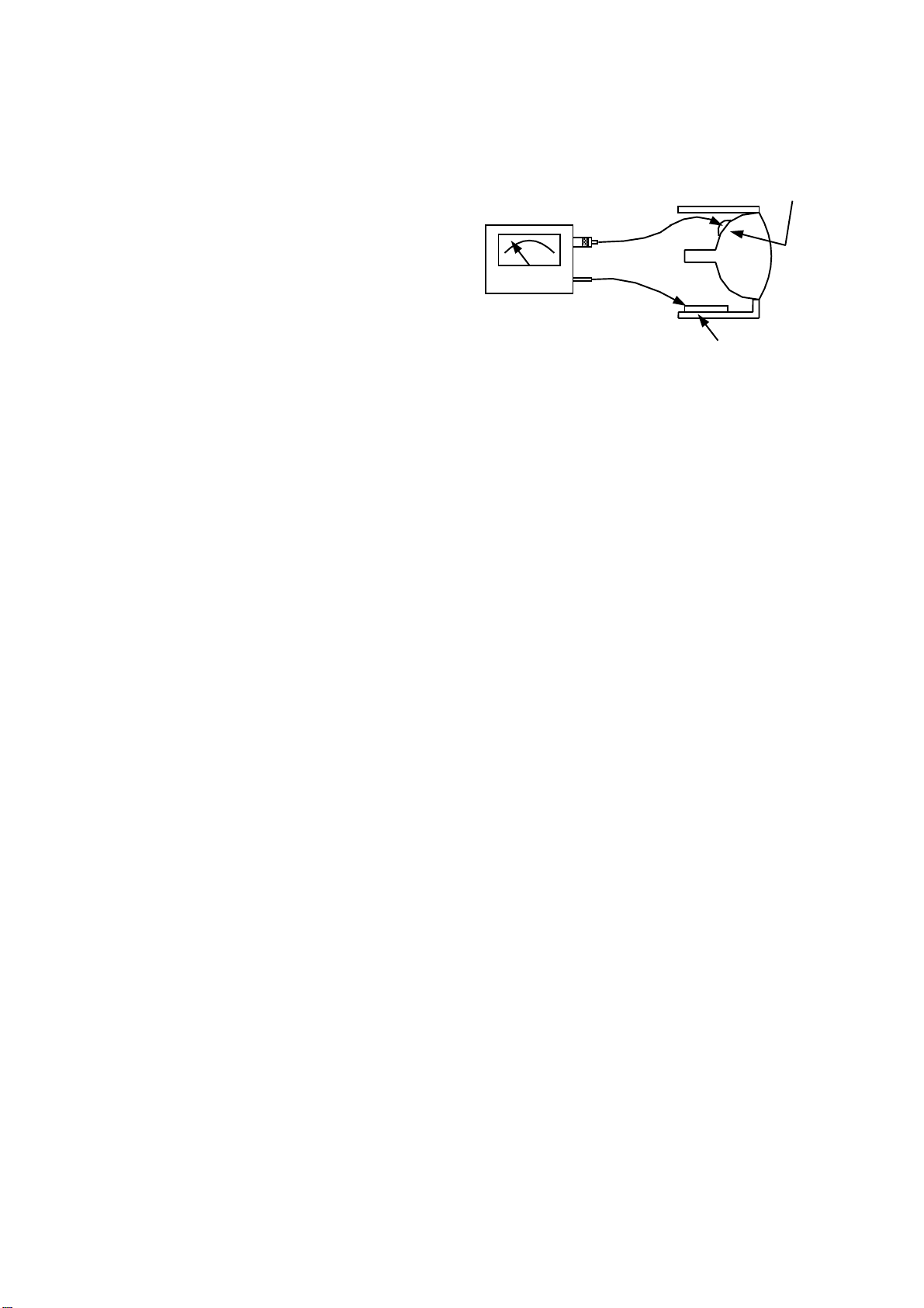
To measure high voltage use a high impedance
high-voltage meter. (SENSITIVE RESEARCH Model:
ESH or Equivalent)
Connect (-) to chassis earth and (+) to the CDT anode
button. (See the following connection diagram Fig. 1.)
NOTE: Turn power switch off without fail before making
the connection to the Anode button
CDT ANODE
(+)
(-)
HIGH IMPEDANCE
H.V. METER
SENSITIVE RESEARCH
Model: ESH or equivalent. CHASSIS GROUND
FIG. 1
X-radiation
TUBE: The source of X-radiation in this monitor is the
picture tube. The tube utilized in this chassis is specially
constructed to limit X-radiation emissions.
For continued X-radiation protection, the replacement
tube must be the same type as the original, manufacturer
approved type.
When troubleshooting and making test measurements in
a monitor with a problem of excessive high voltage, avoid
being unnecessarily close to the picture tube and the high
voltage components.
Do not operate the chassis longer than is necessary to
locate the cause of excessive voltage.
CHECK OF HIGH VOLTAGE HOLD DOWN
CIRCUIT
Checking of the high Voltage hold down circuit operation.
1. Turn the switch of the unit ON, and set the Brightness
and Contrast controls to max.
2. Turn the switch of the unit OFF.
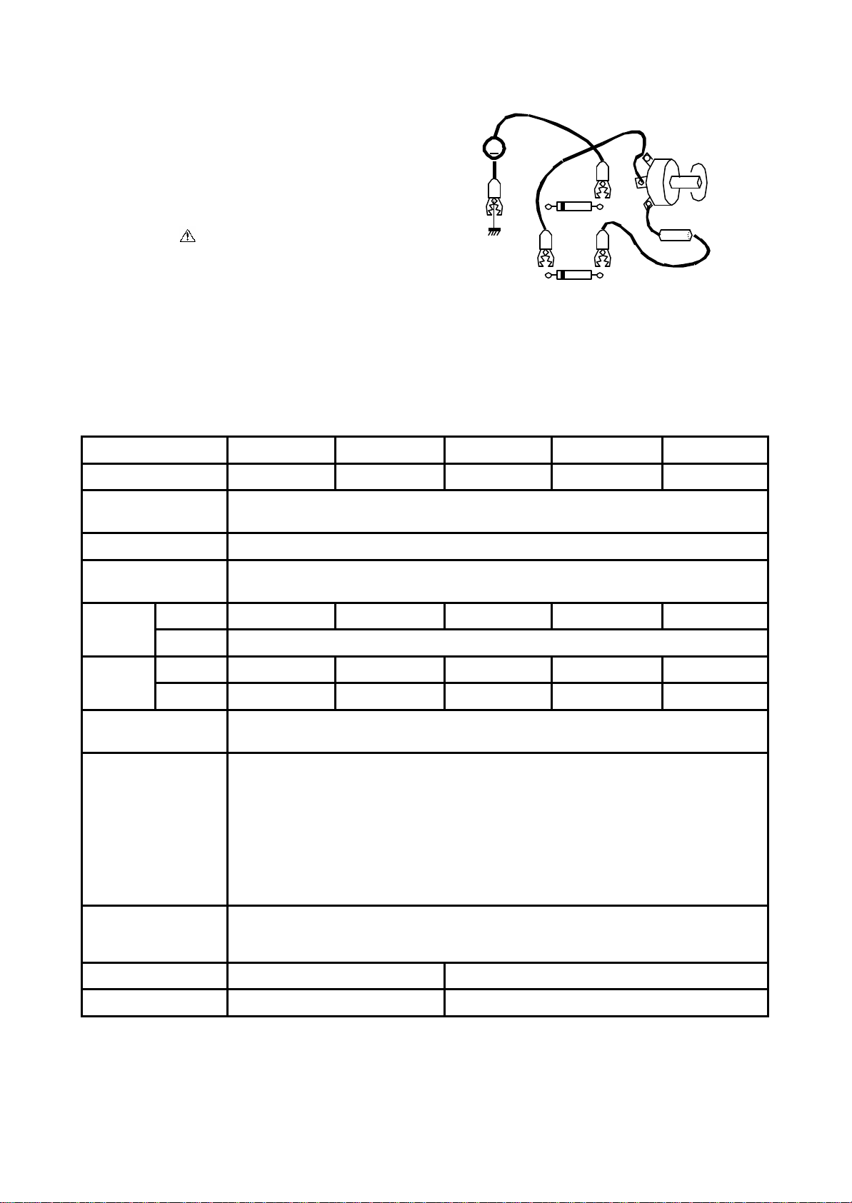
3. Connect a DC Voltmeter and an adjustment jig as
shown in Fig. 2.
4. Set the adjustment VR to fully counterclockwise.
5. Turn the switch of the unit ON and gradually rotate the
adjustment VR clockwise.
6. Check that a reading of DC voltage-meter is less-than
0.6±0.1 V when picture disappears.
7. Turn the switch of the unit OFF immediately after
checking that the picture disappears.
8. Remove the adjusting jig and the DC voltmeter.
NOTE:
Reading of 0.6 V is approximately equivalent to
30 kV of CDT Anode High Voltage.
2
PRODUCT SAFETY NOTICE
R793
R792
Many electrical mechanical parts in the color monitor
units have special safety related characteristics.
These are often not evident from visual inspection nor
can the protection afforded by them necessarily be
obtained by using replacement components rated for
higher voltage, wattage, etc. Replacement parts which
DC VOLT METER
(10 V range)
VARIABLE
V
Clockwise
RESISTER
300 k -B (1/2 W)
have these special safety characteristics are identified in
this Service Manual.
Electrical components having such features are
identified by marking with on the schematics and on
the parts list in this Service Manual.
The use of a substitute replacement component which
does not have the same safety characteristics as the
RESISTER
To
CHASSIS
GROUND
manufacturer recommended replacement one, sh own in
the parts list in this Service Manual, may create shock,
fire, X -radiation, or other hazards.
FIG. 2 CHECKING CIRCUIT USING JIG
DEF BOARD ASSEMBLY
Productions are issued from time to time. For the latest
information, always consult this Service Manual.
SPECIFICATIONS
Model Name CM821FET CM823FET CM827ET CM828ET
Destination Europe Europe Europe Europe
68 k (1/2W)
Rated Voltage AC 100-120 / 200-240 V, Automatically select.
Provided with Power Circuit.
Power Consumption 145 W max (120W typ.)
Color Display Tube
(CDT)
Rated
Frequency
Resolution
Vertical Up to 1392 lines Up to 1536 lines Up to 1392 lines Up to 1536 lines
Horizontal 31 - 107 kHz 31 - 121 kHz 31 - 107 kHz 31 - 115 kHz
Vertical 50 - 160 Hz
Horizontal Up to 1856 dots Up to 2048 dots Up to 1856 dots Up to 2048 dots
21 inches diagonal, 0.21 mm horizontal dot pitch,
Invar shadow mask, Black matrix, Anti-Reflection coat, Short persistence phosphors.
Signal Inputs Red, Green and Blue analog video
H/V separate, H/V composite or Sync. on Green sync (option).
User Controls Power Switch
Degauss
Language Select
Contrast
Brightness
H. Position
H. Size
V. Position
V. Size
Rotation
Pincushion
Trapezoid
Pin.Balance
Parallelogram
H. Moiré
V. Moiré
Color Select
Red, Green, Blue
DMS Mode
OSD H-Position
OSD V -Position
Dynamic Focus
V.Linearity
V.L. Balance
Hemisphere
Total Reset
Single Recall
Top Corner Pin.
Bottom Corner Pin.
H. Convergence adj.
V. Convergence adj.
Environmental
Condition
Operation Storage
Temperature : 5 to 35 -20 to 60
Humidity : 10 % to 80 % 10 % to 90 %
Dimensions 488(W) × 483 (H) × 475 (D) mm * 488(W) × 483 (H) × 470 (D) mm *
Weight 30.5 kg(Net) 27.0 kg(Net)
* Including Tilt & Swivel base
3
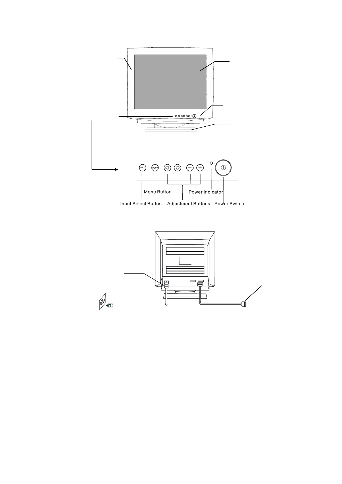
CONTROLS
Front Cover
Control Panel
FIG.3 FRONT VIEW
FIG. 4 CONTROL PANEL
CRT Surface
Tilt & Swivel Base
FIG. 3 FRONT VIEW
Signal Cable
AC Inlet
D-Sub Mini 15-pin
FIG. 5 REAR VIEW
(D-Sub Mini 15-pin)
4
SIGNAL TIMING CHART
CM821F
CM821FET
1 Video Type R/G/B Analog R/G/B Analog R/G/B Analog R/G/B Analog
Voltage 0.7 Vp-p 0.7 Vp-p 0.7 Vp-p 0.7 Vp-p
Set Up None None None None
2 Sync Type H/V Separate H/V Separate H/V Separate H/V Separate
Amp. TTL Level
3 Video frequency 25.175 MHz 56.250 MHz 94.500 MHz 157.500 MHz
4 Character (Letter)
5 Horizontal Frequency 31.469 kHz 53.674 kHz 68.677 kHz 91.146 kHz
Front
Sync.
Back
Blanking
Display
H. period
6 Vertical Frequency 70.086 Hz 85.061 Hz 84.997Hz 85.024 Hz
Front
Sync.
Back
Blanking
Display
H. period
7 Scan System (Non-interlaced) (Non-interlaced) (Non-interlaced) (Non-interlaced)
8 Signal name 30B 54A 68A 91A
* VGA is a registered trademark of International Business Machined Corporation.
* VESA is a trademark of a nonprofit organization, Video Electronics Standard Association.
Signal
0.636 µs (16cl) 0.569 µs (32cl) 0.508 µs (48cl) 0.406 µs (64cl)
porch
3.813 µs (96cl) 1.138 µs (64cl) 1.016 µs (96cl) 1.016 µs (160cl)
width
1.907 µs (48cl) 2.702 µs (152cl) 2.201 µs (208cl) 1.422 µs (224cl)
porch
6.356 µs (160cl) 4.409 µs (248cl) 3.725 µs (352cl) 2.844 µs (448cl)
width
25.422 µs (640cl) 14.222 µs (800cl) 10.836 µs (1024cl) 8.127 µs (1280cl)
time
31.778 µs (800cl) 18.631 µs (1048cl) 14.561 µs (1376cl) 10.971 µs (1728cl)
(1H)
0.381 ms (12H) 0.019 ms (1H) 0.015 ms (1H) 0.011 ms (1H)
porch
0.064 ms (2H) 0.056 ms (3H) 0.044 ms (3H) 0.033 ms (3H)
width
1.112 ms (35H) 0.503 ms (27H) 0.524 ms (36H) 0.483 ms (44H)
porch
1.557 ms (49H) 0.578 ms (31H) 0.582 ms (40H) 0.527 ms (48H)
width
12.711 ms (400H) 11.179 ms (600H) 11.183 ms (768H) 11.235 ms (1024H)
time
14.268 ms (449H) 11.756 ms (631H) 11.765 ms (808H) 11.761 ms (1072H)
(1H)
VGA
640×400
(70Hz)
9999 9999 9999 9999
9999 9999 9999 9999
9999 9999 9999 9999
9999 9999 9999 9999
(Neg./Pos.)
640 dots×400 lines 800 dots×600 lines 1024 dots×768 lines 1280 dots×1024 lines
VESA
800×600
(85Hz)
TTL Level
(Pos./Pos.)
VESA
1024×768
(85Hz)
TTL Level
(Pos./Pos.)
VESA
1280×1024
(85Hz)
TTL Level
(Pos./Pos.)
5
Signal
CM821F
CM821FET
-
-
1 Video Type R/G/B Analog R/G/B Analog R/G/B Analog R/G/B Analog
Voltage 0.7 Vp-p 0.7 Vp-p 0.7 Vp-p 0.7 Vp-p
Set Up None None None None
2 Type H/V Separate H/V Separate H/V Separate H/V Composite
Amp. TTL Level
3 Video frequency 243.500 MHz 288.500 MHz 25.175 MHz 24.800MHz
4 Character (Letter)
5 Horizontal Frequency 112.5 kHz 112.5 kHz 31.469 kHz 31.000 kHz
Front
porch
Sync.
width
Back
porch
Blanking
width
Display
time
H. period
(1H)
6 Vertical Frequency 90.000 Hz 75.000 HZ 59.940 Hz 50.000 Hz
Front
porch
Sync.
width
Back
porch
Blanking
width
Display
time
H. period
(1H)
7 Scan System (Non-interlaced) (Non-interlaced) (Non-interlaced) (Non-interlaced)
8 Signal name 112C 112F 30C 31W
0.263 µs (64cl) 0.444 µs (128cl) 0.636 µs (16cl) 0.403 µs (10cl)
0.790 µs (192cl) 0.778 µs (224cl) 3.813 µs (96cl) 3.790 µs (94cl)
1.251 µs (304cl) 1.222 µs (352cl) 1.907 µs (48cl) 2.258 µs (56cl)
2.305 µs (560cl) 2.444 µs (704cl) 6.356 µs (160cl) 6.452 µs (160cl)
6.584 µs (1600cl) 6.444 µs (1856cl) 25.422 µs (640cl) 25.806 µs (640cl)
8.889 µs (2160cl) 8.889 µs (2560cl) 31.778 µs (800cl) 32.258 µs (800cl)
0.009 ms (1H) 0.009 ms (1H) 0.381 ms (10H) 3.548 ms (110H)
0.027 ms (3H) 0.027 ms (3H) 0.064 ms (2H) 0.129 ms (4H)
0.409 ms (46H) 0.924 ms (104H) 1.049 ms (33H) 3.097 ms (96H)
0.444 ms (50H) 0.960 ms (108H) 1.430 ms (45H) 6.774 ms (210H)
10.667 ms (1200H) 12.373 ms (1392H) 15.253 ms (480H) 13.226 ms (410H)
11.111 ms (1250H) 13.333 ms (1500H) 16.683 ms (525H) 20.000 ms (620H)
VESA
1600×1200
(90Hz)
9 9
9 9
(Pos./Pos.)
1600 dots×1200
lines
VESA
1600×1200
(75Hz)
TTL Level
(Pos./Pos.)
1600 dots×1200
lines
VGA
640×480
(60Hz)
TTL Level
(Neg./Neg.)
640 dots×480 lines 640 dots×410 lines
TTL Level (Neg./Neg.)
Adjustment
signal
6

DESCRIPTION OF CIRCUIT
1. Power Supply Circuit
This model incorporates a wide range universal power supply utilizing a switching regulator (see block diagram in Fig.6).
1.1 AC input
AC input consists of AC inlet, EMI filter (C901~C905,C907) and rectifier (D901~D904). Rectifier circuits adapt to
full-wave method. Inrush current limiting circuit (R90A) protects from excessive inrush current at initial stage of power
on.
1.2 Switching Regulator circuit
Switching Regulator ci rcuit is designed to handle variations of two conditions t o ensure constant +B voltage to secondary circuit :
(Circuit #2) varying load conditions of video, (Circuit #3) varying horizontal frequencies and load conditions.
1.2.1 Circuit #1 :
Circuit #1 consists of chopper inductor (L910), chopper component (Q910), rectifier component (D910, C920) and
control IC (I920). R918 and R919, R91A detect output voltage and provide signal to I920 pin 20 which adjusts the pulse
width based on the pin 20 voltage level to provide constant voltage output.
1.2.2 Circuit #2 :
Circuit #2 consists of chopper transform er (T921), chopper component (Q920) and control IC (I920). T921 detects out put voltage and
provides signal to I920 pin 4 which adjus ts the pulse width based on the pin 4 voltage l evel to provide c onstant voltage output. If the
secondary circuit becomes overloaded, prim ary current through T921 is det ected at R923, R924 and stops the switching operation.
Once the circuit has overloaded, the power switch must be turned off for a short period and then turned on to re-establish power.
Switching frequency is determined by time constant of R92E and R92F, R92G.
1.2.3 Circuit #3 :
Circuit #3 has two outputs. +5V is used mainly to drive the microprocessor circuit and input the signal selection circuit.
+6.3V is used for the CRT heater.
When the DC voltage from circ uit #1 is applied to I 940, I940 s tarts osc illations . Once os cillati ons start, the switching trans is tor is dri ven
by the voltage taken from the terti ary winding of T940. The output vol tage of the T940’s tertiary winding is recti f i ed by D942 and C942.
The main power supply (Circuit #2) turns on (off) when a signal Hi gh (Low) is applied to the base of Q984 from the m icroprocessor
circuit.
1.3 Degaussing circuit
When the power is switched on, the CRT is degaussed automatically by current flowing through the degauss circuit
while the relay (S99R) is closed. Degaussing current flows for approximately 20 seconds and stops by causing relay
(S99R) to be opened after secondary circuit operation is stabilised.
The circuit also allows for manual degauss by using “DEGAUSS” control on OSD menu which closes S99R through
Q991 to allow current to flow through the degauss coil.
7
A
FIG. 6 BLOCK DIAGRAM FOR POWER SUPPLY CIRCUIT
Main power supply
Circuit #2
C inlet
Degauss
Circuit
Manual
Degauss
On/Off
control
5V
Reg.
+B
+85V
+54V
+14V
+ 6.2V
MPU
Heater
Chopper
Chopper
Control
Circuit #1
Circuit #3
+ 12V
Control
Chopper
On/Off
On/Off
control
Standby power supply
8
2. Video Processing Circuit
2.1 Video select circuit (Optional)
Two of Video input signals shall be switched at Video selector (I205) controlled by switching signal coming from
microprocessor.
2.2 Video Processor
The video input signal of 0.7 Vp-p is amplified to approximately 50 Vp-p by the video processing circuit and is fed to the
cathode to drive the beam current.
This chassis incorporates a single chip video processor I201, with three channels, one for each of R/G/B, which
functions as the pre-amp of the inputs, OSD mixer and also gain control. A control signal from the microprocessor
changes the amplifier gain of the video channels (R/G/B) together with white balance control.
Video Output circuit I202 amplifies R/G/B signals controlled by I201 to the enough level to drive Cathode of CRT. DC
voltage of Cathode is determined by DC Cut off voltage from Cathode Clamp Circuit. DC Cut off voltage is generated at
Level Shift Circuit which consists of I203, Q22R, Q22G and Q22B, whose R/G/B channels are also controlled by
microprocessor.
2.3 ACL Circuit
The current at the secondary winding of the flyback transformer is used to represent the CRT beam current. The current
is measured and fed to the contrast control Q281,Q282 to limit the maximum beam current with negative feedback.
2.4 Blanking Circuit
Video blanking during the beam retrace period is achieved by applying both horizontal and vertical blanking pulses to
I201.
2.5 Precedence of Clamp Pulse Circuit
Video Processor I201 receives Clamp pulse signal from I701, Precedence of Clamp Pulse Circuit.
2.6 OSD Circuit
I301 receives H/V pulses from Deflection Circuit and control signal from microprocessor, whose output feeds Clock
signals synchronized with H pulse and control signals from microprocessor, OSD display signals in R/G/B, OSD
blanking signal to OSD Mixer Circuit in I201.
FIG. 7 VIDEO PROCESS CIRCUIT
9
(
)
A
A
)
3. Horizontal Deflection and High Voltage Regulation Circuit
3.1 Horizontal Deflection Circuit
The purpose of the horizontal deflection circuit is to cause the CRT electron beam to be scanned horizontally by driving
a current through the deflection yoke, synchronized by the H sync pulse. The circuit consists of an AFC circuit, made up
of an H phase locked loop and VCO (voltage controlled oscillator), and the deflection output.
The H.sync. signal is input to I701 where it is delayed and then input to a phase detector. The phase locked loop (I701)
also accepts input from a saw tooth waveform which is provided by the deflection feedback (flyback pulse) through the
R707. The output of the phase detector creates an error voltage between the feedback pulse and the input pulse and is
then fed to the VCO after processing by an AFC Filter.
If the oscillator frequency deviates more than 4% of H.SYNC, PLL1 (I701) goes into search mode and HUNLOCK (I701)
changes to “H”. The minimum horizontal frequency is determined by the capacitor at C706 and R704. Horizontal
frequency range is determined by R705. H.SIZE, S.PIN and Trapezium are controlled by PWM circuit (Q801). The
output pulse from the VCO is fed to the pre-drive and then output from I701 to the drive buffer Q701 / Q702. The
pre-drive circuit within I701 is controlled by duty cycle by the internal circuit.
In case of no sync signals supplied or excessive frequency change, such as a s ignal timing change, HUNLOCK once
changes to “H”, and PWM circuit (Q801) output is stopped.
The deflection circuit of the DJ72 chassis has been separated from the high voltage regulation circuit to provide
improved H linearity performance by utilizing the consonant conditions of the horizontal beam current characteristics.
The S-consonant capacitors, C770~C777, are changed by Q767~Q771 and S77R, which provide 8~12 stages of
consonant conditions. The horizontal linearity coils L771~L772 are changed by S77R to provide two stages of H
Linearity conditions.
The H.DEF +B voltage chopper power supply parabolically modulates the H.DEF +B voltage of the deflection circuit,
based on the horizontal frequency, to provide a frequency - dependent voltage of between 42.5V and 160V to the
deflection circuit.
FIG. 8 HORIZONTAL DEFLECTION CIRCUIT
HFLB
V.SYNC
H.CP
V.BLK
From MPU
H.SYNC/Composite SYNC
SEPA
RATER
SDA
SCL
MPU
+B (+200V
I701
14
16
19
18
15
17
5 3 4 6
OSCILLATOR
Drive
Buffer
E / W
H.SIZE
PWM
From
MPU
32
12
13
I601
Vertical
Output
f
H-V
Def
Out
H.DF
mp
mp
H.DRIVER
+B E
V.DY
Lin.
Coil
85V
EHV PWM
Module
Lin.
Coil
T751
T751
L771
S77R
C771~
C777
Q767~
Q771
10
S.fig.
Cap.
From MPU
S.fig.
Cap.
C770
Select Select
From MPU
A
r
FIG. 9 DEFLECTION CONTROL IC BLOCK DIAGRAM
7V
V-sync
clamping
blanking
HUNLOCK
SDA
SCL
I701
14
16
17
19
18
V-Sync
Integrator
Video
Clamping
nd
V-BLANK
HUNLOCK
Output
I2C-BUS
Receiver
H/C-Sync
Vertical
Oscillator
and AGC
V-Position
V-Size,VOVSCN
Protection
and Soft Start
I2C-BUS Registers
Coincidence
Detector
EWDRV
11
EW-Output
H-Pincushion
H-Corner
H-Trapezium
-
1.2V
V-Output
V-Linearity
V-Linearity Balance
FOCUS
Horizontal
and Vertical
H-Size
Control
H-Output
Stage
12
13
32
6
4
3
5
V
OUT2
V
OUT1
Focus
H-Size
Control
Oscillato
HDRV
8
H/C-sync
15
Input and
Polarity
Correction
PLL1 and
H-Position
Horizontal
Oscillator
PLL2,Parallelogram,
Pin Unbalance and
Soft Start
1
HFLB
11
FBT
3.2 High Voltage Regulation Circuit
The output pulse from Q701 is also fed to the high voltage regulation circuit with the same design of consonant circuit as
the horizontal deflection circuit. High voltage of 27.5 kV is obtained by the step-up windings of the flyback transformer to
drive the CRT anode. The high voltage is monitored by the E
error detection circuit. The error detection circuit
HV
functions by stepping the high voltage down and comparing it with the reference voltage of inside I740 whose output
controls I740, the Integrated Circuit included with E
switching transistor.
HV
3.3 Dynamic focus drive circuit
This monitor’s CRT includes a dynamic focusing electron gun to achieve sharp and uniform focus throughout the display
area. The CRT’s Focus anode receives a DC component of approximately 27% of the CRT anode voltage, combined
with the AC voltage parabolic wave form of magnitude of 600 Vp-p horizontal, and 180 Vp-p vertical. DC focus voltage is
obtained from a tap of the flyback transformer’s bleeder resister, and fed to G3 focus electrode. Horizontal and vertical
parabolic output pulses are amplified at Q501~Q508, T506 and fed to the flyback transformer where they are combined
with the DC component (27% of anode voltage). The potentiometers (focus 1, focus 2) at the flyback adjust the DC
focus voltage. The focus 2 potentiometer mainly adjusts horizontal beam shape (vertical line width), and the focus 2
potentiometer mainly adjusts the vertical beam shape (horizontal line width) by optimizing the DC component of the
parabolic waveform.
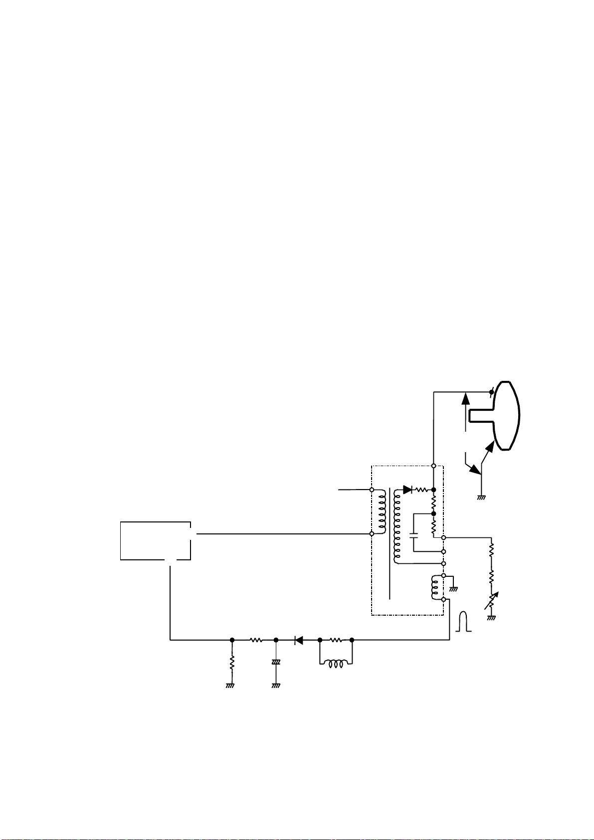
3.4 High Voltage Hold-Down Circuit
DJ82- Chassis uses a system that stops H/V DRIVE SIGNAL output when abnormal high voltage is detected. So that
the high voltage output will be declined to zero. The circuit operation in detail is as follows.
When an input voltage to I740 (pin15, it is determined by R792 and R793) exceeds the specified level, the high voltage
is declined to zero.
FIG.10 HIGH VOLTAGE HOLD-DOWN CIRCUIT DIAGRAM
For the models CM823FU, CM823FET
8
10
E
HV
I740
module
EHV +B
HIGH
VOLTAGE
CRT
R746
R756
R747
R792 R791
R793
+
C791
D790
L791
-
12
4. Vertical Deflection Circuit
The purpose of the vertical deflection circuit is to cause the CRT electron beam to be scanned vertically by driving a
current through the deflection yoke, synchronised by the V sync pulse. V sync is input to the V oscillator circuit, I701,
generating the vertical saw tooth wave. The vertical saw tooth wave is fed to I601 to be amplified of I601 to drive the
vertical deflection yoke.
The feedback circuit inside I601 works such that the differential voltage between pin9 and pin4 equals zero. The
differential input current is compared with the feedback current, and the differential drives the output amplifiers. By
varying resistor R612 or R619 one can set the desired deflection current.
The picture can be shifted in vertical direction by making a DC-offset current through the coil. DC-offset current through
the coil is controlled by the differential input current from I701.
I601 uses an external flyback supply voltage, which is connected to pin7. The signal from the I601 8pin output is used
for protection. The guard output is also activated during thermal shutdown i.e. when Tj>=160
of range.
FIG. 11 VERTICAL DEFLECTION CIRCUIT
V.BLK
I601
83 5 7
P
C609
+
GND
+
C613
V
V
FB
o
C, and feedback loop out
V.SYNC
From MPU
SDA
SCL
I701
V.OUT
14
V.Lin
V.Lin balance
V.Position
19
18
13
12
IN A
IN B
1
2
INPUT
STAGE
GUARD
CIRCUIT
PROTEC
TION
FLYBACK
GENERATOR
AMPLIFIER
A
AMPLIFIER
B
6
OUT A
9
FEEDB
4
OUT B
C610
R620
R619
R611
V.DY
R612
13

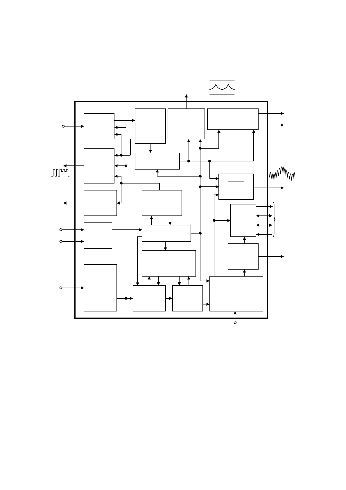
5. Microprocessor Circuit
The microprocessor circuit consists of the following four detailed circuits as shown in Fig.12.
1. Sync detect circuit
2. Front panel key data Input / Output (I/O)
3. Processing and memory
4. Control output
5.1 Sync detect circuit
The sync priority selector (I302) outputs H/V separate or composite sync signal to the sync processor inside the
microprocessor (I101). The sync processor has H/V polarity detector and sync separator for composite sync, H/V
frequency counter, dummy frequency generator, and outputs the processed H/V sync signal to the deflection processing
IC (I701) through the sync selector (I104).
5.2 Front panel key data Input / Output (I/O)
Microprocessor (I101) received user input from the front panel keys, which consists of: one menu key, four adjustment
keys (two pairs)
Contrast and Brightness are adjusted by four adjustment keys when OSD is disappeared.
Other feature requires controlling four adjustment keys when OSD is appeared by a menu key.
Current settings (including picture size, geometry, and color setting) are automatically stored to non-volatile memory.
The maximum memory capacity is for 48 presets including factory standard settings.
5.3 Processing and memory
I101 is an 8-bit microprocessor that equips with ROM and RAM for system program and sync processing circuit. Data
memory consists of one EEPROM chip (I102) for preset data.
5.4 Control output
Output of the microprocessor (I101) controls the deflection processing IC (I701) and the video pre-amplifier IC (I201),
the OSD control IC (I301), the rotation circuit, Horizontal drive correction circuit, the mute circuit, the sync priority
selector (I302), sync selector (I104), power save function. The deflection processing IC receives the signal through I
2
C
Bus to control the geometric function (H/V size and position, Pincushion, Trapezoid, Pin.Balance, Parallelogram, H/V
Moiré, H/V Convergence, Dynamic focus, Top/Bottom corner pincushion, V.Linearity, V.L.Balance). The video
pre-amplifier IC receives the signal through I
receives the signal through I
2
C Bus to control R/G/B Cut off and Contrast, Brightness, Sub BKG, ACL, C-Contrast, and
2
C Bus to control R/G/B Gain and Sub Contrast. The OSD control IC
shows guidance for monitor control function on screen display by generating video signal for OSD and feeding it to video
pre-amplifier IC. Power save function has Standby mode (main power supply has no output if either H sync or V sync is
not supplied) and Off mode (all power supply except +5V have no output if both H sync and V sync are not supplied).
The mute circuit brings video output to black level when timing signal changes or the monitor goes into the power saving
mode.
This chassis is capable of communication with external PC for factory adj ustment through video connector (D-sub).
14
FIG. 12 MICROPROCESSOR CIRCUIT
15
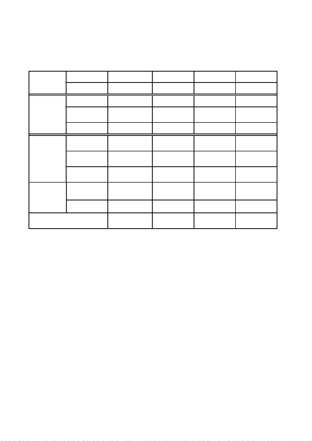
6. Power Save Function
The DJ82 chassis is capable of power savings by sensing of the sync input conditions by the microprocessor. The
microprocessor can identify two sync conditions, (1) No detection of H.sync, (2) No detection of V sync.
The following table shows the details of the Power save mode.
TABLE: POWER SAVE FUNCTION
Sync
V Sync Yes Yes No No
VESA
Standard
Effect None Minimum Minimum Maximum
Circuit
Operation
Video
Power LED CM823F
Power consumption
(Typical) : AC (120V)
H Sync Yes No Yes No
Name Normal Standby Suspend Off
Recovery Time N/A Short Short
H. Deflection
V. Deflection
CM823FET
Normal
operation
Normal
operation
Normal
operation
Lighting
Green
All White : 120 W
All Black : 100 W
System
Dependent
Stop Stop Stop
Stop Stop Stop
Mute Mute Mute
Lighting
Orenge
less than 10W less than 10W less than 3W
Lighting
Orenge
Lighting
Orenge
16
 Loading...