

Page 1
SERVICE MANUAL
8M79B CHASSIS
Description:
MODEL.
Engineering Dept:
Artwork By:
Checked By:
Approved By:
Brand Name:
JOB NO.
Date:
Date:
Date:
SERVICE MANUAL 8M79B
2012-02-04
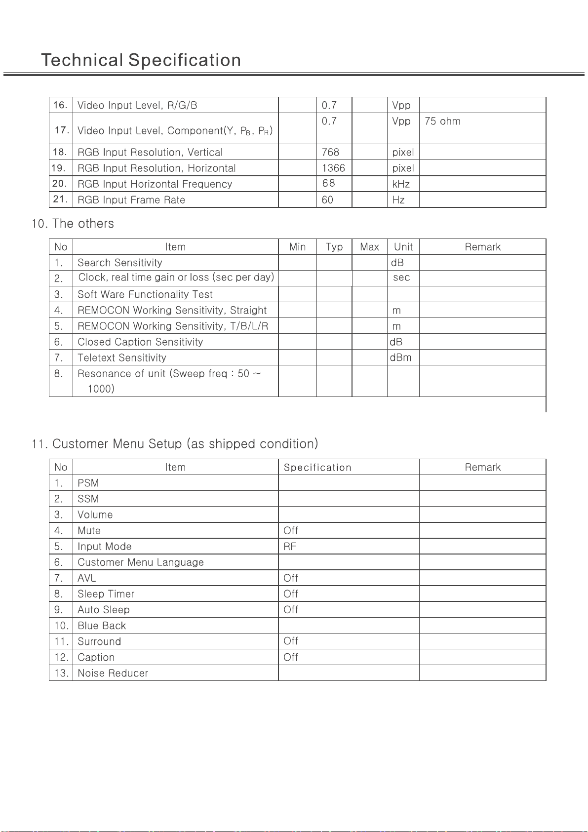
SKYWORTH
SIZE:A5
Design and specifications are subject to change without prior notice.
(Only Referrence)
Page 2

Content-------------------------------------------------------------------------------2
Technical Specification-----------------------------------------------------------3-13
8M79 Block Diagram -------------------------------------------------------------14
List of key parts---------------------------------------------------------------------15
IC BLOCK Diagram----------------------------------------------------------------16-29
MAIN PCB-TOP--------------------------------------------------------------------30
MAIN PCB-BOT--------------------------------------------------------------------31
Circuit Diagrams--------------------------------------------------------------------32-40
-2-
Page 3

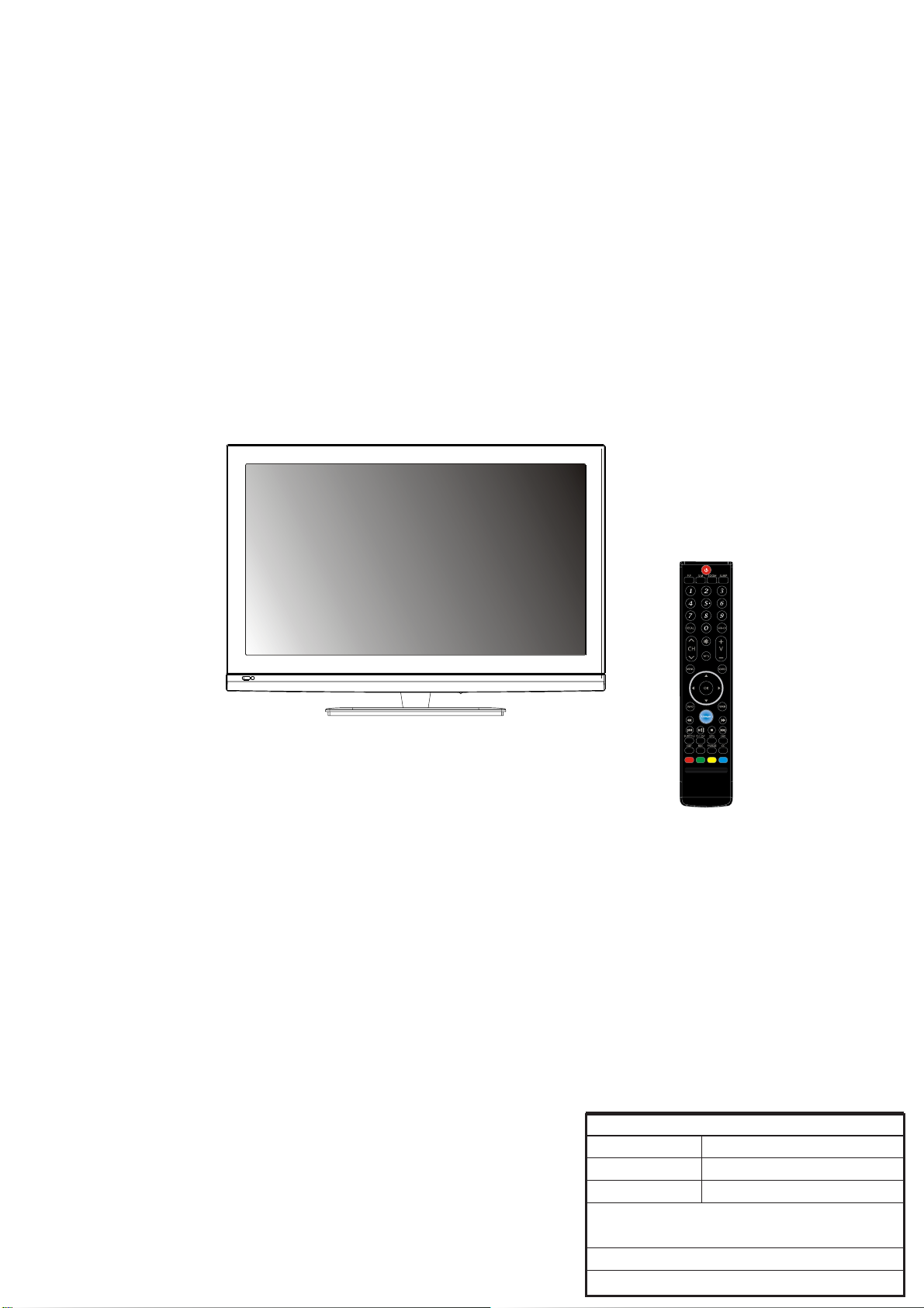
LCD 8M79B chassis.
-3-
Page 4
4.
65
120
For 32LED
For 42LED
Base on different order
5.
-4-
93
93
95
95
400
450
97
97
FOR 32LED
FOR 42LED
Page 5
For 42LED
For 42LED
9800
8
8
12500
12500(266, 276)
9800(280, 290)
6500(313, 329)
-5-
10 15
Page 6
24
40
40
3
1
4.2
50
2
80
0.5
12000
40
6
-6-
Page 7
1080
1920
For 42LED
For 42LED
40
NO
YES
8
6
46
46
NO
Standard
Standard
20
uv
uv
English
No
Middle
-7-
Base on different order
"Low" in some status
Page 8
4
-8-
Page 9
DTV-PRODUCTOINS SPECIFICATION
Model #
Country( West Eu./East Eu./Russia/AP/US/S.A./Japan/…) Brazil & Argentina
Brand Skyworth/ODM
Category (Monitor/TV/Combo/Portable TV…) TV
Panel technology (LCD / PDP) LED
Market Position (High/Mid/Access,,,) Class
Cabinet Design (Example: 01,23 series ) E72
Product Nb Chassis solution MSD309 + ISDB-T Demod
Chassis name 8M79B
Chassis PCB Standard Skyworth RGB New Standard
Predecessor (replace) MP date requested (ETD) 2011.8
MP date confirmed by supplier (ETD/ETA) Status( Pre./Finish ) -
Regional requirement
Homologation (Gostandard/CE/MPTT/CB/…) CB
42"~55"
RoHS Yes
Power supply(100-240V AC +/-10%/...) 100-240V AC (-20%,+10%)
Power consumption working / Annual Power consumption standby <1W
Power plug(VDE/UL/BS/…) UCIEE/2pins
Picture display
Screen size : diagonale (inch) 42", 47",55"
Aspect ratio (16/9 // 4/3 // 15/9) 16:9
1st panel supplier : panel suppliers LG
1st panel supplier : panel reference
Panel Display Type(MVA/PVA/IPS/…) TFT LCD
1st panel supplier : resolution 42/47/55:1920x1080
Dynamic contrast ratio
Video signal process
Comb Filter (2D/3D) 3D
Noise Reduction (adaptative/3D/…) 3D
Picture improvement ( LTI/CTI,BLE,WLE,...) LTI/CTI
Color process (Gama correction/Skin correction /... ) Follow main IC
Colour preset (Cool/Normal/Warm/Personal) Neutral, Cool, Warm and Personal in PC mode
>10000:1
Picture control ( Bright/Con./Sharpness/Color/Tint/…) Yes
Picture presets : Standard / Bright / Soft / User Normal / Soft / Personal / Bright
-9-
Page 10
Picture freeze Yes
Multi picture : PIP ( AV )/POP(AV)
Dynamic Backlight Control No
LED Backlight Yes
Deinterlacer (No/linerar/motion adaptive/motion
compensative)
Film mode / reverse 3:2/2:2 pull down Yes / Yes
Full HD support ( 1080P ) Yes
Single scan / Dual scan ( 120HZ ) Single scan
Zoom type : 4/3 format Yes
Zoom type : 14/9 Zoom Yes
Zoom type : 16/9 Zoom 16/9 ZOOM 1
Zoom type : 16/9 Zoom up/down 16/9 ZOOM 2
Zoom type : Cinerama Yes
Zoom type : 16/9 Format Yes
Zoom type : Auto ( by SCART Pin8 and WSS ) Yes
Picture Auto adjustment (PC mode) Yes
3D Panel Type(PR / SG) PR
3D Mode Left/Right, Up/Down, Frame Sequence
3D To 2D (Y/N) Yes
2D To 3D (Y/N) Yes
Left / Right Swap (For PR Panel) Yes
Sound
Sound type ( Mono/AV stereo/Stereo ) stereo
Music Power (Watt)/RMS Power (Watt) 2 x 8W
Tone control ( Bass&Treble / Graphic Equalizer ) Bass&Treble
Special sound effect ( AVL / WIDE / Pseudo /… ) AVL
Suround system ( Dolby / VD / SRS / BBE / … ) Built-in Surround
Sound control ( Volume , Balance , Mute ) Volume, Balance, Mute
Sound presets (User/Speech/News/Standard) Standard / Music / Film / News / Personal
Headphone volume control ( Separated / linked ) Yes(Linked)
Sound quality ( High / Mid / Low ) Mid
Reception and Decoding capability
RF range(ATV) 54MHz~864MHz
RF range(DTV)
Color System (PAL/SECAM/NTSC/PAL M,N ) PAL M,PAL N,NTSC M
Audio Standard ( B/G/H/D/K/K'/I/L/L' ) M,N
Stereo audio system ( Nicam,MTS,A2,….) BTSC,SAP
Video standard NTSC 3.58 / 4.43 (AV)/PAL 60 NTSC 3.58/4.43 , PAL
DTV SD support (DVB-T/S/C , ATSC , QAM , … ) ISDB-T
DTV HD Support MPEG2,MPEG4,H.264
VHF 177-213 MHZ, UHF 473-803 MHZ
3D motion adaptive
No
MHEG5 No
HD capability with YPbPr Yes (720p; 1080i; 1080p@24/50/60Hz; 480i/p; 576i/p)
PC capability (up to maximum format) Up to 1280X1024 60Hz
HDMI capability (AV/PC Format)
Compatible video format if DVD/USB:
DviX/VCD/SVCD/JPEG/AVI/MPEG2/WMV- HD/SD
JPEG/MPEG2/MPEG4/H.264/DivX (depending on license)
Up to 1080P 24/50/60HZ
-10-
Page 11
Compatible audio format if DVD/USB:
)
t
MP3/WMA/AAC/MPEG1/…
Playable Discs (CD/CD-R(RW)/CD-ROM/DVD+R/+RW/R/-RW
Card reader format compatibility No
Macrovision Yes
PVR
Network No
User convenience
OSD Language* English/Spanish/Portuguese/French
OSD Positioning No
OSD Transparency Adjus
OSD Timeout Adjust No
Customer Brand name(LOGO) Yes
IB languages English
ATV Program Numbers (example: 99+3AV input ) 99+7AV
DTV Program Numbers 370
Program edit ( naming , sorting , skip , swap …. ) Skip / Delete
Auto Naming/Auto Sorting No
TV Guide(DTV EPG) EPG(next Seven-day)
Favorite program Yes
Number of buttons on cabinet (Power; Vol+/-; Pr+/-, Menu
)
Main switch button (yes/No) Yes
CCD(Closed Caption)/V-CHIP
Text Standard: (Top, FLOF,,,) No
Teletext Level: 2.5 / 1.5 Pages for teletext Teletext character sets **** DVB-T teletext -
Real clock From DTV
Sleep timer 10-240 Min.
Timer Turn On / Off, Program Switch
Parent Control -Source and Channel lock (Input code for
certain channel)
Parent Control - Child lock (set the lock of the keyboard,
only the RCU can control the TV)
Parent Control - Kid pass (preset the ontime, channel for
each day of the week)
Parent Control - Channel lock (For digital transmission
and DVD program, to filter some programms)
Calendar / Games No
No program auto switch off 15 mins.
Hotel mode (Y/N) T.B.D
DVD player (No/slot/tray) No
Tuner FM (yes/No) No
software download(RS232/CI/USB/OAD) USB
MP3/WMA(depending on license)
No
Yes(FOR USB)
No
Vol+/-; CH+/-, Menu ,Source,Standby(optional)
Yes/No
Yes
No
No
Yes
Factory reset Yes
-11-
Page 12
Screen saver Yes
Blue Back No
LED indicator(Power on/Standby) Blue / Red
Connectors
RF Input (Antenna): Air/ Cable/ 2in1 Air+Cable
Scart : CVBS in&out / RGB / S-VIDEO No
CINCH video in / out(AV1)
CINCH audio in / out (No volumpe control on Audio
out/can be jack 3,5mm)
S-video in No
Component Video Input (YCrCb/YPrPb) No
Component Audio Input (YCrCb/YPrPb) No
VGA in / Audio L/R in / Jack audio in 3.5mm VGA + dia. 3.5mm for audio in
HDMI 2
DVI No
Audio input for DVI No
CINCH subwoofer out / Coaxial out (S/PDIF) No
Headphone output connector (mm) No
CINCH subwoofer out / Coaxial out (S/PDIF)
RS232 ( Y/N , VGA or DB9 port …) No
Card Readers No
-Rear
No
No
S/PDIF out ( Coaxial )
USB slot (No/1.1/2)
DVB-CI (common interface) No
External power converter input No
Connectors
HDMI 1
AV-IN 1
AV-OUT No
Component Video Input (YCrCb/YPrPb) 1
Component Audio Input (YCrCb/YPrPb) 1 (Share with AV audio in)
Headphone output connector (dia.mm)
CINCH subwoofer out / Coaxial out (S/PDIF) No
USB slot (No/1.1/2)
DVB-CI (common interface) No
DLNA No
UI/RC
UI design (font/pixel, 2D/3D graphic engine..)
RC Model
RC system
RC # of keys
Accessories included
Carton (English/French/Spanish) English
-Side
1 (Software update, JPEG, MP3, WMA, RMVB, DivX) Multimedia
depends on license
1(3.5mm)
1 (Software update, JPEG, MP3, WMA, RMVB, DivX) Multimedia
depends on license
SOD Standard
YK76B3 ( Toshiba code)
RGB Standard
-12-
Page 13
IB English
Circuit diagram No
Batteries Yes
Product registration Card
AC Cable Length 1.8m
Audio Cord (Jack 3.5mm) No
VGA Cord No
Wallmount frame Optional
Antenna Cable No
6 in 1( YPbPr & CVBS) cable adapter No
3D Glasses Yes (2 Sets)
General Data
Size (W x H x D, with stand) in mm Size (W x H x D, without stand) in mm Package Size (W x H x D, without stand) in mm Net Weight in kg Gross Weight in Kg -
Design / Mechanical
Wallmount VESA compatible (standard reference) Yes
Adaptor for VESA wallmount compatibility (accessory ref) Yes
Desktop Stand (included/optionnal + ref/No) included
Panel Tilt (Fowards/Backwards/Rotation) No
Swivel function desktop stand (yes/No) + motorized? No
Docking station (yes/No) No
Floor Stand (included/optionnal + ref/No) No
Glass shield (yes/No) No
Finish on Front Finish on side Finish on back Finish on stand number of colors on carton box 2
Brand logo Customer Inlet
Other logo No
External AC/DC Power with DC power cord (yes/No) No
Handle (yes/No) No
Detachable speaker (yes/No) No
Rating Label langages English
Yes(English)
-13-
Page 14
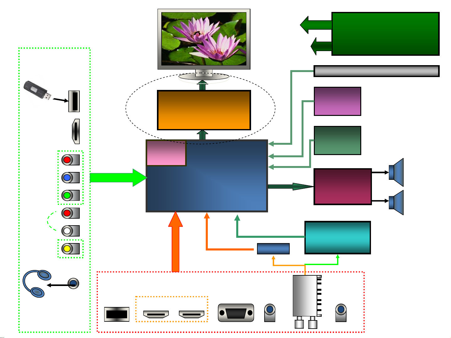
SYSTEM
POWER SUPPLY
Uplayer1
HDMI1
PR
PB
Y
R
L
Video
Optional
PIXELWORKS 3D Processor
Motion Engine
PA131DG
DVB-T&ATV
Demo d
MSD309PX-LF-SB
DVB-T & IF Demo. Build in
MPEG1/2/4 /H.264 Decoder
JPEG MP3 Decoder
3D Comb filter Video Decoder
ATV
DTV
SAW P/S
IF (ATV)
R/L
KEY PAD, IR Receiver ,Ambient Sensor
FLASH
DDRII
TPA3121
10W + 10W
Toshiba TC90517
ISDB-T Demod
IF+/-
Side Terminals
Rear Terminals
Uplayer2
HDMI2
HDMI3
PC PC Audio S/PDIF
Tuner
-14-
Page 15
List of key parts
No. Name Position Type P/N
1 IR U29 HS0038B4 5300-140038-0010
2 Speaker
3 Crystal
4 Tuner U10 VA1P1BF8405 5202-45733D-7H10
5 Saw U30 F4401 4900-744015-0X00
Bass SL-R3018H-3E 5600-106154-0060
Treble YDG3040-2 5600-708254-00
Y2 49U3H 4900-125453-R000
Y1 HC-49U/S 4900-124053-R000
U3 MP1482DS 476A-M14820-0080
U5 MP1482DS 476A-M14820-0080
U50 MP1482DS 476A-M14820-0080
U51 MP1482DS 476A-M14820-0080
U9 W9751G6JB-25 4737-W97511-0840
6
IC
U15 W9751G6JB-25 4737-W97511-0840
U24 EN25F32-100HIP 471R-N25321-0080
U55 TC90517FG 4701-T90510-0640
U37 AS1117L-3.3 47B6-A11170-03
U38 AS1117L-3.3 47B6-A11170-03
N1 AS1117L-3.3 47B6-A11170-03
N2 AS1117L-1.2 47B6-A11175-0300
U54 TPA3121D2PWPR 4722-T31210-0240
U2 MSD309PX-LF-Z1-SB 475C-M30900-5230
-15-
Page 16
IC Block Diagram
Pin Configurations---AS1117L-3.3
L Package
(SOT-223)
3
INPUT
V
OUT
2
OUTPUT
1
ADJ/GND
V
OUT
T Package
U Package
(SOT-89)
3
2
1
R Package
INPUT
OUTPUT
ADJ/GND
)252-OT()022-OT(
3
3
V
OUT
2
1
INPUT
OUTPUT
ADJ/GND
V
OUT
2
1
INPUT
OUTPUT
ADJ/GND
S Package
(TO-263)
3
V
OUT
2
1
INPUT
OUTPUT
ADJ/GND
-16-
Page 17
IC Block Diagram
Pin Configurations---AS1117L-ADJ
L Package
(SOT-223)
3
INPUT
V
OUT
2
OUTPUT
1
ADJ/GND
PIN ASSIGNMENT
The package of AX3113 is SOP-8L; the pin assignment is given by:
Name Description
FB
EN
Ocset
Vcc
1
2
3
4
( Top View )
AX3113
8L
SOP–
FB
Vss
8
Vss
7
6
SW
EN
OCSET
SW
5
V
CC
SW
V
SS
Feedback pin
Power-off pin
HΚnormal operation(Step-down)
LΚStep-down operation stopped
(All circuits deactivated)
Add an external resistor to set max
switch output current.
IC power supply pin
Switch pin. Connect external
inductor & diode here.
GND pin
-17-
Page 18
IC Block Diagram
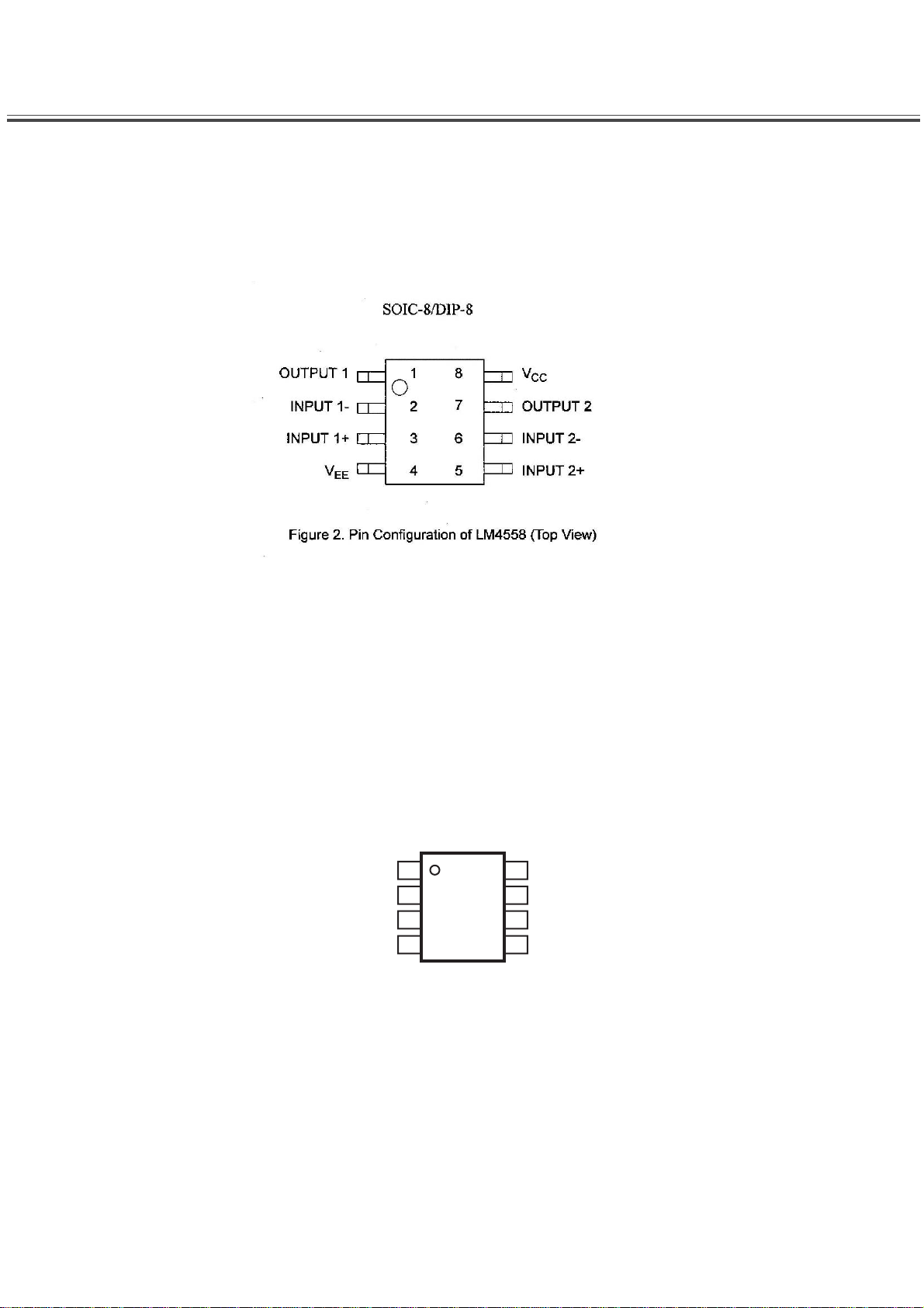
LM4558
MP1482DS
BS
IN
SW
GND
TOP VIEW
1
2
3
4
SS
8
EN
7
COMP
6
FB
5
-18-
Page 19

IC Block Diagram
.
W25X40BVSNIG
PWP (TSSOP) PACKAGE
(TOP VIEW)
PVCCL
SD
PVCCL
MUTE
LIN
RIN
BYPASS
AGND
AGND
PVCCR
VCLAMP
PVCCR
PIN CONFIGURATION
SOIC 150-MIL / 208-MIL
1
2
3
4
5
6
7
8
9
10
11
12
24
23
22
21
20
19
18
17
16
15
14
13
PGNDL
PGNDL
LOUT
BSL
AVCC
AVCC
GAIN0
GAIN1
BSR
ROUT
PGNDR
PGNDR
PAD CONFIGURATION
WSON 6X5-MM
PIN CONFIGURATION
PDIP 300-MIL
-19-
Page 20

IC Block Diagram
Figure.1 CONNECTION DIAGRAMS
8 - LEAD SOP / DIP 8 - CONTACT VDFN
EN25F32
16 - LEAD SOP
-20-
Page 21

IC Block Diagram
Figure 2. BLOCK DIAGRAM
EN25F32
-21-
Page 22

IC Block Diagram
EN25F32
SIGNAL DESCRIPTION
Serial Data Input (DI)
The SPI Serial Data Input (DI) pin provides a means for instructions, addresses and data to be serially
written to (shifted into) the device. Data is latched on the rising edge of the Serial Clock (CLK) input pin.
Serial Data Output (DO)
The SPI Serial Data Output (DO) pin provides a means for data and status to be serially read from
(shifted out of) the device. Data is shifted out on the falling edge of the Serial Clock (CLK) input pin.
Serial Clock (CLK)
The SPI Serial Clock Input (CLK) pi
SPI Mode")
Chip Select (CS#)
The SPI Chip Select (CS#) pin enables and disables device operation. When CS# is high the device is
deselected and the Serial Data Output (DO) pin is at high impedance. When deselected, the devices
power consumption will be at standby levels unless an internal erase, program or status register cycle
is in progress. When CS# is brought low the device will be selected, power consumption will increase to
active levels and instructions can be written to and data read from the device. After
must transition from high to low before a new instruction will be accepted.
Hold (HOLD#)
The HOLD pin allows the device to be paused while it is actively selected. When HOLD is brought low,
while CS# is low, the DO pin will be at high impedance and signals on the DI and CLK pins will be
ignored (don’t care). The hold function can be useful when multiple devices are sharing the same SPI
signals.
n provides the timing for serial input and output operations. ("See
power-up, CS#
Write Protect (WP#)
The Write Protect (WP#) pin can be used to prevent the Status Register from being written. Used in
conjunction with the Status Register’s B
Protect (SRP) bits, a portion or the entire memory array can be hardware protected.
lock Protect (BP0, BP1and BP2) bits and Status Register
Table 1. PIN Names
Symbol Pin Name
CLK Serial Clock Input
DI Serial Data Input
DO Serial Data Output
CS# Chip Enable
WP# Write Protect
HOLD# Hold Input
Vcc Supply Voltage (2.7-3.6V)
Vss Ground
-22-
Page 23

IC Block Diagram
TC90517FG Toshiba products specification [Tentative]
2. Configuration
All functions required for ISDB-T demodulation and error correction are built into the TC90517.
The input signals to be supported are a low IF (intermediate frequency) signal and direct IF signal.
Baseband IQ signals can also be input.
The output signal is an MPEG-2 transport stream (TS) in serial format. Note that a TS in parallel format
can be output by setting registers.
IF input
or IQ input
AGC control output
External AGC input
AGC distortion signal
(reference clock
Tuner I2C• •
Host I2C
Crystal
)
ADC
ADC
SW
I2C
control
Clock PLL
Memory
CONFIDENTIAL
Quadrature
detection
AFC
Tuner
AGC
control
Layer
isolation
Frequency
deinterleaving
Time
deinterleaving
Modulation division
Filter
AGC
Interpolation
• •
correction
Synchroni
Demapping
CSI
processing
Demapping
CSI
processing
Demapping
CSI
processing
phase
zation
ISIC
preecho/postecho
suppression)
Control
demodulation
decoding
Bit deinterleaving• •
(unguarded
TMCC
Viterbi
FFT window
FFT
control
Byte deinterleaving
Fig. 2.1 TC90517FG Block Diagram
(CW interference
Energy
despreading
Energy
despreading
Energy
despreading
Frequency
CPE
CVI
detection)
TS multiplex
Pilot
extraction
CSI
(reliability
detection)
RS
decoding
Adaptive
interpolation
filter
Equalization
Error
detection
Output
control
Synchronization flag
TS output
-23-
Page 24

IC Block Diagram
TC90517FG Toshiba products specification [Tentative]
3. Pin Assignment (Top view)
CONFIDENTIAL
-24-
Page 25

IC Block Diagram
4. Pin Functions
This specification indicates pins and their signals in upper case letters and registers and their signals in lower case
letters.
Pin Pin name
1 TSMD0 I - Shut down 0: Normal operation 1: Shut down
2 XSEL1 I - Crystal frequency division ratio 1 Set according to crystal frequency.
3 XSEL0 I - Crystal frequency division ratio 0 Set according to crystal frequency.
4 VSS - - Digital GND Connects to DGND.
5 SLADRS1 I/O - Slave address 1 Set according to slave address.
6 SLADRS0 I/O - Slave address 0 Set according to slave address.
7 AGCI I - External AGC input Connects to DGND when not used.
8 S_INFO I - Pin for pre-shipment test Connects to DGND.
9 AGCCNTI I/O PD IF_AGC control output Connects to tuner IF_AGC control input pin.
10 AGCCNTR I/O PD RF_AGC control output
11 CKI I - Pin for pre-shipment test Connects to DGND.
12 TNSCL I/O OD I2C clock output
13 VDDS - - I/O power supply Connects to digital +3.3 V typ.
14 TNSDA I/O OD I2C data I/O
15 VSS - - Digital GND Connects to DGND.
16 VDDC - - Digital +1.2 V power supply Connects to digital +1.2 V typ.
17 PLLVSS - - Clock PLL GND Connects to AGND.
18 XO O - Crystal output
19 XI I - Crystal or reference clock input
20 PLLVDD - - Clock PLL power supply Connects to analog +2.5 V typ.
21
22 AD_AVDD - - ADC analog power supply Connects to analog +2.5 V typ.
23 AD_AVSS - - ADC analog GND Connects to AGND.
24 AD_VREFP - - ADC reference voltage output +1.75 V typ. Connects to AGND via PC.
25 AD_VREFN - - ADC reference voltage output +0.75 V typ. Connects to AGND via PC.
26 AD_VREF - - ADC reference voltage output +1.25 V typ. Connects to AGND via PC.
27 ADQ_AIN I -
28 ADQ_AIP I -
29 ADI_AIN I -
FIL O - PLL filter output Connects to AGND via 1500 pF.
(Note4)
30 ADI_AIP I -
I/O
(Note5,7)
PU/PD
Function
Q signal (differential negative side)
input
Q signal (differential positive side)
input
IF signal (differential negative side)
input or I signal (differential
negative side) input
IF signal (differential positive side)
input or I signal (differential
positive side) input
(Note 3)
-25-
(Note 2 and 6)
skrameR
Connects to tuner RF_AGC control input pin.
Open, fixed to L when not used.
Connects to tuner I2C clock pin.
(Pull-up performed outside IC.)
Connects to tuner I2C data pin.
(Pull-up performed outside IC.)
Connects to crystal.
ixosl="1" and open when an external reference clock
is input.
Connects to crystal.
The amplitude (p-p) is 0.5 V to PLLVDD when an
external reference clock is input.
Single-ended IF: Connects to AGND via PC.
Differential IF: Connects to AGND via PC.
Single-ended IQ: Connects to AGND via PC.
Differential IQ: Connects to tuner Q (-) output after
the DC component was cut.
Single-ended IF: Connects to AGND via PC.
Differential IF: Connects to AGND via PC.
Single-ended IQ: Connects to tuner Q output after
the DC component was cut.
Differential IQ: Connects to tuner Q (+) output after
the DC component was cut.
Single-ended IF: Connects to AGND via PC.
Differential IF: Connects to tuner IF (-) output after
the DC component was cut.
Single-ended IQ: Connects to AGND via PC.
Differential IQ: Connects to tuner I (-) output after the
DC component was cut.
Single-ended IF: Connects to tuner IF output after
the DC component was cut.
Differential IF: Connects to tuner IF (+) output after
the DC component was cut.
Single-ended IQ: Connects to tuner I output after the
DC component was cut.
Differential IQ: Connects to tuner I (+) output after the
Page 26

IC Block Diagram
TC90517FG Toshiba products specification [Tentative]
31 AD_DVSS - - ADC digital GND Connects to DGND.
32 AD_ DVDD - - ADC digital power supply Connects to digital +2.5 V typ.
33 VSS - - Digital GND Connects to DGND.
34 DR1VDD - - Digital +1.2 V power supply Connects to digital +1.2 V typ.
35 VDDS - - I/O power supply Con nects to digital +3.3 V typ.
36 VDDC - - Digital +1.2 V power supply Connects to digital +1.2 V typ.
37 VSS - - Digital GND Connects to DGND.
38 STSFLG1 O PD Status flag 1 output Open, fixed to L when not used.
39 DTCLK I PD Pin for pre-shipment test Open or connects to DGND.
40 DTMB I PU Pin for pre-shipment test Open or connects to digital +3.3 V typ.
41 TSMD1 I - Pin for pre-shipment test Connects to DGND.
42 SYRSTN I/O OD System reset input Input at specified timing at power ON.
43 DR2VDD - - Digital +2.5 V power supply Connects to digital +2.5 V typ.
44 VSS - - Digital GND Connects to DGND.
45 SCL I/O OD I2C clock input for host CPU
46 SDA I/O OD I2C data I/O for host CPU
47 VSS - - Digital GND Connects to DGND.
48 DR1VDD - - Digital +1.2 V power supply Connects to digital +1.2 V typ.
49 VDDS - - I/O power supply Con nects to digital +3.3 V typ.
50 VSS - - Digital GND Connects to DGND.
51 STSFLG0 I/O PD Status flag 0 output Open, fixed to L when not used.
52 SLOCK O
53 RERR O - RS decoding error flag output Open, fixed to L when not used.
54 RLOCK O - RS decoding error free flag output Open, fixed to L when not used.
55 RSEORF O - TS error flag output Open, fixed to L when not used.
56 VDDC - - Digital +1.2 V power supply Connects to digital +1.2 V typ.
57 VSS - - Digital GND Connects to DGND.
58 PBVAL O - TS valid flag output Open, fixed to L when not used.
59 SBYTE O - TS synchronization byte flag output Open, fixed to L when not used.
60 SRDT O - Serial TS data output 61 SRCK O - TS serial clock output 62 VSS - - Digital GND Connects to DGND.
63 VDDC - - Digital +1.2 V power supply Connects to digital +1.2 V typ.
64 VDDS - - I/O power supply Con nects to digital +3.3 V typ.
CONFIDENTIAL
Synchronization completion
(sequence 8 or higher) flag
DC component was cut.
Connects to I2C clock bus.
(Pull-up performed outside IC.)
Connects to I2C data bus.
(Pull-up performed outside IC.)
Open, fixed to L when not used.
Note 2 AGND is the abbreviation for analog GND, and DGND is the abbreviation for digital GND.
Note 3 The test dedicated pin is used for the pre-shipment test only. Make sure that processing is performed as
indicated in the "Remarks" column. Any other method will lead to malfunction or failure.
Note 4 I/O indicates the type of the cell used. It may be different from the pin function because a test is conducted
concurrently.
Note 5 PU indicates an I/O with a pull-up resistor (50 k typ.) and PD indicates an I/O with a pull-down resistor (50
k typ.). Pulling down the PU pin or pulling up the PD pin outside the
potential to the midpoint, resulting in instability. Caution is required.
Note 6 The unused output pins must be open and fixed to L by setting the output enable control register of each pin
for noise reduction or set to the output OFF state.
Note 7 OD indicates an open drain I/O. To use the pin for output, pull up the resistance outside the IC.
IC sometimes changes the electric
* The following pins are added with the upgrade from TC90507 to TC90517 (except the changes of power
supply and GND pins):
Pin
Number
21 FIL Added to the PLL loop filter.
27 ADQ_AIN Added for IQ input (differential).
28 ADQ_AIP Added for IQ input.
7 AGCI Added to passthrough the AGC control signal of other ICs.
52 SLOCK Changed from conventional FLOCK.
Pin Name Description
-26-
Page 27

IC Block Diagram
4. B A L L C O N FIG U R A TIO N
1 2 3 4 5 6 7 8 9
PRELIMINARY W9751G6JB
V D D
D Q 14
V D D Q
D Q 12
V D D
D Q 6
V D D Q
D Q 4
V D D L
N C
N C
V S S Q
D Q 9
V S S Q
N C
V S S Q
D Q 1
V S S Q
V S S
U D M
V D D Q
D Q 11
V S S
LD M
V D D Q
D Q 3
V S SV R E F
C K E
W E
B A 0 B A 1
A
B
C
V S S Q
U D Q S
V D D Q
D
E
F
G
H
J
K
L
V S S Q L D Q S
LD Q S
V D D Q
D Q 2
V S S D L
R A S
C A S
U D Q S
V S S Q
D Q 8
V S S QD Q 10
V S S Q
D Q 0
V S S Q
C L K
C L K
C S
V D D Q
D Q 15
V D D Q
D Q 13
V D D Q
D Q 7
V D D Q
D Q 5
V D D
O D T
V S S
A 1 0 /A P
A 3
A 1
A 5
M
N
P
V D D A 1 2 N C N CN C
R
-27-
A 1 1 A 8A 9A 7
A 2
A 6
A 0
A 4
V D D
V S S
Page 28

IC Block Diagram
5. BALL DESCRIPTION
PRELIMINARY W9751G6JB
BALL NUMBER SYMBOL
M8,M3,M7,N2,N8,N3
,N7,P2,P8,P3,M2,P7
,R2
L2,L3 BA0−BA1 Bank Select
G8,G2,H7,H3,H1,H9
,F1,F9,C8,C2,D7,D3,
D1,D9,B1,B9
K9 ODT
F7,E8
B7,A8
L8
K7,L7,K3
B3,F3
J8,K8
K2 CKE Clock Enable
J2 VREF Reference Voltage VREF is reference voltage for inputs.
A1,E1,J9,M9,R1 VDD Power Supply
A3,E3,J3,N1,P9 VSS Ground Ground.
A9,C1,C3,C7,C9,E9,
G1,G3,G7,G9
A7,B2,B8,D2,D8,E7,
F2,F8,H2,H8
A2,E2,L1,R3,R7,R8 NC No Connection No connection.
J7 VSSDL DLL Ground DLL Ground.
J1 VDDL DLL Power Supply
A0−A12 Address
DQ0−DQ15
LDQS,
LDQS
UDQS,
RAS , CAS
UDM
LDM
CLK,
CLK
VDDQ DQ Power Supply
VSSQ DQ Ground DQ Ground. Isolated on the device for improved noise immunity.
FUNCTION DESCRIPTION
Provide the row address for active commands, and the column
address and Auto-precharge bit for Read/Write commands to select
one location out of the memory array in the respective bank.
Row address: A0−A12.
Column address: A0−A9. (A10 is used for Auto-precharge)
BA0−BA1 define to which bank an ACTIVE, READ, WRITE or
PRECHARGE command is being applied.
Data Input
/ Output
On Die Termination
Control
LOW Data Strobe
UP Data Strobe
Chip Select
Command Inputs
Input Data Mask
Differential Clock
Inputs
Bi-directional data bus.
ODT (registered HIGH) enables termination resistance internal to the
DDR2 SDRAM.
Data Strobe for Lower Byte: Output with read data, input with write
data for source synchronous operation. Edge-aligned with read data,
center-aligned with write data. LDQS corresponds to the data on
DQ0−DQ7.
is enabled via the control bit at EMR (1)[A10 EMRS command].
Data Strobe for Upper Byte: Output with read data, input with write
data for source synchronous operation. Edge-aligned with read data,
center-aligned with write data. UDQS corresponds to the data on
DQ8−DQ15.
is enabled via the control bit at EMR (1)[A10 EMRS command].
All commands are masked when
HIGH.
multiple ranks.
RAS , CAS andWE (along with CS) define the command being
entered.
DM is an input mask signal for write data. Input data is masked when
DM is sampled high coincident with that input data during a Write
access. DM is sampled on both edges of DQS. Although DM pins are
input only, the DM loading matches the DQ and DQS loading.
CLK and CLK are differential clock inputs. All address and control
input signals are sampled on the crossing of the positive edge of CLK
and negative edge of CLK . Output (read) data is referenced to the
crossings of CLK and CLK (both directions of crossing).
CKE (registered HIGH) activates and CKE (registered LOW)
deactivates clocking circuitry on the DDR2 SDRAM.
Power Supply: 1.8V ± 0.1V.
DQ Power Supply: 1.8V ± 0.1V.
DLL Power Supply: 1.8V ± 0.1V.
provides for external bank selection on systems with
is only used when differential data strobe mode
LDQS
is only used when differential data strobe mode
is registered
is considered part of the command code.
-28-
Page 29

IC Block Diagram
6. BLOCK DIAGRAM
PRELIMINARY W9751G6JB
CLK
CLK
CKE
RAS
CAS
CS
WE
A10
A11
A12
BA0
BA1
DLL
CLOCK
BUFFER
CONTROL
SIGNAL
COMMAND
DECODER
A0
REFRESH
COUNTER
ADDRESS
BUFFER
A9
GENERATOR
MODE
REGISTER
COLUMN
COUNTER
COLUMN DECODER
CELL ARRAY
BANK #0
SENSE AMPLIFIER
PREFETCH REGISTER
DATA CONTROL
COLUMN DECODER
CIRCUIT
COLUMN DECODER
CELL ARRAY
BANK #1
SENSE AMPLIFIER
DQ
BUFFER
COLUMN DECODER
ODT
CONTROL
ODT
DQ0
|
DQ15
LDQS
LDQS
UDQS
UDQS
LDM
UDM
CELL ARRAY
BANK #2
SENSE AMPLIFIER
NOTE: The cell array configuration is 8192 * 1024 * 16
-29-
CELL ARRAY
BANK #3
SENSE AMPLIFIER
Page 30

MAIN PCB-TOP
-3
0 -
Page 31

MAIN PCB-BOT
-31-
Page 32

5
Power Input
3.3VU
24VA5VU 12VA
R319 1kR319 1k
H:ON
L:OFF
R342 100RR342 100R
C178
C178
0.1u
0.1u
D D
PWR-ON/OFF2
24VA12VA 12-24
L108 FBL108 FB
L116 NC/FBL116 NC/FB
STB
PB-ADJUST
PB-ON/OFF
Note: C103,C104 close to CON6 for EMI
C118
C118
0.1u
0.1u
C1051nC105
14
13
12
11
10
9
8
7
6
5
4
3
2
1
CON25-J25-14
CON25-J25-14
4
1.32V DC-DC
5VA
1482EN
1n
CON6
CON6
CA54
CA54
100uF/16V
100uF/16V
+
+
R52 10kR52 10k
C116
C116
0.1u
0.1u
C141nC14
1n
R29
R29
4.7k
4.7k
1482COMP
7
6
8
0.1u
0.1u
C123
C123
4
For MCU
1.8V DC-DC
5VA
1482EN18
R53 10kR53 10k
+
+
C396
C396
10u
10u
CA12
CA12
100uF/16V
100uF/16V
1482COMP18
C151nC15
1n
R30
R30
4.7k
4.7k
7
6
8
0.1u
0.1u
C128
C128
4
U50
U50
MP1482
MP1482
VCC2OUT
EN
COMP
SS
GND
U51
U51
MP1482
MP1482
VCC2OUT
EN
COMP
SS
GND
3
2
1
DC-DC Module
1.32V
43K_1%
43K_1%
R14
R14
CA2
CA2
470uF/16V
470uF/16V
5VA
C4
C6
10uC410u
+
+
0.1uFC60.1uF
1482OUT
C122
C122
0.1u
0.1u
1482FB
1482OUT18
C127
C127
0.1u
0.1u
1482FB18
L37 22uHL37 22uH
L38 22uHL38 22uH
R57
R57
2.2K
2.2K
R55
R55
4.7K
4.7K
2010-3-14
R60
R60
10K_1%
10K_1%
R58
R58
10K_1%
10K_1%
+
+
470uF/16V
470uF/16V
+
+
470uF/16V
470uF/16V
CA17
CA17
Low ESR
CA18
CA18
Low ESR
1.8VA
C114
C114
0.1u
0.1u
C389
C389
0.1u
0.1u
3
1
BST
5
FB
3
1
BST
5
FB
12VA
L2FBL2
FB
C1
+
+
CA1
CA1
0.1uFC10.1uF
100uF
100uF
U3
MPS1482U3MPS1482
2
IN
R41
R41
100K
100K
C383
C383
3.3nF
3.3nF
R40
R40
5.6K
5.6K
SW
4
GND
BS
6
COMP
7
EN
FB
8
SS
C11
C11
47NF
47NF
L3 22uHL3 22uH
3
C3
10nFC310nF
C386ncC386
1
nc
5
R18 2K_1%R18 2K_1%
R12
R12
10K_1%
10K_1%
C2
1nFC21nF
5V DC-DC
For DDR
C C
MST Power supply
4
ADJ
OUT
ADJ
OUT
IN
U37
U37
AMS1117-3.3V
AMS1117-3.3V
CA40
CA40
100uF/16V
100uF/16V
B B
U38
U38
AMS1117-3.3V
AMS1117-3.3V
5VA
IN
321
3.3VU5VU
C387
NC/0.1u
NC/0.1u
OUT
OUT
C387
C385
C385
+
0.1u
0.1u
CA7 100uF/16V+CA7 100uF/16V
4
IN
IN
321
3.3VA
D38 1N4001D38 1N4001
C384
C384
+
+
CA8
CA8
0.1u
0.1u
100uF/16V
100uF/16V
C378
C378
+
+
0.1u
0.1u
ADJ
ADJ
C379
C379
0.1u
0.1u
3.3VU
380mA 150mA
C377
C377
0.1u
0.1u
2.5VA
230mA
C391
C391
C393
C393
NC/0.1u
NC/0.1u
0.1u
+
+
CA6
CA6
100uF/16V
100uF/16V
0.1u
3.3VA
C380
C380
C394
C394
0.1u
0.1u
NC/0.1u
NC/0.1u
1.32V
C407
C407
NC/0.1u
NC/0.1u
1100mA
C410
C410
NC/0.1u
NC/0.1u
1.8VA
C439
C439
0.1u
0.1u
1.8VA
C432
C432
0.1u
0.1u
1.8VA
110mA
C399
C412
C412
0.1u
0.1u
C399
C400
C400
0.1u
0.1u
0.1u
0.1u
C442
C442
0.1u
0.1u
C450
C450
C473
C473
0.1u
0.1u
0.1u
0.1u
300mA_DDR2 Max
C445
C445
C441
C441
C468
C468
C443
0.1u
0.1u
0.1u
0.1u
C443
0.1u
0.1u
0.1u
0.1u
C401
C401
0.1u
0.1u
C436
C436
C438
C438
0.1u
0.1u
C427
C427
0.1u
0.1u
C452
C452
0.1u
0.1u
0.1u
0.1u
C429
C429
C444
C444
0.1u
0.1u
0.1u
0.1u
PANEL POWER
12VA
PL12V FBPL12V FB
5VA VCC-Panel
PL5V NC/FBPL5V NC/FB
R22
R22
10K
10K
R271KR27
Q409
Q409
ON_PANEL2
H:ON
L:OFF
1
3904
3904
1K
2 3
C104 10nC104 10n
Inverter Interface
3.3VA
R19
R19
10K
10K
L:ON
H:OFF
R24 1KR24 1K
ON_PBACK2
NC
R10NCR10
R203
R203
NC/100K
VCC-PL
+
+
CA11
CA11
100uF/16V
100uF/16V
100R
100R
C3341nC334
1n
1
2
3
PB-ON/OFF
NC/100K
U1
S
S
S
G4D
CEM9435AU1CEM9435A
8
D
7
D
6
D
5
+
+
CA10
CA10
100uF/16V
100uF/16V
VCC-PL
R37
R37
C13
C13
10K
10K
0.1uF
0.1uF
C32
C32
R44
R44
NC/0.1uF
NC/0.1uF
10K
10K
Q411
Q411
1
3904
3904
2 3
5VA
R20
R20
10K
10K
R21
R21
Q407
Q407
1
3904
3904
2 3
USB Power
12VA
L8FBL8
FB
R45
R45
C25
C25
+
+
CA4
CA4
100uF/16V
100uF/16V
A A
ON_USB_MOS8
100K
100K
10uF
10uF
R43
R43
5.6K
5.6K
C37
C37
0.1uF
0.1uF
C475
C475
0.1uF
0.1uF
R178 NC/10KR178 NC/10K
5
C481
C481
3.3nF
3.3nF
U5
MPS1482U5MPS1482
2
IN
SW
4
GND
BS
6
COMP
7
EN
FB
8
SS
5V DC-DC
L9
C495
C495
3
22uHL922uH
10nF
10nF
C31ncC31
1
nc
5
+5V_USB Power trace width
should be > 40mil
C29
C29
1nF
1nF
R42
R42
2K_1%
2K_1%
47K_1%
47K_1%
10K_1%
10K_1%
+5V_USB
R49
R49
+
+
CA19
CA19
470uF/16V
470uF/16V
R46
R46
4
For Power Drop
5VU
12VA
D141
C34
C34
0.1uF
0.1uF
D141
9.1V
9.1V
R339
R339
10K
10K
R74
R74
11K
11K
R67
R67
4.7K
4.7K
C449
C449
10n
10n
1
R68
R68
Q413
Q413
2.2K
2.2K
3904
3904
3
R76
R76
39K
39K
D139
D139
2 3
4.1V
4.1V
DD31
DD31
BAT54
BAT54
HW-RST
2
1
Q415
Q415
2 3
3904
3904
HW-RST 2
R69
R69
10K
10K
1
LEDR 2
DCR-OUT2
ADJ-PWM2
R31 NC/0R31 NC/0
R25 0R25 0
R39 NC/0R39 NC/0
DCR-IN2
R17 4.7KR17 4.7K
Power Test Point
1
TP3TP3
5VU
1
TP4TP4
12VA
1
TP5TP5
3.3VU
1
TP6TP6
3.3VA
1
TP7TP7
2.5VA
1
TP11TP11
VCC-PL
3
2
5V_TUNER
VCC-Panel
1.8VA
1.32V
1
TP22TP22
1
TP12TP12
1
TP8TP8
1
TP9TP9
5VA
R15
R15
10K
10K
PB-ADJUST
R16 0 / 22kR16 0 / 22k
C255
C255
Q406
Q406
NC/0.1u
1
2 3
Title
Title
Title
Size Document Number Rev
Size Document Number Rev
Size Document Number Rev
A2
A2
A2
Date: Sheet of
Date: Sheet of
Date: Sheet
NC/0.1u
3904
3904
Note: Left C255 NC if want to output PWM puls
POWER
POWER
POWER
1/10 0.1
1/10 0.1
1/10 0.1
1
110Saturday, July 02, 2011
110Saturday, July 02, 2011
110Saturday, July 02, 2011
of
Page 33

5
MSD309PX
U2C MSD309PX
U2C MSD309PX
HDMI
HDMI
R53410K R53410K
R50522R R50522R
R50622R R50622R
R50722R R50722R
R50822R R50822R
HW-RST
IR_SYNC
R2121MR212
1M
SPI-CSNI
SPI-SCKI
SPI-SDII
SPI-SDOI
FLASH_WP
G2
H3
H2
J3
J2
J1
G3
G1
M4
M5
K6
D2
E3
E2
F3
F2
F1
D3
D1
J6
L6
J4
AC8
AD9
AC9
AD10
AE10
AC10
AE8
AD8
AE7
AD7
AC7
K5
M2
M3
L2
L3
K1
K3
K2
N4
N5
R3
P2
P3
N2
N3
M1
N1
W6
Y6
U2
U3
T2
T1
R1
R2
T3
V4
AB25
AB24
E6
D6
J5
G4
B4
AA7
C4
A4
A2
B3
A3
B2
P6
N6
AA23
AA24
G5
XTALI
AD1
XTALO
AE2
E5
C2
B1
AD11
AE11
F11
E11
PAD_RX0N_A
PAD_RX0P_A
PAD_RX1N_A
PAD_RX1P_A
PAD_RX2N_A
PAD_RX2P_A
PAD_RXCN_A
PAD_RXCP_A
DDCDA_CK
DDCDA_DA
PAD_HOTPLUGA
PAD_RX0N_B
PAD_RX0P_B
PAD_RX1N_B
PAD_RX1P_B
PAD_RX2N_B
PAD_RX2P_B
PAD_RXCN_B
PAD_RXCP_B
DDCDB_CK
DDCDB_DA
HOTPLUGB
PAD_RX0N_C
PAD_RX0P_C
PAD_RX1N_C
PAD_RX1P_C
PAD_RX2N_C
PAD_RX2P_C
PAD_RXCN_C
PAD_RXCP_C
DDCDC_CK
DDCDC_DA
PAD_HOTPLUGC
PAD_CEC
U2E MSD309PX
U2E MSD309PX
RGB CVBS
RGB CVBS
PADA_RIN0M
PADA_RIN0P
PADA_GIN0M
PADA_GIN0P
PADA_BIN0M
PADA_BIN0P
PADA_SOGIN0
PAD_HSYNC0
PAD_VSYNC0
PADA_RIN1M
PADA_RIN1P
PADA_GIN1M
PADA_GIN1P
PADA_BIN1M
PADA_BIN1P
PADA_SOGIN1
PAD_HSYNC1
PAD_VSYNC1
PADA_RIN2M
PADA_RIN2P
PADA_GIN2M
PADA_GIN2P
PADA_BIN2M
PADA_BIN2P
PADA_SOGIN2
PAD_HSYNC2
U2D MSD309PX
U2D MSD309PX
PAD_PWM0
PAD_PWM1
PAD_PWM2
PAD_PWM3
PAD_SAR0
PAD_SAR1
PAD_SAR2(POWER_DET)
PAD_SAR3
PAD_GPIO_PM6(BOOT_FLASH_CS)
PAD_SPI_CZ(BACKUP_FLASH_CS)
PAD_SPI_CK
PAD_SPI_DI
PAD_SPI_DO
PAD_GPIO_PM8(FLASH_WP)
DDCA_CK
DDCA_DA
PAD_DDCR_CK
PAD_DDCR_DA
PAD_IRIN
PAD_XTAL_IN
PAD_XTAL_OUT
PAD_RESET
PAD_DP_P0
PAD_DM_P0
PAD_DP_P1
PAD_DM_P1
PAD_GND_EFUSE
PAD_TESTPIN
PWM
PWM
SAR
SAR
SPI
SPI
UART/I2CS
UART/I2CS
I2CM
I2CM
IR
IR
XTAL
XTAL
RESET
RESET
USB
USB
PADA_CVBS_OUT1
PADA_CVBS_OUT2
RXA0N6
RXA0P6
RXA1N6
RXA1P6
RXA2N6
RXA2P6
RXACLKN6
RXACLKP6
DDCASCL6
DDCASDA6
HOTPLUGA6
RXB0N6
D D
RXB0P6
RXB1N6
RXB1P6
RXB2N6
RXB2P6
RXBCLKN6
RXBCLKP6
DDCBSCL6
DDCBSDA6
HOTPLUGB6
RXC0N6
RXC0P6
RXC1N6
RXC1P6
RXC2N6
RXC2P6
RXCCLKN6
RXCCLKP6
DDCCSCL6
DDCCSDA6
HOTPLUGC6
HDMI-CEC6 SPDIFO 7
RGB0_RIN-7
RGB0_RIN+7
RGB0_GIN-7
RGB0_GIN+7
RGB0_BIN-7
RGB0_BIN+7
RGB0-SOG7
VGA_HSYNC7
VGA_VSYNC7
RGB1_R-7
RGB1_R+7
RGB1_G-7
RGB1_G+7
RGB1_B-7
RGB1_B+7
RGB1_SOG7
C C
COMP_R-7
COMP_R+7
COMP_Y-7
COMP_Y+7
COMP_B-7
COMP_B+7
COMP_SOG+7
PWM0
PWM1
ADJ-PWM1
KEY0
KEY1
SPI-CSN
SPI-SCK
SPI-SDI
SPI-SDO
UART-RX
UART-TX
SCL
SCL10
B B
SDA
SDA10
C173
C173
39p
39p
Y1
3
24MHZY124MHZ
C172
C172
1 2
R476 0RR476 0R
39p
39p
USB_DP8
USB_DM8
USB1_DP8
USB1_DM8
RESET
A A
3.3VU
3
DD30
DD30
BAV99
BAV99
R253
R253
100K
100K
1
R259 10KR259 10K
C308
C308
2.2u
2.2u
C309 0.1uC309 0.1u
2
1
3906
3906
Q41
Q41
HW-RST
R249 100RR249 100R
3 2
R252
R252
100K
100K
C3071nC307
1n
5
AUDIO
AUDIO
PAD_LINEIN_L0
PAD_LINEIN_R0
PAD_LINEIN_L1
PAD_LINEIN_R1
PAD_LINEIN_L2
PAD_LINEIN_R2
PAD_LINEIN_L5
PAD_LINEIN_R5
PAD_LINEOUT_L0
PAD_LINEOUT_R0
PAD_LINEOUT_L3
PAD_LINEOUT_R3
PAD_EARPHONE_OUTL
PAD_EARPHONE_OUTR
PAD_VRP
PAD_VAG
AVSS_VRM_ADC_DAC
PAD_I2S_OUT_MCK
PAD_I2S_OUT_SD
PAD_I2S_OUT_WS
PAD_I2S_OUT_BCK
PAD_I2S_IN_BCK(USB_OCD)
PAD_I2S_IN_SD(LED_ON)
PAD_I2S_IN_WS(WARM_LED_ON)
SPDIF
SPDIF
PAD_SPDIF_OUT
AC5
PADA_CVBS0
W4
PADA_CVBS1
W5
PADA_CVBS2
AA5
PADA_CVBS3
W2
PADA_CVBS4
W3
PADA_CVBS5
CVBS_OUT
V3
AA4
W1
PADA_VCOM
PADA_OUTP_CH[6](PAD_R_ODD[7])
PADA_OUTN_CH[6](PAD_R_ODD[6])
PADA_OUTP_CH[7](PAD_R_ODD[5])
PADA_OUTN_CH[7](PAD_R_ODD[4])
PADA_OUTP_CH[8](PAD_R_ODD[3])
PADA_OUTN_CH[8](PAD_R_ODD[2])
PADA_OUTP_CH[9](PAD_R_ODD[1])
PADA_OUTN_CH[9](PAD_R_ODD[0])
PADA_OUTP_CH[10](PAD_G_ODD[7])
PADA_OUTN_CH[10](PAD_G_ODD[6])
PADA_OUTP_CH[11](PAD_G_ODD[5])
PADA_OUTN_CH[11](PAD_G_ODD[4])
PADA_OUTP_CH[12](PAD_G_ODD[3])
PADA_OUTN_CH[12](PAD_G_ODD[2])
PADA_OUTP_CH[13](PAD_G_ODD[1])
PADA_OUTN_CH[13](PAD_G_ODD[0])
PADA_OUTP_CH[14](PAD_B_ODD[7])
PADA_OUTN_CH[14](PAD_B_ODD[6])
PADA_OUTP_CH[15](PAD_B_ODD[5])
PADA_OUTN_CH[15](PAD_B_ODD[4])
PADA_OUTP_CH[16](PAD_B_ODD[3])
PADA_OUTN_CH[16](PAD_B_ODD[2])
PADA_OUTP_CH[17](PAD_B_ODD[1])
PADA_OUTN_CH[17](PAD_B_ODD[0])
PAD_TCON2(FE_ANT5V_MONITOR)
PAD_TCON3(TUNER_RESET)
PAD_TCON5(SC1_MUTE)
PAD_TCON6(PCM_5V_CTL)
PAD_TCON7(SIDE_AV_DET)
PAD_TCON9(COMP_DET)
PAD_TCON11(HP_MUTE)
PAD_TCON15(SC1_DET)
PAD_GPIO0(NTP_MUTE)
PAD_GPIO3(PANEL_CTL)
PAD_GPIO5(ERROR_OUT)
PAD_GPIO12(AMD_SCL)
PAD_GPIO13(AMP_SDA)
PAD_GPIO_PM0(5V_HDMI_3)
PAD_GPIO_PM1(5V_HDMI_1)
PAD_GPIO_PM4(POWER_ON_OFF)
PAD_GPIO_PM5(5V_HDMI_2)
PAD_GPIO_PM11(DSUB_DET)
PAD_GPIO_PM12(EDID_WP)
LED
3.3VU
R411 2.2KR411 2.2K
R4
R5
T6
U6
V6
U5
AD6
AC6
V1
V2
AA6
Y5
AD5
AE5
AB4
AB5
AC3
I2S
I2S
A6
B5
B6
C6
C1
H6
G6
P5
AV1-Vin+
AV4-Vin+ 7
C8247n C8247n
LVDS
LVDS
GPIO_TCON
GPIO_TCON
PAD_TCON0
PAD_TCON1(SC1_RE1)
PAD_TCON4
PAD_TCON10(HP_DET)
GPIO
GPIO
PAD_GPIO1(AMP_RST)
PAD_GPIO2(INV_CTL)
PAD_GPIO4(USB_CTL)
GPIO_PM
GPIO_PM
R347 100RR347 100R
HD1-Lin
HD1-Rin
AV1-Lin
AV1-Rin
VGA-Lin
VGA-Rin
HD2-Lin
HD2-Rin
I2S_OUT_MCK
I2S_OUT_SD
I2S_OUT_BCK
SV2-Yin 7
SV2-Cin 7
CVBS_OUT 7
R50468R R50468R
AC24
AC25
AD24
AD25
AE24
AC23
AE23
AD23
AE22
AC22
AC21
AD22
AC20
AD21
AE20
AD20
AE19
AC19
AC18
AD19
AC17
AD18
AE17
AD17
AA10
T5
AB10
AB7
AA9
V5
AC11
AA8
R6
Y8
Y9
T4
A7
C7
F4
E4
C3
D4
F6
F5
AB8
H5
C5
K4
L5
M6
LED_RLEDR
HD-Lin 7
HD-Rin 7
AV1-Lin
AV1-Rin
VGA-Lin 7
VGA-Rin 7
AV2-Lin
AV2-Rin
AUOUTL0 9
AUOUTR0 9
AUOUTL1
AUOUTR1
AUOUTL2 9
AUOUTR2 9
AUVRP
AUVAG
AUVRM
LVB0P
LVB0N
LVB1P
LVB1N
LVB2P
LVB2N
LVBCP
LVBCN
LVB3P
LVB3N
LVB4P
LVB4N
LVA0P
LVA0N
LVA1P
LVA1N
LVA2P
LVA2N
LVACP
LVACN
LVA3P
LVA3N
LVA4P
LVA4N
EPM_WP
L_R_INDICATOR
LOCAL_DIM
IPOD_RX
IPOD_TX
LEDR
3D_EN
3D_FLAG
3D
靠近
靠近
LVB0N
LVB0P
LVB1N
LVB1P
LVB2N
LVB2P
LVBCN
LVBCP
LVB3N
LVB3P
LVB4N RXO4LVB4P
LVA0P
LVA1N
LVA1P
LVA2N
LVA2P
LVACN
LVACP
LVA3N
LVA3P
LVA4N
LVA4P
Demod_RST 10
HEADPHONE_DET 9
ON_USB 8
MUTE_HP
MUTE_AMP 9
RF_SW1 11
ON_PBACK 1
ON_PANEL 1
RF_SW2 11
PWR-ON/OFF 1
HW-RST1
LEDR1
4
U2B MSD309PX
U2B MSD309PX
PCMCIA
PCMCIA
W21
PAD_PCM_D[0]
U21
PAD_PCM_D[1]
U19
PAD_PCM_D[2]
AD12
PAD_PCM_D[3]
AC12
PAD_PCM_D[4]
AD13
PAD_PCM_D[5]
Y12
PAD_PCM_D[6]
AA11
PAD_PCM_D[7]
Y24
PAD_PCM_A[0]
Y22
PAD_PCM_A[1]
AB22
PAD_PCM_A[2]
AA22
PAD_PCM_A[3]
AA20
PAD_PCM_A[4]
MSD309
放置
C30
C30
C36
C36
2.2u
2.2u
2.2u
2.2u
L34FBL34
FB
MSD306
放置
7531
8642
7531
8642
7531
8642
7531
8642
7531
8642
7531
8642
7531
8642
7531
8642
7531
8642
7531
8642
7531
8642
7531
8642
IPOD_RX
IPOD_TX
3D_EN DCR-IN
HW-RST
LEDR
Y21
PAD_PCM_A[5]
AA18
PAD_PCM_A[6]
AA19
PAD_PCM_A[7]
AA16
PAD_PCM_A[8]
AA14
PAD_PCM_A[9]
AA12
PAD_PCM_A[10]
Y15
PAD_PCM_A[11]
AA17
PAD_PCM_A[12]
AA15
PAD_PCM_A[13]
AE14
PAD_PCM_A[14]
Y20
PAD_PCM_RESET
AD16
PAD_PCM_IRQA_N
Y13
PAD_PCM_OE_N
Y14
PAD_PCM_IORD_N
AA13
PAD_PCM_CE_N
AC14
PAD_PCM_WE_N
AB23
PAD_PCM_CD_N
AB20
PAD_PCM_WAIT_N
AB14
PAD_PCM_IOWR_ N
AA21
PAD-PCM_REG_N
Y25
PAD_PCM2_CE_N
NAND FLASH
NAND FLASH
T21
PAD_PF_ALE
T19
PAD_PF_AD[15]
P21
PAD_PF_CE0Z
P20
PAD_PF_CE1Z
R20
PAD_PF_OEZ
T20
PAD_PF_WEZ
P19
PAD_F_RBZ
MIUA_A[0:13]3
RXO0-
RP520RX4
RP520RX4
RXO0+
RXO1RXO1+
RXO2-
RP530RX4
RP530RX4
RXO2+
RXOCRXOC+
RXO3-
RP540RX4
RP540RX4
RXO3+
RXO4+
MIUA_DQ[0:15]3
RXE0-LVA0N
RP580RX4
RP580RX4
RXE0+
RXE1RXE1+
RXE2-
RP550RX4
RP550RX4
RXE2+
RXECRXEC+
RXE3-
RP560RX4
RP560RX4
RXE3+
RXE4RXE4+
3.3VA
R371
R371
R375
R375
R376
R376
NC/4.7K
NC/4.7K
4.7K
4.7K
4.7K
4.7K
R155 NC/100R155 NC/100
R164 100R164 100
4
3
TS1
TS1
Y16
PAD_TS1_D[0]
AD14
PAD_TS1_D[1]
AD15
PAD_TS1_D[2]
AC15
PAD_TS1_D[3]
AC16
PAD_TS1_D[4]
Y17
PAD_TS1_D[5]
AB17
PAD_TS1_D[6]
AB19
PAD_TS1_D[7]
Y18
PAD_TS1_CLK
AE16
PAD_TS1_VLD
AB16
PAD_TS1_SYNC
TS0
TS0
TS_D0
U20
V20
R19
AE13
AC13
Y11
AB11
AB13
Y19
Y23
W20
AA3
AA2
Y3
Y2
AB1
AA1
AB2
AB3
AD3
AE3
AC4
AD2
AD4
AE4
TS_D1
TS_D2
TS_D3
TS_D4
TS_D5
TS_D6
TS_D7
TS_CLK
TSVALID
TSSTART
C171 0.1uC171 0.1u
C174 0.1uC174 0.1u
VIFP 4
VIFM 4
TV-SIFP
TV-SIFM
RF_AGC_SEL 4
SIF_CTL
R9
10kR910k
TS_D0 10
TS_D1 10
TS_D2 10
TS_D3 10
TS_D4 10
TS_D5 10
TS_D6 10
TS_D7 10
TS_CLK 10
TSVALID 10
TSSTART 10
R381 2.2KR381 2.2K
R382 2.2KR382 2.2K
靠近
MSD306
2010-9-10 For IIC selection
PAD_IO[55](B_A0)
PAD_IO[88](B_A1)
PAD_IO[52](B_A2)
PAD_IO[91](B_A3)
PAD_IO[50](B_A4)
PAD_IO[90](B_A5)
PAD_IO[53](B_A6)
PAD_IO[92](B_A7)
PAD_IO[51](B_A8)
PAD_IO[93](B_A9)
PAD_IO[89](B_A10)
PAD_IO[49](B_A11)
PAD_IO[82](B_A12)
PAD_IO[47](B_A13)
PAD_IO[61](B_DQ0)
PAD_IO[79](B_DQ1)
PAD_IO[62](B_DQ2)
PAD_IO[80](B_DQ3)
PAD_IO[81](B_DQ4)
PAD_IO[60](B_DQ5)
PAD_IO[78](B_DQ6)
PAD_IO[64](B_DQ7)
PAD_IO[65](B_DQ8)
PAD_IO[76](B_DQ9)
PAD_IO[66](B_DQ10)
PAD_IO[77](B_DQ11)
PAD_IO[75](B_DQ12)
PAD_IO[63](B_DQ13)
PAD_IO[74](B_DQ14)
PAD_IO[67](B_DQ15)
PAD_IO[70](B_DQS0)
PAD_IO[71](B_DQS0B)
PAD_IO[68](B_DQS1)
PAD_IO[69](B_DQS1B)
PAD_IO[73](B_DQM0)
PAD_IO[72](B_DQM1)
PAD_IO[59](B_MCLK)
PAD_IO[57](B_MCLKZ)
PAD_IO[84](B_CKE)
PAD_IO[83](B_WEZ)
PAD_IO[56](B_RASZ)
PAD_IO[54](B_CASZ)
PAD_IO[86](B_BA0)
PAD_IO[85](B_BA1)
PAD_IO[87](B_BA2)
PAD_IO[58](B_ODT)
1.8VA
R8
10kR810k
MVERF
放置
R215 4.7KR215 4.7K
R188 4.7KR188 4.7K
R216 100R216 100
R217 100R217 100
MVREF
C39
C39
0.1u
0.1u
R176
R176
10K
10K
5V_Tuner
R180
R180
10k
10k
T_SDA
T_SCL
MIUB_A0
E23
MIUB_A1
U24
MIUB_A2
D24
MIUB_A3
V25
MIUB_A4
D25
MIUB_A5
V24
MIUB_A6
D23
MIUB_A7
W25
MIUB_A8
C25
MIUB_A9
W24
MIUB_A10
V23
MIUB_A11
C24
MIUB_A12
W23
MIUB_A13
B25
MIUB_DQ0
H23
MIUB_DQ1
P24
MIUB_DQ2
G24
MIUB_DQ3
R23
MIUB_DQ4
R24
MIUB_DQ5
G25
MIUB_DQ6
P23
MIUB_DQ7
H24
MIUB_DQ8
J25
MIUB_DQ9
N23
MIUB_DQ10
J24
MIUB_DQ11
N24
MIUB_DQ12
N25
MIUB_DQ13
J23
MIUB_DQ14
M25
MIUB_DQ15
K23
MIUB_DQS0
L24
MIUB_DQS0B
L23
MIUB_DQS1
K24
MIUB_DQS1B
K25
MIUB_DQM0
M23
MIUB_DQM1
M24
MIUB_MCLK
G23
MIUB_MCLKZ
F25
MIUB_MCKE
T23
MIUB_WEZ
R25
MIUB_RASZ
F23
MIUB_CASZ
E24
MIUB_BA0
T24
MIUB_BA1
T25
MIUB_BA2
U23
MIUB_ODT
F24
D22
PAD_TS0_D[0]
PAD_TS0_D[1]
PAD_TS0_D[2]
PAD_TS0_D[3]
PAD_TS0_D[4]
PAD_TS0_D[5]
PAD_TS0_D[6]
PAD_TS0_D[7]
PAD_TS0_CLK
PAD_TS0_VLD
PAD_TS0_SYNC
FRONT END
FRONT END
PAD_IP
PAD_IM
PAD_QP
PAD_QM
PAD_VIFP
PAD_VIFM
PAD_SIFP
PAD_SIFM
PAD_IFAGC
PAD_RFAGC_TAGC
PAD_TGPIO0(RF_AGC_CTRL)
PAD_TGPIO1(DEMOD_RESET)
PAD_TGPIO2(TUNER_SCL)
PAD_TGPIO3(TUNER_SDA)
U2A MSD309PX
U2A MSD309PX
MIUA MIUB
MIUA_A[0:13]
MIUA_DQ[0:15]
MIUA_DQS0
MIUA_DQS03
MIUA_DQS0B
MIUA_DQS0B3
MIUA_DQS1
MIUA_DQS13
MIUA_DQS1B
MIUA_DQS1B3
MIUA_DQM0
MIUA_DQM03
MIUA_DQM1
MIUA_DQM13
MIUA_MCLK
MIUA_MCLK3
MIUA_MCLKZ
MIUA_MCLKZ3
MIUA_MCKE
MIUA_MCKE3
MIUA_WEZ
MIUA_WEZ3
MIUA_RASZ
MIUA_RASZ3
MIUA_CASZ
MIUA_CASZ3 MIUB_CASZ 3
MIUA_BA0
MIUA_BA03
MIUA_BA1
MIUA_BA13
MIUA_BA2
MIUA_BA23
MIUA_ODT
MIUA_ODT3
R373
R373
R372
R372
4.7K
4.7K
4.7K
4.7K
MUTE_AMP
I/O
R145 100R145 100
MODE
R154 100R154 100
DCR-OUT3D_FLAG
20100122
MIUA MIUB
MIUA_A0
C10
PAD_IO[8](A_A0)
MIUA_A1
A22
PAD_IO[41](A_A1)
MIUA_A2
A9
PAD_IO[5](A_A2)
MIUA_A3
B23
PAD_IO[44](A_A3)
MIUA_A4
B9
PAD_IO[3](A_A4)
MIUA_A5
A23
PAD_IO[43](A_A5)
MIUA_A6
C9
PAD_IO[6](A_A6)
MIUA_A7
C23
PAD_IO[45](A_A7)
MIUA_A8
B8
PAD_IO[4](A_A8)
MIUA_A9
A24
PAD_IO[46](A_A9)
MIUA_A10
B22
PAD_IO[42](A_A10)
MIUA_A11
C8
PAD_IO[2](A_A11)
MIUA_A12
B24
PAD_IO[35](A_A12)
MIUA_A13
B7
PAD_IO[0](A_A13)
MIUA_DQ0
C13
PAD_IO[14](A_DQ0)
MIUA_DQ1
A19
PAD_IO[32(A_DQ1)
MIUA_DQ2
A12
PAD_IO[15](A_DQ2)
MIUA_DQ3
B19
PAD_IO[33](A_DQ3)
MIUA_DQ4
C20
PAD_IO[34](A_DQ4)
MIUA_DQ5
B12
PAD_IO[13](A_DQ5)
MIUA_DQ6
C19
PAD_IO[31](A_DQ6]
MIUA_DQ7
A13
PAD_IO[17](A_DQ7)
MIUA_DQ8
B14
PAD_IO[18](A_DQ8)
MIUA_DQ9
C18
PAD_IO[29](A_DQ9)
MIUA_DQ10
C14
PAD_IO[19](A_DQ10)
MIUA_DQ11
A18
PAD_IO[30](A_DQ11)
MIUA_DQ12
B18
PAD_IO[28](A_DQ12)
MIUA_DQ13
B13
PAD_IO[16](A_DQ13)
MIUA_DQ14
B17
PAD_IO[27](A_DQ14)
MIUA_DQ15
C15
PAD_IO[20](A_DQ15)
A16
PAD_IO[23](A_DQS0)
C16
PAD_IO[24](A_DQS0B)
A15
PAD_IO[21](A_DQS1)
B15
PAD_IO[22](A_DQS1B)
B16
PAD_IO[26](A_DQM0)
C17
PAD_IO[25](A_DQM1)
C12
PAD_IO[12](A_MCLK)
B11
PAD_IO[10](A_MCLKZ)
C21
PAD_IO[37](A_CKE)
B20
PAD_IO[36](A_WEZ)
B10
PAD_IO[9](A_RASZ)
A10
PAD_IO[7](A_CASZ)
A21
PAD_IO[39](A_BA0)
B21
PAD_IO[38](A_BA1)
C22
PAD_IO[40](A_BA2)
C11
PAD_IO[11](A_ODT)
Mode Selection
R33 10KR33 10K
R35 NC/10KR35 NC/10K
R70 10KR70 10K
R26 10KR26 10K
R47 10KR47 10K
I2S_OUT_SD
I2S_OUT_MCK
I2S_OUT_BCK
PWM1
PWM0
3
R350NC/10K R350NC/10K
R34910k R34910k
R351NC/10K R351NC/10K
R352NC/10K R352NC/10K
R356NC/10K R356NC/10K
5V_Tuner
MVERF
3.3VA
RF_AGC 4
C166
C166
47n
47n
T_SDA 4,11
T_SCL 4,11
MIUB_A[0:13]
MIUB_DQ[0:15]
MIUB_DQS0 3
MIUB_DQS0B 3
MIUB_DQS1 3
MIUB_DQS1B 3
MIUB_DQM0 3
MIUB_DQM1 3
MIUB_MCLK 3
MIUB_MCLKZ 3
MIUB_MCKE 3
MIUB_WEZ 3
MIUB_RASZ 3
MIUB_BA0 3
MIUB_BA1 3
MIUB_BA2 3
MIUB_ODT 3
MIUB_A[0:13] 3
MIUB_DQ[0:15] 3
1.32V
2.5VA
L35FBL35
FB
C44
C44
0.1u
0.1u
L41FBL41
3.3VU
FB
3.3VA
1.8VA
DVDD_NODIE
C52
C52
2.2u
2.2u
DEBUG PORT
U2F MSD309PXU2F MSD309PX
E22
VDDC1.2V
F22
VDDC1.2V
E21
VDDC1.2V
F21
VDDC1.2V
G21
VDDC1.2V
H21
VDDC1.2V
E20
VDDC1.2V
F20
VDDC1.2V
G20
VDDC1.2V
G22
VDDC1.2V
H20
DVDD_MIUA
J20
DVDD_MIUB
J21
AVDD1P2
M8
AVDD2P5_ADC
M9
AVDD2P5_ADC
N8
AVDD25_REF
N9
AVDD25_REF
R9
AVDD_AU25
P8
AVDD25_MOD
P9
AVDD25_MOD
T8
AVDD25_PGA
U8
AVSS_PGA
E9
AVDD_DVI
E10
AVDD_DVI
F9
AVDD_DVI
F10
AVDD_DVI
G9
AVDD_DVI
G10
AVDD_DMPLL
H9
AVDD3P3_ADC
H10
AVDD3P3_ADC
K9
AVDD_AU33
J9
AVDD_EAR33
E19
VDDP
F19
VDDP
G18
AVDD_LPLL_MEMPLL
E17
AVDD_DDRA
E18
AVDD_DDRA
F17
AVDD_DDRA
F18
AVDD_DDRA
G17
AVDD_DDRA
G16
AVDD_DDRB
H16
AVDD_DDRB
H17
AVDD_DDRB
J16
AVDD_DDRB
J17
AVDD_DDRB
L10
DVDD_NODIE
N19
GND
M19
GND
L19
GND
K19
GND
N20
GND
M20
GND
L20
GND
K20
GND
N21
GND
M21
GND
L21
GND
K21
GND
N22
GND
M22
GND
L22
GND
K22
GND
J22
GND
H22
GND
U18
GND
T18
GND
R18
GND
P18
GND
N18
GND
M18
GND
L18
GND
K18
GND
CON31
CON31
1
2
3
4
NC/CON4-2.0mm
NC/CON4-2.0mm
Debug Port
Debug Port
2
SYSTEM EEPROM
2010-3-31
U21
U21
NC/24C64
NC/24C64
1
A0
2
A1
3
A2
GND4SDA
I2C address
at 0xA0
R344 100R344 100
SDA
R364 100R364 100
AC2
GND
AE1
GND
Y10
GND
V7
GND
W7
GND
V8
GND
W8
GND
V9
GND
W9
GND
J10
GND
K10
GND
M10
GND
N10
GND
P10
GND
R10
GND
T10
GND
U10
GND
V10
GND
W10
GND
D11
GND
G11
GND
H11
GND
J11
GND
K11
GND
L11
GND
M11
GND
N11
GND
P11
GND
R11
GND
T11
GND
U11
GND
V11
GND
W11
GND
D12
GND
E12
GND
F12
GND
G12
GND
H12
GND
J12
GND
K12
GND
L12
GND
M12
GND
N12
GND
P12
GND
R12
GND
T12
GND
U12
GND
V12
GND
W12
GND
D13
GND
E13
GND
F13
GND
H13
GND
J13
GND
K13
GND
L13
GND
M13
GND
N13
GND
P13
GND
R13
GND
T13
GND
U13
GND
D14
GND
E14
GND
F14
GND
G14
GND
H14
GND
J14
GND
K14
GND
L14
GND
M14
GND
N14
GND
P14
GND
R14
GND
T14
GND
U14
GND
D15
GND
E15
GND
F15
GND
G15
GND
H15
GND
J15
GND
K15
GND
L15
GND
M15
GND
N15
GND
P15
GND
R15
GND
T15
GND
U15
GND
U16
GND
T16
GND
R16
GND
P16
GND
N16
GND
M16
GND
L16
GND
K16
GND
F16
GND
E16
GND
D16
GND
K17
GND
L17
GND
M17
GND
N17
GND
P17
GND
R17
GND
T17
GND
U17
GND
3.3VU
R221
R221
4.7K
4.7K
R222
R222
4.7K
4.7K
5VA
R126
R126
ISP-RXD
UART-RX
22R
22R
ISP-TXD
UART-TX
22R
22R
R124
R124
2
ISP-TXD 7
ISP-RXD 7
LVDS CONNECTOR
DCR-OUT1
SG7
R240
R240
0/NC
0/NC
R238
NC/0
R238
NC/0
VCC-Panel
C75
C75
0.1u
0.1u
FLASH
3.3VU
1
2
C170
C170
3
0.1u
0.1u
4
5
SPI-CSN
SPI-SDO
6
7
8
KEYBOARD
CON10
CON10
1
2
3
4
5
6
7
8
9
10
11
12
CON20W-J20-12
CON20W-J20-12
KEY2-in
KEY1-in
IR-in
I2C-SCL
RXO0RXO1RXO2RXOCRXO3RXO4- RXO4+
DCR-OUT
MODE
SG_SYNC
RXE0RXE1RXE2RXECRXE3RXE4-
HOLD
VCC
NC1
NC2
NC3
NC4
SO16-CS
DO
INPAQ_VPORT
INPAQ_VPORT
3.3VU
R495
R495
8.2K
8.2K
5VU
1
3.3VA
C316
C316
0.1u
0.1u
R23910K R23910K
R2374.7K R2374.7K
CON3
CON3
DCR-O25DCR-I
CON46
CON46
U24
U24
MX25L6445E
MX25L6445E
WP/Vpp
KEY1-in
KEY2-in
IR-in
D138
D138
1 2
C337
C337
39pF
39pF
1
C507
C507
NC/100pF
NC/100pF
C-L10W05-2
C-L10W05-2
GND45GND
SDA43SCL
GND41GND
A0+39A0A1+37A1A2+35A2AC-33ACA3+31A3A4+29A4-
GND27GND
I/O23MODE
GND21SG
B0+19B0B1+17B1B2+15B2-
BC+13BC-
B3+11B3-
B4+9B4GND7GND
GND5GND
VCC3VCC
VCC1VCC
16
CLK
15
DI
14
NC8
13
NC7
12
NC6
11
NC5
10
VSS
9
#F_WP
R496 100R496 100
KEY0
KEY1
Close to MSD309
R2484.7K R2484.7K
C508
C508
NC/100pF
NC/100pF
C-L10W05-2
C-L10W05-2
KEY0
KEY1
IR_SYNC
C208
C208
SCL
SDA
EPM_WP
R497
R497
NC/4.7K
NC/4.7K
39P
39P
C336
C336
0.1u
0.1u
LED_RLED
2010-5-6
I2C-SDA
RXO0+
RXO1+
RXO2+
RXOC+
RXO3+
DCR-IN
I/O
RXE0+
RXE1+
RXE2+
RXEC+
RXE3+
RXE4+
SPI-SCK
SPI-SDI
R224100K R224100K
R499 NC/0R499 NC/0
R500 0R500 0
FLASH_WP
2010-4-14
IR_SYNC
210Friday, July 08, 2011
210Friday, July 08, 2011
210Friday, July 08, 2011
DCR-IN 1
3.3VA
of
8
VCC
7
WP
6
SCL
5
3.3VA
SCL
SCL 10
SDA
SDA 10
I2C-SCLSCL
I2C-SDA
46
44
42
40
38
36
34
32
30
28
26
24
22
20
18
16
14
12
10
8
6
4
2
21
24
23
22
SOP8-DI
SOP8-CLK
SOP8-VCC
SOP8-HOLD
SOIC8
SOIC8
208mil
208mil
SOP8-CS17SOP8-DO18SOP8-WP/Vpp19VSS
20
5VU
D133
D133
D132
D132
D131
D131
INPAQ_VPORT
INPAQ_VPORT
1 2
1 2
1 2
INPAQ_VPORT
INPAQ_VPORT
INPAQ_VPORT
INPAQ_VPORT
R489
R489
8.2K
8.2K
R493 100R493 100
R492 100R492 100
C331
C331
C330
C330
0.1uF
0.1uF
0.1uF
0.1uF
R490
R490
10K
10K
R494 1KR494 1K
Title
Title
Title
MSD309
MSD309
MSD309
Size Document Number Rev
Size Document Number Rev
Size Document Number Rev
2/10 0.1
Custom
2/10 0.1
Custom
2/10 0.1
Custom
Date: Sheet of
Date: Sheet of
Date: Sheet
3.3VU
Page 34

5
RP50 22RX4
RP50 22RX4
MIUA_DQS02
MIUA_DQS0B2
MIUA_DQS12
MIUA_DQS1B2
MIUA_DQS0
MIUA_DQS0B
MIUA_DQS1
MIUA_DQS1B
RP57
RP57
7531
7531
7531
7531
22RX4
22RX4
MA_DQS0
8642
8642
MA_DQSB0
MA_DQS1
8642
8642
MA_DQSB1
Close to DRAM
D D
MIUA_DQM12
MIUA_DQM02
MIUA_DQM1
RP12 22RX4
RP12 22RX4
7531
8642
7531
8642
MA_DQM0MIUA_DQM0
Close to MSD306
MIUA_DQ[0:15]2
MIUA_DQ[0:15]
MIUA_DQ11
RP1 22RX4
RP1 22RX4
MIUA_DQ12
MIUA_DQ9
MIUA_DQ14
MIUA_DQ6
MIUA_DQ1
MIUA_DQ3
MIUA_DQ4
MIUA_DQ15
MIUA_DQ8
MIUA_DQ10
MIUA_DQ13
MIUA_DQ7
MIUA_DQ0
MIUA_DQ2
MIUA_DQ5 MA_DQ5
7531
7531
RP2 22RX4
RP2 22RX4
8642
8642
RP3 22RX4
RP3 22RX4
7531
7531
RP4 22RX4
RP4 22RX4
7531
7531
MA_DQ11
MA_DQ12
8642
8642
MA_DQ9
MA_DQ14
MA_DQ6
7531
7531
MA_DQ1
MA_DQ3
MA_DQ4
MA_DQ15
MA_DQ8
8642
8642
MA_DQ10
MA_DQ13
MA_DQ7
MA_DQ0
8642
8642
MA_DQ2
Close to DRAM
C C
4
RP39
RP39
22RX4
22RX4
7531
MIUA_MCLK2
MIUA_MCLKZ2
MIUA_ODT2
MIUA_WEZ2
MIUA_MCKE2
MIUA_BA12
MIUA_BA02
MIUA_A[0:13]2
MIUA_BA22
MIUA_CASZ2
MIUA_RASZ2
MIUA_ODT
MIUA_WEZ
MIUA_MCKEMA_DQM1
MIUA_BA1
MIUA_BA0
MIUA_A[0:13]
MIUA_A4
MIUA_A6
MIUA_A8
MIUA_A11
MIUA_A5
MIUA_A10
MIUA_A1
MIUA_BA2
MIUA_A12
MIUA_A7
MIUA_A9
MIUA_A3
MIUA_A2
MIUA_A0
MIUA_CASZ
MIUA_RASZ
7531
R13 75RR13 75R
RP15
RP15
7531
7531
Close to MSD306
RP5 75RX4
RP5 75RX4
7531
7531
RP6 75RX4
RP6 75RX4
7531
7531
RP7 75RX4
RP7 75RX4
7531
7531
RP18 75RX4
RP18 75RX4
7531
7531
R383 75RR383 75R
MA_MCLK
8642
8642
MA_MCLKZ
U9 W9751G6IB-25
U9 W9751G6IB-25
MA_ODT
75RX4
75RX4
MA_WEZ
MA_CKE
MA_BA1
MA_BA0
8642
8642
MA_A4
MA_A6
8642
8642
MA_A8
MA_A11
MA_A5
MA_A10
8642
8642
MA_A1
MA_BA2
MA_A12
MA_A7
8642
8642
MA_A9
MA_A3
MA_A2
MA_A0
MA_CASZ
MA_RASZ
8642
8642
MA_A13MIUA_A13 MA_A13
MA_DQM1
MA_DQM0
MA_DQS0
MA_DQSB0
MA_DQS1
MA_DQSB1
MA_DQ11
MA_DQ12
MA_DQ9
MA_DQ14
MA_DQ6
MA_DQ1
MA_DQ3
MA_DQ4
MA_BA1
MA_BA0
MA_A1
MA_A10
MA_A5
MA_A9
MA_A12
MA_A7
MA_A3
MA_BA2
3
1.8VA
A1
M9
J9
B3
F3
F7
E8
B7
A8
D3
D1
C2
B1
F1
G2
H3
H1
L3
L2
M3
M2
N3
P3
R2
P2
N2
R7
L1
R3
E1
UDM
Vdd
Vdd
Vdd
LDM
123 789
123 789
LDQS
LDQS#
Vdd NC Vss
Vdd NC Vss
UDQS
UDQS#
DQ14 VssQ UDM
DQ14 VssQ UDM
DQ11
VddQ DQ9 VddQ
VddQ DQ9 VddQ
DQ12
DQ9
DQ12 VssQ DQ11
DQ12 VssQ DQ11
DQ14
Vdd NC Vss
Vdd NC Vss
DQ6
DQ1
DQ6 VssQ LDM
DQ6 VssQ LDM
DQ3
DQ4
VddQ DQ1 VddQ
VddQ DQ1 VddQ
DQ4 VssQ DQ3
DQ4 VssQ DQ3
BA1
VddL Vref Vss
VddL Vref Vss
BA0
CKE WE#
CKE WE#
A1
A10
RFU BA0 BA1
RFU BA0 BA1
A5
A10 A1
A10 A1
A9
Vss A3 A5
Vss A3 A5
A12
A7
A7 A9
A7 A9
A3
Vdd A12 RFU
Vdd A12 RFU
RFU
RFU
RFU
NCA2Vss
NCE2Vss
NC
A3
E3
R8
2
G9
G7
E9
C9
C7
A9
C1
C3
G1
VddQ
VddQ
VddQ
VddQ
A
A
VssQ UDQS# VddQ
VssQ UDQS# VddQ
B
B
UDQS VssQ DQ15
UDQS VssQ DQ15
C
C
VddQ DQ8 VddQ
VddQ DQ8 VddQ
D
D
DQ10 VssQ DQ13
DQ10 VssQ DQ13
E
E
VssQ LDQS# VddQ
VssQ LDQS# VddQ
F
F
LDQS VssQ DQ7
LDQS VssQ DQ7
G
G
VddQ DQ0 VddQ
VddQ DQ0 VddQ
H
H
DQ2 VssQ DQ5
DQ2 VssQ DQ5
J
J
VssDL CK Vdd
VssDL CK Vdd
K
K
RAS# CK# ODT
RAS# CK# ODT
L
L
CAS# CS#
CAS# CS#
M
M
A2 A0 Vdd
A2 A0 Vdd
N
N
A6 A4
A6 A4
P
P
A11 A8
A11 A8
R
R
RFU NC
RFU NC
VssQ
VssQ
VssQ
VssQ
B2
A7
B8
D2
G3
VddQ
VddQ
VddQ
VddQ
VddQ
VddQ
Vss
Vss
VssDL
VssQ
VssQ
VssQ
VssQ
VssQ
VssQ
J7
F8
F2
E7
H8
D8
H2
CLK#
DQ15
DQ10
DQ13
RAS#
CAS#
A_MVERF
J2
Vref
MA_CKE
K2
CKE
MA_MCLK
J8
CLK
MA_MCLKZ
K8
MA_DQ15
B9
MA_DQ8
C8
DQ8
MA_DQ10
D7
MA_DQ13
D9
MA_DQ7
F9
DQ7
MA_DQ0
G8
DQ0
MA_DQ2
H7
DQ2
MA_DQ5
H9
DQ5
MA_ODT
K9
ODT
MA_RASZ
K7
L8
CS#
MA_CASZ
L7
MA_A0
M8
A0
MA_A2
M7
A2
MA_A4
N8
A4
MA_A6
N7
A6
MA_A8
P8
A8
MA_A11
P7
A11
MA_WEZ
K3
WE#
R71
R71
R23
R23
100R
100R
100R
100R
C430
C430
47n
47n
Close to DRAM
R1
J1
Vdd
Vdd
VddL
Vss
Vss
Vss
J3
P9
N1
1
Close to MSD309
1.8VA
R107
R107
10k
10k
A_MVERF
C428
C428
R116
R116
47n
47n
10k
10k
RP40
RP59 22RX4
RP59 22RX4
MIUB_DQS02
MIUB_DQS0B2
MIUB_DQS12
MIUB_DQS1B2
MIUB_DQS0
MIUB_DQS0B
MIUB_DQS1
MIUB_DQS1B
RP60
RP60
7531
7531
7531
7531
Close to DRAM
RP13 22RX4
B B
MIUB_DQM12
MIUB_DQM02
MIUB_DQ[0:15]2
MIUB_DQ[0:15]
RP13 22RX4
MIUB_DQM1
MIUB_DQ11
MIUB_DQ12
MIUB_DQ9
MIUB_DQ14
MIUB_DQ6
MIUB_DQ1
MIUB_DQ3
MIUB_DQ4
MIUB_DQ15
MIUB_DQ8
MIUB_DQ10
MIUB_DQ13
MIUB_DQ7
MIUB_DQ0
MIUB_DQ2
MIUB_DQ5 MB_DQ5
7531
7531
RP11 22RX4
RP11 22RX4
7531
7531
RP14 22RX4
RP14 22RX4
8642
8642
RP21 22RX4
RP21 22RX4
7531
7531
RP20 22RX4
RP20 22RX4
7531
7531
22RX4
22RX4
7531
7531
MB_DQS0
8642
8642
MB_DQSB0
MB_DQS1
8642
8642
MB_DQSB1
8642
8642
MB_DQM0MIUB_DQM0
MB_DQ11
MB_DQ12
8642
8642
MB_DQ9
MB_DQ14
MB_DQ6
MB_DQ1
MB_DQ3
MB_DQ4
MB_DQ15
MB_DQ8
8642
8642
MB_DQ10
MB_DQ13
MB_DQ7
MB_DQ0
8642
8642
MB_DQ2
MIUB_MCLK2
MIUB_MCLKZ2
MIUB_ODT2
MIUB_WEZ2
MIUB_MCKE2
MIUB_BA12
MIUB_BA02
MIUB_A[0:13]2
MIUB_BA22
MIUB_CASZ2
MIUB_RASZ2
MIUB_ODT
MIUB_WEZ
MIUB_MCKEMB_DQM1
MIUB_BA1
MIUB_BA0
MIUB_A[0:13]
MIUB_A4
MIUB_A6
MIUB_A8
MIUB_A11
MIUB_A5
MIUB_A10
MIUB_A1
MIUB_BA2
MIUB_A12
MIUB_A7
MIUB_A9
MIUB_A3
MIUB_A2
MIUB_A0
MIUB_CASZ
MIUB_RASZ
Close to DRAM
A A
RP40
22RX4
22RX4
7531
7531
R380 75RR380 75R
75RX4
75RX4
RP17
RP17
7531
8642
7531
8642
Close to MSD306Close to MSD306
RP8 75RX4
RP8 75RX4
7531
8642
7531
8642
RP9 75RX4
RP9 75RX4
7531
8642
7531
8642
RP10 75RX4
RP10 75RX4
7531
8642
7531
8642
RP19 75RX4
RP19 75RX4
7531
8642
7531
8642
R396 75RR396 75R
Close to MSD309
1.8VA
R310
R310
10k
10k
MB_MCLK
8642
8642
MB_MCLKZ
U15 W9751G6IB-25
U15 W9751G6IB-25
MB_DQM1
MB_DQM0
MB_DQS0
MB_ODT
MB_WEZ
MB_CKE
MB_BA1
MB_BA0
MB_A4
MB_A6
MB_A8
MB_A11
MB_A5
MB_A10
MB_A1
MB_BA2
MB_A12
MB_A7
MB_A9
MB_A3
MB_A2
MB_A0
MB_CASZ
MB_RASZ
MB_A13MIUB_A13 MB_A13
MB_DQSB0
MB_DQS1
MB_DQSB1
MB_DQ11
MB_DQ12
MB_DQ9
MB_DQ14
MB_DQ6
MB_DQ1
MB_DQ3
MB_DQ4
MB_BA1
MB_BA0
MB_A1
MB_A10
MB_A5
MB_A9
MB_A12
MB_A7
MB_A3
MB_BA2
1.8VA
A1
M9
J9
B3
F3
F7
E8
B7
A8
D3
D1
C2
B1
F1
G2
H3
H1
M3
M2
N3
P3
R2
P2
N2
R7
R3
E1
UDM
Vdd
Vdd
Vdd
Vdd
LDM
123 789
123 789
LDQS
LDQS#
Vdd NC Vss
Vdd NC Vss
UDQS
UDQS#
DQ14 VssQ UDM
DQ14 VssQ UDM
DQ11
VddQ DQ9 VddQ
VddQ DQ9 VddQ
DQ12
DQ9
DQ12 VssQ DQ11
DQ12 VssQ DQ11
DQ14
Vdd NC Vss
Vdd NC Vss
DQ6
DQ1
DQ6 VssQ LDM
DQ6 VssQ LDM
DQ3
DQ4
VddQ DQ1 VddQ
VddQ DQ1 VddQ
DQ4 VssQ DQ3
DQ4 VssQ DQ3
L3
BA1
VddL Vref Vss
VddL Vref Vss
L2
BA0
CKE WE#
CKE WE#
A1
A10
RFU BA0 BA1
RFU BA0 BA1
A5
A10 A1
A10 A1
A9
Vss A3 A5
Vss A3 A5
A12
A7
A7 A9
A7 A9
A3
Vdd A12 RFU
Vdd A12 RFU
RFU
L1
RFU
RFU
NCA2Vss
NCE2Vss
NC
A3
E3
R8
R1
J3
Vdd
Vss
J1
Vss
P9
N1
A9
VddL
VddQ
A
A
B
B
C
C
D
D
E
E
F
F
G
G
H
H
J
J
K
K
L
L
M
M
N
N
P
P
R
R
VssQ
Vss
A7
E9
C9
C7
C1
C3
G1
VddQ
VddQ
VddQ
VddQ
VddQ
VssQ UDQS# VddQ
VssQ UDQS# VddQ
UDQS VssQ DQ15
UDQS VssQ DQ15
VddQ DQ8 VddQ
VddQ DQ8 VddQ
DQ10 VssQ DQ13
DQ10 VssQ DQ13
VssQ LDQS# VddQ
VssQ LDQS# VddQ
LDQS VssQ DQ7
LDQS VssQ DQ7
VddQ DQ0 VddQ
VddQ DQ0 VddQ
DQ2 VssQ DQ5
DQ2 VssQ DQ5
VssDL CK Vdd
VssDL CK Vdd
RAS# CK# ODT
RAS# CK# ODT
CAS# CS#
CAS# CS#
A2 A0 Vdd
A2 A0 Vdd
A6 A4
A6 A4
A11 A8
A11 A8
RFU NC
RFU NC
VssQ
VssQ
VssQ
VssQ
VssQ
F2
B2
E7
B8
D8
D2
VddQ
VssQ
G9
G7
G3
VddQ
VddQ
VddQ
Vss
Vss
VssDL
VssQ
VssQ
VssQ
J7
F8
H8
H2
CLK#
DQ15
DQ10
DQ13
RAS#
CAS#
B_MVERF
J2
Vref
MB_CKE
K2
CKE
MB_MCLK
J8
CLK
MB_MCLKZ
K8
MB_DQ15
B9
MB_DQ8
C8
DQ8
MB_DQ10
D7
MB_DQ13
D9
MB_DQ7
F9
DQ7
MB_DQ0
G8
DQ0
MB_DQ2
H7
DQ2
MB_DQ5
H9
DQ5
MB_ODT
K9
ODT
MB_RASZ
K7
L8
CS#
MB_CASZ
L7
MB_A0
M8
A0
MB_A2
M7
A2
MB_A4
N8
A4
MB_A6
N7
A6
MB_A8
P8
A8
MB_A11
P7
A11
MB_WEZ
K3
WE#
R378
R378
R379
R379
100R
100R
100R
100R
C433
C433
47n
47n
Close to DRAM
B_MVERF
C431
C431
R377
R377
47n
47n
10k
10k
5
4
3
2
Title
Title
Title
MEMORY
MEMORY
MEMORY
Size Document Number Rev
Size Document Number Rev
Size Document Number Rev
3/10 0.1
C
3/10 0.1
C
3/10 0.1
C
Date: Sheet of
Date: Sheet of
Date: Sheet
1
of
310Tuesday, May 17, 2011
310Tuesday, May 17, 2011
310Tuesday, May 17, 2011
Page 35

5
4
3
2
1
ISDB-T TUNER
U10
U10
VA1P1BF8401
D D
Body
Body
15
12
IF_AGC_DVB10,11
C C
VA1P1BF8401
IFD_OUT211IF_AGC9IFD_OUT1
10
NC3AS4SDA6SCL
Body14Body
VCC_5V7IFA_OUT
8
5V_B 5V_B
RFAGC_M1NC
5
2
13
T_RF_AGC
IF_TV
C509
C509
47pF
47pF
C510
C510
47pF
47pF
T_SCL 2,11
T_SDA 2,11
T_IFAGC 10,11
IF_OUT 10,11
#IF_OUT 10,11
T_IFAGC
U11
U11
VA1P1BF8402
VA1P1BF8402
Body
IFD_OUT211IF_AGC9IFD_OUT1
Body
15
10
12
NC3AS4SDA6SCL
Body14Body
VCC_5V7IFA_OUT
8
RFAGC_M1NC
5
2
13
T_RF_AGC
IF_TV
T_SCL 2,11
T_SDA 2,11
T_IFAGC 10,11
IF_OUT 10,11
#IF_OUT 10,11
TUNER POWER
12VA
+
CA57 100uF/16V+CA57 100uF/16V
0.1u
0.1u
C474
C474
RF AGC Switch
Q604
靠近
tuner RFAGC
4
U23
U23
IN
GND
IN
GND
LM7805
LM7805
OUT
OUT
5V_TUNER
321
+
CA5 470uF/16V+CA5 470uF/16V
L40FBL40
FB
5V_B
0.1u
0.1u
C446
C446
靠近
tuner
放置
T_RF_AGC RF_AGC
R422
R422
100K
100K
R409
R409
10K
5V_TUNER
10K
Q403
Q403
3 2
3904
3904
脚放置
10K
10K
RF_AGC 2
3.3VA
RF_AGC_SEL 2
Q604
Q604
3906
3906
1
R415
R415
R400
R400
10K
10K
1
2 3
SAW Drive
5V_TUNER
B B
U30
U30
C465
IF_TV
A A
5
Close to MSD309
4
R456
R456
22R
22R
R429
R429
NC/390R
NC/390R
C465
47n
47n
1
IN
ING2OUT1
F4401
F4401
SAW
SAW
5
OUT2
L42 2.2uHL42 2.2uH
4
GND
3
3
close together
C87 0.1uC87 0.1u
C89 0.1uC89 0.1u
VIFP
VIFM
VIFP 2
VIFM 2
Title
Title
Title
TUNER
TUNER
TUNER
Size Document Number Rev
Size Document Number Rev
Size Document Number Rev
4/10 0.1
Custom
4/10 0.1
Custom
4/10 0.1
Custom
Date: Sheet of
Date: Sheet of
2
Date: Sheet
1
of
410Thursday, July 28, 2011
410Thursday, July 28, 2011
410Thursday, July 28, 2011
Page 36

5
4
3
2
1
HDMI Input
P1A
CLKB-
21
22
23
20
DD73 N C/ESD-0402DD73 N C/ESD-0402
21
22
23
20
P1A
21
DATA2 SHIELD
DATA1 SHIELD
DATA0 SHIELD
CLK SHIELD
22
23
DDC/CEC GND
+5V POWER
HOT PLUG
20
HDMI_V
HDMI_V
CLKB+
P2A
P2A
21
DATA2 SHIELD
DATA1 SHIELD
DATA0 SHIELD
22
23
DDC/CEC GND
20
HDMI_V
HDMI_V
DATA2+
DATA2DATA1+
DAT1ADATA0+
DATA0-
CLK+
CLK-
CEC
NC
SCL
SDA
DD72 N C/ESD-0402DD72 N C/ESD-0402
DATA2+
DATA2-
DATA1+
DAT1A-
DATA0+
DATA0-
CLK+
CLK SHIELD
+5V POWER
HOT PLUG
DB2+
1
2
DB2-
3
DB1+
4
5
DB1-
6
DB0+
7
8
DB0-
9
CLKB+
10
11
CLKB-
12
cec
13
14
DDCBSCL1
15
DDCBSDA1
16
17
18
HOTPLUGB1
19
DB0-
DB0+
DD78 N C/ESD-0402DD78 N C/ESD-0402
DA2+
1
2
DA2-
3
DA1+
4
5
DA1-
6
DA0+
7
8
DA0-
9
CLKA+
10
11
CLKA-
12
CLK-
cec
13
CEC
14
NC
DDCASCL1
15
SCL
DDCASDA1
16
SDA
17
18
HOTPLUGA1
19
HDMIB_5V
DB1-
DB1+
DD80 N C/ESD-0402DD80 N C/ESD-0402
DD79 N C/ESD-0402DD79 N C/ESD-0402
DD81 N C/ESD-0402DD81 N C/ESD-0402
HDMIA_5V
RXB0N2
RXB0P2
RXB1N2
RXB1P2
RXB2N2
RXB2P2
RXBCLKN2
RXBCLKP2
DDCBSCL2
DDCBSDA2
DB2-
DD82 N C/ESD-0402DD82 N C/ESD-0402
RXA0N2
RXA0P2
RXA1N2
RXA1P2
RXA2N2
RXA2P2
RXACLKN2
RXACLKP2
DDCASCL2
DDCASDA2
RXB0N
RXB0P
RXB1N
RXB1P
RXB2N
RXB2P
RXBCLKN
RXBCLKP
DDCBSCL
DDCBSDA
DB2+
<=0.6pF<=0.6pF<=0.6pF<=0.6pF<=0.6pF<=0.6pF<=0.6pF<=0.6pF
DD83 N C/ESD-0402DD83 N C/ESD-0402
P1
21
21
20
DATA2 SHIELD
20
DATA1 SHIELD
DATA0 SHIELD
CLK SHIELD
22
D D
22
23
23
DDC/CEC GND
+5V POWER
HOT PLUG
HDMI_HP1HDMI_H
C C
P2
21
21
20
DATA2 SHIELD
20
DATA1 SHIELD
DATA0 SHIELD
CLK SHIELD
22
22
23
23
DDC/CEC GND
+5V POWER
HOT PLUG
HDMI_HP2HDMI_H
DATA2+
DATA2-
DATA1+
DAT1A-
DATA0+
DATA0-
CLK+
DATA2+
DATA2-
DATA1+
DAT1A-
DATA0+
DATA0-
CLK+
DB2+
1
2
DB2-
3
DB1+
4
5
DB1-
6
DB0+
7
8
DB0-
9
CLKB+
10
11
CLKB-
12
CLK-
cec
13
CEC
14
NC
DDCBSCL1
15
SCL
DDCBSDA1
16
SDA
17
18
19
R1571KR157
1K
HOTPLUGB1
HDMIB_HP
DD54 ESD-0402DD54 ESD-0402
R353 must pull up
to HDMI_5V
Q412
Q412
1
3904
3904
2 3
DA2+
1
2
DA2-
3
DA1+
4
5
DA1-
6
DA0+
7
8
DA0-
9
CLKA+
10
11
CLKA-
12
CLK-
cec
13
CEC
14
NC
DDCASCL1
15
SCL
DDCASDA1
16
SDA
17
18
19
R1621KR162
1K
HOTPLUGA1
<20pF
<20pF
DD50 ESD-0402DD50 ESD-0402
DD55 ESD-0402DD55 ESD-0402
R1611K R1611K
HDMIB_5V
HDMIB_5V 5VA
R353 10KR353 10K
HDMIA_5V
R152 10KR152 10K
R153 10KR153 10K
R158 10KR158 10K
R183 10KR183 10K
R354 NC/10KR354 NC/10K
HOTPLUGB
R133 10RR133 10R
R135 10RR135 10R
R137 10RR137 10R
R136 10RR136 10R
R139 10RR139 10R
R140 10RR140 10R
R141 10RR141 10R
R142 10RR142 10R
R143 10RR143 10R
R146 10RR146 10R
R134 10RR134 10R
R172 10RR172 10R
R151 10RR151 10R
R163 10RR163 10R
R144 10RR144 10R
R149 10RR149 10R
R148 10RR148 10R
R173 10RR173 10R
R150 10RR150 10R
R147 10RR147 10R
HOTPLUGB 2
RXB2P
RXB2N
RXB1P
RXB1N
RXB0P
RXB0N
RXBCLKP
RXBCLKN
DDCBSDA
DDCBSCL
RXA2P
RXA2N
RXA1P
RXA1N
RXA0P
RXA0N
RXACLKP
RXACLKN
DDCASDA
DDCASCL
HDMI CEC
3.3VU
R324
R324
NC/33K
NC/33K
R389
R389
100R
cec
100R
HDMI-CEC 2
DD66 ESD-0402DD66 ESD-0402
DD51 ESD-0402DD51 ESD-0402
HDMIA_HP
B B
P3
21
21
20
DATA2 SHIELD
20
DATA1 SHIELD
DATA0 SHIELD
CLK SHIELD
22
22
23
23
DDC/CEC GND
+5V POWER
HOT PLUG
HDMI_HP3HDMI_H
A A
DATA2+
DATA2-
DATA1+
DAT1A-
DATA0+
DATA0-
CLK+
DD67 ESD-0402DD67 ESD-0402
R353 must pull up
to HDMI_5V
Q416
Q416
1
3904
3904
2 3
DC2+
1
2
DC2-
3
DC1+
4
5
DC1-
6
DC0+
7
8
DC0-
9
CLKC+
10
11
CLKC-
12
CLK-
cec
13
CEC
14
NC
DDCCSCL1
15
SCL
DDCCSDA1
16
SDA
17
18
19
R1901KR190
1K
HOTPLUGC1
HDMIC_HP
DD68 ESD-0402DD68 ESD-0402
Q417
Q417
3904
3904
2 3
R1861K R1861K
HDMIC_5V
<20pF
DD69 ESD-0402DD69 ESD-0402
DD52 ESD-0402DD52 ESD-0402
1
R1911K R1911K
5
5VA
HDMIA_5V
R355 10KR355 10K
R193 10KR193 10K
R197 10KR197 10K
HDMIC_5V 5VA
R358 10KR358 10K
R358 must pull up
to HDMI_5V
R357 NC/10KR357 NC/10K
R359 NC/10KR359 NC/10K
HOTPLUGA
HOTPLUGC
R174 10RR174 10R
R182 10RR182 10R
R171 10RR171 10R
R181 10RR181 10R
R160 10RR160 10R
R169 10RR169 10R
R165 10RR165 10R
R185 10RR185 10R
R170 10RR170 10R
R166 10RR166 10R
HOTPLUGA 2
HOTPLUGC 2
RXC2P
RXC2N
RXC1P
RXC1N
RXC0P
RXC0N
RXCCLKP
RXCCLKN
DDCCSDA
DDCCSCL
CLKA-
DD85 NC/ESD-0402DD85 NC/ESD-0402
CLKC-
DD93 N C/ESD-0402DD93 N C/ESD-0402
4
CLKA+
CLKC+
DA0-
DD86 NC/ESD-0402DD86 NC/ESD-0402
DD84 NC/ESD-0402DD84 NC/ESD-0402
DC0-
DD92 N C/ESD-0402DD92 N C/ESD-0402
DD94 N C/ESD-0402DD94 N C/ESD-0402
DA1-
DA0+
DD87 NC/ESD-0402DD87 NC/ESD-0402
DD88 NC/ESD-0402DD88 NC/ESD-0402
RXCCLKP 2
RXCCLKN 2
DDCCSCL 2
DDCCSDA 2
DC1-
DC0+
DD95 N C/ESD-0402DD95 N C/ESD-0402
DD96 N C/ESD-0402DD96 N C/ESD-0402
DA1+
RXC2P 2
RXC2N 2
RXC1P 2
RXC1N 2
RXC0P 2
RXC0N 2
DC1+
DA2-
DA2+
<=0.6pF<=0.6pF<=0.6pF<=0.6pF<=0.6pF<=0.6pF<=0.6pF<=0.6pF
DD89 NC/ESD-0402DD89 NC/ESD-0402
DC2-
DD97 N C/ESD-0402DD97 N C/ESD-0402
DD91 NC/ESD-0402DD91 NC/ESD-0402
DD90 NC/ESD-0402DD90 NC/ESD-0402
DC2+
<=0.6pF<=0.6pF<=0.6pF<=0.6pF<=0.6pF<=0.6pF<=0.6pF<=0.6pF
DD98 N C/ESD-0402DD98 N C/ESD-0402
DD99 N C/ESD-0402DD99 N C/ESD-0402
Title
Title
Title
HDMI
HDMI
HDMI
Size Document Number Rev
Size Document Number Rev
Size Document Number Rev
6/10 0.1
A2
6/10 0.1
A2
6/10 0.1
A2
Date: Sheet of
Date: Sheet of
3
2
Date: Sheet
1
of
610Thursday, July 28, 2011
610Thursday, July 28, 2011
610Thursday, July 28, 2011
Page 37

5
4
3
2
1
VGA INPUT
P4
VGA_5V
1617
1
11
6
2
12
7
3
13
8
VGA_RX
4
14
9
5
15
10
D D
5VA
1
3
C73
C73
0.1u
0.1u
C C
FOR UN-USED PORTS
VGA_TX
2
D48
D48
BAT54C
BAT54C
VGA-5V
U6 NC/24C02U6 NC/24C02
1
NC
2
NC
3
NC
GND4SDA
If U6=24C01/24C02,solder R125
and left R120 float
VGA-HS
VGA-VS
R109
R109
R10810K R10810K
10K
10K
VGAP4VGA
VCC
VCLK
SCL
R103 100RR103 100R
R105 100RR105 100R
8
7
6
5
R119 0RR119 0R
DDC-SDAIN
DDC-SCLIN
VGA-5V
VGA_HSYNC 2
VGA_VSYNC 2
R156 0RR156 0R
R168 0RR168 0R
R167 0RR167 0R
R120NCR120
NC
R125
R125
10k
10k
DDC-SCL
DDC-SDA
R113 100RR113 100R
R118 100RR118 100R
VGA-R
VGA-G
VGA-B
ISP-RXD 2
ISP-TXD 2
VGA-HS
VGA-VS
DDC-SDA
DDC-SCL
R12110K R12110K
R12210K R12210K
VGA-G
VGA-B
VGA-R
R11075R R11075R
R12875R R12875R
R12975R R12975R
DD23
DD23
DD25
DD25
DD24
DD24
ESD-0402
ESD-0402
ESD-0402
ESD-0402
ESD-0402
ESD-0402
VGA_RX
VGA_5V
VGA_TX
VGA-HS
VGA-VS
DDC-SDAIN
DDC-SCLIN
6100-020100-0410
VGA-R
VGA-G
VGA-B
P4A
P4A
6100-266010-1500
1617
11
12
13
14
15
1
6
2
7
3
8
4
9
5
10
VGA
VGA
R97 0RR97 0R
R90 33RR90 33R
R91 33RR91 33R
R92 33RR92 33R
R117 68RR117 68R
R111 68RR111 68R
PHONEJACK STEREO SW 180d
PHONEJACK STEREO SW 180d
432
P5
P5
P5A
P5A
6100-020000-0410
VGA AUDIO
VGA AUDIO
1
3
4
2
C62 1nC62 1n
C56 47nC56 47n
C57 47nC57 47n
C58 47nC58 47n
C90 47nC90 47n
C91 47nC91 47n
C92 47nC92 47n
1
RGB0-SOG 2
RGB0_GIN+ 2
RGB0_BIN+ 2
RGB0_RIN+ 2
RGB0_BIN- 2
RGB0_GIN- 2
RGB0_RIN- 2
VGA-Rin1
VGA-Lin1
DD19
DD19
DD20
DD20
R112 10KR112 10K
ESD-0402
ESD-0402
R101 10KR101 10K
ESD-0402
ESD-0402
ESD-0402
ESD-0402
DD14
DD14
DD16
DD16
DD17
DD17
DD18
DD18
DD21
DD21
DD22
DD22
VGA-HS
ESD-0402
ESD-0402
VGA-VS
ESD-0402
ESD-0402
DDC-SCLIN
ESD-0402
ESD-0402
DDC-SDAIN
ESD-0402
ESD-0402
VGA_TX
ESD-0402
ESD-0402
VGA_RX
C66 2.2uC66 2.2u
C68
C68
200p
200p
C65
C65
200p
200p
C63 2.2uC63 2.2u
VGA-Rin 2
VGA-Lin 2
R115
R115
12K
12K
R106
R106
12K
12K
Analog Video & Audio in
HD1-Y
6
7
6
7
HD1-Pb
4
5
4
5
1
1
HD1-Pr
3
3
2
2
YPbPr IN
P16AP16A
10
8
6
4
2
3
443
1
221
P18AP18A
P13 RCA1P13 RCA1
CON7
CON7
CON46
CON46
AV Out
RCA2-L
RCA2-R
21
3
SG 2
SG
SG9GND
5V7GND
AVOUT-V
V5GND
L3GND
LINEOUTL
R1GND
LINEOUTR
RCA2-R
RCA2-L
Videoin
5VA
Videoin
HD1-Y
HD1-Pb
HD1-Pr
HD-Rin
R94 33RR94 33R
R95
R95
75R
75R
C125 2.2uC125 2.2u
C126 2.2uC126 2.2u
HD-Lin
HD-Rin 2
HD-Lin 2
AV4-Vin+ 2
HD1-Y
HD1-Pb
HD1-Pr
C69
C69
200p
200p
C67
C67
200p
200p
C101 47nC101 47n
R331 10KR331 10K
R332
R332
12K
NC/ESD-0402
NC/ESD-0402
R330 10KR330 10KR114 68RR114 68R
NC/ESD-0402
NC/ESD-0402
NC/ESD-0402
NC/ESD-0402
12K
R329
R329
12K
12K
C71
C71
200p
200p
DD76
DD76
DD77
DD77
DD102
DD102
R24175R R24175R
R79 0RR79 0R
R84 33RR84 33R
R81 33RR81 33R
R83 33RR83 33R
R104 68RR104 68R
R102 68RR102 68R
R100 68RR100 68R
DD65
DD65
DD74
DD74
DD75
DD75
R25475R R25475R
R24275R R24275R
NC/ESD-0402
NC/ESD-0402
NC/ESD-0402
NC/ESD-0402
NC/ESD-0402
NC/ESD-0402
C431nC43
1n
COMP_SOG+ 2
C49 47nC49 47n
COMP_Y+ 2
C45 47nC45 47n
COMP_B+ 2
C48 47nC48 47n
COMP_R+ 2
C76 47nC76 47n
COMP_Y- 2
C81 47nC81 47n
COMP_B- 2
C88 47nC88 47n
COMP_R- 2
VIDEO_OUT
5VA
C41 0.1uC41 0.1u
C94 2.2uC94 2.2u
CVBS_OUT2
C271
C271
+
+
100uF/16V
100uF/16V
2010-4-22
2010-4-22
R56
R56
220R
220R
R66
R66
10K
10K
R54
R54
4.7k
4.7k
Q632
Q632
1
3906
3906
Q414
Q414
1
3904
3904
R59 100RR59 100R
2 3
R63
R63
75R
75R
2010-4-22
3 2
R62 75RR62 75R
AVOUT-V
1
H17
H17
TPAD
TPAD
Y
Pb
Pr
R8675R R8675R
R8875R R8875R
R8775R R8775R
B B
C42 47nC42 47n
R48 33RR48 33R
R51 33RR51 33R
C77 47nC77 47n
SV2-Yin 2
SV2-Cin 2
SPDIF_Coaxial Out
P12 RCA1P12 RCA1
21
A A
P12A SPDIFP12A SPDIF
3
2 1
3
DD15
DD15
ESD-0402
ESD-0402
5
R138 0RR138 0R
C97 1nC97 1n
RGB1_SOG 2
C46 47nC46 47n
R131 33RR131 33R
R130 33RR130 33R
R132 33RR132 33R
R99 68RR99 68R
R98 68RR98 68R
R96 68RR96 68R
C96 47nC96 47n
C51 47nC51 47n
C59 47nC59 47n
C60 47nC60 47n
C61 47nC61 47n
RGB1_G+ 2
RGB1_B+ 2
RGB1_R+ 2
RGB1_B- 2
RGB1_G- 2
RGB1_R- 2
FOR UN-USED PORTS
C47 47nC47 47n
R50 33RR50 33R
R78
R78
330R
330R
R346
R346
NC/100R
NC/100R
C27NCC27
NC
CLOSED TO MSD309
SPDIFO 2
4
R64 33RR64 33R
C78 47nC78 47n
SV2-Yin 2
SV2-Cin 2
Title
Title
Title
AV IN & OUT
AV IN & OUT
AV IN & OUT
Size Document Number Rev
Size Document Number Rev
Size Document Number Rev
7/10 0.1
A1
7/10 0.1
A1
7/10 0.1
A1
Date: Sheet
Date: Sheet
3
2
Date: Sheet
1
of
710Thursday, July 28, 2011
of
710Thursday, July 28, 2011
of
710Thursday, July 28, 2011
Page 38

5
4
3
2
1
+5V_USB
D D
3.3VA
R189
R189
4.7K
4.7K
close to USB connector
+
+
CA110
CA110
100uF/16V
100uF/16V
ON_USB_MOS 1
ON_USB2
C C
ON_USB
USB_DP2
USB_DM2
B B
R61 4.7KR61 4.7K
R297 0RR297 0R
R282 0RR282 0R
Q434
Q434
1
3904
3904
2 3
DD44
DD44
NC/ESD-0402
NC/ESD-0402
USB_DPO
USB_DMO
DD58
DD58
<=2pF<=2pF
NC/ESD-0402
NC/ESD-0402
+5V_USB
USB1_DMO
USB1_DPO
+5V_USB
USB_DMO
USB_DPO
P8 USB_AP8 USB_A
1
2
3
4
5
1
5
2
3
6
4
6
P9 USB_AP9 USB_A
1
2
3
4
5
1
5
2
3
6
4
6
+5V_USB
P9A USB_AP9A USB_A
USB1_DP2
USB1_DM2
R298 0RR298 0R
R287 0RR287 0R
DD46
DD46
USB1_DPO
USB1_DMO
DD64
DD64
USB_DPO
USB_DMO
1
2
3
4
5
1
5
2
3
6
4
6
2010-3-3
<=2pF<=2pF
NC/ESD-0402
A A
5
NC/ESD-0402
4
NC/ESD-0402
NC/ESD-0402
Title
Title
Title
Size Document Number Rev
Size Document Number Rev
Size Document Number Rev
Date: Sheet of
Date: Sheet of
3
Date: Sheet
USB
USB
USB
8/10 0.1
A
8/10 0.1
A
8/10 0.1
A
of
810Thursday, July 28, 2011
810Thursday, July 28, 2011
2
810Thursday, July 28, 2011
1
Page 39

5
4
3
2
1
Power Down MUTE
AMPLIFIER AUDIO pre-ap
6VBuf1
CA84100uF/16V+CA84100uF/16V
D D
AUOUTL2
AUOUTL22
AUOUTR2
AUOUTR22
C C
R442 24KR442 24K
C340 2.2uFC340 2.2uF R439 10KR439 10K
C343 2.2uFC343 2.2uF
C344
C344
NC/200P
NC/200P
R443 24KR443 24K
C345
C345
NC/200P
NC/200P
2010-5-8
Close to MSD309PX
R418 33KR418 33K
C342
C342
1nF
1nF
R441 10KR441 10K
C179
C179
1nF
1nF
+
R416 33KR416 33K
3
+
+
2
-
-
R460 33KR460 33K
C497 100pFC497 100pF
5
+
+
6
-
-
R461 33KR461 33K
C496 100pFC496 100pF
OP_VCC1
U45A
U45A
84
OP_VCC1
U45B
U45B
84
5VA
R437
R437
100
100
C341
C341
CA83
CA83
+
+
0.1uF
0.1uF
470uF/16V
470uF/16V
CA464
CA464
CA465
CA465
R397 10RR397 10R
100uF/16V
100uF/16V
R404
R404
47K
47K
R398 10RR398 10R
100uF/16V
100uF/16V
R407
R407
47K
47K
1
TL062
TL062
7
TL062
TL062
AMP-PLout
12
R405
R405
D126
D126
ESD
ESD
330R
330R
AMP-PRout
12
R406
R406
D127
D127
ESD
ESD
330R
330R
HeadPhone Out
AMP-PLout
AMP-PRout
10k
10k
R333
R333
R335 2.2KR335 2.2K
PHONEJACK STEREO SW 180d
PHONEJACK STEREO SW 180d
321
5VA
R334 2.2KR334 2.2K
1
2 3
C392
C392
2N2
2N2
P6
P6
4
R337 NC/2.2KR337 NC/2.2K
R336 NC/2.2KR336 NC/2.2K
Q16
Q16
NPN_3904
NPN_3904
D41
D41
1N4148
1N4148
HEADPHONE_DET 2
mute
2010-4-2
12VA
12-24
R294
R294
NC/24K
NC/24K
1N4148
1N4148
NC/1N4148
NC/1N4148
D37
D37
D40
D40
+
CA55
+
CA55
220uF/35V
220uF/35V
MUTE_AMP2
1
3906
3906
Q622
Q622
MUTE_AMP : LOW = MUTE
mute
R299 100KR299 100K
mute
R303 100KR303 100K
32
R296
R296
24K
24K
C270
C270
1uF/35V
1uF/35V
PWD_MT
R293 10KR293 10K
1
1
R288 4.7KR288 4.7K
47uF/16V
47uF/16V
Q433
Q433
3904
3904
2 3
Q445
Q445
3904
3904
2 3
CA81
CA81
AMP_LIN
AMP_RIN
12-24
R283
R283
10K
10K
1
R2950 R2950
SHUTDOWN
Q447
Q447
3904/NC
3904/NC
2 3
12-24
MUTE_TDA3121
Place close to OP
R286
R286
NC/10K
NC/10K
R306
R306
10k/NC
10k/NC
D39
D39
1N4148
1N4148
mute
R374
R374
47K
47K
C2481uF C2481uF
12-24
R280
R280
10K
10K
MUTE_TDA3121 : HIGH = MUTE
Q424
Q424
1
3904
3904
2 3
+
+
U19
U19
p23051
p23051
R438
2 3
1
R301
R301
47K
47K
R438
470
470
R300 100KR300 100K
OP_VCC1
mute
5VA
TDA3121
CA98
CA98
220uF
12-24
C266
C266
CA100
CA100
+
GAIN0
GAIN1
+
220uF
220uF
0.1uF
0.1uF
C258 0.22uFC258 0.22uF
C262 0.22uFC262 0.22uF
CA82
CA85
CA85
CA86
CA86
220uF/35V
C252
C252
R278 100RR278 100R
4.7u
AUOUTL02
AUOUTR02
B B
4.7u
C254
C254
4.7u
4.7u
R316 100RR316 100R
C236 10nC236 10n
R317 12KR317 12K
AMP_LIN
AMP_RIN
R320 12KR320 12K
C237 10nC237 10n
220uF/35V
R395 330RR395 330R
R401 330RR401 330R
R369
R369
10K
10K
R360
R360
10K
10K
Near MST.IC
+
+
220uF/35V
220uF/35V
C243
C243
1nF
1nF
NC/10K
NC/10K
R361
R361
10K
10K
R366
R366
+
+
C2501uC250
1u
C2511uC251
1u
C244
C244
1nF
1nF
12-24
GAIN0 GAIN1
CA80
CA80
220uF/35V
220uF/35V
NC/10K
NC/10K
CA82
+
+
+
+
220uF/35V
220uF/35V
SHUTDOWN
MUTE_TDA3121
C267
C267
C263
C263
12-24
C257
C257
1uF
1uF
1uF
1uF
1uF
1uF
R367
R367
10K
10K
R368
R368
U54
U54
1
PVCCL
2
SD
3
PVCCL
4
MUTE
5
LIN
6
RIN
7
BYPASS
8
AGND
9
AGND
10
PVCCR
11
VCLAMP
PVCCR12PGNDR
TPA312X
TPA312X
C264
C264
1uF
1uF
C253
C253
1uF
1uF
PGNDL
PGNDL
PGNDR
THERMAL
25
LOUT
AVCC
AVCC
GAIN0
GAIN1
ROUT
24
23
22
21
BSL
20
19
18
17
16
BSR
15
14
13
Ground in the middle of the L/R
L5
3
10uH/InductorL510uH/Inductor
12
4
5
L6
3
10uH/InductorL610uH/Inductor
12
4
5
TPA3121 MUTE PIN
LOW:OPERATING
HIGH:MUTE
220uF
+
+
CON4
CON4
CA96
CA96
R365
R365
220uF
220uF
1.5K
1.5K
R370
R370
1.5K
1.5K
C268
C268
0.68uF
0.68uF
C269
C269
0.68uF
0.68uF
+
+
2
1
CA99
CA99
CON2
CON2
220uF
220uF
+
+
+
+
2
CA97
CA97
220uF
220uF
1
CON5
CON5
CON5
CON5
HOLE
H5NCH5
1
5
9
4
8
3
7
2
6
10
NC
A A
5
4
H6NCH6
1
5
9
4
8
3
7
2
6
NC
H4NCH4
1
5
9
4
8
3
7
2
6
NC
3
H3NCH3
1
5
9
4
8
3
7
2
6
NC
H8NCH8
1
5
9
4
8
3
7
2
6
NC
H1NCH1
1
5
9
4
8
3
7
2
6
NC
1
LOC-HOLE
LOC-HOLE
1
LOC-HOLE
LOC-HOLE
H18
H18
H19
H19
L1
4 5
3
2
1
CON2_1L1CON2_1
6
EMI Cover
1
1
TPAD
TPAD
1
TPAD
TPAD
1
1
TPADH2TPAD
1
H12
H12
H11
H11
H10
H10
TPAD
TPAD
TPAD
TPAD
1
1
H9
H7
H2
TPADH9TPAD
TPADH7TPAD
2
Title
Title
Title
AUDIO
AUDIO
AUDIO
Size Document Number Rev
Size Document Number Rev
Size Document Number Rev
9/10 0.1
A2
9/10 0.1
A2
9/10 0.1
A2
Date: Sheet of
Date: Sheet of
Date: Sheet
1
of
910Thursday, August 04, 2011
910Thursday, August 04, 2011
910Thursday, August 04, 2011
H13
H13
H14
H14
TPAD
TPAD
TPAD
TPAD
1
1
H15
H15
H16
H16
TPAD
TPAD
Page 40

5
4
3
2
1
60mA
C8591uC859
1u
closed to Demod
C8741uC874
C875
C875
1u
0.1u
0.1u
closed to Demod
L10FBL10
FB
B3_3.3V3.3V_Demod
C860
C860
0.1u
0.1u
B4_1.2V1.2V_Demod
C876
C876
0.1u
0.1u
C8861uC886
1u
closed to Demod
2.5V_Demod2.5VA
C897
C897
+
+
100uF/16V
100uF/16V
C863
C863
C861
C861
C862
C862
0.1u
0.1u
0.1u
0.1u
0.1u
0.1u
120mA
C880
C877
C877
0.1u
0.1u
C888
C888
0.1u
0.1u
C880
C878
C878
C879
C879
0.1u
0.1u
0.1u
0.1u
0.1u
0.1u
L406
L406
FB0603
FB0603
D D
L410
L410
FB220/300mA
FB220/300mA
2.5V_Demod AD_DVDD
L411
L411
FB0603
FB0603
C C
2.5V_Demod
2.5V_Demod
2.5V_Demod
L407
L407
FB0603
FB0603
L408
L408
FB0603
FB0603
L412
L412
FB0603
FB0603
DR2VDD
C868
C868
C8671uC867
0.1u
0.1u
1u
Demod_RST2
SCL2
SDA2
AD_AVDD
C8691uC869
C871
C871
0.1u
0.1u
1u
PLLVDD
C887
C887
C8851uC885
0.1u
0.1u
1u
TS_D52
TS_D42
TS_D32
TS_D22
TS_D12
TSVALID2
TSSTART2
TS_D02
TS_CLK2
TS_D72
TS_D62
R516 33RR516 33R
8642
8642
RP61 33RX4
RP61 33RX4
8642
8642
RP62 33RX4
RP62 33RX4
R521 NC/33RR521 NC/33R
R522 NC/33RR522 NC/33R
7531
7531
7531
7531
3.3V_Demod
C896
C896
100nF
100nF
C0402
C0402
C883
C883
NC/10p
NC/10p
R5301KR530
1K
B4_1.2V
B4_1.2V
B3_3.3V
B3_3.3V
R5311KR531
1K
49
50
51
52
53
54
55
56
57
58
59
60
61
62
63
64
IF_AGC
R510 100RR510 100R
U55
U55
VDDS
VSS
STSFLG0
SLOCK
RERR
RLOCK
RSEORF
VDDC
VSS
PBVAL
SBYTE
SRDT
SRCK
VSS
VDDC
VDDS
TC90517FG
TC90517FG
C893
C893
100nF
100nF
C0402
C0402
3.3V_Demod
R509
R509
4.7k
4.7k
SDA
SCL
41
TSMD1
SYRSTN
B4_1.2V
R514 10KR514 10K
R512 10KR512 10K
R515 10KR515 10K
38
37
39
36
40
VSS
VDDC
DTMB
DTCLK
STSFLG1
B4_1.2V
48
47
VSS
DR1VDD
DR2VDD
R511 100RR511 100R
R513 100RR513 100R
45
44
46
42
43
SCL
VSS
SDA
DR2VDD
TSMDO1XSEL12XSEL03VSS4SLADRS15SLADRS06AGC I7S_INFO8AGCCNTI9AGCCNTR10CKI11TNSCL12VDD3313TNSDA14VSS15VDDC
R529 10KR529 10K
R523 10KR523 10K
R528 15KR528 15K
R527 10KR527 10K
R525 10KR525 10K
R526 10KR526 10K
R524 10KR524 10K
B3_3.3V
35
B3_3.3V
34
VDDS
DR1VDD
B4_1.2V
33
VSS
AD_DVDD
AD_DVSS
ADI_AIP
ADI_AIN
ADQ_AIP
ADQ_AIN
AD_VREF
AD_VREFN
AD_VREFP
AD_AVSS
AD_AVDD
PLLVDD
PLLVSS
16
B4_1.2V
C866
C0402
32
AD_DVDD
31
C864 1uC864 1u
30
C865 1uC865 1u
29
28
27
C870 0.1uC870 0.1u
26
C872 0.1uC872 0.1u
25
C873 0.1uC873 0.1u
24
23
22
AD_AVDD
C881 1500pFC881 1500pF
21
FIL
20
PLLVDD
19
X1
18
X0
17
C0402
L409
L409
NC
NC
NC
NC
L0603
L0603
R518 0RR518 0R
C882 18pC882 18p
Y2
12
R5191MR519
1M
25.4MHzY225.4MHz
3
R520
R520
1K2
1K2
C884 18pC884 18p
IF_OUT
#IF_OUT 4,11
IF_OUT 4,11
#IF_OUT
R517 0RR517 0R
C866
4
ADJ
OUT
ADJ
OUT
IN
N1
N1
AMS1117-3.3V
AMS1117-3.3V
B B
5VA
+
C894
+
C894
100uF/16V
100uF/16V
IN
321
C856
C856
C8551uC855
0.1u
0.1u
1u
+
+
C857
C857
100uF/16V
100uF/16V
3.3V_Demod
C858
C858
0.1u
0.1u
5VA
3.3V_Demod
Close to tuner
R533
R533
R532
R532
NC/1K
NC/1K
NC/1K
4
ADJ
OUT
ADJ
OUT
IN
N2
N2
AMS1117-1.2V
AMS1117-1.2V
3.3V_Demod
A A
IN
321
C890
C890
0.1u
0.1u
C8891uC889
1u
5
+
+
C891
C891
100uF/16V
100uF/16V
1.2V_Demod
C892
C892
0.1u
0.1u
4
AGC CIRCUIT
NC/1K
IF_AGC T_IFAGC
R5351KR535
1K
C895
C895
100nF
100nF
3
T_IFAGC 4,11
Title
Title
Title
ISDB-TC90517FG
ISDB-TC90517FG
ISDB-TC90517FG
Size Document Number Rev
Size Document Number Rev
Size Document Number Rev
A2
A2
A2
Date: Sheet
Date: Sheet
2
Date: Sheet
Demodulator
Demodulator
Demodulator
1
10 15Tuesday, May 17, 2011
10 15Tuesday, May 17, 2011
10 15Tuesday, May 17, 2011
1.0
1.0
1.0
of
of
of
Page 41

SKYWORTH R&D CENTER
Power Supply Service Manual
PART NO. : 168P-P32EWM-K0
DESCRIPTION :
VERSION NO. : 1.0
PAGE : 13
DESCRIBED : Zhou Cong
CHECKED : Hu xiangfeng
APPROVED : Bao xiaojie
Released Date: 2012-07-21
Page 42

168P-P32EWM-K0 Service manual
Modification record
Edition
1.0 2012-7-21 First record Zhou Cong Hu Xiangfeng Bao Xiaojie
Modification
date
Record Described Checked Approved
I
Page 43

168P-P32EWM-K0 Service manual
Contents
NO. Main contents Page
1 General Description
2 General Introduction of Circuit
3 The main chip description
4 PCB TopOverlay or BottomOverlay
5 Maintenance instructions
6 The information of power supply designer
7 Schematic diagram
1
2
4
9
11
14
14
II
Page 44

168P-P32EWM-K0 Service manual
Warning
This manual is only used for the experienced service person , and does not apply to the general
consumer。The manual does not have warnning or alert for the potential hazards caused of the non-technical
personnel attempting to repair this product . Electrical products should be an experienced professional and
technical personnel for maintenance and repair ,any other person attempts to maintain and repair the
products covered by this manual will likely be seriously hurt or even life-threatening.
1.General Description
1.1 General description of power supply
This power apply to 32-inch universal standard power interface; the total standby power consumption
less than 1W (5V DC the Load 50mA); protection functions; low cost; mature power supply structure; the
voltage range is 90-264V and wide supply voltage input,.For 32” LED panel, supplies 4 channels, each
channel nominal current value is 130mA。
1.2 Main technical specifications
1.2.1 Input Electrical Characteristics
Input voltage range
Rated voltage range 100Vac to 240Vac
Frequency range 50Hz/60Hz±5%
Max input ac current 0.85Amax at 100Vac input & full load condition
Inrush current (cold start) 70Atyp peak
Efficiency(full load) 80%min @ 100Vac,Full Load
Harmonic current Meet GB17625.1-1998/IEC61000-3-2 class D
Leakage Current Less Than 0.75mA, 230Vac input
Standby Power Loss ≦1W, 240Vac input, 50mA Load of 5V
Input Fuse T3.15A L/250Vac
90Vac to 264Vac
1.2.2 Output Electrical Characteristics
Output
Regulation Min. current Rated current Peak current
Voltage
+24V +24V±5% 0.1A 2.0A 2.5A
+12V +12V±5% 0.1A 2.0A 3.0A
+5VSB +5V±5% 0.1A 0.5A 0.8A
Note:* pulse width within 100ms .
1
Page 45

168P-P32EWM-K0 Service manual
1.2.3 Output ripple and noise
Output Voltage Ripple & Noise (Max.)
+24V 240mVp-p@25℃; 350mVp-p@-10℃
+12V 120mVp-p@25℃; 200mVp-p@-10℃
+5VSB 100mVp-p@25℃; 200mVp-p@-10℃
Note: 1) Measurements shall be made with an oscilloscope with 20MHz bandwidth.
2) Outputs shall be bypassed at the connector with a 0.1uF ceramic capacitor and a 10uF
electrolytic capacitor to simulate system loading.
2.Circuit description
2.1 The power circuit diagram
2.2 Each part of the circuit description
2.2.1 the main part of the circuit:NXP TEA1733P
2
Page 46

168P-P32EWM-K0 Service manual
2.2.2 the LED driver of the circuit:MICRO ELECTRONICS OZ9967
3
Page 47

168P-P32EWM-K0 Service manual
3. The main chip description
3.1 The main chip
3.1.1 The main chip general description
The main chip of power supply is the TEA1733P which is produced by NXP corporation.
The operating mode is CCM (continuous conduction mode), and the operating frequency is
65KHz.
3.1.2 The chip pin information
3.1.3 T
he chip block diagram
4
Page 48

168P-P32EWM-K0 Service manual
3.1.4 The IC pin description
3.2 The DC-DC chip
3.2.1
frequency is 700KHz.
3.2.2
General description
The DC-DC used for standby chip, using SY8172Y, double synchronous rectification,and operating
The chip block diagram
5
Page 49

168P-P32EWM-K0 Service manual
3.2.3 The chip pin information
3.2.4 The
pin description and the voltage
6
Page 50

168P-P32EWM-K0 Service manual
3.3 The LED driver chip
3.3.1 General description
The OZ9967 is an LED controller that drives a number of LEDs connected in serial or parallel
configuration.
3.3.2
The chip block diagram
3.3.3 The chip pin information
7
Page 51

168P-P32EWM-K0 Service manual
3.3.4 The pin description and the voltage
8
Page 52

168P-P32EWM-K0 Service manual
4. PCB TopOverlay and BottomOverlay
4.1 The power supply TopOverlay
4.2 The power supply BottomOverlay
9
Page 53

168P-P32EWM-K0 Service manual
5. Maintenance instructions
5.1 Common Fault Analysis and Notes
1.No +5VSB output voltage
If there is no +5VSB output voltage , we should focus on checking the DC-DC IC(IC301) and judge
whether the IC is operating . Monitor its VIN pin and check voltage is normal or abnormal . If it is normal ,
firstly , check the DC-DC IC peripheral circuit . Secondly, check DC-DC IC(IC301)and judge it has broken
or not. If the VIN pin voltage is abnormal, you need to check the IC100 power circuits.
2.+5VSB output is normal ,+12V output is abnormal
First, check +12 V voltage of the MOS transistor(Q300) S pole is normal or abnormal , if it is
normal,please check the MOS transistor(Q300) peripheral circuit is normal or not. If the +12 V voltage of
the MOS transistor(Q300) S pole is abnormal, please check the IC100 circuits.
3.+5VSB is abnormal
Check the +5 VSB feedback loop , and the re ference voltage of the IC301 is normal or not.
10
Page 54

5.2 Service process
NO +5VSB
168P-P32EWM-K0 Service manual
Check + 5V output , Whether
the short-circuit
N
Is IC301 damaged?
N
Examine the positive voltage
of C312: 11.8V-12.2V?
N
Is IC100 damaged?
Y
Y
Y
Examine the reason
Change the damaged component
Check the peripheral circuit of
IC301
Y
Change the damaged component
N
Y
Check the peripheral
circuit of IC100
N
Examine the reason a n d
Change the damaged component
Examine overvoltage detection
circuit:Q304 ZD304 ZD302
ZD303
& Change the damaged component
11
Page 55

168P-P32EWM-K0 Service manual
5.2 Port and the connection defined
5.2.1 PIN10 CN400 Connection And Function
NO. Pin Connection Function
1 LED- LED-
2 LED- LED-
3 LED- LED-
4 LED- LED-
5 NC NC
6 NC NC
7 60V LED+
8 60V LED+
9 60V LED+
10 60V LED+
Note: CN400 TYPE : 2.0mm
5.2.2 PIN14
CN300 Connection And Function
NO.
1 +24V +24V DC OUTPUT
2 +24V +24V DC OUTPUT
3 GND GND
4 GND GND
5 +12V +12V DC OUTPUT
6 +12V +12V DC OUTPUT
7 GND GND
8 GND GND
9 +5VSB +5VSB DC OUTPUT
10 GND GND
Pin Connection Function
11 ON/OFF POWER_ON/OFF
12 GND GND
13 ADJ BL_ADJUST
14 ENA BL_ON/OFF
Note: CN300 TYPE : 2.5mm
12
Page 56

168P-P32EWM-K0 Service manual
5.3 Key components and service parts list
Material
Position
NO. Material number
models
1 4706-B17330-0080 TEA1733P IC100
2 47EC-S81721-0080 SY8172Y IC301
3 476K-Z99671-0280 OZ9967GN IC400
4 4655-P27610-00
5 4666-M15N10-0S00
6 451F-210200-0000
7 5132-064955-0000
8 47AH-P817C0-04 BPC-817C0 IC101
AOTF10N65
ME15N10-G/TO252
HBR10200HF
SANHE-42-102
number
DC-DC chip
Q201
Q412
D301
D302
T101
Function
Main chip
LED
driver
chip
Main MOS
Boost MOS
Secondary
Schottky
transformer
Optocoupler
Substitute
Remark
Material
5.4 Storage, transportation and using conditions
5.4.1 Package
Box must have the product name, model, identification,quality inspection department certification,the
date of manufacture and so on.
5.4.2 Transportation
The productor adapted to cars, boats, aircraft transport .Transportation should be covered, prevented
sunshine and loading lightly.
Storage
5.4.3
Products should be stored in a box if it is not used .The storehouse environment temperature is from
-40 ℃ to -55 ℃, relatived humidity is from 10% to -95%. The storehouse must not allow any harmful
gases, flammable ,explosive and corrosive product chemicals, and must not allow strong mechanical
vibration, shock and strong magnetic field. Boxes should be at least 20cm high from the ground .The
distance from the wall, heat source, windows or air enter is at least 50cm. The storage period is about two
years, more than two years should be re-tested under the regulation .
13
Page 57

168P-P32EWM-K0 Service manual
6.Information of Power supply designers
Team Ⅱ Power Supply,R&D Center
Hu Xiangfeng and Zhou Cong
Email: huxiangfeng@skyworth.com
zhoucong@skyworth.com
7. Schematic diagram
VDR101
D101
D102
213
D104
-+
D103
4
C102
C101
LF102
1 2
N
3 4
CX102
1 2
3 4
LF101
CX101
CN101
TNR101
123
CY102
R104
R102
L
R106
A2
F101
FUSE T3.15A L 250VAC
R105
CY101
A1
R103
R101
TH101
5.0
+24V
ON/OFF
R412
10K
C405
10nF
R415
5V
1M
R414
C408
220K
10nF
R409
12V
C404
10
R410
2.2uF/50V
100K
PWM
R416
10K
DIM
DIM
R411
22K
5V
R420
C412
510K
10nF
R421
220K
C104
C103
+
+
R202
R202A
R203
VDR102
D201
R201
ZD204
R205
D202
L401
68uH/5A
R401
DRVB DRVB
10
R406
100
C403
220pF
C405
R413
1nF
1K
C407
100nF
C409
VSEN
10nF
R417
100K
C410
100nF
ISENBI
R203A
R204
IC100
TEA1733
4
5
Isense
Visense
C202
6
3
Protect
Driver
7
GND2CTRL
8
1
Optimer
47K
Q411
150V/10A
VCC
C207
C205
R206
R401
10
R404
R405
R405A
0.47
0.47
14
VREF
13
DRVB
DRV
12
GNDP
11
COMPB6
COMP6
10
ISENB6
ISEN6
9
COMPB5
COMP5
8
ISENB5
ISEN5
7
COMPB4
COMP4
6
ISENB4
ISEN4
5
COMPB3
COMP3
4
ISENB3
ISEN3
3
COMPB2
COMP2
2
ISENB2
ISEN2
1
COMP1
COMPB1
C203
C204
R403
0.47
R408
NC
R407
IC400
15
CT
16
GNDA
17
ISW
18
VIN
19
ENA
20
SSTCMP
21
LCT
22
UVLS
23
DIM
24
STATUS
25
TIMER
26
OVP
27
RANGLED
28
ISEN1
OZ9967
R207
R211
C206
ZD201
SPECIFICATION
INPUT: 90-264V AC
OUTPUT:
150V/10A
ZD402
0.47
12V
5V
C402
2.2uF
R212
C208
Q412
ZD401
COMPB1
C210
D206
R208
ISENB1
Q201
R209
ZD205
ZD202
D207
+
C209
+24V/2A
+12V/2A
+5VSB/0.5A
D402
100V/5A
D401
100V/5A
C413
1uF
R425
5.1K
R422
1K
R423
5.1
R210
D205
R213
R215
+
C401
100V/22uF
Q400
50V/0.5W
LEDB1
COMPB2
R424
4.7
ISENB2
C301
R301
D301
T101
9
10
7
8
15
16
5
1
11
2
12
13
CY105
IC101
4
C305
R302
D302
C309
R312
1
23
R314
IC300
L301
C303
+
C302
C310
+
+
C320
+
C304
Q301
R303
L302
C311
R315
R305
C306
R304
+
C312
Q300
R313
R319
C328
C327
R316
R316A
R310
C307
R306
PS_ON
R307
+
C314
IC301
IN
BST
2
5
SW
6
FBEN
8
1
4
GND
Q304
R308
ZD302
D303
C323
R317
L303
C322
R319
R323
R323A
R327
C330
R328
+24V/2A
R309
Q303
Q302
ZD301
R300
+12V/2A
R326
ZD303
D304
+5V/0. 5A
C332
C321
+
R311
ZD304
D305
VOUTB
1
LEDB1
2
LEDB2
3
LEDB3
4
LEDB4
5
NC
6
NC
7
8
9
10
CN400
LEDB2
LEDB5
R441
5.1K
Q404
50V/0.5W
R438
1K
R439
5.1
R430
4.7
COMPB6
ISENB6
R445
5.1K
Q405
50V/0.5W
R442
1K
R444
R443
4.7
5.1
VSEN
+
LEDB6
C401A
100V/22uF
R429
5.1K
R426
1K
R427
5.1
R418
1M
R419
C411
47K
NC
LEDB4
LEDB3
Q401
50V/0.5W
COMPB3
R428
4.7
ISENB3
R433
5.1K
Q402
50V/0.5W
R430
1K
R431
5.1
R432
COMPB4
ISENB4
4.7
R437
COMPB5
5.1K
Q403
50V/0.5W
R434
ISENB5
1K
R436
R435
4.7
5.1
14
 Loading...