

Page 1
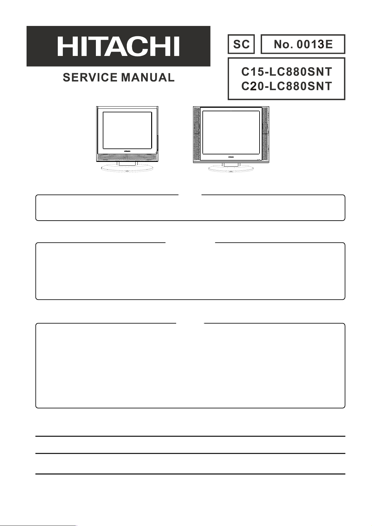
(15” model)
(20” model)
Caution
Be sure to read this manual before servicing. To assure safety from fire, electric shock, injury, harmful radiation
and materials, various measures are provided in this Hitachi liquid crystal television/monitor.
Be sure to read the cautionary items described in the manual to maintain safety before servicing.
Service Warning
1.The LCD Panel Module is made of glass. When handling broken LCD Panel Module, take special care not to
be injured.
2.Replacement work should only start after the LCD Panel Module and the AC/DC Power Supply has become
sufficiently cool.
3.Take special care of the LCD display panel and do not damage its surface.
4.Do not touch the LCD Panel Module with your bare hands and protect its surface from stains.
5.It is recommended to use clean soft gloves during servicing in order to protect the LCD display panel and the
service personnel himself.
Contents
* SAFETY NOTICE...................................................2
* DISPLAY MODES..................................................2
* SPECIFICATIONS...................................................3
* LOCATION OF CONTROLS......................................4
* CONNECTIONS......................................................7
* FACTORY SETTTINGS...........................................10
* TROUBLESHOOTING..............................................11
* SCHEMATIC DIAGRAMS.............................................12
* PRINTED CIRCUIT BOARD........................................21
* BLOCK DIAGRAM...............................................27
* WIRING DIAGRAM.............................................28
* EXPLODED VIEW & MECHANICAL PARTS LIST..........29
* INFORMATION OF ICS...............................................31
* REPLACEMENT PARTS LIST................................43
* PARTS LIST (FOR REFERENCE ONLY)...............44
SPECIFICATIONS AND PARTS ARE SUBJECT TO CHANGE FOR IMPROVEMENT
Liquid Crystal Display Television/Monitor
July 2005 Digital Media Systems Group, Hitachi Asia Ltd.
Page 2
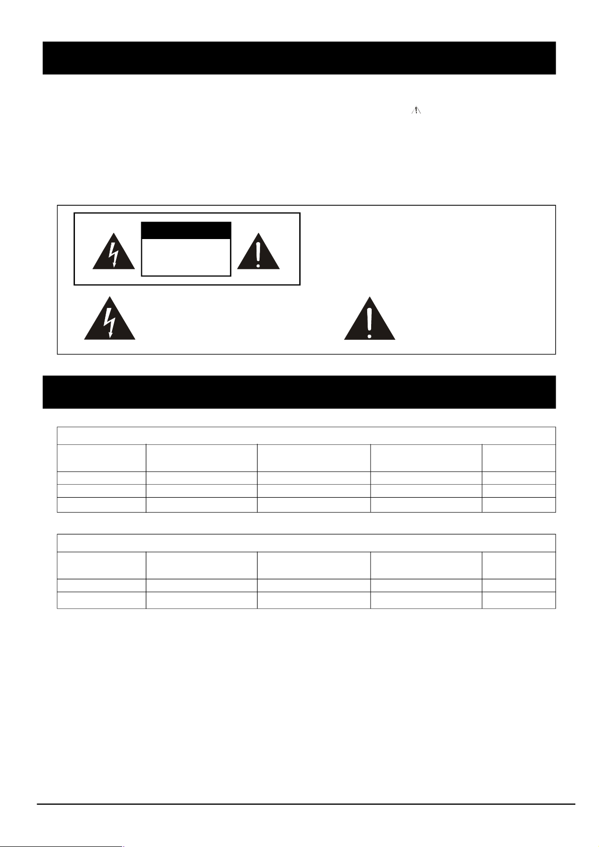
SAFETY NOTICE
Maintenance and repair of this LCD TV/monitor should be done by qualified service personnel only.
Critical parts that have special safety characteristics are identified by a in the replacement parts
list. Use of any substitute replacement part that does not have the same safety characteristics as
the recommended replacement part in the parts list might create shock, fire and / or other hazards.
Read and comply with all caution and safety related notes on or inside the LCD/monitor cabinet, the
printed circuit boards or the LCD Panel Module. Please note the following safety symbols indicated
below.
CAUTION
RISK OF ELECTRIC
SHOCK DO NOT
OPEN
This symbol indicates “dangerous
voltage” inside the product that
presents a risk of electric shock or
personal injury.
DISPLAY MODES
Resolution
640 x 480
800 x 600
1024 x 768
Horizontal
Frequency (KHz)
31.47 (N)
37.88 (P)
48.36 (N)
TO REDUCE THE RISK OF ELECTRIC SHOCK,
DO NOT REMOVE COVER.
NO USER-SERVICEABLE PARTS INSIDE.
REFER SERVICING TO QUALIFIED SERVICE
PERSONNEL.
15” Incoming display mode (input)
Vertical
Pixel Frequency
Frequency (Hz)
60.00 (N)
60.32 (P)
60.00 (N)
This symbol indicates
important instructions
accompanying the
product.
(MHz)
25.18
40.00
65.00
Comment
DOS
VESA
VESA
20” Incoming display mode (input)
Resolution
640 x 480
800 x 600
Horizontal
Frequency (KHz)
31.47 (N)
37.88 (P)
Vertical
Frequency (Hz)
60.00 (N)
60.32 (P)
Pixel Frequency
(MHz)
25.18
40.00
Comment
DOS
VESA
* Modes, which are not listed in the above table, may not be supported. For an optimal picture it is
recommended to choose a mode listed in the table.
* For 15”model, there are 3 types of incoming display modes compatible with Windows as shown
in the tables above.
* For 20”model, there are 2 types of incoming display modes compatible with Windows as shown
in the table above.
* Sometimes, the image may be disrupted due to the frequency standard from the VGA card.
However, this is not an error. You may improve this situation by activating the automatic adjustment
or by manually changing the phase and the clock settings in the menu.
* If you switch off the TV/monitor, interference lines may occur on your screen. Please note that
this is normal.
* To extend the service life of the product, we recommend that you use your computer’s power
management function.
- 2 -
Page 3
SPECIFICATIONS
Model C15-LC880SNT C20-LC880SNT
Panel
Size
Display Size
Pixel Pitch
Viewing Angle (H/V)
Screen Tilt Angle
Frequency
Horizontal
Vertical
Contrast Ratio
Brightness
Display Color
Display Resolution Optimum Mode
Maximum Mode
Input Signal Sync.
Video Signal
RGB Signal
TV / Video Color System
Sound System
Video Format
Power Supply Input
Output (Adapter)
Power Consumption
Typical
Power Saving
15.1”
304.1(H) X 228.1(V)mm
0.297(H) X 0.297(V)mm
<140 / 125
408(H) X 306(V)mm
0.51(H) X 0.51(V)mm
<160 / 140
Front 5 / Rear 15
30 ~ 70KHz
50 ~ 75Hz
400:1
400 cd/m
16.2Million
1024 X 768 @ 70Hz
1024 X 768 @ 75Hz
2
500 cd/m
16.7Million
800 X 600 @ 70Hz
800 X 600 @ 75Hz
H/V Separate, TTL, P. or N.
H/V Composite, TTL, P. or N.
Sync-on-green 0.3 Vp-p, N.
1 Vp-p @ 75 ohm
0.7Vp-p @ 75 ohm
PAL / SECAM / NTSC
DK / I / BG / M
CVBS, S-VIDEO, Y/Pb/Pr
AC 100 - 240Vrms (50Hz / 60Hz)
DC 12V / 4.5A DC 12V / 5.2A
<54W
<3W
20.1”
2
<65W
<3W
Dimensions (WxHxD)
Weight
Environmental Considerations
Operating Temperature
390 X 401 X 188mm
5.3Kg
50 to 104 (10 to 40 )
Operatiing Humidity
Storage Temperature
13 to 113 (-25 to 45 )
Storage Humidity
Audio Characteristics
Audio Input
Frequency
Response
RCA Jack Red(R) White(L), 0.5 0.3Vrms
RF: 100Hz ~ 12KHz (at 3dB)
AV : 100Hz ~ 13KHz (at 3dB)
Note:
* Design and specifications are subject to change without notice.
* Weight and dimensions shown are approximate values only.
552 X 460 X 188mm
8.4Kg
10% to 80%
5% to 95%
- 3 -
Page 4
LOCATION OF CONTROL (Continued)
LOCATION OF CONTROL
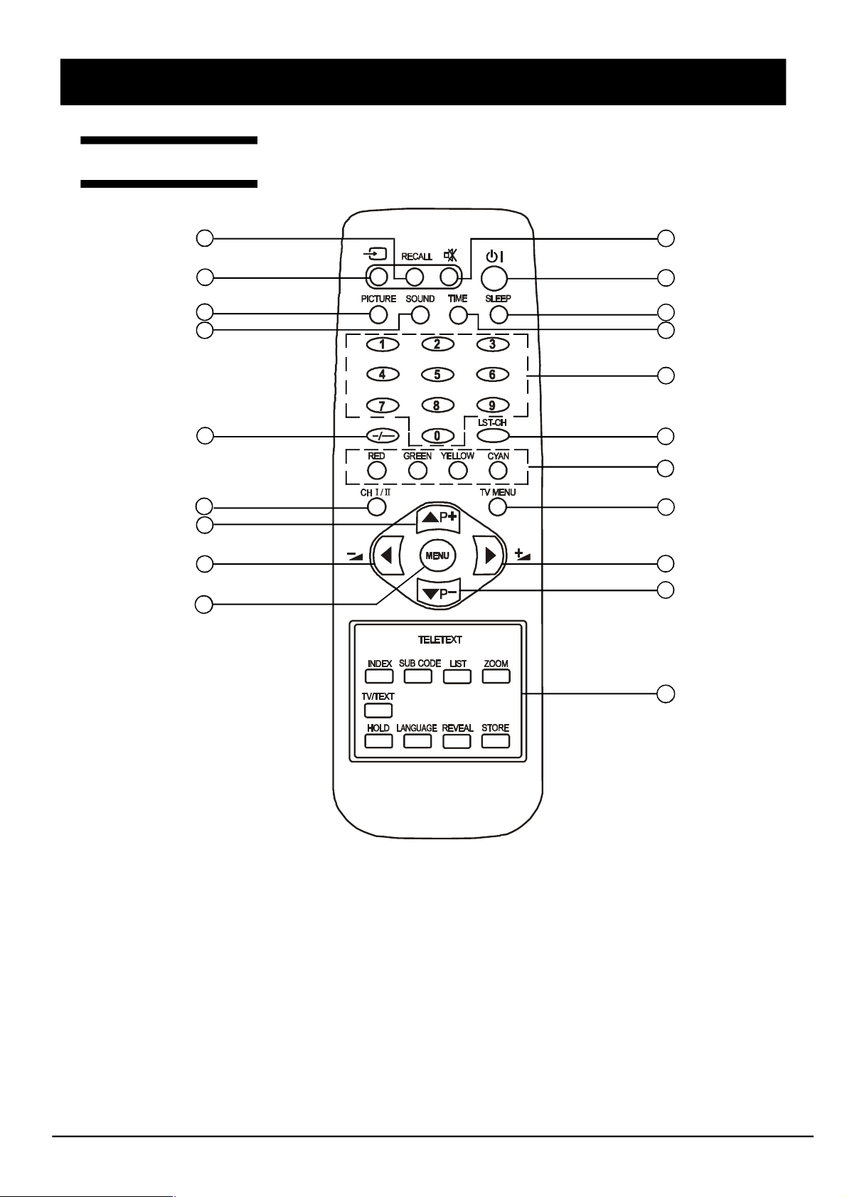
Remote Control
1 2
10
13
15
16
17
3
5
7
4
6
8
9
11
12
14
16
15
1.RECALL button
To display setup information of channel
2.MUTE button
To switch on/off sound mute
3.TV/VIDEO button
To select TV, AV1, AV2, S-Video, COMP, VGA or DVI mode
4.STANDBY button
To switch on the LCD TV/monitor when at standby mode or vice versa
5.PICTURE button
To select picture effect mode (Standard/Soft/Custom/Bright)
6.SLEEP button
To on/off sleep mode and set the sleep timer
12
- 4 -
Page 5

LOCATION OF CONTROL
7.SOUND button
To select the sound effect mode (Custom/News/Cinema/MusicHall)
8.TIME button
To display the preset time
9.NUMBER buttons
To directly select program number
10.DIGIT button
To select one, two or three-digit program number input options
11.LST-CH button
To return to previously selected program number
12.TELETEXT buttons (OPTIONAL)
These buttons are used for certain models with Teletext functions only. For further details, refer
to the “TELETEXT FUNCTION” section in this manual
13.CH I/II button
To switch between NICAM / A2 stereo and mono sound output
14.TV MENU button
To enter the TV menu directly to tune the programs
15.P-/+ ( ) buttons
To select previous / next program and to operate the menu
16. -/+ ( ) buttons
To decrease / increase volume and to adjust the menu
17.MENU button
To enter or exit from the MENU (TV/AV mode)
To accept your selection (PC mode)
- 5 -
Page 6
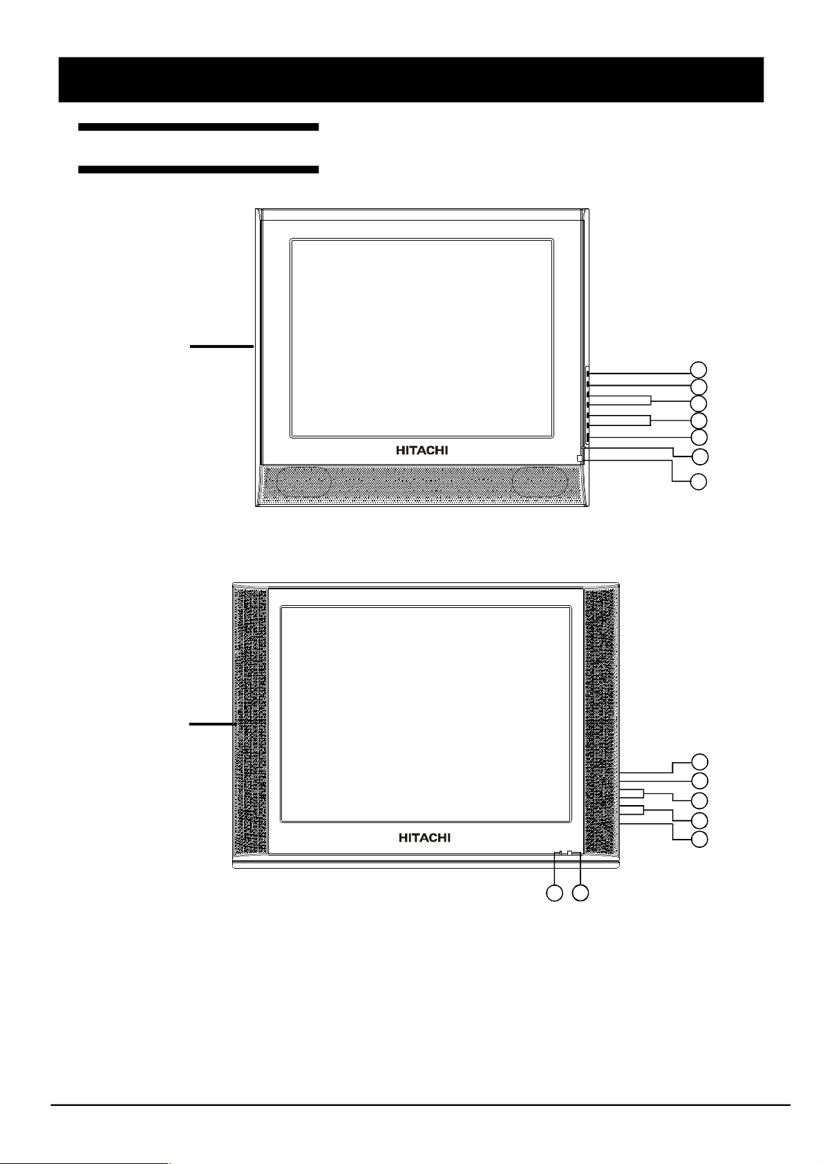
LOCATION OF CONTROL
Front and Side Panels
For 15” model
1
2
3
4
5
6
7
For 20” model
1.TV/VIDEO button
To select TV, AV1, AV2, S-Video,
COMP, VGA or DVI mode
2.MENU button
To enter or exit from the menu
3.PROGRAM buttons
To select previous/next program
4 .VOLUME buttons
To decrease/increase volume
7
6
5.STANDBY button
To switch on when at standby mode or vice
versa
6.POWER INDICATOR
Lights up in red when the set is on standby;
Lights up in green when the set is power on
7.REMOTE CONTROL SENSOR
Infrared sensor for the remote control
- 6 -
1
2
3
4
5
Page 7
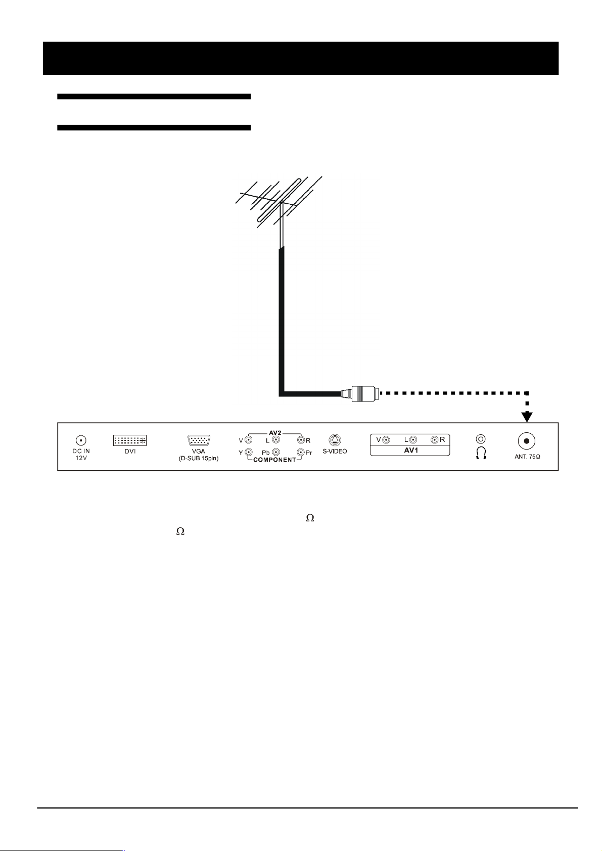
CONNECTIONS
Connecting The Antenna
Antenna
Note:
* Aerial connections: Standard-phono socket 75 or F connector..
* Input impedance: 75 unbalanced.
* For Australia only -Install an external aerial conforming to AS 1417.1 for safety purpose.
- 7 -
Page 8
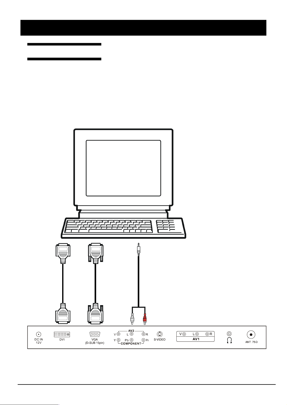
CONNECTIONS
Connecting The PC
STEPS:
1.Switch off all power supplies to the equipment and TV set before connection
2.Connect the signal and audio cables from the computer output terminal to the TV
3.Connect power cord
4.Switch on the TV first, then switch on the computer
5.If the TV still does not function properly, please refer to the troubleshooting section to diagnose
the problem.
* Please do not open the cover of the TV
T
o
D
V
I
o
u
t
p
u
t
T
o
D
V
I
i
n
p
u
t
T
(
o
D
S
-
s
i
g
u
n
b
a
)
l
o
u
t
p
u
t
T
(
o
D
S
-
s
i
g
u
n
b
a
)
l
i
n
p
u
t
T
o
A
u
d
i
o
o
u
t
p
u
t
T
(
o
A
A
V
u
2
d
)
i
o
i
n
p
u
t
Note:
Do not pull the cables. When connecting and disconnecting the cables, do it with your hand holding
the connector.
- 8 -
Page 9
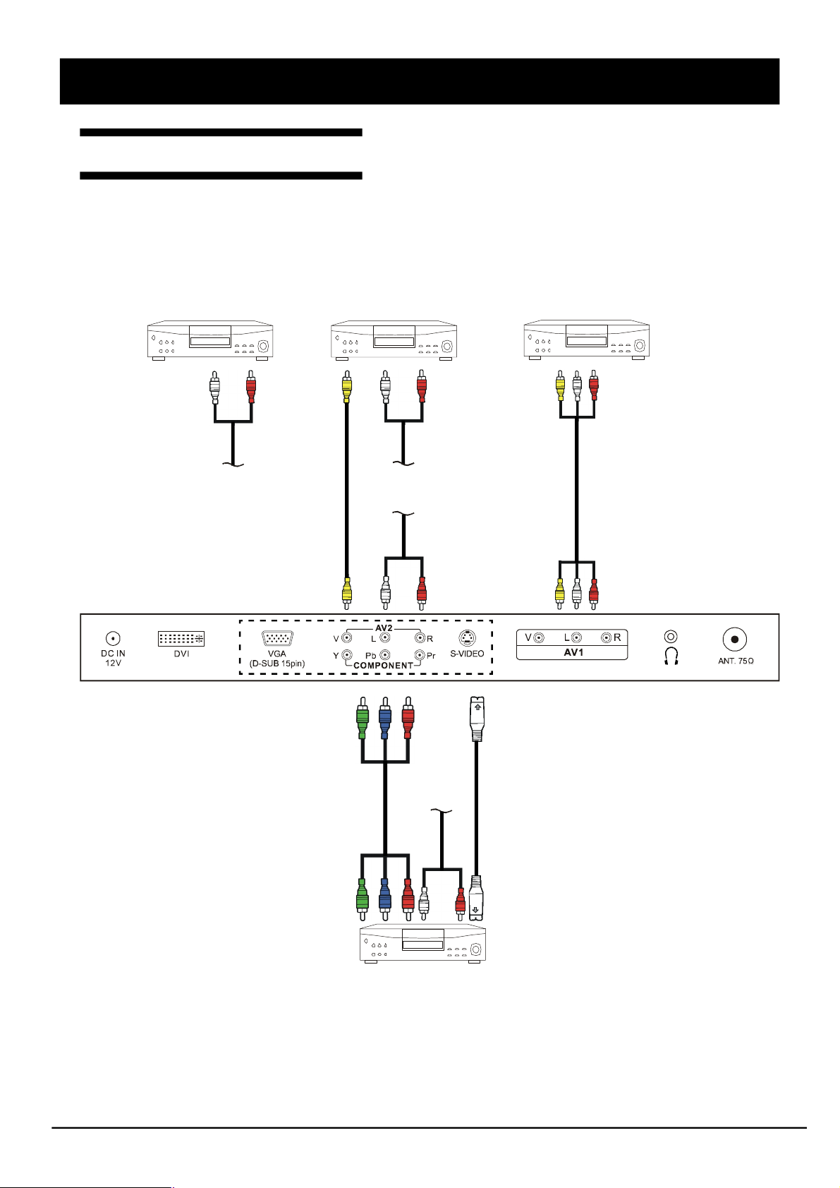
CONNECTIONS
Connecting AV Equipment
This TV set provides AV1, AV2 input terminals, S-Video and a group of Y/Pb/Pr terminal for connection
to VCR, VCD, DVD or other video equipment.
Please refer to the instruction manual of the other equipment for more information on the connection
to the TV.
’
VIDEO EQUIPMENT
To Audio
input (AV2)
VIDEO EQUIPMENT VIDEO EQUIPMENT
T
o
A
u
d
i
o
o
u
t
p
u
t
T
o
V
i
d
e
o
o
u
t
p
u
t
T
o
V
i
d
e
o
i
n
p
u
t
i
n
p
u
t
T
o
C
o
m
p
o
n
e
n
t
To Audio
input (AV2)
T
o
A
u
d
i
o
o
u
t
p
u
t
T
(
A
o
V
A
2
u
)
d
i
o
i
n
p
u
t
To Audio
input (AV2)
T
A
o
u
d
V
i
o
i
d
e
o
o
u
t
p
a
n
u
d
t
T
A
o
u
d
V
i
o
i
d
i
e
n
o
p
u
a
t
n
d
T
i
n
o
p
u
S
t
-
V
i
d
e
o
T
o
o
u
t
p
C
u
o
t
m
p
o
n
e
n
t
T
o
o
u
t
p
S
u
-
V
t
i
d
e
o
VIDEO EQUIPMENT
Note:
* Please disconnect all the power supplies to the equipment and TV set before connection.
* Do not pull the cables. When connecting and disconnecting the cables, do it with your hand
holding the connector.
* Only 1 set of audio cable is to be connected to Audio input terminals of AV2.
- 9 -
Page 10
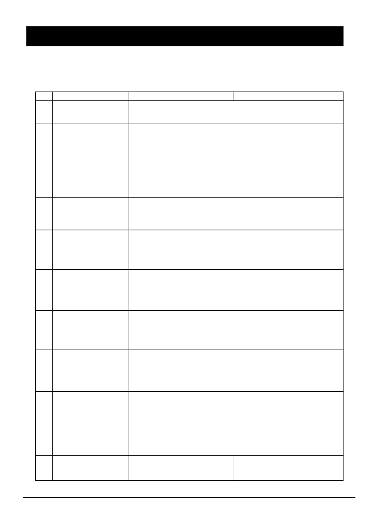
FACTORY SETTINGS
1.Press MENU button, then press 3210 using the number button on the remote control to enter
into the factory setting.
2.The factory setting menu will be displayed on the screen. The following table is shown when in
AV mode:
Item Factory setting C15-LC880SNT C20-LC880SNT
1 Basic Setting Backlight 50
NVRAM Addr
NVRAM Val
2 Color Setting Auto Adjust
Red 0
Green 0
Blue 0
Red Offset 0
Green Offset 0
Blue Offset 0
Min Volume 0
Max Volume 68
3 Sound Setting Dot1 X Pos 31
Dot1 Y Pos 69
Dot2 X Pos 62
Dot2 Y Pos 81
4 4200K 5000K Warm Brightness 128
Contrast 128
Red 247
Green 237
Blue 237
5 STANDARD Brightness 128
Contrast 128
Red 255
Green 255
Blue 255
6 COOL Brightness 128
Contrast 126
Red 224
Green 228
Blue 251
7 CUSTOM Brightness 128
Contrast 128
Red 255
Green 255
Blue 255
8 Advanced Setting Factory Mode 1
Power Mode 1
Panel Index 34
Decder SatHue 0
Enable Zoom 1
Enable SCART P
Enable DVI Port 1
Factory Reset
9 Version Info V1.9-C15-LC880SNT V1.9-C20-LC880SNT
ADDC:V8-L15GC1-A1D01 ADDC:V8-L20GC1-A1D01
DDDC:V8-L15GC1-A1D02 DDDC:V8-L20GC1-A1D02
1 1
- 10 -
Page 11
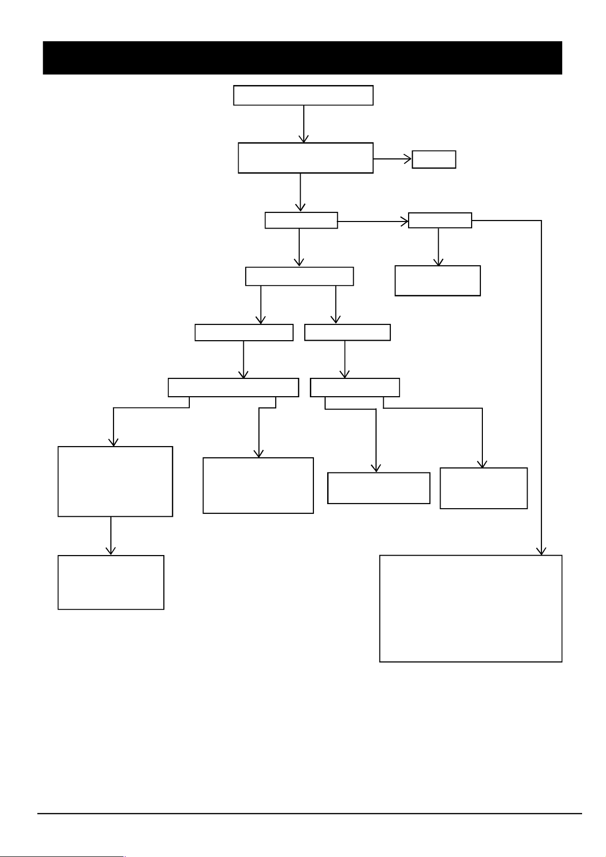
TROUBLESHOOTING
TV DOES NOT TURN ON
Normal
1.Check MCU (U4)
2.Check CN3 (or
CN7) is connected
3.Check U8 has
VCC voltage
Is the power cord and
DC adapter plugged in?
Yes
LED lights up
Yes
Press Power button
LED light is green
Check inverter PWB unit Check MCU(U4)
Defective
1.Connect the line
of J9and inverter
2.Replace inverter
with a newone
LED light is red
Defective
Replace MCU with
a new one
No
No
Plug in
Check LED
Defective
Replace LED
with a new one
Normal
Replace DRIVE
PWB unit with
a new one
Normal
Defective
1.Replace MCU
with a newone.
2.Replace U8
with a newone.
Check power input system
1.AC adapter
*Normal?
*Connected properly?
2.U9 has +5V?
3.U10 has 3.3V?
4.LED controls electrocircuit?
5.JD3 and JD2 are connected?
- 11 -
Page 12
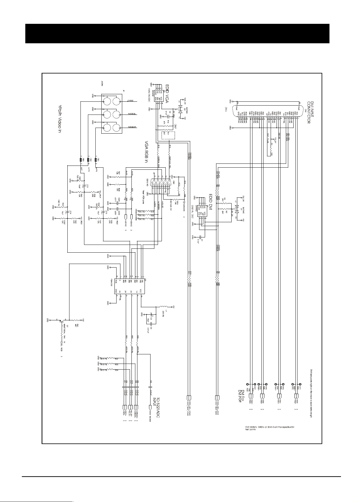
SCHEMATIC DIAGRAMS
Main Diagram-1
- 12 -
Page 13
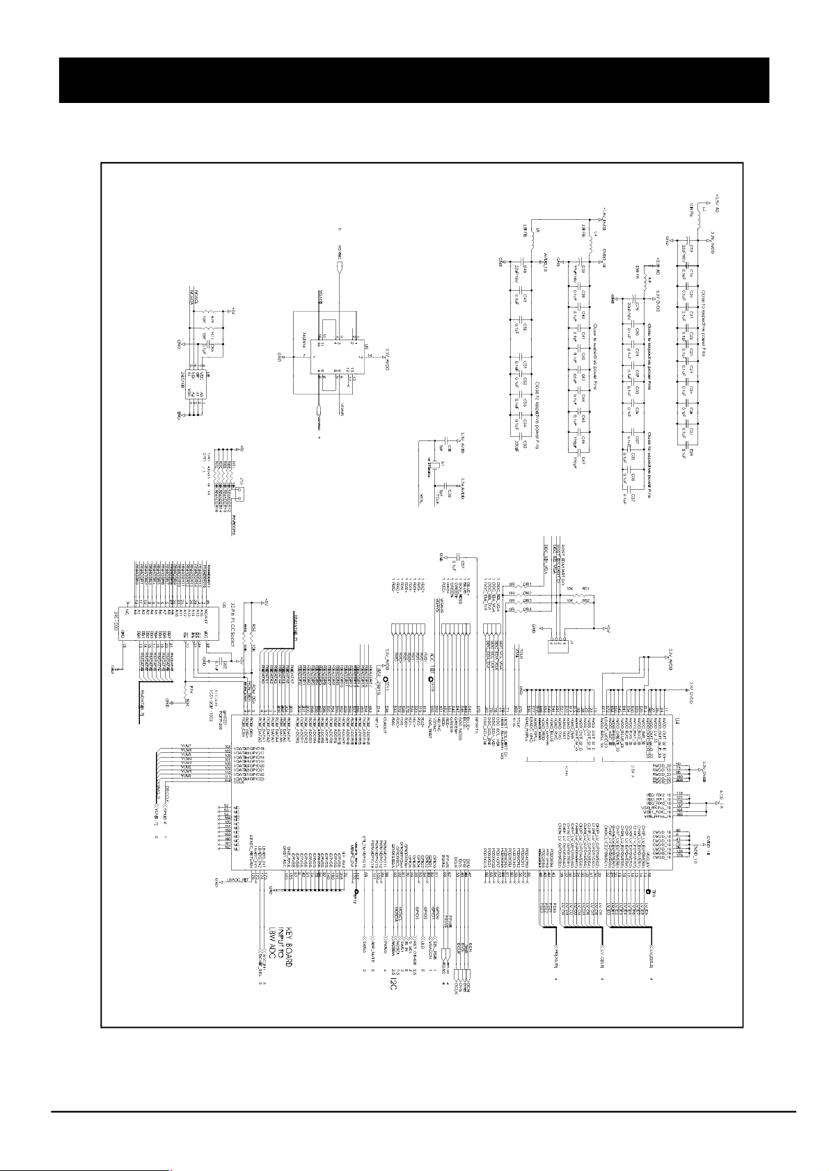
SCHEMATIC DIAGRAMS
Main Diagram-2
- 13 -
Page 14
SCHEMATIC DIAGRAMS
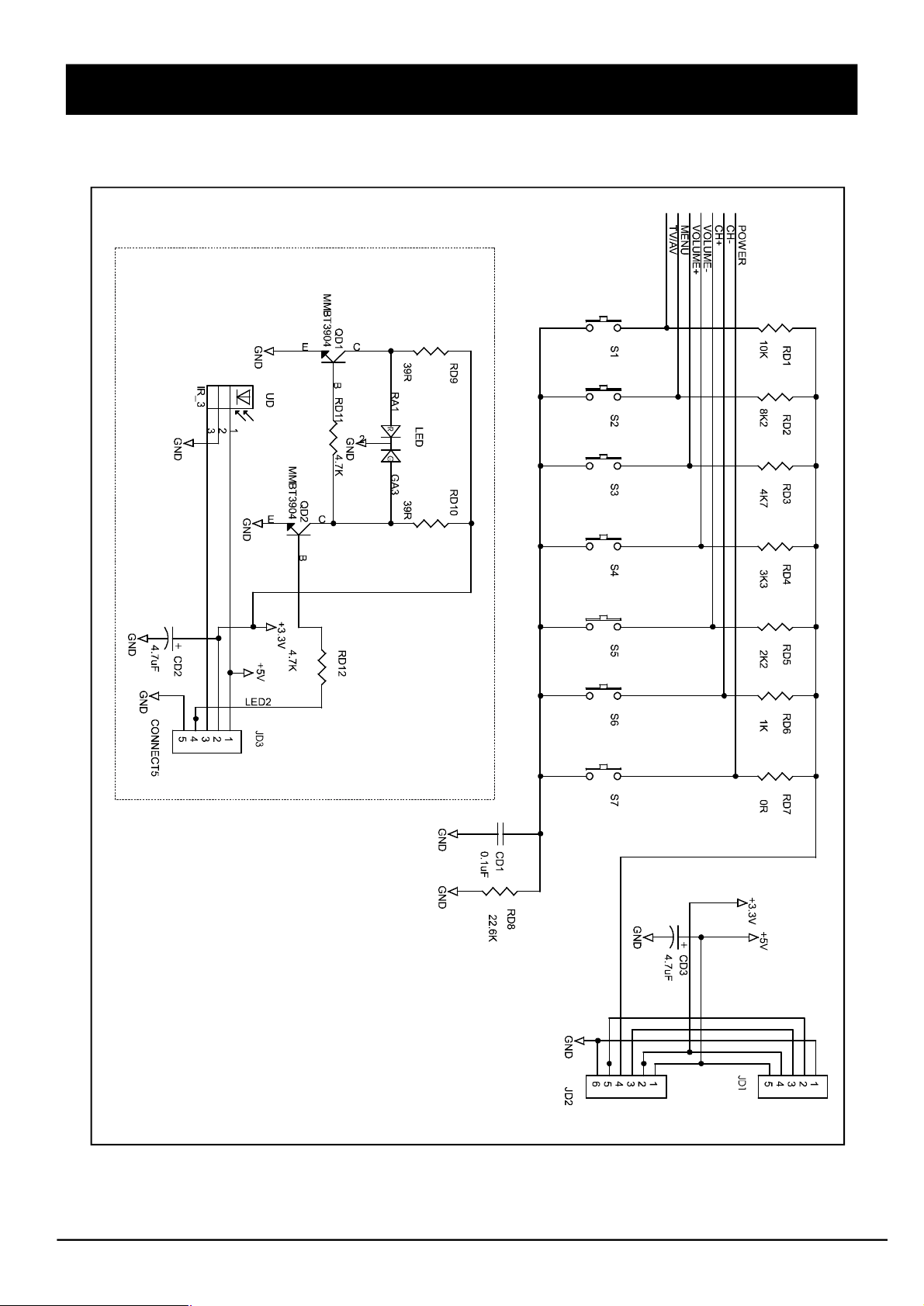
Control Keys Diagram
- 14 -
Page 15
SCHEMATIC DIAGRAMS
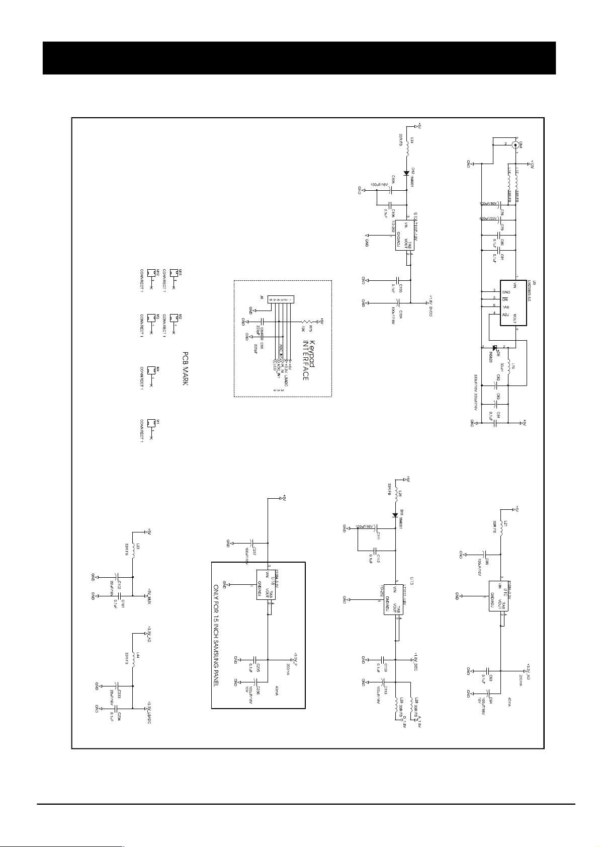
Power Diagram
- 15 -
Page 16
SCHEMATIC DIAGRAMS
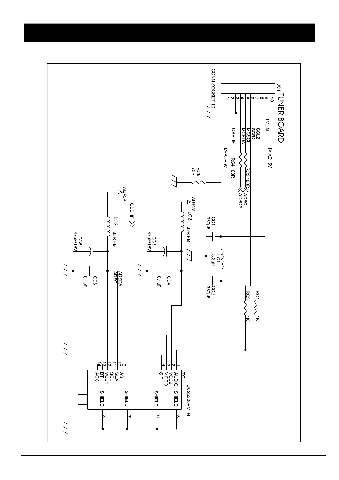
Tuner Diagram
- 16 -
Page 17

SCHEMATIC DIAGRAMS
Teletext Diagram
- 17 -
Page 18

SCHEMATIC DIAGRAMS
Video Decoder Diagram
- 18 -
Page 19

SCHEMATIC DIAGRAMS
Audio And CONN Diagram
- 19 -
Page 20

SCHEMATIC DIAGRAMS
Lvds_ttl-out Diagram
- 20 -
Page 21

PRINTED CIRCUIT BOARD
Main Board (Top Side)
- 21 -
Page 22

PRINTED CIRCUIT BOARD
Main Board (Bottom Side)
- 22 -
Page 23

PRINTED CIRCUIT BOARD
Control Keys Board (Top Side)
- 23 -
Page 24

PRINTED CIRCUIT BOARD
Control Keys Board (Bottom Side)
- 24 -
Page 25

PRINTED CIRCUIT BOARD
Tuner Board (Top Side)
- 25 -
Page 26

PRINTED CIRCUIT BOARD
Tuner Board (Bottom Side)
- 26 -
Page 27

BLOCK DIAGRAM
- 27 -
Page 28

WIRING DIAGRAM
- 28 -
Page 29

EXPLODED VIEW & MECHANICAL PARTS LIST
For 15” model
- 29 -
Page 30

EXPLODED VIEW & MECHANICAL PARTS LIST
For 20” model
- 30 -
Page 31

INFORMATION OF ICS
IC MC78M05 D-PAK
Pin No. Pin Name Description Pin No. Pin Name Description
1 Input Output Voltage 3 Output Output Voltage
2 GND
IC LM1117DTX-3.3 TO-252
Pin No. Pin Name Description Pin No. Pin Name Description
1 Input Output Voltage 3 Adi/GND Output Voltage
2 Output
IC LM1084ISX-3.3 TO263
Pin No. Pin Name Description Pin No. Pin Name Description
1 Input Output Voltage 3 Adi/GND Output Voltage
2 Output
IC LM2596S-5.0 TO-263
Pin No. Pin Name Description Pin No. Pin Name Description
1 VIN 4 Feed Back
2 Output 5 ON/OFF
3 Ground
IC SN74CBT3253CDBQR SSOP16
Pin No. Pin Name Description Pin No. Pin Name Description
1 1OE 9 2A
2 S1 10 2B1
3 1B4 11 2B2
4 1B3 12 2B3
5 1B2 13 2B4
6 1B1 14 S0
7 1A 15 2OE
8 GND 16 VCC
IC24LC16BT SOIC08
Pin No. Pin Name Description Pin No. Pin Name Description
1 A0 5 SDA
2 A1 6 SCL
3 A2 7 WP
4 VSS 8 VCC
IC FDS9933A SO-8
Pin No. Pin Name Description Pin No. Pin Name Description
1 S1 Source Voltage 5 D2 Drain-Source Voltage
2 G1 Gate-Source Voltage 6 D2 Drain-Source Voltage
3 S2 Source Voltage 7 D1 Drain-Source Voltage
4 G2 Gate-Source Voltage 8 D1 Drain-Source Voltage
IC 24AA02 SOIC08
Pin No. Pin Name Description Pin No. Pin Name Description
1 A0 5 SDA
2 A1 6 SCL
3 A2 7 WP
4 VSS 8 VCC
- 31 -
Page 32

INFORMATION OF ICS
IC FSAV330 QS0P16
Pin No. Pin Name Description Pin No. Pin Name Description
1 S 9 3A
2 1B 1 10 3B2
3 1B2 11 3B1
4 1A 12 4A
5 2B 1 13 4B2
6 2B2 14 4B1
7 2A 15 OE
8 GND 16 VCC
IC 74LCX14 S0IC14
Pin No. Pin Name Description Pin No. Pin Name Description
1 I0 Inputs 8 O3 Outputs
2 O0 Outputs 9 I3 Inputs
3 I1 Inputs 10 O4 Outputs
4 O1 Outputs 11 I4 Inputs
5 I2 Inputs 12 O5 Outputs
6 O2 Outputs 13 I5 Inputs
7 GND Inputs 14 VCC
IC SST39SF020A PLCC32
Pin No. Pin Name Description Pin No. Pin Name Description
1 AMS1- A0 Address Inputs 5 WE# Write Enable
2 DQ7-DQ0 Data Input/output 6 VDD Power Supply
3 CE# Chip Enable 7 VSS Ground
4 OE# Output Enable 8 NC No Connection
IC GM5221 PQFP-208 (DVI Input Port)
Pin No. Pin Name Description
113 AVDD_IMB_3.3 Analog VDD(3.3V) for internal biasing gircuits. Must be bypassed with
capacitors
114 REXT External termination resistor.
A 1% 250Ω, resistor should by connected from this pin to AVDD_IMB
115 AGND_IMB Analog GND for internal biasing circuits. Must be connected directly to
the ground plane.
116 VDD_RX2_1.8 VDD(1.8V) for TMDS input pair 2.
Must be bypassed with external capacitor to GND_RX2.
117 AGMD_RX2 Analog GND for TMDS input pair 2. Must be connected directly to the
analog ground plane.
118 RX2+ TMDS input pair2
119 RX2- TMDS input pair2
120 AVDD_RX2_3.3 Analog VDD(3.3V) for TMDS input pair 2. Must be bypassed with
capacitor to AGND_RX2.
121 VDD_RX1_1.8 VDD(1.8V) for TMDS input pair 2. Must be bypassed with external
capacitor to GND_RX1.
122 AGND_RX1 Analog GND for TMDS input pair 1. Must be connected directly to the
analog ground plane.
123 RX1+ TMDS input pair 1
124 RX- TMDS input pair 1
125 AVDD_RX1_3.3 Analog VDD (3.3V) for TMDS input pair 2. Must be bypassed with to
AGND_RX1.
- 32 -
Page 33

INFORMATION OF ICS
IC GM5221 PQFP-208 (DVI Input Port)
Pin No. Pin Name Description
126 VDD_RX0_1.8 VDD (1.8V) for TMDS input pair 2. Must be bypassed with external
capacitor to GND_RX0
127 AGND_RX0 Analog GND for TMDS input pair 0. Must be connected directly to the
analog ground plane.
128 RX0+ TMDS input pair 0
129 RX0- TMDS input pair 0
130 AVDD_RX0_3.3 Analog VDD (3.3V) for TMDS input pair 2. Must be bypassed with
capacitor to AGND_RX0
131 AGND_RXC Analog GND for TMDS input clock pair. Must be connected directly to
the analog ground plane.
132 RXC+ TMDS input clock pair
133 RXC- TMDS input clock pair
134 AVDD_RXC_3.3 Analog VDD (3.3V) for TMDS input clock pair.
Must be bypassed with 100pF capacitor to AGND_RXC.
136 GND_RXPLL Analog GND for the TMDS receiver internal PLL.
Must be connected directly to the analog ground plane.
137 VDD_RXPLL_1.8Analog VDD (1.8V) for the TMDS receiver internal PLL.
Must be bypassed with a capacitor to AGND_RXPLL.
138 CLK_OUT Reserved, unconnected.
IC GM5221 PQFP-208 (RCLK PLL Pins)
Pin No. Pin Name Description
165 GND_RPLL Digital GND for ADC clocking circuit. Must be directly connected to the
digital system ground plane.
166 VDD_RPLL_1.8 Digital power (1.8V) for ADC digital logic. Must be bypassed with
capacitor to GND1_ADC.
168 AGND_RPLL Analog ground for the Reference DDS PLL. Must be directly connected
to the analog system ground plane.
169 XTAL Crystal oscillator output.
170 TCLK Reference clock (TCLK) from the 14.3MHz crystal oscillator.
171 AVDD_RPLL_3.3 Analog VDD (3.3V)
IC GM5221 PQFP-208 (Input Video Port)
Pin No. Pin Name Description
112 VCLK Video port data clock input. Up to 75Mhz
[Input, 5V-tolerant]
111 GPIO23/VDATA0 Input YUV data in 8-bit BT656 or GPIO23:16 if VPORT is disabled.
110 GPIO22/VDATA1 [Bi-Directional, 5V-tolerant]
109 GPIO21/VDATA2
108 GPIO20/VDATA3
107 GPIO19/VDATA4
106 GPIO18/VDATA5
103 GPIO17/VDATA6
102 GPIO16/VDATA7
- 33 -
Page 34

INFORMATION OF ICS
IC GM5221 PQFP-208 (Analog Input Port)
Pin No. Pin Name Description
141 AVDD_BLUE_3.3Analog power (3.3V) for the blue channel. Must be bypassed with
capacitor to AGND_BLUE pin on system board.
142 BLUE+ Positive analog input for Blue channel.
143 BLUE- Negative analog input for Blue channel.
144 AGND_BLUE Analog ground for the blue channel. Must be directly connected to the
analog system ground plane.
145 AVDD_GREEN_3.3 Analog power (3.3V) for the green channel. Must be bypassed with
capacitor to AGND_GREEN pin on system board.
146 SOG_MCSS Dedicated Sync-on-Green pin.
NOTE: This pin requires the same AC-couple capacitor (if applicable)
like the regular RGB input pins.
147 GREEN+ Positive analog input for Green channel.
148 GREEN- Negative analog input for Green channel.
NOTE: For SOG support this pin should be pulled down to GND
through a 1MΩ, resistor.
149 AGND_GREEN Analog ground for the green channel. Must be directly connected to the
analog system ground plane.
150 AVDD_RED_3.3 Analog power (3.3V) for the red channel. Must be bypassed with
capacitor to AGND_RED pin on system board.
151 RED+ Positive analog input for Red channel.
152 RED- Negative analog input for Red channel.
153 AGND_RED Analog ground for the red channel. Must be directly connected to the
analog system ground plane.
154 AVDD_ADC_3.3 Analog power (3.3V) for ADC Analog blocks that are shared by all three
channels. Includes bandgap reference, master biasing and full scale
adjust. Must be bypassed with capacitor th AGND_ADC pin on system
board.
156 AGND_ADC Analog ground for ADC analog blocks that are shared by all three
channels. Includes bandgap reference, master biasing and full scale
adjust. Must be directly connected to analog system ground plane.
163 GND1_ADC Digital GND for ADC clocking circuit. Must be directly connected to the
digital system ground plane.
164 VDD1_ADC_1.8 Digital power (1.8V) for ADC encoding logic. Must be bypassed with
capacitor to GND1_ADC pin on system board.
181 HSYNC/CSYNC ADC input horizontal sync or composite sync input.
[Input, Schmitt trigger with 1V hysteresis and 1.65V threshold. 5V-tolerant]
182 VSYNC ADC input vertical sync.
[Input, Schmitt trigger with 1V hysteresis and 1.65V threshold. 5V-tolerant]
- 34 -
Page 35

INFORMATION OF ICS
IC GM5221 PQFP-208 (System Interface)
Pin No. Pin Name Description
81 GPIO0 General-purpose input/output signals
82 GPIO1 [Bi-directional, Schmitt trigger, 5V-tolerant]
83 GPIO2
84 GPIO3
85 GPIO4
88 GPIO5
89 GPIO6
90 GPIO7/IRQin General-purpose input/output signals [Bi-directional, Schmitt trigger, 5V91 GPIO8/IRQout tolerant] or OCM interrupt and chip status.
92 GPIO9/SCL General-purpose input/output signals [Bi-directional, Schmitt trigger, 5V93 GPIO10/SDA tolerant] or master device on serial interface bus.
98 GPIO11/PWM0 General-purpose input/output signals or PWM signals. [Bi-directional,
99 GPIO12/PWM1 Schmitt trigger, 5V-tolerant]
100 GPIO13/PWM2
101 GPIO14/PWM3
69 GPIO15 General-purpose input/output signals [Bi-directional, Schmitt trigger, 5V-tolerant]
77 DDC_SCL_VGA DDC2Bi clock for VGA Port
78 DDC_SDA_VGA DDC2Bi data for VGA Port [internal 10KΩ, pull-up resistor]
79 DDC_SCL_DVI DDC2Bi and HDCP clock for DVI Port
80 DDC_SDA_DVD DC2Bi and HDCP data for DVI Port [internal 10KΩ, pull-up resistor]
178 RESETn Hardware Reset (active low) [Schmitt trigger, 5V-tolerant] Connect to
ground with 0.01uF (or larger) capacitor. See section, Chip
Initialization, for detail
172 LBADC_VDD_3.3 Analog 3.3V power supply for general-purpose ADC
173 LBADC_IN1 LBADC channel 1
174 LBADC_IN2 LBADC channel 2
175 LBADC_IN3 LBADC channel 3
176 LBADC_RETURN Analog Ground (signal return path) for LBADC channels 1, 2 and 3
177 LBADC_GND Ground
71 HOST_SCL/UART_DI Host input clock or 186 UART Data In or JTAG clock signal. [Input,
Schmitt trigger, 5V-Tolerant]
72 HOST_SCL/UART_DO Host input data or 186 UART Data out or JTAG mode signal.
[Bi-directional, Schmitt trigger, slew rate limited, 5V-Tolerant]
66 JTAG_TDIJTAG Data input signal.
64 JTAG_TDO JTAG data output signal.
56 JTAG_RESET JTAG reset signal.
- 35 -
Page 36

INFORMATION OF ICS
IC GM5221 PQFP-208 (LVDS Display Interface)
Pin No. Pin Name Description
11 AVDD_LV_E_3.3 Digital Power for LVDS outputs. Connect to digital 3.3V supply.
12 AVSS_LV_E Ground for LVDS outputs.
13 CH3P_LV_E
14 CH3N_LV_E
15 CLKP_LV_E
16 CLKN_LV_E
17 CH2P_LV_E
18 CH2N_LV_E
19 CH1P_LV_E
20 CH1N_LV_E
21 CH0P_LV_E
22 CH0N_LV_E
23 AVSS_LV_E Ground for LVDS outputs.
24 AVDD_LV_E_3.3 Digital Power for LVDS outputs. Connect to digital 3.3V supply.
25 AVSS_LV Ground for LVDS outputs.
26 AVDD_LV_3.3 Analog Power for LVDS outputs. Connect to analog 3.3V supply.
27 AVDD_LV_O_3.3 Digital Power for LVDS outputs. Connect to digital 3.3V supply.
28 AVSS_LV_O Ground for LVDS outputs.
29 CH3P_LV_O
30 CH3N_LV_O
31 CLKP_LV_O
32 CLKN_LV_O
33 CH2P_LV_O
34 CH2N_LV_O
35 CH1P_LV_O
36 CH1N_LV_O
37 CH0P_LV_O
38 CH0N_LV_O
39 AVSS_LV_O Ground for LVDS outputs.
40 AVDD_LV_O_3.3 Digital Power for LVDS outputs. Connect to digital 3.3V supply.
67 PPWR Panel Power Control [Tri-state output, 5V-tolerant]
68 PBIAS PANEL Bias Control (backlight enable) [Tri-state output, 5V- tolerant]
43 RESERVED Reserved, unconnected.
44 RESERVED Reserved, unconnected.
45 RESERVED Reserved, unconnected.
46 RESERVED Reserved, unconnected.
47 RESERVED Reserved, unconnected. (Display Enable for TTL interface)
48 RESERVED Reserved, unconnected. (Display Horizontal Sync for TTL interface)
49 RESERVED Reserved, unconnected. (Display Vertical Sync for TTL interface)
- 36 -
Page 37

INFORMATION OF ICS
IC GM5221 PQFP-208 (TTL Display Interface)
Pin No. Pin Name Description
11 AVDD_LV_E_3.3 Analog Power for TTL outputs. Connect to analog 3.3V supply
12 AVSS_LV_E Ground
13 ER0 Red channel bit 0 Not used.
14 ER1 Red channel bit 1 Not used.
15 ER2 Red channel bit 2 Red channel bit 0
16 ER3 Red channel bit 3 Red channel bit 1
17 ER4 Red channel bit 4 Red channel bit 2
18 ER5 Red channel bit 5 Red channel bit 3
19 ER6 Red channel bit 6 Red channel bit 4
20 ER7 Red channel bit 7 Red channel bit 5
21 EG0 Green channel bit 0 Not used.
22 EG1 Green channel bit 1 Not used.
23 AVSS_LV_E Ground for TTL outputs.
24 AVDD_LV_E_3.3 Digital Power for TTL outputs. Connect to digital 3.3V supply.
25 AVSS_LV Ground for TTL outputs.
26 AVDD_LV_3.3 Digital Power for TTL outputs. Connect to digital 3.3V supply.
27 AVDD_LV_O_3.3 Digital Power for TTL outputs. Connect to digital 3.3V supply.
28 AVSS_LV_O Ground for TTL outputs.
29 EG2 Green channel bit 2 Green channel bit 0
30 EG3 Green channel bit 3 Green channel bit 1
31 EG4 Green channel bit 4 Green channel bit 2
32 EG5 Green channel bit 5 Green channel bit 3
33 EG6 Green channel bit 6 Green channel bit 4
34 EG7 Green channel bit 7 Green channel bit 5
35 EB0 Blue channel bit 0 Not used.
36 EB1 Blue channel bit 1 Not used.
37 EB2 Blue channel bit 2 Blue channel bit 0
38 EB3 Blue channel bit 3 Blue channel bit 1
39 AVSS_LV_O Ground
40 AVDD_LV_O_3.3 Digital Power for TTL outputs. Connect to digital 3.3V supply.
43 EB4 Blue channel bit 4 Blue channel bit 2
44 EB5 Blue channel bit 5 Blue channel bit 3
45 EB6 Blue channel bit 6 Blue channel bit 4
46 EB7 Blue channel bit 7 Blue channel bit 5
47 DEN Display Enable
48 DHS Display Horizontal Sync.
49 DVS Display Vertical Sync.
55 DCLK Display Pixel Clock.
67 PPWR Panel Power Control [Tri-state output, 5V-tolerant]
68 PBIAS Panel Bias Control (backlight enable) [Tri-state output, 5V-tolerant]
- 37 -
Page 38

INFORMATION OF ICS
IC GM5221 PQFP-208 (Miscellaneous)
Pin No. Pin Name Description
1 ROM-DATA3 External ROM DATA3
2 ROM-DATA2 External ROM DATA2
3 ROM-DATA1 External ROM DATA1
4 ROM-DATA0 External ROM DATA0
5 ROM-OEn External ROM Output Enable
6 ROM-WEn External ROM Write Enable
7 ROM-CSN External ROM Crip Select Enable
8,42,51, CRVSS Ground for cord power
74,76,87,
94,97,
140,180
9,41,75, CVDD_18 Cord Digital power. Connect to digital 1.8V supply.
86,96,
139,179
10,57,58, RESERVED Reserved, unconnected
59,60,61,
62,63,65,
70,135,
155,167
50,73,95 RVDD_33 Ring VDD power. Connect to digital 3.3V supply
52,53,54, N.C. No connected
104,105,
157,158,
159,160,
161,162
- 38 -
Page 39

INFORMATION OF ICS
IC SAA5264PS/M3/0104 SDIP52
Pin No. Pin Name Description
1 PWM Output for 14-bit high precision Pulse Width Modulator(PWM)
2 PWM0 Output for 6-bit PWMs 0 to 6
3 PWM1
4 PWM2
5 PWM3
6 PWM4
7 PWM5
8 PWM6
9 ADC0 Inputs for the software Analog-to-Digital-Converter(ADC) facility
10 ADC1
11 ADC2
12 ADC3
13 VSCC Core ground
14 SCL(NVRAM) I2C-bus Serial Clock input to Non-Volatile RAM
15 SDA(NVRAM) I2C-bus Serial Data input/output (Non-Volatile RAM)
16 Input/output for general use
17 Input/output for general use
18 Input/output for general use
19 8mA current sinking capability for direct drive of Light Emitting
20 Diodes (LEDs)
21 Input/output for general use
22 VSSA Analog ground
23 CVBS0 Composite Video Baseband Signal(CVBS) input; a positive-going
24 CVBS1 1 V (peak-to peak) input is required; connected via a 100 nF capacitor
25 SYNC_FILTER Sync-pulse-filter input for CVBS; this pin should be connected to VSSA
via a 100nF capacitor
26 IREF Reference current input for analog circuits; for correct operation a
24kΩ resistor should be connected to VSSA
27 FRAME Frame de-interlace output synchronized with the VSYNC pulse to
produce a non-interlaced display by adjustment of the vertical
deflection circuits
28 TEST Not avallable; connect this pin to VSSA
29 COR Contrast reduction:open-drain, active LOW output which allows selective
contrast reduction of the TV picture to enhance a mixed mode display
30 PWM7 Output for 6-bit PWM7
31 VDDA Analog supply voltage (3.3V)
32 B Blue colour information pixel rate output
33 G Green colour information pixel rate output
34 R Red colour information pixel rate output
35 VDS Video/data switch push-pull output for pixel rate fast blanking
36 HSYNC Horizontal sync pulse input: Schmitt triggered for a Transistor Transistor
Lever(TTL) version; the polarity of this pulse is programmable by
register bit TXT1.H POLARITY
- 39 -
Page 40

INFORMATION OF ICS
IC SAA5264PS/M3/0104 SDIP52
Pin No. Pin Name Description
37 VSYNC Vertical sync pulse input; Schmitt triggered for a TTL version; the
polarity of this pulse is programmable by register bit TXT1. V POLARITY
38 VSSP Periphery ground
39 VDDC Core supply voltage (+3.3V)
40 OSCGND Crystal oscillator ground
41 XTALIN 12 MHz crystal oscillator input
42 STALOUT 12 MHz crystal oscillator output
43 RESET Reset input; if this pin is HIGH for at least 2 machine cycles (24 oscillator
periods) while the oscillator is running, the device resets; this pin
should be connected to VDDP via a capacitor
44 VDDP Periphery supply voltage (+3.3V)
45 Input/output for general use
46 Input/output for general use
47 Input/output for general use
48 Input/output for general use
49 SCL I2C-bus Serial Clock input from application
50 SDA I2C-bus Serial Data input/output (application)
51 Input/output for general use
52 Input/output for general use
IC TPA1517NE DIP20
Pin No. Pin Name Description
1 IN1 IN1 is the audio input for channel 1.
2 SGND SGND is the input signal ground reference.
3 SVRR SVRR is the midrail bypass.
4 OUT1 OUT1 is the audio output for channel1.
5 PGND PGND is the power ground reference.
6 OUT2 OUT2 is the audio output for channel 2.
7 VCC VCC is the supply voltage input.
8 M/SB M/SB is the mute/standby mode enable. When held at less than 2 V,
this signal enables the TPA1517 for standby operation. When held
between 3.5V and 8.2V,this signal enables the TPA1517 for mute
operation. When held above 9.3V, the TPA1517 operates normally.
9 IN2 IN2 in the audio input for channel 2.
10-20 GND/HS GND/HS are the ground and heatsink connections. All GND/HS
terminals are connected directly to the mount pad for thermal-enhanced
operation.
IC TVP5146PFP S-PQFP-G80 (Clock Signals)
Pin No. Pin Name Description
40 DATACLK Line-locked data output clock.
74 XTAL1 External clock reference input. it may be connected to an external
oscillator with a 1.8V compatible clock signal or a 14.31818-MHz
crystal oscillator.
75 XTAL2 External clock reference output. Not connected if XTAL1 is driven by an
external single-ended oscillator.
- 40 -
Page 41

INFORMATION OF ICS
IC TVP5146PFP S-PQFP-G80 (Analog Video)
Pin No. Pin Name Description
80 VI_1_A
1 VI_1_B VI_1_x: Analog video input for CVBS/Pb/B/C
2 VI_1_C VI_2_x: Analog video input for CVBS/Y/G
7 VI_2_A VI_3_x: Analog video input for CVBS/Pr/R/C
8 VI_2_B VI_4_x: Analog video input for CVBS/Y
9 VI_2_C Up to 10 composite, 4 S-video, and 2 composite or 3 component
16 VI_3_A video input(or a combination thereof) can be supported.
17 VI_3_B The inputs must be ac-coupled. The recommended coupling
18 VI_3_C capacitor is 0.1μF.
23 VI_4_A The possible input configurations are listed in the input select
register at I2C subaddress 00h
IC TVP5146PFP S-PQFP-G80 (Digital Video)
Pin No. Pin Name Description
57,58 C[9:0]/ Digital video output of CbCr, C[9] is MSB and C[0] is LSB. Unused
59,60, GPIO[9:0] outputs can be left unconnected. Also, these terminals can be
63,64, programmable general-purpose I/O.
65,66, For the 8-bit mode, the two LSBs are ignored.
69,70
58 D_BLUE Digital BLUE input from overlay device.
59 D_GREEN Digital GREEN input from overlay device.
60 D_RED Digital RED input from overlay device.
57 FSO Fast-switch overlay between digital RGB and any video.
43,44 Y[9:0] Digital video output of Y/YCbCr, Y[9] is MSB and Y[0] is LSB.
45,46, For the 8-bit mode, the two LSBs are ignored. Unused outputs
47,50, can be left unconnected.
51,52,
53,54
IC TVP5146PFP S-PQFP-G80 (Miscellaneous Signals)
Pin No. Pin Name Description
35 FSS/GPIO Fast-switch(blanking) input. Switching signal between the synchronous
component video(YPbPr/RGB) and the composite video input.
Programmable general-purpose I/O
37 GLCO/I2CA Genlock control output(GLCO). Two Genlock data formats are available:
TI format and real time control(RTC) format.
During reset, this terminal is an input used to program the I2C address LSB.
30 INTREQ Interrupt request
33 PWDN Power down input: 1=Power down 0=Normal mode
34 RESETB Reset input, active low
IC TVP5146PFP S-PQFP-G80 (Host Interface)
Pin No. Pin Name Description
28 SCL I2C clock input
29 SDA I2C data bus
- 41 -
Page 42

INFORMATION OF ICS
IC TVP5146PFP S-PQFP-G80 (Power Supply)
Pin No. Pin Name Description
26 AGND Analog ground. Connect to analog ground.
13 A18GND_REF Analog 1.8-V return
12 A18VDD_REF Analog power for reference 1.8V
79 CH1_A18GND
10 CH2_A18GND Analog 1.8-V return
15 CH3_A18GND
24 CH4_A18GND
78 CH1_A18GND
11 CH2_A18GND Analog power. Connect to 1.8 V.
14 CH3_A18GND
25 CH4_A18GND
3 CH1_A33GND
6 CH2_A33GND Analog 3.3-V return
19 CH3_A33GND
22 CH4_A33GND
4 CH1_A33VDD
5 CH2_A33VDD Analog power. Connect to 3.3 V.
20 CH3_A33VDD
21 CH4_A33VDD
27,32,42 DGND Digital return
56,68
31,41,55 DVDD Digital power. Connect to 1.8 V.
67
39,49,62 IOGND Digital power return
38, 48,61 IOVDD Digital power. Connect to 3.3 V or less for reduced noise.
77 PLL_A18GND Analog power return
76 PLL_A18VDD Host Interfacewer. Connect to 1.8 V.
IC TVP5146PFP S-PQFP-G80 (Sync Signals)
Pin No. Pin Name Description
72 HS/CS/GPIO Horizontal sync output or digital composite sync output Programmable
general-purpose I/O
73 VS/VBLK/GPIO Vertical sync output (for modes with dedicated VSYNC) or VBLK
output Programmable general-purpose I/O
71 FID/GPIO Odd/even field indicator output. This terminal needs a pulldown resistor.
Programmable general-purpose I/O
36 AVID/GPIO Active video indicator output
Programmable general-purpose I/O
- 42 -
Page 43

REPLACEMENT PARTS LIST
The following service parts list are available for purchase.
Serviceman may quote the components shown in this page for servicing purposes.
PRODUCT SAFETY NOTE : Critical parts that have special safety characteristics are identified by a in
the replacement parts list or the schematic diagrams. Use of any substitute replacement part that does not have
the same safety characteristics as the recommended replacement part in the parts list might create shock, fire
and/or other hazards.
Please do not degrade the safety of this TV through improper servicing.
Part No. Description
PCB ASSEMBLY
G771-15LB01-01 Control Keys PCB Ass’y
G771-15LB02-01 15” Receiver PCB Ass’y
G771-15LB03-01 Tuner PCB Ass’y
G771-20LB01-01 Control Keys PCB Ass’y
G771-20LB02-01 20” Receiver PCB Ass’y
G771-20LB03-01 Tuner PCB Ass’y
G771E15LB01-01 Main PCB Ass’y
G771E20LB01-01 Main PCB Ass’y
G7801-001001 PCB Ass’y Power BL1504015-06A
G7801-002001 PCB Ass’y Power BL2006009-07
SUPPLIED ACCESSORIES
G7101-001001 AC Adaptor SAWA-01-451
G7101-002001 AC Adaptor SAWA-02-521
G7501-001001 Remote Control CLE-968
Cxx-LC880SNT
15” 20”
LCD PANEL
G6203-001001 Display LCD LTM150XH-L06
G6203-002001 Display LCD A20SN02-PV4
- 43 -
Page 44

PARTS LIST (FOR REFERENCE ONLY)
The components shown in the remaining pages served as a reference only. It is not meant for ordering
of components for servicing purposes. Do not quote any components from these lists.
MAIN PCB ASSEMBLY
Item Part No. Description Circuit No.
1 G1102-001001 COIL FIX C 120K T04 0603 L47
2 G1102-001002 COIL FIX C 2R7K T04 0603 L34 L35 L36
3 G1102-002001 COIL FIX C 3R3K T08 1206 L48 L49 L50
4 G1107-001001 COIL FIX 33uH 16.5X9 24.5T L15
5 G1301-001006 CAPACITOR EC V A SMA 220M C102 C18 C233 C29 C38 C48
16DC T05 4X7 C73 C75 CA1 CA5 CA7 CB10
CB9
6 G1301-001018 CAPACITOR EC V A SMA 100M C168 CA50
16DC T05 4X7
7 G1301-001019 CAPACITOR EC V A SMA 3R3M CA20
50DC T05 4X7
8 G1301-001021 CAPACITOR EC V A SMA 2R2M CA40
50DC T05 4X7
9 G1301-001024 CAPACITOR EC V A SMA 100M C12 C13 C14 C3 CA16 CA23
25DC T05 4X7 CA25 CA30 CA31 CA34 CA35
CA48
10 G1301-001026 CAPACITOR EC V A SMA 101M C104 C105 C110 C111 C125
16DC T05 6X7 C236 C237 C78 C94 C95 CA54
11 G1301-001031 CAPACITOR EC V A SMA 470M CB1
16DC T05 5X7
12 G1301-001111 CAPACITOR EC V A SMA 331M C82 C83
16DC T05 8X9
13 G1301-002015 CAPACITOR EC V A SAII 471M C79 CA13 CA43 CA9
25DC T05 8X14
14 G1323-001013 CAPACITOR CE C TC CG331J C127 C141 C148 C164 CA32
50DC T04 0603 CA41 CA61 CA65
15 G1323-001024 CAPACITOR CE C TC CG150J C169 C170 C171
50DC T04 0603
16 G1323-001026 CAPACITOR CE C TC CG330J C117 C118
50DC T04 0603
17 G1323-001027 CAPACITOR CE C TC CG470J C229 C230 C231 C232 C76
50DC T04 0603 CA14 CA15 CA51
18 G1323-001029 CAPACITOR CE C TC CG221J C46 C47 C55 C64 C66
50DC T04 0603
19 G1323-001035 CAPACITOR CE C TC CG220J C88 CA37 CA38
50DC T04 0603
20 G1323-001038 CAPACITOR CE C TC CG560J CA18 CA33 CB2 CB3
50DC T04 0603
21 G1323-001083 CAPACITOR CE C TC CH5R0J C58 C59
50DC T04 0603 CB4 CB5 CB6 CB7 CB8
- 44 -
Page 45

PARTS LIST (FOR REFERENCE ONLY)
The components shown in the remaining pages served as a reference only. It is not meant for ordering
of components for servicing purposes. Do not quote any components from these lists.
MAIN PCB ASSEMBLY
Item Part No. Description Circuit No.
22 G1323-002004 CAPACITOR CE C HIK F 104Z C101 C103 C106 C109 C112
25DC T04 0603 C122 C123 C124 C128 C130
C133 C134 C135 C136 C137
C138 C139 C144 C145 C146
C150 C151 C152 C153 C154
C155 C159 C160 C161 C162 C19
C2 C20 C21 C22 C223 C23 C234
C235 C24 C25 C26 C27 C28 C30
C31 C32 C33 C34 C35 C36 C37
C39 C40 C41 C42 C43 C44 C45
C49 C50 C54 C56 C57 C62 C65
C67 C70 C71 C72 C74 C80 C81
C84 C93 CA19 CA2 CA6 CA8
23 G1323-002007 CAPACITOR CE C HIK B 152K CA26 CA29 CA47
25DC T04 0603
24 G1323-002010 CAPACITOR CE C HIK F 103Z C10 C11 C4 C5 C6 C7 C8 C9
25DC T04 0603 CA12 CA17
25 G1323-002017 CAPACITOR CE C HIK F 105Z C15 CA39 CA42 C16
25DC T04 0603
26 G1323-002035 CAPACITOR CE C HIK B 471K CA27 CA28 CA49
50DC T04 0603
27 G1323-002052 CAPACITOR CE C HIK B 472K CA44 CA45
50DC T04 0603
28 G1323-002062 CAPACITOR CE C HIK B 101K CA52 CA53
25DC T04 0603
29 G1323-002064 CAPACITOR CE C HIK B 202K CA46
25DC T04 0603
30 G1323-002065 CAPACITOR CE C HIK B 334K CA10 CA11 CA24 CA36 CA60
25DC T04 0603 CA64
31 G1323-002066 CAPACITOR CE C HIK B 4R7K C126 C140 C147
25DC T04 0603
32 G1323-002067 CAPACITOR CE C HIK B 473K 25DC T C163
33 G1512-006001 RESISTOR MG C 1/16W 000J CA56 OR1 OR2 OR3 OR4 R10
T04 0603 R11 R13 R31 R44 R46 R81 R85 R47
34 G1512-006002 RESISTOR MG C 1/16W 100J T04 0603 RA2
35 G1512-006003 RESISTOR MG C 1/16W 101J R116 R117 R118 R120 R15 R18 R4
T04 0603 R6 RA13 RA14 RA24 RA34 RA6RA7
RA8 RA9 RB2 RB3 RB6 RB7 RB8
36 G1512-006004 RESISTOR MG C 1/16W 102J T04 0603 R140 R171 R45 R82 R84 R90
37 G1512-006005 RESISTOR MG C 1/16W 103J R1 R115 R12 R14 R27 R28 R51
T04 0603 R52 R56 R59 R68 R74 R75 R76
R77 RA10 RA20 RA21 RA23
RA3 RA30 RA37 RA43 RB1
38 G1512-006006 RESISTOR MG C 1/16W 104J T04 0603 R101 RA36
39 G1512-006007 RESISTOR MG C 1/16W 121J T04 0603 R105 R108 R110
40 G1512-006009 RESISTOR MG C 1/16W 123J T04 0603 R167 R37 R40
- 45 -
Page 46

PARTS LIST (FOR REFERENCE ONLY)
The components shown in the remaining pages served as a reference only. It is not meant for ordering
of components for servicing purposes. Do not quote any components from these lists.
MAIN PCB ASSEMBLY
Item Part No. Description Circuit No.
41 G1512-006011 RESISTOR MG C 1/16W 151J T04 0603 RB12 RB13 RB14
42 G1512-006016 RESISTOR MG C 1/16W 220J T04 0603 R114 R137 R170 R5 R7 R92 R93
R94 R95 RA15 RA26 RA27 RA5
R173 RA17 RA18 RA42
43 G1512-006017 RESISTOR MG C 1/16W 221J T04 0603 RA25
44 G1512-006018 RESISTOR MG C 1/16W 222J T04 0603 R131 R132 R133 R134 R172
45 G1512-006019 RESISTOR MG C 1/16W 223J T04 0603 R136 R35 R38 R42
46 G1512-006023 RESISTOR MG C 1/16W 272J T04 0603 R17 R2 R3 R78
47 G1512-006026 RESISTOR MG C 1/16W 331J T04 0603 RA11
48 G1512-006028 RESISTOR MG C 1/16W 333J T04 0603 R139
49 G1512-006033 RESISTOR MG C 1/16W 471J T04 0603 R80 RA12 RA16 RA39 RA40
50 G1512-006034 RESISTOR MG C 1/16W 472 T04 0603 R41 R83 R91 RB10 RB11 RB4
RB5 RB9
51 G1512-006035 RESISTOR MG C 1/16W 473J T04 0603 R16 R89
52 G1512-006054 RESISTOR MG C 1/16W 750J T04 0603 R109 R48
53 G1512-006061 RESISTOR MG C 1/16W 202J T04 0603 R79
54 G1512-006068 RESISTOR MG C 1/16W 470J T04 0603 R22 R24 R26
55 G1512-006070 RESISTOR MG C 1/16W 243J T04 0603 RB15
56 G1512-006104 RESISTOR MG C 1/16W 75R0F T04 0603 R111 R169 R19 R20 R21 R36
R39 R43 RA01
57 G1512-006105 RESISTOR MG C 1/16W 84R5F T04 0603 R32 R33 R34
58 G1512-006106 RESISTOR MG C 1/16W 20R0F T04 0603 R23 R25
59 G1512-006107 RESISTOR MG C 1/16W 2500F T04 0603 R53
60 G1512-007001 RESISTOR MG C 1/2W 000J 1206 R168
61 G1512-007002 RESISTOR MG C 1/2W 1R0J 1206 RA19
62 G1810-001001 COMP R C RCML08220JB 1/16W RN1 RN2 RN3 RN4 RN5 RN6
220J 0603 RN7 RN8
63 G2123-001001 TRANSISTOR C 2SA1015M Y SOT-23 QA3
64 G2123-002001 TRANSISTOR C MMBT3904 L SOT-23 Q1 Q7 Q9
65 G2123-003001 TRANSISTOR C BC847 C SOT-23 QA1 QA2 QA4
66 G2123-003002 TRANSISTOR C BC848 B SOT23 Q11 Q12
67 G2301-001001 IC SAA5264PS/M3/0104 SDIP52 UB1
68 G2351-002001 IC GM5221 PQFP-208 U4
69 G2351-003001 IC LM1117DTX-3.3 TO-252 UB3
70 G2351-004001 IC TVP5146PFP S-PQFP-G80 U15
71 G2351-005001 IC MSP3413G-64P QI-B3 U22
72 G2351-006001 IC LM1084ISX-3.3 TO263 U10 U18
73 G2351-008001 IC MC78M05 D-PAK U21
74 G2351-008002 IC MC78M08 D-PAK U20
75 G2351-009001 IC LM1117DTX-1.8 TO252 U12 U13
76 G2351-010001 IC LM2596S-5.0 TO-263 U9
77 G2351-011001 IC SN74CBT3253CDBQR SSOP16 U17
78 G2351-013001 IC 24LC16BT SOIC08 U7 UB2
79 G2351-014001 IC TPA1517NE DIP20 U23
80 G2351-015002 IC FDS9933A-NL SO-8 U8
- 46 -
Page 47

PARTS LIST (FOR REFERENCE ONLY)
The components shown in the remaining pages served as a reference only. It is not meant for ordering
of components for servicing purposes. Do not quote any components from these lists.
MAIN PCB ASSEMBLY
Item Part No. Description Circuit No.
81 G2351-016001 IC 24AA02 SOIC08 U1 U2
82 G2351-017001 IC FSAV330 QSOP16 U3
83 G2351-018001 IC 74LCX14 SOIC14 U5
84 G2351-019001 IC SST39SF020A PLCC32 U6
85 G2504-001001 DIODE ZENER H 1N5820 T52 D9
86 G2521-001001 DIODE C 1N4001 DO-214AC T08 D11 D12
87 G2521-001002 DIODE C LL4148 T08 D6 D7
88 G2523-001001 DIODE ZENER C 5.6V T08 D4148 D10 D4 D8 D5
89 G2525-001001 DIODE DUAL C BAT54C SOT23 D1 D2 D3
90 G3101-001003 PLUG V P2.5 4P WHI TJC3-4A J1
91 G3101-002005 PLUG H P2.0 6P WHT PH-6AW J6 J9
92 G3101-003001 PLUG V P2.0 2P WHT PH-2A J2 J3
93 G3101-003009 PLUG V P2.0 10P WHT PH-10A J4
94 G3106-001001 PLUG C H P1.25 30P CN3
95 G3201-001001 JACK PIN 6P Y/W/R/G/B/R AVL-2-6PC P1
96 G3201-003001 JACK PIN 3P Y/W/R RCA-314C P2
97 G3202-001001 JACK PHONE CKX-035-107A-01EP 3.5 CN5
98 G3203-001001 SOCKER PIN DSW-134EP CN6
99 G3204-001001 SOCKET INLET DC-2.0 CN4
100 G3206-001001 SOCKET IC P1.25 32P U6
101 G3218-001001 SOCKET VGA H 15P CN2
102 G3219-001001 SOCKET DVI DP-008EP (24+1)P CN1
103 G3761-050010 PCB FOUR V0 110X220 MAIN 15"LCD
PCB FOUR V0 110X220 MAIN 20"LCD
104 G4301-001001 OSC X’TAL HC-49SA 20P <40R 14.3 X1 X2
105 G4301-002001 OSC X’TAL HC-49SA 20P <40R 18.4 X3
106 G4301-003001 OSC X’TAL HC-49SA 20P <50R 12.0 YB1
107 G4415-001001 FILTER EMI C 33R 1206 F1 L1 L12 L14 L2 L21 L23 L24
L26 L28 L29 L3 L31 L32 L33 L4
L44 L46 L5 L51 L6 L7
108 G4415-002001 FILTER EMI C 11R T04 0603 FB1 FB2 FB3
- 47 -
Page 48

PARTS LIST (FOR REFERENCE ONLY)
The components shown in the remaining pages served as a reference only. It is not meant for ordering
of components for servicing purposes. Do not quote any components from these lists.
CONTROL KEYS PCB ASSEMBLY
Item Part No. Description Circuit No.
1 G1301-003001 CAPACITOR EC V A UMA 4R7M CD3
25DC T05 4X5
2 G1323-002004 CAPACITOR CE C HIK F 104Z CD1
25DC T04 0603
3 G1512-006001 RESISTOR MG C 1/16W 000J T04 0603 RD7
4 G1512-006004 RESISTOR MG C 1/16W 102J T04 0603 RD6
5 G1512-006005 RESISTOR MG C 1/16W 103J T04 0603 RD1
6 G1512-006018 RESISTOR MG C 1/16W 222J T04 0603 RD5
7 G1512-006027 RESISTOR MG C 1/16W 332J T04 0603 RD4
8 G1512-006034 RESISTOR MG C 1/16W 472 T04 0603 RD3 RD8
9 G1512-006047 RESISTOR MG C 1/16W 822J T04 0603 RD2
10 G3101-002004 PLUG H P2.0 5P WHT PH-5AWJD2
11 G3101-002005 PLUG H P2.0 6P WHT PH-6AWJD1
12 G3711-052010A PCB DOUB V0 19X96 KEY 15"LCD
13 G4102-001001 SWITCH TACT V KFC-A06-AH L5.0 S1 S2 S3 S4 S5 S6 S7
15” RECEIVER PCB ASSEMBLY
Item Part No. Description Circuit No.
1 G1301-003001 CAPACITOR EC V A UMA 4R7M CD2
25DC T05 4X5
2 G1512-005001 RESISTOR MG C 1/10W 390J T04 0805 RD9 RD10
3 G1512-006034 RESISTOR MG C 1/16W 472 T04 0603 RD11 RD12
4 G2123-002001 TRANSISTOR C MMBT3904 L SOT-23 QD1 QD2
5 G2509-001001 DIODE LED A D3.0 GR/RD LMGUR34M LED
6 G2701-001001 DETECTOR IR HM638 UD
7 G3101-002004 PLUG H P2.0 5P WHT PH-5AW JD3
8 G3711-052010B PCB DOUB V0 19X33 RECEIVER 15"LCD
20” RECEIVER PCB ASSEMBLY
Item Part No. Description Circuit No.
1 G1301-003001 CAPACITOR EC V A UMA 4R7M CD2
25DC T05 4X5
2 G1512-005001 RESISTOR MG C 1/10W 390J T04 0805 RD9 RD10
3 G1512-006034 RESISTOR MG C 1/16W 472 T04 0603 RD11 RD12
4 G2123-002001 TRANSISTOR C MMBT3904 L SOT-23 QD1 QD2
5 G2509-001001 DIODE LED A D3.0 GR/RD LMGUR34M LED
6 G2701-001001 DETECTOR IR HM638 UD
7 G3421-007001 WIRE ASSY 1H2.0-2T2.0(H) 92-L130 GE 5P JD3 TO JD2
8 G3711-052010B PCB DOUB V0 19X33 RECEIVER 15"LCD
- 48 -
Page 49

PARTS LIST (FOR REFERENCE ONLY)
The components shown in the remaining pages served as a reference only. It is not meant for ordering
of components for servicing purposes. Do not quote any components from these lists.
TUNER PCB ASSEMBLY
Item Part No. Description Circuit No.
1 G1101-002026 COIL FIX H 0307 3R3J T26 LC1
2 G1301-001112 CAPACITOR EC V A SMA 470M CC3 CC5
25DC T05 5X7
3 G1321-001001 CAPACITOR CE V HIK E 104K CC4 CC6
50DC T05 8
4 G1321-001002 CAPACITOR CE V TC SL331K CC1 CC2
100DC T05 4
5 G1501-002015 RESISTOR CBF H 1/4W 101J T26 RC2 RC4 RC6 RC7
6 G1501-002016 RESISTOR CBF H 1/4W 102J T26 RC1 RC3
7 G1501-002121 RESISTOR CBF H 1/4W 750J T26 RC5
8 G3101-003009 PLUG V P2.0 10P WHT PH-10A JC1
9 G3701-050010 PCB V0 80X52 TUNER LCD
10 G4406-001001 FILTER EMI A 3.5X6X0.65 33R T26 LC2 LC3
11 G5402-001001 TUNER LCD FS UVS5205PM.I TC1
15” MISCELLANEOUS PCB ASSEMBLY (051/081/192)
Item Part No. Description Circuit No.
1 G3404-004001 AC CORD BS G 2.0M MP5004 VOLEX
2 G3421-001001 WIRE ASSY FOR PANEL CN3 TO PANEL
3 G3421-002001 WIRE ASSY 1H2.0-2H2.0 123456 J6 TO KEY PCB
L400 AF 6P
4 G3421-003001 WIRE ASSY 1H2.0-2H2.0 12345 J4 TO TUNER
L160 AF 10P
5 G3421-004001 WIRE ASSY 1H2.0-2H2.0 12345 J9 TO INVERTER
L100 AF 6P
6 G3421-005001 WIRE ASSY 1H2.0-2KN5 20 L565 AF 2P SPEAKER-R
7 G3421-005002 WIRE ASSY 1H2.0-2KN5 20 L205 AF 2P SPEAKER-L
8 G3421-006001 WIRE ASSY 1H2.0-2H2.0 0- L080 AF 5P JD2 TO JD3
9 G4801-001001 SPEAKER 8 OHM 5W 41.5X71.5MM
YDT4070 15"LCD
10 G6203-001001 DISPLAY LCD LTM150XH-L06 15"
SAMSUNG
11 G7101-001001 AC ADAPTOR SAWA-01-451
IEC 100-240V-12V-4.5A
12 G7301-002001 BATTERY AA R6P1.5V <2>
13 G7501-001001 REMOTE CTRL CLE-968 LCD
14 G7801-001001 PCB ASSY POWER BL1504015-06A 15"LCD
- 49 -
Page 50

PARTS LIST (FOR REFERENCE ONLY)
The components shown in the remaining pages served as a reference only. It is not meant for ordering
of components for servicing purposes. Do not quote any components from these lists.
15” MISCELLANEOUS PCB ASSEMBLY (433)
Item Part No. Description Circuit No.
1 G3404-002001 AC CORD EUR G 2.0M HE-104A HARVEST
2 G3421-001001 WIRE ASSY FOR PANEL CN3 TO PANEL
3 G3421-002001 WIRE ASSY 1H2.0-2H2.0 123456 J6 TO KEY PCB
L400 AF 6P
4 G3421-003001 WIRE ASSY 1H2.0-2H2.0 12345 J4 TO TUNER
L160 AF 10P
5 G3421-004001 WIRE ASSY 1H2.0-2H2.0 12345 J9 TO INVERTER
L100 AF 6P
6 G3421-005001 WIRE ASSY 1H2.0-2KN5 20 L565 AF 2P SPEAKER-R
7 G3421-005002 WIRE ASSY 1H2.0-2KN5 20 L205 AF 2P SPEAKER-L
8 G3421-006001 WIRE ASSY 1H2.0-2H2.0 0- L080 AF 5P JD2 TO JD3
9 G4406-002001 FILTER EMI B 16X10X6
10 G4801-001001 SPEAKER 8 OHM 5W 41.5X71.5MM
YDT4070 15"LCD
11 G6203-001001 DISPLAY LCD LTM150XH-L06 15"
SAMSUNG
12 G7101-001001 AC ADAPTOR SAWA-01-451
IEC 100-240V-12V-4.5A
13 G7301-002001 BATTERY AA R6P1.5V <2>
14 G7501-001001 REMOTE CTRL CLE-968 LCD
15 G7801-001001 PCB ASSY POWER BL1504015-06A 15"LCD
20” MISCELLANEOUS PCB ASSEMBLY (433)
Item Part No. Description Circuit No.
1 G3404-002001 AC CORD EUR G 2.0M HE-104A AC LINE
HARVEST
2 G3407-001001 CORD FFC BD P0.5 S4 L300 50P CN7 TO PANEL
3 G3421-002001 WIRE ASSY 1H2.0-2H2.0 123456 J6 TO KEY PCB
L400 AF 6P
4 G3421-003001 WIRE ASSY 1H2.0-2H2.0 12345 J4 TO TUNER
L160 AF 10P
5 G3421-004001 WIRE ASSY 1H2.0-2H2.0 12345 J9 TO INVERTER
L100 AF 6P
6 G3421-005001 WIRE ASSY 1H2.0-2KN5 20 L565 AF 2P SPEAKER-R
7 G3421-005003 WIRE ASSY 1H2.0-2KN5 24 L280 AF2P SPEAKER-L
8 G4406-002001 FILTER EMI B 31.5X13X33
9 G4406-003001 FILTER EMI B 33.5X27X12
10 G4406-004001 FILTER EMI B 16X10X6
11 G4801-001001 SPEAKER 8 OHM 5W 41.5X71.5MM
YDT4070 15"LCD
12 G6203-002001 DISPLAY LCD A201SN02-P V4 20" AU
13 G7101-002001 AC ADAPTOR SAWA-02-521
IEC 100-240V-12V-5.2A
14 G7301-002001 BATTERY AA R6P1.5V <2>
15 G7501-001001 REMOTE CTRL CLE-968 LCD
16 G7801-002001 PCB ASSY POWER BL2006009-07 20" LCD INVERTER
- 50 -
Page 51

PARTS LIST (FOR REFERENCE ONLY)
The components shown in the remaining pages served as a reference only. It is not meant for ordering
of components for servicing purposes. Do not quote any components from these lists.
20” MISCELLANEOUS PCB ASSEMBLY (051/081/192)
Item Part No. Description Circuit No.
1 G3404-004001 AC CORD BS G 2.0M MP5004 VOLEX AC LINE
2 G3407-001001 CORD FFC BD P0.5 S4 L300 50P CN7 TO PANEL
3 G3421-002001 WIRE ASSY 1H2.0-2H2.0 123456 J6 TO KEY PCB
L400 AF 6P
4 G3421-003001 WIRE ASSY 1H2.0-2H2.0 12345 J4 TO TUNER
L160 AF 10P
5 G3421-004001 WIRE ASSY 1H2.0-2H2.0 12345 J9 TO INVERTER
L100 AF 6P
6 G3421-005001 WIRE ASSY 1H2.0-2KN5 20 L565 AF 2P SPEAKER-R
7 G3421-005003 WIRE ASSY 1H2.0-2KN5 24 L280 AF 2P SPEAKER-L
8 G4801-001001 SPEAKER 8 OHM 5W 41.5X71.5MM
YDT4070 15"LCD
9 G6203-002001 DISPLAY LCD A201SN02-P V4 20" AU
10 G7101-002001 AC ADAPTOR SAWA-02-521
IEC 100-240V-12V-5.2A
11 G7301-002001 BATTERY AA R6P1.5V <2>
12 G7501-001001 REMOTE CTRL CLE-968 LCD
13 G7801-002001 PCB ASSY POWER BL2006009-07 20" LCD INVERTER
- 51 -
Page 52

C15-LC880SNT & C20-LC880SNT SC No. 0013E
Copyright Digital Media Systems Group, (2005) All rights reserved
 Loading...