

Page 1

SERVICE MANUAL
8M35S CHASSIS
Y
DB
N
A
T
S
E
T
U
M
N
R
U
T
E
R
E
C
R
U
O
S
P
E
E
L
S
NFO
I
G
RO
P
P
.
P
M
.
S
E
G
A
P
-
UB
S
T
X
E
T
M
A
C
I
N
M
O
O
Z
L
E
C
N
CA
I
X
M
X
E
D
N
I
L
A
E
V
E
R
E
Z
I
S
D
L
O
H
Page 2

Content--------------------------------------------------------------2
11-16
17-18
19
20-23
24
25-29
30
31
-2-
Page 3

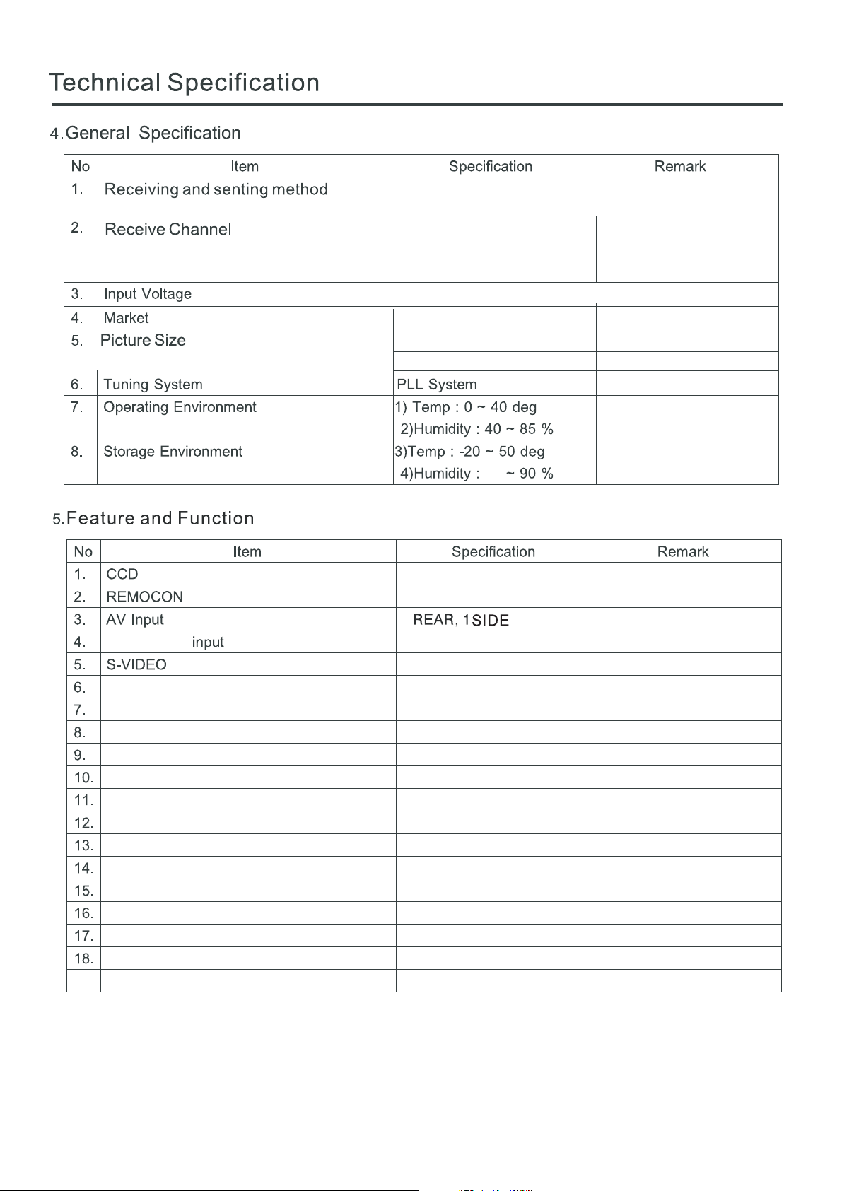
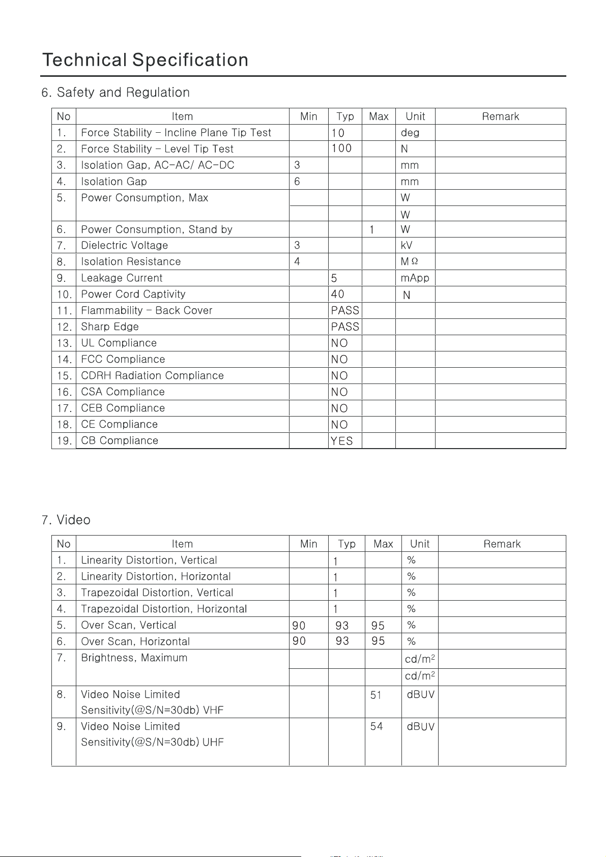
LCD 8M35S chassis.
-3-
Page 4
NTSC-M PAL-M PAN-N
VHF LOW 2~G
VHF HIGH H~W+27
UHF W+28~79
100-240V~ 50/60Hz
Latam
521.2 X 293.2 (mm)
521.2 X 293.2 (mm)
YES
TOSHIBA CODE
1
Component
1 REAR
1 REAR
VGA Input(with Jack Audio in)
HDMI
1 REAR
2 REAR, 1 SIDE
Headphone output 1 SIDE
NICAM Stereo
2 Carrier Dual
NICAM Dual
SSC (Split Screen) Mode
V-CHIP
Film Mode
Noise Reduction
Progressive Scan
Motion Detection
Dolby Virtual
Swivel Speaker19.
NO
NO
NO
NO
YES
NO
YES
YES
NO
NO
NO
55.25 MHz ~ 157.25 MHz
163.25 MHz ~ 457.25 MHz
463.25 MHz ~ 861.25 MHz
For 24S20 24S16
For 24E60
-4-
Page 5
65
55
For (24S20 24S16)
For (24E60)
-5-
300
300
For (24S20 24S16)
For (24E60)
Page 6

1920
1080
-6-
5
5
8
5
Page 7

80
40
40
3
2
1
4.2
50
0.5
12000
40
3
-7-
Page 8

1080
1920
Standard
Standard
30
40
NO
YES
8
6
46
46
NO
uv
uv
English
ON
ON
-8-
Following the Customer request
Page 9

4
2
4
0 40 7 0
0 40 7 0
0 40
40 85
-20 50
30000
-9-
Page 10

Chassis Block Diagram
D
SPL
SPR
6
C
PANEL
B
A
2010-4-1
R
AMP-TDA7266
LVDS
INVERT POWER
8M35 Block Diagram
XULI
SIDE
L
HEADPHONE
5
AV 1
HDMI 3
4
HDMI 1 HDMI 2
SWITCH
SVIDEO
VGA
3
SCART
REAR
R
21
Rear AV AV OUT
VL
YPb Pr
PI5V330SQE
MST740 KU
PIF
U10
SAWFILTER
IF
MST740 KE
SIF
U9
FLASH
EEPROM
+5V FOR ALL
EN25F16
3 4 65
24C32
+5V FOR STB
+12V FOR ALL
POWER SUPPLY
ANTENNA
D
1 2
TUNER
C
Key Control
Remote
B
SW
110V-240V
A
-10-
Page 11

IC Block Diagram
Functional Block Diagram
Thermal
Shutdown
AS1117
1A Fixed and Adjustable Low
Dropout Linear Regulator(LDO)
INPUT
Out
+
-
OUTPUT
GND (Fixed Output)
ADJ (Adjustable Output)
-11-
Page 12

IC Block Diagram
-12-
Page 13

IC Block Diagram
-13-
Figure 2. BLOCK DIAGRAM
EN25F16
Page 14

IC Block Diagram
-14-
Page 15

IC Block Diagram
-15-
A
T
V
CC
PI5V330S
Low On-Resistance Wideband/Video
Quad 2-Channel Mux/DeMux
V
CC
V
OU
IN
PI5V330S
75
S1 R1 T1
20pF
HP4396
HP11667A
Digital
Input
nalog
Output
PI5V330S
t
ON
50%
90%
C
50%
90%
t
OFF
L
Bandwidth MHz
700
600
500
400
300
200
100
0
0
10
20 30 40 50
Load, pF
Page 16

IC Block Diagram
-16-
Page 17

Main PCB Top/Bottom Layer
-17-
Page 18

Main PCB Top/Bottom Layer
-18-
Page 19

-19-
Press MENU button, In BRIGHTTNESS, then press 3195 (arbitrauy Effective).
3. ADC Adjust Method:
1) YPbPR Source
Input 100% color bar pattern signal, select AUTOTUNE item, Press button to auto adjust the ADC value, when show “OK” finished.
2)VGA Source:
Input tessellated white - black signal, select AUTOTUNE item, press button to auto adjust the ADC value, when show “OK” finished.
Page 20

-20-
Functional Overview
Front Panel
Note: The graphics are for representation only.
4
CH
+
5
6
7
8
9
10
CH
VOL+
VOL
MENU
SOURCE
1.Power Switch
3.Speakers
5.Channel Down Button
7.Volume Down Button
9.Source Button
3
2.Power Indicator / Remote Sensor
4.Channel Up Button
6.Volume Up Button
8.Menu Button
10.Standby Button
12
-6-
Page 21

-21-
Functional Overvie w
Back Panel
Note: The graphics are for representation only.
HDMI
-AUDIO-LR
SIDE AV IN
VIDEO
VGA IN
4
VGA
AUDIO IN
5
YPBPR IN
Y
P
B
P
R
6
VIDEO
VIDEO
LEFT
LEFT
RIGHT
RIGHT
AV IN AV OUT
2
78
S-VIDEO
9
75 ANT
1. HDMI:Connect HDMI input signal from signal source such as DVD.
2. SIDE AV IN\AV IN: Connect audio and video input signal from signal source such as DVD.
3. EARPHONE
VGA IN: Connect a PC via a VGA cable.
4.
5 VGA AUDIO IN:
.
6. Y Pb Pr
7. AV OUT:
: Audio output, speakers will be muted when earphone plugged in.
Audio input for PC and audio input for HDMI when the signal is DVI timing.
(Component input): Connect YPbPr signal from signal source such as DVD.
S
hares the same audio input as AV2.
Connect audio and video output the signal.
8. ANTENNA IN: Connect a coaxial cable to receive signal from the antenna or cable.
9.S-VIDEO: Connect S-VIDEO,Use same AUDIO input as AV input.
1
2
3
Page 22

-22-
Functional Overview
STANDBY
1
3
4
6
8
10
12
SOURCE RETURN
S. M P.P
MTS
SLEEP
ZOOM
1. STANDBY button
Press to turn the TV on or off(standby).
MUTE
2. MUTE button
Press to mute or restore the TV sound.
2
3. NUMBER buttons
Press to enter a channel number .
4. SOURCE button
Press to display the signal source
selection menu.
5
5. RETURN button
Press this button to return to the
7
INFO
CH
previously viewed channel.
9
6. SLEEP button
Press to select a time period after
which the TV will turn itself off.
11
7. INFO button
Press to display status such as zoom ,
13
CC
signal source ,sound systerm and so on .
8. VOLUME UP/DOWN button
Press to adjust the volume.
9. CHANNEL UP/DOWN button
Press to select memorized TV channel.
10. MENU button
Press this button to enter the menu screens
for various optional adjustable settings.
12. SOUND button(S.M)
Press to select a different sound effect.
13. PICTURE button(P.P)
Press to select a different picture effect.
Page 23

-23-
Functional Overview
STANDBY
SOURCE RETURN
SLEEP
S.M P.P
MTS
14
15
ZOOM
14.MTS button
Press to select desired sound output( Mono,
MUTE
Stereo, Sap) depending on the broadcasting
channel.
15. ZOOM button
Press to change the screen format(could be
different based on different models).
16. CC button
Press to select CC1\CC2\CC3\CC4,TEXT1\
TEXT2\TEXT3\TEXT4,OFF.
INFO
CH
CC
16
Page 24

-24-
Connections
EXTERNAL SCHEMATIC AND INSTALLATION
Antenna / Cable Connection
There are two kinds of antenna in use.
VHF TV ANTENNA
UHF TV ANTENNA
U/V MIXER
TWO KINDS OF ANTENNA
COAXIAL ANTENNA
FLAT CABLE
No need to install adapter
(Note 1)
Need to install adapter
(Note 2)
To TV VHF/UHF
ANTENNA jack
VHF/UHF
(75 )
1. Connect the plug of the antenna cable or CATV cable to the cable (not provided
with this unit), then connect to the antenna input of this unit for best reception.
2. If the antenna cable in your home is other than the above two, or you have
problems in installing the antenna, please contact your dealer.
Notes:
1. Current outdoor antenna or cable TV usually use 75 OHM coaxial antenna cable.
For better reception suggest using this kind of antenna cable.
2. Flat cable or indoor antenna are old designed, the reception may not be good enough.
Page 25

-25-
Menu Operation
MENUS CONTROL
STALLATION
This section explains the menus of your TV. Each menu is outlined and detailed to help you get
the most from your TV.
The scheme and description are in TV mode as below, there will be a note if there is exception.
Picture Settings
Contrast
Adjusts the difference between the light and dark areas
of the picture. To get better picture value, Contrast
should be adjusted to the proper value.
Brightness
Adjusts the brightness of the picture, and usually is
adjusted together with Contrast.
Tint
Adjusts the Tint of the picture to get better quality.
It is NTSC mode.available only in
Color
Adjusts the richness of color.
This function is not available in PC mode.
Sharpness
Adjusts the sharpness of the picture.
This function is not available in PC mode.
Backlight
Adjusts the level of back light.
(could be different base on different model)
Color Temp.
Adjusts the color temperature of the picture, to select
the option: Normal, Warm, Cold.
Note: Cold is for a more blue palette of picture colors,
Warm is for a more red palette of picture colors, and
Normal is between the two.
Picture Mode
Adjusts the brightness, contrast,color and sharpness of
the picture simultaneously.
CONTRAST
BRIGHTNESS
TINT
COLOR
SHARPNESS
BACK LIGHT
COLOR TEMP.
PICTURE MODE
MOVE SELECT EXIT
PICTURE
NORMAL
PERSONAL
MENU
50
50
50
50
50
50
Sound Settings
Bass
Adjusts the lowest part of the sound.
Treble
Adjusts the highest part of the sound.
Balance
Adjusts how much audio (loudness) gets sent to the
left and right speakers.
Sound Mode
Select the audio mode as you desired.
The audio mode are Standard,News,Music, Personal.
AVC
Auto volume control, select ON to enable volume to
remain at a pre-determined level should there be a
sudden change in volume during commercial breaks
or channel surfing.
BASS
TREBLE
BALANCE
SOUND MODE
AVC
MOVE SELECT EXIT
SOUND
PERSONAL
ON
MENU
50
50
0
Page 26

-26 -
Menu Operation
MENUS CONTROL
LANGUAGE
H-POSITION
V-POSITION
DURATION
OSD HALFTONE
MOVE SELECT EXIT
SLEEP TIMER
SCALE
C.CAPTION
V-CHIP
NOISE REDUCTION
FACTORY RESET
OSD
FUNCTION
ENGLISH
MENU
OFF
FULL
OFF
OFF
OSD Settings
Language
Select you desired OSD language.
H-Position
Changes the horizontal position of the OSD.
V-Position
50
50
Changes the vertical position of the OSD.
30
50
Duration
Set the OSD display duration when no operation.
OSD Halftone
select different OSD background transparent by it .
Function Settings
Sleep Timer
Lets you set a time for the TV to standby itself.
Scale
Select your desired picture zoom effect. You can
select :FULL, 4:3.
MOVE SELECT EXIT
MENU
V-CHIP
Select V-CHIP button toadjust the parent control of TV.
The factory default password is "0000".
Noise Reduction
You can select OFF, LOW, MID, HIGH to set the noise
reduction level to get a better picture view.
Factory Reset
Press to reset all the setting same as the out of box
setting.
-13-
Page 27

-27 -
Menu Operation
Channel Settings
Note:These settings are only available in TV mode.
Auto Search
Searches and saves channels automatically.
Notes:
1. If you press the MENU button to stop auto scan
process, the frist saved channel will be shown.
2.The TV is mute when starting auto scan.
3.You need set the correct sound system according
your local signal to get good performance before
or after auto scan.
AFT
Select ON to enable the frequenly auto tuning to
obtain the best reception.
Fine tuning
Tune RF frequency finely. Note can be selected when AFT is set as OFF. Press or button fine
tuning until the best reception is obtained.
AUTO SEARCH
AFT
FINE TUNING
ADD/ERASE
SOURCE
MTS
CHANNEL
MOVE SELECT EXIT
ON
ERASE
CATV
STEREO
MENU
ADD/ERASE
Set the current channel to skip or not.
Note: If the channel is set to be "ERASE", you can not select this channel by pressing Channel
UP/DOWN buttons on the remote control, you can select it exactly by entering the channel No by the
number buttons on the remote control.
SOURCE
Select the SOURCE of signals: AIR or CATV.
MTS
Adjusts the MTS of signals: MONO or STEREO.
Page 28

-28 -
Menu Operation
H-POSITION
V-POSITION
CLOCK
PHASE
AUTO ADJUST
GEOMETRY
MOVE SELECT EXIT
GEOMETRY SETTINGS
A in PC mode.vailable only
H-Position
Changes the horizontal position of the PICTURE.
V-Position
Changes the vertical position of the PICTURE.
50
50
Clock
30
Adjusts the sampling frequency of A/D.
50
Note: The option is usually adjusted with H-Position and
V-Position, This can make picture get better quality. You
also can use Auto function to make picture better.
MENU
Phase
Adjusts the sampling phase of A/D.
Note: You can adjust this value accordingly if there are
close bright dots on the picture or linear shimmer
phenomenon happens.
Auto Adjust
Adjusts the screen display to the best state automatically.
Note: You can adjust this value accordingly if the picture
is not in the proper position. Then adjust the H-Position,
V-Position ,H-Size and Phase options to get better
quality.
Page 29

-29 -
Menu Operation
This section explains the s .hortcuts and convenient functions
PICTURE MODE(P.P) shortcut
1. Press the PICTURE button on the remote control to display the current picture
state.
2. Press the PICTURE button repeatedly to select different picture effect.
3. The on screen display will disappear in 3 seconds if you stop adjusting.
Note: You can select Normal, Bright, Personal or Soft.
SLEEP shortcut
1. Press the SLEEP button on the remote control to display the sleep time.
2. Press the SLEEP button repeatedly to select a time period after which the
TV will turn itself off.
3. The on-screen display will disappear in 3 seconds if you stop adjusting.
Note: You can select 0 (off), 15 , 30, 45, 60, 90, or 120 minutes. In the last
minute of the sleep time, the words "POWER OFF" will display on the screen.
You can press any button to cancel the setting at this time.
SOUND MODE(S.M) shortcut
1. Press the SOUND button on the remote control to display the current sound state.
2. Press the SOUND button repeatedly to select different sound effect.
3. The on-screen display will disappear in 3 seconds if you stop adjusting.
Note: You can select Standard,News,Music,Personal.
SOURCE shortcut
ZOOM shortcut
Press to change the screen format: FULL, 4:3.
INFO shortcut
Press this button to display the settings on the screen.
RETURN shortcut
Press this button to return to the previously viewed channel.
Page 30

-30 -
TROUBLESHOOTING
NO PICTURE, NO SOUND
1. Check if the fuse or circuit breaker is working.
2. Plug another electrical device into the outlet to
make sure it is working or turned on.
3. Power plug is bad contact with the outlet.
4. Check the signal source.
NO COLOR
1. Change the color system.
2. Adjust the saturation.
3. Try another channel. Black-white program may
be received.
REMOTE CONTROL DOES NOT WORK
1. Change the batteries.
2. Batteries are not installed correctly.
3. Main power is not connected.
NO PICTURE, NORMAL SOUND
1. Adjust the brightness and contrast.
2. Broadcasting failure may happen.
NORMAL PICTURE, NO SOUND
1. Press the volume up button to increase volume.
2. Volume is set to mute, press MUTE to restore
sound.
3. Change the sound system.
4. Broadcasting failure may happen.
SNOWY DOTS AND INTERFERENCE
If the antenna is located in the fringe area of a
television signal where the signal is weak, the
picture may be marred by dots. When the signal
is extremely weak, it may be necessary to install
a special antenna to improve the reception.
1. Adjust the position and orientation of the
indoor/outdoor antenna.
2. Check the connection of antenna.
3. Fine tune the channel.
4. Try another channel. Broadcasting failure may
happen.
IGNITION
Black spots or horizontal streaks appear, or the
picture flutters or drifts. This is usually caused by
interference from car ignition system, neon lamps,
electric drills, or other electrical appliance.
GHOST
Ghosts are caused by the television signal
following two paths. One is the direct path, the
other is reflected from tall buildings, hills, or other
objects. Changing the direction or position of the
antenna may improve the reception.
RADIO FREQUENCY INTERFERENCE
This interference produces moving ripples or
diagonal streaks, and in some case, loss of
contrast in the picture. Find out and remove the
radio interference source.
UNORDERLY RIPPLES ON THE PICTURE
It is usually caused by local interference, such as
cars, daylight lamps and hair driers. Adjust the
antenna to minimize the interference.
BLANK SCREEN IN PC MODE
Perhaps the TV can not recognize the resolution set
by the PC. Suggest to change to the best resolution
or other standard resolutions of Windows system.
Set refresh rate to be 60Hz.
-18-
Page 31

-31 -
6SHFL¿FDWLRQ
Working voltage:
Power Consumption
Audio Output
Dimension(WxHxD)
Net Weight
Environment:
Working temperature: 5 C~35 C
Working humidity: 20%~80%
Storage temperature: -15 C~45 C
Storage humidity: 10%~90%
Channel coverage: 181 Full-Channel Cable TV
System:
TV: NTSC-M, PAL-M/N
AV: PAL, NTSC
Preset programs: 181
Status displaying method: On screen display
Function adjustment indicator: Menu display
oo
oo
AC 100-240V~50/60Hz
55W
5W+5W
579.5x148x421mm
5Kg
Language of OSD: Multiple options
RF aerial input: 75 ohm unbalanced
AV video input: 75 ohm, 1.0Vp-p, RCA
AV audio input: 10k ohm, 0.5Vrms
Page 32

of
18Tuesday, December 15, 2009
18Tuesday, December 15, 2009
14mA
C15
0.1uF
C15
0.1uF
C32
0.1uF
C32
VDDP
AVDDA
L4
380mA
310mA
NC/FBL4NC/FB
0.1uF
C31
0.1uF
C31
0.1uF
C30
0.1uF
C30
0.1uF
C29
0.1uF
C29
0.1uF
C28
0.1uF
C28
0.1uF
C27
0.1uF
C27
0.1uF
C26
0.1uF
C26
0.1uF
C25
0.1uF
C25
0.1uF
C24
0.1uF
C24
0.1uF
C23
2.2uF
C23
2.2uF
310mA
⊼ᛣ䗝⫼⺕⦴乱ᅮ⬉⌕
C38
0.1uF
C38
0.1uF
C37
0.1uF
C37
0.1uF
C36
0.1uF
C36
0.1uF
C33
2.2uF
C33
2.2uF
M3M3
M2M2
M1M1
678
9
1
234
5
1
C5
+5V
L115uH/3AL115uH/3A
3
SW
VCC
U1
EC9483U1EC9483
2
2
+12V
0.1uFC50.1uF
+
+
CA2
470uF/16V
CA2
SR34
SR34
0.1UF/NCC10.1UF/NC
C2
1
BS
CA1
CA1
6.2KR56.2K
COM6NC
C3
32
R8
4.7KR84.7K
+
+
0.1uFC20.1uF
C4 10nF/NCC4 10nF/NC
0.1UF/NCC30.1UF/NC
Q2
MMBT3904Q2MMBT3904
1
100uF/16V
100uF/16V
470uF/16V
R102KR102K
5
FB
GND
4
7.5K/NCR97.5K/NC
R9
DC/DC_SW
For PM Mode==>
VDDP_PM & AVDD_MPLL must be alive
1.4mA
C7
0.1uFC70.1uF
VDDP_PM
+3.3_STB
AVDD_MPLL
0.92*(1+Rup/Rdown)=5V---Rup=33K, Rdown=7.5K
R5
D01
D01
C1
EN
7
8
R4 33KR4 33KR6
C11
100pF
C11
100pF
6.8mA
C10
0.1uF
C10
0.1uF
C9
2.2uFC92.2uF
L2FBL2
FB
SOT-223
䌈⠛
,
ᇕ㺙
142mA
AVDD_VIF
L3FBL3
FB
+3.3V_normal
4
C22
C22
C21
C21
C20
C20
+
+
CA4
CA4
142mA
OUT
OUT
ADJ
ADJ
U2
U2
0.1uF
0.1uF
0.1uF
0.1uF
100pF
100pF
100uF/16V
100uF/16V
⊼ᛣ䗝⫼⺕⦴乱ᅮ⬉⌕
+3.3V_normal
3
IN
IN
1
AMS1117-3.3
AMS1117-3.3
+5V
C14
0.1uF
C14
0.1uF
CA3
CA3
100uF/16V
100uF/16V
C13
0.1uF
C13
0.1uF
C12
2.2uF
C12
2.2uF
TO-252
3
+12V_normal
AVDD_AU
VDDP_PM & AVDD_MPLL & AVDDA &
VDDP & VDDC must be alive
For Standby Mode==>
+3.3V_normal
+3.3_STB
VDDC
VCC1.26V
18Tuesday, December 15, 2009
1
<System power> v1.0
<MST740 FOR SKYWORTH>
<System power> v1.0
<MST740 FOR SKYWORTH>
<System power> v1.0
<MST740 FOR SKYWORTH>
C
C
C
Title
Size Document Number Rev
Date: Sheet of
Title
Size Document Number Rev
Date: Sheet of
Title
Size Document Number Rev
Date: Sheet
2
3
S2
HOLE-V8S2HOLE-V8
5V
U18
U18
p23051
p23051
power_on/off
power_on/off
R1
10KR110K
+5V_stb
4
+5V_stb
5
BL_ON/OFF
BL_ADJUST
12345678910111213
CN1CN1
Q1
MMBT3904Q1MMBT3904
32
1
4.7KR64.7K
R2
NC/0R2NC/0
R3
10KR310K
Q3
MMBT3904Q3MMBT3904
32
1
R7
10KR710K
WAKEUP
WAKEUP
Power on =1
PM==> Power down(PM Mode)=0
+12V
+12V
GND
POWER_ON/OFF
+5V_stb
5Vstb
14
+5V_future
GND
GND
GND
+5V_future
R210 0R / NCR210 0R / NC
DC/DC_SW
U17
U17
1
2 3
C149
0.1UF
C149
0.1UF
R221
R221
R224
10K
R224
10K
C148
0.1uF
C148
0.1uF
+12V
p23051
p23051
1
2 3
C146
0.1UF
C146
0.1UF
R216
10K
R216
10K
R219
10K
R219
10K
C145
0.1uF
C145
0.1uF
+5V_future +5V
Q23
Q23
10K
10K
32
1
MMBT3904
MMBT3904
R222 10KR222 10K
32
1
R217 10KR217 10K
power_on/off
power_on/off
Q21
Q21
MMBT3904
MMBT3904
+5V_stb
L7
NC/FBL7NC/FB
+5V_future
+5V
L14
NC/FB
L14
NC/FB
+5V_future
+5V
C6
0.1uFC60.1uF
BL_ADJUST
BL_ON/OFF
C8
2.2uFC82.2uF
R16
NC/10K
R16
NC/10K
R14 1KR14 1K
Q5
Q4
1
MMBT3904Q4MMBT3904
R13 4.7KR13 4.7K
ON_PBACK
ON_PBACK2
2 3
1
R15 4.7KR15 4.7K
PWM0
MMBT3904Q5MMBT3904
2 3
ADJ_PWM
R12
220
R12
220
R11
10K
R11
10K
ህ䳔䗝ᢽᇕ㺙
LDO
བᵰⳈ䕧ܹ
4
4
U3
U3
AMS1117-3.3
AMS1117-3.3
OUT
OUT
ADJ
ADJ
IN
IN
1.25V
TV 380mA
VCC1.26V
U4
U4
AMS1117-ADJ
AMS1117-ADJ
3
IN
IN
2
OUT
OUT
1
ADJ
ADJ
R17NCR17
NC
R19
3.0/2W
R19
3.0/2W
R18
3.0/2W
R18
3.0/2W
+5V
8mA
+3.3_STB
3
2
1
+5V_stb
678
+
CA6
470uF/16V+CA6
470uF/16V
C35
0.1uF
C35
0.1uF
R200RR20
0R
C34
0.1uF
C34
0.1uF
+
CA5
100uF/16V+CA5
100uF/16V
C19
0.1uF
C19
0.1uF
C18
2.2uF
C18
2.2uF
C17
0.1uF
C17
0.1uF
C16
2.2uF
C16
2.2uF
9
1
234
5
9
1
5
9
1
5
S1
HOLE-V8S1HOLE-V8
678
234
S4
HOLE-V8S4HOLE-V8
4
678
234
S3
HOLE-V8S3HOLE-V8
5
D D
C C
B B
A A
Page 33

of
2 8Tuesday, December 15, 2009
2 8Tuesday, December 15, 2009
2 8Tuesday, December 15, 2009
1
2
3
4
+3.3V_normal
Key&IR Pad
R131 220R131 220
R1301MR130
1M
CL=20pf of XTAL
X1
3
C88
C88
C87
C87
14.318MHZX114.318MHZ
27pF
27pF
27pF
27pF
R300 0RR300 0R
321
+5V_STB
+3.3_STB
+5V_stb
AVDD_VIF
VDDC VDDP
AVDDA
R132
R132
CN6
CN6
101112
LED_I/O
R136
100K
R136
100K
R135
100K
R135
100K
R134
4.7K
R134
4.7K
AVDD_AU
AVDD_MPLL
VDDP_PM
HWRESET
R138
R138
SYS_RST
CA12
100uF/16V+CA12
100uF/16V
+
3 2
1
Q13
Q13
D39 BAV99D39 BAV99
R137 4.7KR137 4.7K
100K
100K
GND
IR-in
HWRESET
100
100
MMBT3906
MMBT3906
CON12_2.0
CON12_2.0
123456789
+5V_stb
GND
GND
C94
100pF
C94
100pF
C93
100pF
C93
100pF
KEY1-in
KEY0-in
C92
100pF
C92
100pF
RXO2-
RXOC+
RXO0+
RXO0-
RXO1+
RXO1-
RXO2+
RXOC-
RXO1+
RXO2+
RXO2-
RXOC-
RXOC+
RXO0+
RXO0-
RXO1-
8642
8642
8642
8642
7531
7531
7531
7531
RP2
RP22X4
RP2
RP22X4
RP1
RP22X4
RP1
RP22X4
118
120
122
115
116
117
119
121
RLV2P/LVA2P
RLV1P/LVA1P
RLV0P/LVA0P
RLV2N/LVA2N
RLV1N/LVA1N
RLV0N/LVA0N
RLV3P/LVACLKP
RLV3N/LVACLKN
AVDD_AU
41
AVDD_VIF
39
AVDD_VIF
30
AVDD_VIF
31
AVDD_MPLL
26
AVDDP_1
69
AVDDP_1
74
AVDDP_1
80
AVDDP_1
110
AVDDP_1
124
AVDDP_1
146
VDDP_2
132
VDDC
67
VDDC
148
AVDD_ADC
153
AVDD_ADC
18
AVDD_ADC
10
XTAL_XOUT
27
XTAL_XIN
28
HWRESET
135
DDCD_SCL
RXA0P
RXACKP
DDCD_SDA
CEC
RXA0N
RXACKN
133
152
150
134
136
154
151
149
TXCLK-
G_TX1-
B_TX0-
B_TX0+
TXCLK+
SDA_HD
SCL_HD
C90
1nF
C90
1nF
R140
33K
R140
33K
C91
2.2uF
C91
2.2uF
RXO3+
RXO3-
RXO3+
RXO3-
RP3
RP22X4
RP3
RP22X4
114
113
RLV4P/LVA3P
RLV4N/LVA3N
RXA1P
156
155
G_TX1+
HPLUG
RXO4+
RXO4-
RXO4+
RXO4-
8642
8642
7531
7531
112
111
RLV5P/LVA4P
RLV5N/LVA4N
RXA2N
1
R_TX2-
R_TX2+
RXE0-
RXE0+
RXE1-
RXE0+
RXE0-
RP4
RP22X4
RP4
RP22X4
109
107
108
RLV6P/LVB0P
RLV6N/LVB0N
BIN1P4HOTPLUG
PB+
SOY
B_TX0-
TXCLK-
TXCLK+
TXCLK+
TXCLK-
123
CN16
CN16
PANEL
INTERFACE
RXE1+
RXE2+
RXE2-
RXE1-
RXE1+
RXE2-
RXE2+
8642
8642
7531
7531
RP5
RP22X4
RP5
RP22X4
105
104
106
RLV8P/LVB2P
RLV7P/LVB1P
RLV8N/LVB2N
RLV7N/LVB1N
RIN1P
GIN1P
SOGIN15RXA2P2RXA1N
GIN1M
8
6
7
PR+
Y+
C95 47nFC95 47nF
R139 47R139 47
B_TX0+
G_TX1-
G_TX1+
B_TX0-
G_TX1+
G_TX1-
B_TX0+
KEY0-in
RXEC-
RXEC-
103
LVBCLKP
VSYNC1
9
SC_FB
R_TX2-
R_TX2-
KEY1-in
RXEC+
8642
8642
7531
7531
R_TX2+
RXEC+
102
LVBCLKN
R_TX2+
4
RXE3-
RXE3-
RP6
RP6
101
LVB3P
SDA_HD
SDA_HD
RXE3+
RP22X4
RP22X4
100
11
HS_RGB
SCL_HD
CON4-2.0MM
CON4-2.0MM
RXE3+
RXE4-
99
LVB3N
HSYNC0
SCL_HD
Debug Port
Debug Port
RXE4-
RXE4+
RXE4+
8642
8642
7531
7531
98
LVB4P
LVB4N
BIN0P
12
BIN+
HPLUG
HPLUG
INPUT
DVI/HDMI
AMP_MUTE
ON_PBACK
panel_i/o
PWM3
WAKEUP
ON_PANEL
ON_PANEL
10K/NC
10K/NC
NC/10K
NC/10K
10K
10K
10K
10K
R162 100R162 100
10K
10K
RDZ
AD[0]
ON-PANEL
PWM3
AMP-MUTE
HD_SW
AU_SW
R167
R167
R166
R166
R165
R165
C114
0.1uF
C114
0.1uF
+5V +5V
I2C address
at A0.
0.1uF
0.1uF
8
VDD
U12
U12
CE#1SO2WP#3VSS
MX25LV040
MX25LV040
CZ
R161
NC/10K
R161
NC/10K
R1641KR164
+3.3V_normal
R1631KR163
Selection
+3.3V_normal
WAKEUP
4.7K
4.7K
4.7K
4.7K
4.7K
4.7K
7
HOLD#
SO
1K
1K
panel_i/opanel-i/o
ON_PBACK
R168100R168100
R171100R171100
WRZ
ALE
ON-PBACK
8
VCC
A01A12A23GND
U13
U13
SCK
6
SCK
R169 33KR169 33K
PWM2
LED_I/O
Q18
MMBT3904
Q18
MMBT3904
32
1
R26 10KR26 10K
Q14
MMBT3904
Q14
MMBT3904
32
1
I2C_SW
R172 4.7kR172 4.7k
R189 100R189 100
I2C-SW
LED_R
I2C_SCL
I2C_SDA
WP_EE
R170 100R170 100
5
6
7
WP
SCL
SDA
24C32
24C32
4
SIPWM1PWM1
5
SI
C129
NC/22pF
C129
NC/22pF
4
CZ
SCK
SI
SO
C115
0.1uF
C115
0.1uF
RP7
RP22X4
RP7
RP22X4
7531
7531
8642
8642
SPI_CK
SPI_CZ
SPI_DI
SPI_DO1
NC
R174NCR174
ADJ_PWM
NC
R173NCR173
PWM0
R25
220
R25
220
123
4
CN13
CN13
Debug Port
Debug Port
CON4-2.0MM
61
TCON057TCON158TCON259TCON360TCON4
TCON562TCON663TCON764TCON865TCON9
66
72
TCON1070TCON1171TCON12
Debug port
UART0
73
145
144
143
142
141
140
TCON13
TCON14
TCON15
TCON16
TCON17
TCON18
+5V
139
138
TCON19
TCON20
TCON21
TXD
RXD
R148
10K
R148
10K
R147
10K
R147
10K
INT 5v tolerance
SAR[0:2] 3.3v tolerance
IR-in
KEY1-in
KEY0-in
WAKEUP
SC_FS
AU_SW
R150 100R150 100
R146 1KR146 1K
R145 1KR145 1K
WakeUP 5v tolerance
128
131
130
129
127
137
INT
IRIN
SAR0
SAR1
SAR2
WAKEUP
CON4-2.0MM
TXD
RXD
TXD
RXD
DDCA_DA&DDCA_CLK 5v tolerance
R151100R151100
R152 100R152 100
126
125
GPIOD[5] 3.3v tolerance
GPIOD[4] 5v tolerance
DDCA_CLK
DDCA_DAT
LED_R
panel-i/o
GPIOD4
93
MUTE/GPIOD5
92
SPI_SCK
91
SPI_SCZ
90
SPI_SDI
89
SPI_SDO
88
AD[0]/GPIO/SPI_SIO2
87
AD[1]/GPIO/SPI_SIO3
86
AD[2]/GPIO
85
AD[3]/AUMCKO/GPIO
84
WRZ/AUWS/GPIO
83
RDZ/AUSCK/GPIO
82
ALE/AUSD0/GPIO
81
GPIOD0/TXD0
97
GPIOD1/RXD0
WRZ&RDZ 3.3v tolerance
96
GPIOD2/RXD1
95
GPIOD3/TXD1
94
SPI_DI
SPI_DO1
SPI_CK
SPI_CZ
ALE 5v tolerance
I2C_SCL
I2C_SDA
HD_SW
AD[0:1]3.3v tolerance
AD[2:3] 3.3v tolerance
WP_EE
I2C_SCL
I2C_SDA
AMP-MUTE
ON-PBACK
HD_SW
R153 100R153 100
R154 100R154 100
I2C-SW
ON-PANEL
GPIOD[0:3] 3.3v tolerance
R175
220
R175
220
+5V_stb
R160
10K
R160
10K
+3.3_STB
R187
10K
R187
10K
R159
10K
R159
10K
R191
NC/10K
R191
NC/10K
+3.3V_normal
R158
R158
R157
R157
R156
R156
R277
R277
R280
R280
+5V
GPIO Control Pins
U11U11
50
49
AUVRADP
AUVRADN
CVBSOut1
CVBSOUT1
AUVRP
AUVAG
51
AUVREF
INPUT
VIDEO
C112
C112
C111
C111
C110
C110
C109
C109
DAC_OUT_L
DAC_OUT_R
53
54
AUOutL2
AMP-L
AMP-R
0.1uF
0.1uF
10uF
10uF
0.1uF
0.1uF
10uF
10uF
HD/PC-Lin
AV1/SVIDEO-Lin
HD/PC-Rin
HD/PC-Lin
HD/PC-Rin
PWM0
PWM1
PWM2
PWM3
EPAD
GND
GND
GND
GND
AVSS
AVSS_VIF
AVSS_VIF
AVSS_MPLL
AVSS_ADC
AVSS_ADC
LINE_OUT_L55LINE_OUT_R
56
AUOutR2
AV2-Rin
AV1/SVIDEO-Rin
AV2-Lin
AV2-Lin
AV2-Rin
AV1/SVIDEO-Lin
AV1/SVIDEO-Rin
78
77
76
75
157
147
123
79
68
52
37
32
29
25
3
INPUT
AUDIO
MST740KU/E
LINE_IN_1R
LINE_IN_2L
SIFP
SOGIN0
GIN0M
GIN0P
15
13
14
GIN+
RIN+
SOG
C96 47nFC96 47nF
R141 47R141 47
VS_RGB
HS_RGB
HS_RGB
16
VS_RGB
17
VS_RGB
BIN+
BIN+
VSYNC0
SOG
VCOM0
CVBS3/C1
20
23
21
19
CVBS1
VCOM0
CVBSOut1
SV_C0
CVBS0
SV_Y0
C97 47nFC97 47nF
R142 47R142 47
Y+
PB+
PR+
GIN+
RIN+
SOY
SC_FB
SC_FS
GIN+
RIN+
PR+Y+SOY
PB+
SOG
SC_FB
INPUT
VGA
CVBS0/Y022CVBS2/Y1
RIN0P
33
SIFM
VIFM
VIFP
C9810uFC9810uF
Please close
WARNING !!!
CVBS0
AV1-Vin
SC_FS
INPUT
Y,Pb,Pr
SIFM35VIFM34CVBSOUT24CVBS1/C0
36
SIFP
C99 0.1uFC99 0.1uF
to chip.
+5V
LINE_IN_0L42TAGC
VR2738VIFP
43
40
C104 2.2uFC104 2.2uF
C100 2.2uFC100 2.2uF
C103 2.2uFC103 2.2uF
HD/PC-Lin
HD/PC-Rin
TAGC
R143
4.7K
R143
4.7K
LINE_IN_0R
LINE_IN_1L44LINE_IN_2R47AUVRM
45
46
C106 2.2uFC106 2.2uF
C107 2.2uFC107 2.2uF
C105 2.2uFC105 2.2uF
AV2-Lin
AV2-Rin
C108 0.1uFC108 0.1uF
AV1/SVIDEO-Rin
AV1/SVIDEO-Lin
C102
0.1uF
C102
0.1uF
R144 0RR144 0R
C101
0.1uF
C101
0.1uF
SV_C0
CVBS1
SV_Y0
AV2-Vin
SV-Yin
SV-Cin
48
AUCOM
AUOutL2
AUOutL2
AUOutR2
AUOutR2
ADJ_PWM
PWM0
PWM1
R155 10K/NCR155 10K/NC
PWM2
PWM3
PWM3
L10FBL10
FB
C113
C113
+3.3V_normal
+3.3V_normal
VIFP
VIFM
SIFM
SIFP
AMP-R
AMP-L
AMP-L
TAGC
TAGC
SIFM
VIFP
VIFM
SIFP
AMP-R
INPUT
OUTPUT
VIF
AUDIO
Mode
1
<MST739ku> V1.0
<MST740 FOR SKYWORTH>
<MST739ku> V1.0
<MST740 FOR SKYWORTH>
<MST739ku> V1.0
<MST740 FOR SKYWORTH>
D
D
D
Title
Size Document Number Rev
Date: Sheet
Title
Size Document Number Rev
Date: Sheet of
Title
Size Document Number Rev
Date: Sheet of
2
3
4
5
D D
C C
B B
A A
5
Page 34

V1.0
V1.0
V1.0
of
of
of
3 8Wednesday, September 16, 2009
3 8Wednesday, September 16, 2009
3 8Wednesday, September 16, 2009
1
2
AV_LOUT
R212
R212
C519
1nF
C519
1nF
C57
2.2uF
C57
2.2uF
D120NCD120
R50 47R50 47
R49
4.7K
R49
4.7K
+12V1
R51
R51
+
+
CA7
CA7
100uF/16V
100uF/16V
R481KR48
1K
+12V_normal
audio_OUT
1
<cvbs@Ypbpr interface>
<MST740 FOR SKYWORTH>>
<cvbs@Ypbpr interface>
<MST740 FOR SKYWORTH>>
<cvbs@Ypbpr interface>
<MST740 FOR SKYWORTH>>
A2
A2
AV_ROUT
R213
10K
R213
10K
10K
1 2
NC
R59
R5647R56
47
2 3
Q6
MMBT3904Q6MMBT3904
1
33K
33K
R55
10K
R55
10K
R53 10KR53 10K
C58 2.2uFC58 2.2uF
R54 100KR54 100K
C59 1nFC59 1nF
R52 1KR52 1K
R59
+12V1
10K
AV2-Rin 2
AV2-Rin
AV2-Lin
R325 0R325 0
R324 0R324 0
AV/YPBPR_R
AV/YPBPR_L
R32247K R32247K
R32347K R32347K
R30247K R30247K
R31647K R31647K
R29047K R29047K
R29147K R29147K
R30747K R30747K
R31147K R31147K
AV2-Lin 2
C320
C320
+5V
AV2-LinAV/YPBPR_L
3
8
16
X13Y
VCC
U28
U28
X012X114X215X311Y01Y15Y22Y34A10B
C328 2.2uF/NCC328 2.2uF/NC
C324 2.2uF/NCC324 2.2uF/NC
C336 2.2uF/NCC336 2.2uF/NC
SC_LINPUT AV2-Rin
AV/YPBPR_R
6
GND
0.1uF
0.1uF
7
INH
VEE
C337 2.2uF/NCC337 2.2uF/NC
SC_RINPUT
74HC4052/NC
74HC4052/NC
9
X1,Y1
X2,Y2
0
0 X0,Y0
0
1
01
AU-SW1 AU-SW0 Output
AU_SW2
C520
1nF
C520
1nF
1 2
C62
2.2uF
C62
2.2uF
D121NCD121
NC
R60 47R60 47
4.7K
4.7K
R61
R61
R7047R70
47
2 3
Q9
MMBT3904Q9MMBT3904
1
R69
10K
R69
33K
33K
10K
R67 10KR67 10K
C63 2.2uFC63 2.2uF
R68100KR68100K
C64 1nFC64 1nF
R66 1KR66 1K
VIDEO_OUT
+5V
Q7
MMBT3906Q7MMBT3906
R58
220
R58
220
Q8
MMBT3904Q8MMBT3904
1
R57
33k
R57
33k
C61
C61
0.1uF
0.1uF
C60
2.2uF
C60
2.2uF
CA8
CA8
+
+
100uF/16V
100uF/16V
L5 FBL5 FB
CVBSOut1
AV_VOUT
R63 75R63 75
R62 220R62 220
2 3
R64
R64
1 2
NC
D14NCD14
R6575R65
75
22k
22k
R2840R2840
HD_Y
SOY 2
C39 1nFC39 1nF
R21 47R21 47
U20
U20
R2850R2850
R2860R2860
HD_Pr
HD_Pb
PR+ 2
PB+ 2
Y+ 2
C40 47nFC40 47nF
C41 47nFC41 47nF
R23 47R23 47
R24 47R24 47 C42 47nFC42 47nF
R22 47R22 47
+5V
C162
C162
12
7
16
DA4DB
DC9DD
VCC
S1A2S1B5S1C11S1D14S2A3S2B6S2C10S2D13IN
HD1_Y
HD1_Pr
HD1_Pb
HD2_Y
HD2_Pb
HD2_Pr
8
0.1uF
0.1uF
15
GND
1
HD_SW
EN
NC/PI5V330
NC/PI5V330
HD_SW
+5V
A2
Title
Size Document Number Rev
Title
Size Document Number Rev
Title
Size Document Number Rev
X3,Y3
11
Date: Sheet
Date: Sheet
Date: Sheet
2
Near MST.IC
AUOutL2
Ground in the middle of the L/R
AUOutR2
3
AV1-Vin 2
AV1-Vin+
C47 47nFC47 47nF
R34 47R34 47
R3675R36
C49
C49
D7NCD7
AV1-VIDEO
4
AV Input
VIDEO INTERFACE
SV-Cin 2
SV1-Cin
C45 47nFC45 47nF
R3375R33
75
R32 47R32 47
C46
C46
NC/330pF
NC/330pF
75
NC
NC/330pF
NC/330pF
1 2
SV-Yin 2
SV1-YinSV1-Y
C51 47nFC51 47nF
R38 47R38 47
R3975R39
C52
C52
AV1/SVIDEO-Rin2
AV1/SVIDEO-RinAV1/SVIDEO_AUDIO_R
R42
R42
C53
C53
R4110KR4110K
D10NCD10
75
NC/330pF
NC/330pF
12K
12K
560pF
560pF
3
HD2_Pb
HD2_Y
SC_G
C157
C157
NC/2.2uF
NC/2.2uF
SC_B
C158
C158
HD2_Pr
NC/2.2uF
NC/2.2uF
SC_R
C161
C161
R279
R279
R281
R281
R276
R276
NC/2.2uF
NC/2.2uF
R313
R313
R314
R314
R312
R312
NC/47K
NC/47K
NC/47K
NC/47K
NC/47K
NC/47K
75R
75R
75R
75R
75R
75R
D68NCD68
NC
1 2
D67NCD67
NC
1 2
D66NCD66
NC
1 2
4
HD1_Pb
HD1_Pr
AV1/SVIDEO-Lin2
AV1/SVIDEO-Lin
R45 10KR45 10K
NC
1 2
AV1/SVIDEO_AUDIO_L
AV2-Vin 2
C48 47nFC48 47nF
R35 47R35 47
R47
12K
R47
12K
C56
560pF
C56
560pF
D13NCD13
NC
1 2
AV2_V AV2-Vin+
AV/YPBPR_LAV2_L
R3775R37
75
C50
C50
NC/330pF
NC/330pF
D8NCD8
NC
R40 10KR40 10K
1 2
AV/YPBPR_R
R43
12K
R43
12K
C54
560pF
C54
560pF
D11NCD11
NC
R44 10KR44 10K
1 2
AV2_R
SC_LINPUTSC_LIN
R46
12K
R46
12K
C55
560pF
C55
560pF
D12NCD12
NC
R79 10KR79 10K
1 2
SC_RINPUT
R270
12K
R270
12K
R287
R287
C159
C163
C163
D65NCD65
C159
560pF
560pF
NC
R27110KR27110K
1 2
SC_RIN
+5V
12K
12K
560pF
560pF
D72NCD72
NC
1 2
SC_FB
SC_FS 2
SC_FB
SC_FS
R29675R296
75
R297
R297
HD1_Y
R275
NC/47K
R275
R292
NC/47K
R292
C168
C168
0R/2.2uF
0R/2.2uF
HD_Pr
C169
C169
R295
R295
R293
R293
0R/2.2uF
0R/2.2uF
R305
R305
R306
R306
R304
R304
D69NCD69
D70NCD70
NC/47K
NC/47K
NC/47K
NC/47K
NC/47K
75R
75R
75R
75R
75R
75R
NC
NC
D71NCD71
NC
R268
NC/47K
R268
NC/47K
R315
NC/47K
R315
NC/47K
R310
NC/47K
R310
NC/47K
C167
0R/2.2uF
C167
0R/2.2uF
HD_Pb
HD_Y
1.5K
1.5K
NC/47K
R283
NC/47K
R283
NC/47K
R282
NC/47K
R282
NC/47K
+5V
C261
NC/47pF
C261
NC/47pF
C262
NC/47pF
C262
NC/47pF
R30110KR30110K
CON19
CON19
AV2_V
20
NC/SCART
NC/SCART
AV_VOUT
R298 0R298 0
D126NCD126
SC_R
Blanking I/O
SC_G
NC
D127NCD127
Switch
SC_B
SC_LIN
NC
1 2
SC_RIN
AV_LOUT
24681012141618
AV_ROUT
13579111315171921
5
B B
A A
1 2
D9NCD9
D6NCD6
NC
5
1 2
SV1-C
CN4
CN4
NC
1 2
HD_Pr
HD_Pb
HD_Y
AV2_R
AV2_V
AV2_L
AV_LOUT
AV_VOUT
AV_ROUT
34
2 156
S-VIDEO
S-VIDEO
AV1-VIDEO
AV1/SVIDEO_AUDIO_L
AV1/SVIDEO_AUDIO_R
2
6
112
446
3
557
CN5ACN5A
3
7
D D
2211335544779
CN2 2AV+1PYCN2 2AV+1PY
AUDIO&VIDEO Input
11
17
9
6
18
6
1313151517
18
16
16
14
14
12
12
10
10
8
8
C C
11
Page 35

HPLUG
V1.0
V1.0
V1.0
HPLUG
R74
10K
R74
10K
I2C_SDA
VCC_HDMI_SW
I2C_SDA
R273 4.7KR273 4.7K
R274 4.7KR274 4.7K
R264 100R264 100
SDA_CTL
SDA_HD
SCL_HD
17
I2C_RST
HPD1
POW1
A24
B24
VCC
A23
B23
GND
A22
B22
POW2
A21
B21
SCL2
SDA2
HPD2
64
C160
2.2u
C160
2.2u
I2C_SCL
I2C_SCL
R265 100R265 100
HOTPLUG
SCL_CTL
16
15
14
13
12
11
10
9
8
7
6
5
4
3
2
1
PS331
PS331
VCC_HDMI_SW
R78
R78
HDMI2_5V
R711KR71
VCC_HDMI_SW
HPD1
POW1
IN2D2+
IN2D2VCC_HDMI_SW
IN2D1+
IN2D1GND
IN2D0+
IN2D0POW2
IN2CLK+
IN2CLKSCL2
SDA2
HPD2
1K/NC
1K/NC
1K
HPD_SINK
4
U31
U31
+5VSTB
+5V
R76 4.7KR76 4.7K
1
32
Q10
Q10
MMBT3904
MMBT3904
AMS1117-3.3
AMS1117-3.3
IN
IN
OUT
OUT
ADJ
ADJ
3.3V_HDMI
3
2
1
L17
L17
L16
L16
C154
C154
C81
C81
C156
C156
C153
C153
C155
C155
C116
C116
C138
C138
C152
C152
C83
C83
VCC_HDMI_SW
L15FBL15FB
0R/NC
0R/NC
0R/NC
0R/NC
Title
Title
Title
1
B_TX0+
B_TX0-
B_TX0-
B_TX0+
G_TX1+
G_TX1+
G_TX1-
VCC_HDMI_SW
IN3CLK+
IN3CLK-
IN3D1+
IN3D2+
IN3D1-
IN3D2-
IN3D0-
IN3D0+
IN3CLK+
IN3CLK-
IN3D1+
IN3D2+
IN3D1-
IN3D2-
IN3D0-
IN3D0+
HPD3
SCL3
SDA3
R242 10RR242 10R
R24810RR24810R
R23110R/NCR23110R/NC
R234 10R/NCR234 10R/NC
R24110R/NCR24110R/NC
R245 10R/NCR245 10R/NC
R249 10R/NCR249 10R/NC
R25110R/NCR25110R/NC
+5V
HDMI3_5V
D61
D61
BAT54C
BAT54C
R243
47K
R243
47K
47K
47K
R247
R247
C89
0.1uF
C89
5
8
6
7
WP
SCL
VCC
A01A12A23GND
4
SDA
R206
R206
R205
R205
0.1uF
100R
100R
100R
100R
24C02/NC
24C02/NC
2
U22
U22
R252 10R/NCR252 10R/NC
HDMI BYPASS OPTION
HPD_SINK
SCL_HD
SDA_HD
C71
0.1uF
C71
0.1uF
HPD3
SCL3
SDA3
R255 1KR255 1K
HDMI3_5V
19
3
HOT PLUG
20
HDMI
HDMI
HDMI3
20
R250 10R/NCR250 10R/NC
G_TX1+
G_TX1-
B_TX0-
B_TX0+
D56NCD56
NC
D62NCD62
NC
16
18
17
SDA
+5V POWER
DDC/CEC GND
R_TX2+
15
14
SCL
R267 10R/NCR267 10R/NC
R_TX2-
D64NC
D64NC
13
NC
232322
22
R253 10R/NCR253 10R/NC
TXCLK+
RX3_C-
12
CEC
CLK-
R254 10R/NCR254 10R/NC
TXCLK-
GND
11
RX3_C+
CLK SHIELD
R246 10RR246 10R
R-L16W08-2
R-L16W08-2
RX3_0+
RX3_0-
9
8
10
CLK+
DATA0-
DATA0 SHIELD
RX3_0-
RX3_1+
RX3_1-
RX3_0+
6
7
DATA0+
R240 10RR240 10R
RX3_1-
5
DAT1A-
DATA1 SHIELD
R244 10RR244 10R
R239 10RR239 10R
RX3_2+
RX3_2-
RX3_2-
RX3_1+
3
4
DATA2-
DATA1+
R237 10RR237 10R
RX3_C+
2
R23810RR23810R
D53NCD53
D54NCD54
D57NCD57
D59NCD59
D58NCD58
D55NCD55
D60NCD60
D63NCD63
RX3_C-
RX3_2+
1
DATA2+
DATA2 SHIELD
21
CN15
CN15
21
NC
NC
NC
NC
NC
NC
NC
NC
R_TX2+
G_TX1-
TXCLK+
R_TX2-
TXCLK-
TXCLK+
TXCLK-
R_TX2+
R_TX2-
R256NCR256
NC
33
SDA_CTL
34
SCL_CTL
35
GND
Y4
36
R_TX2+
Z4
37
R_TX2-
38
VCC_HDMI_SW
Y3
39
G_TX1+
Z3
40
G_TX1-
41
GND
Y2
42
B_TX0+
Z2
43
B_TX0-
44
HPD_SINK
Y1
45
TXCLK+
Z1
46
TXCLK-
47
SCL_HD
48
SDA_HD
U19
U19
SDA_HD
SCL_HD
POW2
POW1
SDA_HD
SCL_HD
R259 37KR259 37K
R261 37KR261 37K
R262 3.6KR262 3.6K
R263 3.6KR263 3.6K
HDMI1_5V
HDMI2_5V
GND
IN1D0-
IN1D1-
IN1D2-
IN1D0+
IN1D1+
IN1D2+
R257 4.7KR257 4.7K
32
SDA_CTL
SCL_CTL
I2C_ADDR
R266 500_1%R266 500_1%
31
30
REXT
POWDN
B1429A14
VCC_HDMI_SW
22
24
27
25
28
NC
B1223A12
B1326A13
GND
VCC
GND
HPD_SINK
SCL_SINK
SDA_SINK
POW_SINK49HPD350SDA351SCL352B3153A3154POW355B3256A3257GND58B3359A3360VCC61B3462A3463CEXT
HPD3
SDA3
SCL3
IN3CLK-
IN3CLK+
POW3
IN3D0-
IN3D0+
GND
IN3D1-
POW3
R258 3.6KR258 3.6K
R260 37KR260 37K
HDMI3_5V
SDA1
SCL1
IN1CLK-
IN1CLK+
18
19
21
B1120A11
VCC
SCL1
IN3D1+
VCC_HDMI_SW
IN3D2-
IN3D2+
SDA1
of
4 8Tuesday, December 15, 2009
4 8Tuesday, December 15, 2009
4 8Tuesday, December 15, 2009
1
<HDMI&VGA>
<HDMI&VGA>
<HDMI&VGA>
<MST740 FOR SKYWORTH>>
<MST740 FOR SKYWORTH>>
<MST740 FOR SKYWORTH>>
A3
A3
A3
Size Document Number Rev
Date: Sheet
Size Document Number Rev
Date: Sheet of
Size Document Number Rev
Date: Sheet of
0.1uF
0.1uF
0.1uF
0.1uF
0.1uF
0.1uF
0.1uF
0.1uF
0.1uF
0.1uF
0.1uF
0.1uF
0.1uF
0.1uF
0.1uF
0.1uF
0.1uF
0.1uF
+
+
+
2
CA82
22uF/16V+CA82
22uF/16V
CA83
CA83
22uF/16V
22uF/16V
3
IN2CLK+
IN2CLK-
IN2D1+
IN2D2+
IN2D1-
IN2D2-
IN2D0-
NC
NC
NC
NC
11
clk shield
GND
IN2D0+
R235 10RR235 10R
R-L16W08-2
R-L16W08-2
RX2_0+
7
R232 10RR232 10R
RX2_0-
9
DAT0-
DAT0+
R230 10RR230 10R
R236 10RR236 10R
R233 10RR233 10R
R10110RR10110R
R103 10RR103 10R
R194 10RR194 10R
D40NCD40
NC
D41NCD41
NC
D46NCD46
NC
D48NCD48
NC
D47NCD47
NC
D45NCD45
NC
D49NCD49
NC
D51NCD51
NC
RX2_1+
RX2_1-
RX2_2+
RX2_2-
RX2_C+
RX2_C-
3
6
10
1
4
12
clk-
clk+
DAT2-
DAT1-
DAT2+
DAT1+
HDMI
HDMI
4
5
IN1CLK+
IN1CLK-
IN1D1+
IN1D2+
IN1D1-
IN1D2-
IN1D0-
IN1D0+
HDMI1_5V
+5V
4
5
D15
D15
BAT54C
BAT54C
CN11
CN11
R73
R73
R72
R72
HDMI1_5V
22
GND20GND21GND
C65
C65
47K
47K
47K
47K
0.1uF
0.1uF
SDA1
SCL1
15
18
17
16
+5V
DDC SCL
CEC/DDC GND
HPD1
R272 1KR272 1K
D16
D16
19
13
HPD
CEC
DDC SDA
5
2
8
Dat1 shield
Dat2 shield
Dat0 shield
D19NC D19NC
D18NC D18NC
NC
NC
11
clk shield
GND
R-L16W08-2
R-L16W08-2
R80 10RR80 10R
RX1_0+
7
DAT0+
R84 10RR84 10R
R82 10RR82 10R
R86 10RR86 10R
R81 10RR81 10R
RX1_0-
R87 10RR87 10R
R85 10RR85 10R
R83 10RR83 10R
D27NCD27
NC
D26NCD26
NC
D25NCD25
NC
D35NCD35
NC
D24NCD24
NC
D23NCD23
NC
D21NCD21
NC
D20NCD20
NC
RX1_1+
RX1_1-
RX1_2+
RX1_2-
RX1_C+
RX1_C-
3
6
9
10
1
4
12
clk-
clk+
DAT2-
DAT1-
DAT0-
DAT2+
DAT1+
HDMI
HDMI
+5V
D17
D17
BAT54C
BAT54C
CN14
HDMI2
CN14
R75
R75
R77
R77
HDMI2_5V HDMI2_5V
22
GND20GND21GND
C70
C70
47K
47K
47K
47K
0.1uF
0.1uF
18
17
+5V
D50NCD50
D22NCD22
HPD2
SDA2
SCL2
R269 1KR269 1K
D52
D52
19
13
15
16
HPD
CEC
DDC SCL
DDC SDA
CEC/DDC GND
5
2
8
Dat1 shield
Dat2 shield
Dat0 shield
D D
C C
B B
A A
Page 36

VS_RGB
HS_RGB
1
HS_RGB
I2C_SW
I2C_SW
I2C_SDA
I2C_SCL
I2C_SW
of
of
of
5 8Wednesday, February 03, 2010
5 8Wednesday, February 03, 2010
5 8Wednesday, February 03, 2010
1
NC
R126NCR126
I2C_SCL
I2C_SDA
32
D
D
SG
SG
R104 NCR104 NC
VGA_RX
Q27 NC/2N7002
Q27 NC/2N7002
1
R108NCR108
NC
R188NCR188
1
32
Q25
Q25
NC/MMBT3904
NC/MMBT3904
R106NCR106
NC
NC
PC INPUT V1.0
<MST740 FOR SKYWORTH>>
PC INPUT V1.0
<MST740 FOR SKYWORTH>>
PC INPUT V1.0
<MST740 FOR SKYWORTH>>
A4
A4
A4
Title
Size Document Number Rev
Title
Size Document Number Rev
Title
Size Document Number Rev
+5V
2
Date: Sheet
Date: Sheet
Date: Sheet
3
32
NC/MMBT3904
NC/MMBT3904
NC
1
Q24
Q24
1
Q26
Q26
NC/2N7002
NC/2N7002
32
D
D
SG
SG
BIN+
GIN+
RIN+
C67 47nFC67 47nF
C66 47nFC66 47nF
2
C68 47nFC68 47nF
SOG
C69 1nFC69 1nF
R96 100R96 100
R95 100R95 100
D32NCD32
R99
R99
R98
R98
D31NCD31
NC
10K
10K
10K
10K
NC
close to MST IC
R105NCR105
+5V
RXD
RXD
R97 0RR97 0R
SCL
TXD
TXD
R100 0RR100 0R
SDA
D34NCD34
R107NCR107
NC
R88 47R88 47
R8947R8947
R91 47R91 47
R90 47R90 47
R9475R94
75
75
R9375R93
R9275R92
B
R
G
3
75
B-
G-
R-
D30NCD30
NC
NC
R102 NCR102 NC
VGA_TX
D33NCD33
D29NCD29
D28NCD28
4
NC
NC
VGA_RX
162738495
10
CN12
VGA
CN12
VGA
1617
11
12
13
14
15
NC
+5V_all
D44
BAT54C
D44
BAT54C
R214
R214
R226
R226
R345
R345
R344
R344
10K
10K
10K
10K
100R
100R
100R
100R
HD_5V
HD/PC-Lin2
HD/PC-Rin2
HD/PC-RinHD/PC_RIN
R31
12K
R31
12K
C44
560pF
C44
560pF
R30
12K
R30
12K
C43
560pF
C43
560pF
C124
0.1uF
C124
0.1uF
R29 10KR29 10K
R2810KR2810K
D5NCD5
D4NCD4
HD/PC_LIN HD/PC-Lin
NC
NC
4
1 2
1 2
5
8
7
6
5
VGA_TX
VCC
A01A12A23GND
U23
U23
WP
SCL
SDA
24C02/NC
24C02/NC
23541
7
6
5
4
CN3
PHONEJACK
CN3
PHONEJACK
D D
C C
B B
A A
Page 37

of
6 8Tuesday, February 02, 2010
6 8Tuesday, February 02, 2010
6 8Tuesday, February 02, 2010
1
VIFM
VIFP
R335
R335
R334
R334
6.8K/NC
6.8K/NC
6.8K/NC
6.8K/NC
U10
U10
VIFM
R124 0RR124 0R
5
K3953D
K3953D
1
OUT2
SAW
SAW
IN
C82
C82
VIF
D1
10nF
10nF
SIF_CTL
VIFP
R1250RR125
0R
R2890RR289
0R
4
OUT1
GND
3
ING
2
1
Q36
32
R336
6.8K/NC
R336
6.8K/NC
R333
6.8K/NC
R333
6.8K/NC
Q36
NC / MMBT3904
NC / MMBT3904
OR/BA892/BA982D1OR/BA892/BA982
SIFP
SIFM
SIF_CTL
SIF
SIFP
SIFM
R1210RR121
0R
R2090RR209
R1190RR119
0R
4
5
SIF
OUT1
OUT2
U8
U8
K9650M
K9650M
1
SAW
SAW
IN
GND
ING
2
D43
OR/BA892/BA982
D43
OR/BA892/BA982
2
use for two standard audio system.
this is for PAL BG/DK/I,SECAM L &
switch L'.
layout placement
Close to Mstar IC
R149
3.3K/NC
R149
3.3K/NC
R133
6.8K/NC
R133
6.8K/NC
5V-tuner
C77
10nF
C77
10nF
0R
3
1
Q35
Q35
NC / MMBT3904
NC / MMBT3904
32
R207
0R/NC
R207
0R/NC
R199
6.8K/NC
R199
6.8K/NC
5V-tuner
1
<MST740 FOR SKYWORTH>
<MST740 FOR SKYWORTH>
<MST740 FOR SKYWORTH>
<Tuner> V1.0
<Tuner> V1.0
<Tuner> V1.0
C
C
C
Title
Size Document Number Rev
Date: Sheet of
Title
Size Document Number Rev
Date: Sheet of
Title
Size Document Number Rev
Date: Sheet
2
3
R111
680
R111
680
L6
0.82uHL60.82uH
VIF_12V
R110
6.8K
R110
6.8K
C72
10nF
C72
10nF
+
+
Layout placement
Close to Tuner
CA30
CA30
100uF/16V
100uF/16V
R109
150
R109
150
+12V_normal VIF_12V
4
GND3
TDQ-6F6/T126CWU7TDQ-6F6/T126CW
U7
13
16
15
14
GND5
GND4
GND1
NC
12
NC
11
NC
10
AGC
9
AGC
NC
8
5VB
7
SCL
6
SDA
AS
NC
IF
BT
TUNER_SCL
5
TUNER_SDA
4
3
2
IF_TV
1
R112
R112
Tuner_+30V
5V-tuner
1.2K/nc
1.2K/nc
C73
C73
32
10nF/nc
10nF/nc
1
IF_TV
R1140RR114
0R
R116
20R
R116
20R
Q11
Q11
2SC2216/2SC2217
2SC2216/2SC2217
R1151KR115
1K
R11347R113
47
I2C_SCL
C74
10nF
C74
10nF
R117 1KR117 1K
Tuner_+30V 40V
C75
0.1uF
C75
0.1uF
+
+
CA9
CA9
100uF/16V
100uF/16V
I2C_SDA
I2C_SDA
I2C_SCL
R118
100K
R118
100K
D36
33V
D36
33V
R122 100R122 100
R120 100R120 100
C76
0.1uF
C76
0.1uF
TUNER_SDA
TUNER_SCL
TAGC
TAGC
R123
10K
R123
10K
D37
D37
1N4148
1N4148
C79
27pF
C79
27pF
C78
27pF
C78
27pF
C80
0.1uF
C80
0.1uF
AGC
+5V
L8 FB/NCL8 FB/NC
C86
2.2uf
C86
IN
IN
R127
R127
3
2
1
NC/22R/2W
NC/22R/2W
2.2uf
C84
0.1uF
C84
0.1uF
C85
NC/0.1uF
C85
NC/0.1uF
CA10
CA10
NC/100uF/16V
NC/100uF/16V
WARNING !!!
+
+
CA11
CA11
40V+12V_normal
2.2uF/50V
2.2uF/50V
D381N4148D381N4148
Q12
2SC1815
Q12
2SC1815
L9 100uHL9 100uH
R129 4.7KR129 4.7K
PWM3
R12810RR12810R
PWM3
5V-tuner
OUT
OUT
4
GND
GND
U9
U9
NC/LM7805
NC/LM7805
3
4
5
D D
C C
+12V_normal
B B
A A
5
Page 38

V1.0
V1.0
V1.0
CN8
CN9
CN9
1
2
CON2_2.54
CON2_2.54
1
20
GND19GND18GND17GND16GND15GND14GND13GND12GND
GND
-INV11SGND2SVRR3OUT14PGND5OUT26Vp7M/S8-INV2
U16
TDA1517P/NC
U16
TDA1517P/NC
11
AMP-Lout+
5
11
20
23
25
15
GND
9
10
R416
0/NC
R416
0/NC
20
25
NC1
NC3
2OUT+
GND2
17
U21
U21
1IN+
2IN+
4
12
15INCH TO 20INCH
AMP-Lout+
AMP-Rout+
C135
C135
470uF/16V/NC
100uF/16V
100uF/16V
+
+
C131
2
C131
+12VB
FB
L13FBL13
+12V_normal
3
470uF/16V/NC
+
+
+
+
C134
C134
470uF/16V/NC
470uF/16V/NC
R197
R197
R196
R196
20K/NC
20K/NC
20K/NC
20K/NC
C121 2.2ufC121 2.2uf
R229 10KR229 10K
C122 2.2ufC122 2.2uf
R22810KR22810K
Q34
Q34
C181
C181
R320
R320
1nF
1nF
NC/33K
NC/33K
SOT
SOT
B
B
132
R215 10KR215 10K
C182
1nF
C182
1nF
R327
NC/1.5K
R327
NC/1.5K
C
3904
3904
C127 100uF/16V+C127 100uF/16V
C
23
23
Q32
3904
Q32
3904
SOT
SOT
E
B
E
B
132
R318 10KR318 10K
C
C
23
23
Q17
3906
Q17
3906
SOT
SOT
E
B
E
B
132
+
R20810KR20810K
C
C
C
23
23
E
E
C
23
23
SOT
SOT
E
B
E
B
Q33
Q33
3904
3904
132
R339 10KR339 10K
C165
10uF/16V+C165
10uF/16V
+
R319
10K
R319
10K
1
2
AMP-Lout-
AMP-Rout+
14
10
18
1
18
23
2OUT-
1OUT+
AMUTE6VCC1
SGND9VCC2
Standby
22
7
21
22
R27
R27
Phone-MUTE
R314
R314
+
+
C164
C164
C151
C151
R317
0 R
R317
0 R
R3081KR308
1K
R330NCR330
NC
C128
C128
+
+
220uF/16V
220uF/16V
D77
1N4148
D77
1N4148
NC2
21
3
R303
R303
CN8
CON2_2.0
CON2_2.0
AMP-Rout-
19
19
100K
100K
+12VB
100K
100K
47uF/16V
47uF/16V
1uF
1uF
0 R
0 R
Q20
Q20
2
1OUT-
24
13
24
3904
3904
R332
R332
10K
10K
AMP_MUTE
R220
0/NC
R220
0/NC
R223
0/NC
R223
0/NC
TDA7266SA
TDA7266SA
TDA7266SA+TDA7266
TDA7266SA+TDA7266
GND1
16
PWGND
8
C184
0.1uF
C184
0.1uF
+
+
CA42
CA42
1000uF/16V
1000uF/16V
C
C
23
23
SOT
SOT
E
B
E
B
132
<MST740 FOR SKYWORTH>
<MST740 FOR SKYWORTH>
<MST740 FOR SKYWORTH>
Title
Size Document Number Rev
Title
Size Document Number Rev
Title
22INCH TO 32INCH
Size Document Number Rev
of
7 8Sunday, February 21, 2010
7 8Sunday, February 21, 2010
7 8Sunday, February 21, 2010
1
<Audio AMP>
<Audio AMP>
<Audio AMP>
A3
A3
A3
Date: Sheet
Date: Sheet of
Date: Sheet of
2
3
R3281KR3281K
R204 1KR204 1K
AMP-ROUT
AMP-LOUT
R192
33K
R192
33K
TL062
TL062
C143 100pFC143 100pF
R193 33KR193 33K
C125
1nF
C125
1nF
R288 10KR288 10K
C236 10nFC236 10nF
U14B
U14B
OP_VCC1
100uF/16V
100uF/16V
U14A
U14A
PH-Lin
1
84
-
+
-
+
3
2
R190 10KR190 10K
C123 2.2uFC123 2.2uF
AMP_L
+
+
CA15
CA15
R184
20R
R184
20R
+12V_normal
4
6VBuf1
C120
C120
0.1uF
0.1uF
OP_VCC1
R186 33KR186 33K
+
CA14100uF/16V+CA14100uF/16V
R185 33KR185 33K
PH-Rin
7
84
-
+
-
+
5
6
R195 10KR195 10K
C136 2.2uFC136 2.2uF
AMP_R
R198
33K
R198
33K
TL062
TL062
C140 100pFC140 100pF
R200 33KR200 33K
C137
1nF
C137
1nF
R299 10KR299 10K
C237 10nFC237 10nF
+5V
+12VB
CA17 100uF/16V+CA17 100uF/16V
PH-Lin
+
PH-Lout
R463 0/NCR463 0/NC
PH-Rout
AMP-ROUT
235
1
PH-RinPH-Rout
+
AMP-LOUT
4
R464 0/NCR464 0/NC
PH-Lout
AMP_MUTE2
AMP-MUTE=1,MUTE;AMP-MUTE=0,ON;
4
CA16 100uF/16V+CA16 100uF/16V
5
R278100R278100
AMP-L2
D D
C C
R294 100R294 100
AMP-R2
CN10
PHONEJACK
CN10
PHONEJACK
B B
A A
5
Page 39

of
of
of
88Wednesday, September 16, 2009
88Wednesday, September 16, 2009
88Wednesday, September 16, 2009
1
<MST740 FOR SKYWORTH>
<MST740 FOR SKYWORTH>
<MST740 FOR SKYWORTH>
Title
Title
Title
2
VCC-Panel
U15
U15
p23051
p23051
+
+
CA13
CA13
100uF/16V
100uF/16V
1
RXO0-
RXO0-
RXO0+
RXO1-
RXO0+
RXO1-
RXO1+
RXO2-
RXO1+
RXO2-
2 3
C117
0.1UF
C117
3
0.1UF
R177
10K
R177
10K
R176
10K
R176
10K
Q15
Q15
32
1
MMBT3904
MMBT3904
RXOC-
RXO2+
RXO2+
RXOC-
RXO3-
RXOC+
RXOC+
RXO3-
RXO4-
RXO3+
RXO3+
RXO4-
RXO4+
RXO4+
RXE1+
RXE1-
RXE0+
RXE0-
RXE2-
RXE0-
RXE0+
RXE1-
RXE1+
R182
R182
+3.3V_normal
RXE2+
RXE2-
RXE2+
NC/4.7K
NC/4.7K
RXEC-
RXEC-
RXEC+
RXE3-
RXEC+
RXE3-
R183
R183
RXE4-
RXE3+
RXE3+
RXE4-
RXE4+
RXE4+
NC/0
NC/0
Size Document Number Rev
Size Document Number Rev
Size Document Number Rev
1
<Panel interface> V1.0
<Panel interface> V1.0
<Panel interface> V1.0
B
B
B
Date: Sheet
Date: Sheet
Date: Sheet
2
3
R178
4.7K
R178
+3.3V_normal
4.7K
R179 4.7KR179 4.7K
32
Q16
Q16
1
R180 4.7KR180 4.7K
ON_PANEL
MMBT3904
MMBT3904
CN7
CN7
GND
GND
RXE1-
18
RA2-
RA2+
17
RXO4-
RXE0-
MODE
20
28
22
24
26
GND
GND
GND
RA1-
RA0-
RA1+
RA0+
GND
GND
GND
19
21
23
25
27
RXE3-
GND
RXE2-
RXE4-
RXEC-
10
12
6
5
8
GND
GND
7
GND
GND
9
RA4-
RA4+
11
14
RA3-
RA3+
13
16
RACK-
RACK+
15
2
4
VCC
VCC
VCC
VCC
1
3
RXO3-
30
RB4-
RB4+
29
RXOC-
32
RB3-
RB3+
31
RXO2-
RXO1-
34
36
RB2-
RBCK-
RBCK+
RB2+
33
35
RXO0-
RB1-
RB1+
GNDGND
38
40
RB0-
RB0+37GND
39
GND
CON40
CON40
C118
0.1uF
C118
0.1uF
L12FBL12FB
L11 NCL11 NC
VCC-Panel
GND
C119
0.1uF
C119
0.1uF
4
RXE4+
RXE3+
RXEC+
RXE2+
RXE1+
GND
RXE0+
GND
RXO4+
RXO3+
RXO2+
RXOC+
RXO1+
RXO0+
4
+5V
+12V_normal
5
ON_PANEL
+3.3V_normal
NC/4.7K
NC/4.7K
panel_i/o
panel_i/o
R181
R181
PANEL
INTERFACE
panel_i/o
5
D D
C C
B B
A A
 Loading...