

Hitachi 75176 Diagram
SN75176A
DIFFERENTIAL BUS TRANSCEIVER
SLLS100A – JUNE 1984 – REVISED MA Y 1995
D
Bidirectional Transceiver
D
Meets or Exceeds the Requirements of
ANSI Standards EIA/TIA-422-B and ITU
Recommendation V.1 1
D
Designed for Multipoint Transmission on
Long Bus Lines in Noisy Environments
D
3-State Driver and Receiver Outputs
D
Individual Driver and Receiver Enables
D
Wide Positive and Negative Input/Output
Bus Voltage Ranges
D
Driver Output Capability...±60 mA Max
D
Thermal-Shutdown Protection
D
Driver Positive- and Negative-Current
Limiting
D
Receiver Input Impedance...12 kΩ Min
D
Receiver Input Sensitivity...±200 mV
D
Receiver Input Hysteresis...50 mV Typ
D
Operates From Single 5-V Supply
D
Low Power Requirements
description
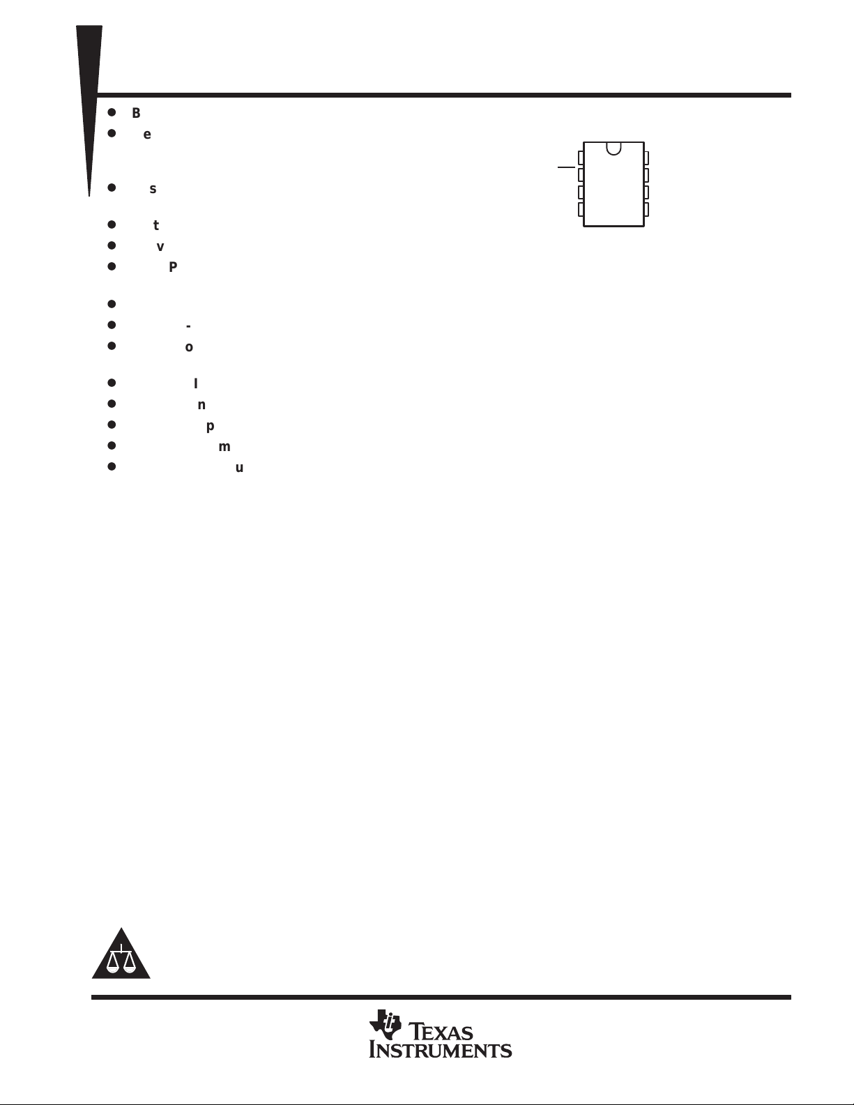
D OR P PACKAGE
(TOP VIEW)
R
RE
DE
1
2
3
D
4
8
7
6
5
V
CC
B
A
GND
The SN75176A differential bus transceiver is a monolithic integrated circuit designed for bidirectional data
communication on multipoint bus-transmission lines. It is designed for balanced transmission lines and meets
ANSI Standard EIA/TIA-422-B and ITU Recommendation V.11.
The SN75176A combines a 3-state differential line driver and a differential input line receiver, both of which
operate from a single 5-V power supply. The driver and receiver have active-high and active-low enables,
respectively , that can be externally connected together to function as a direction control. The driver differential
outputs and the receiver differential inputs are connected internally to form differential input /output (I/O) bus
ports that are designed to offer minimum loading to the bus whenever the driver is disabled or V
= 0. These
CC
ports feature wide positive and negative common-mode voltage ranges making the device suitable for party-line
applications.
The driver is designed to handle loads up to 60 mA of sink or source current. The driver features positive- and
negative-current limiting and thermal shutdown for protection from line fault conditions. Thermal shutdown is
designed to occur at a junction temperature of approximately 150°C. The receiver features a minimum input
impedance of 12 kΩ, an input sensitivity of ±200 mV, and a typical input hysteresis of 50 mV.
The SN75176A can be used in transmission-line applications employing the SN75172 and SN75174 quadruple
differential line drivers and SN75173 and SN75175 quadruple differential line receivers.
The SN75176A is characterized for operation from 0°C to 70°C.
Please be aware that an important notice concerning availability, standard warranty, and use in critical applications of
Texas Instruments semiconductor products and disclaimers thereto appears at the end of this data sheet.
PRODUCTION DATA information is current as of publication date.
Products conform to specifications per the terms of Texas Instruments
standard warranty. Production processing does not necessarily include
testing of all parameters.
POST OFFICE BOX 655303 • DALLAS, TEXAS 75265
Copyright 1995, Texas Instruments Incorporated
1
SN75176A
DIFFERENTIAL BUS TRANSCEIVER
SLLS100A – JUNE 1984 – REVISED MA Y 1995
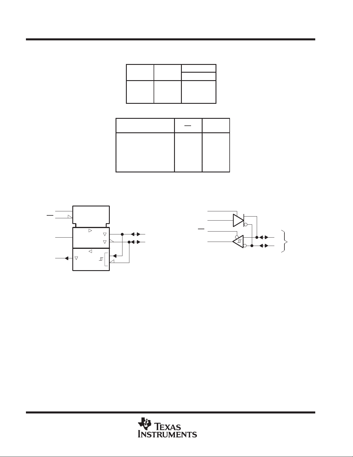
INPUT ENABLE
DIFFERENTIAL INPUTS
VID ≥ 0.2 V L H
–0.2 V < VID < 0.2 V L ?
VID ≤ – 0.2 V L L
H = high level, L = low level, ? = indeterminate,
X = irrelevant, Z = high impedance (off)
Function Tables
DRIVER
OUTPUTS
D DE
H H H L
L H L H
X L Z Z
RECEIVER
A – B RE R
X H Z
Open L ?
A B
ENABLE OUTPUT
logic symbol
DE
RE
†
This symbol is in accordance with ANSI/IEEE Std 91-1984
and IEC Publication 617-12.
†
3
EN1
2
EN2
4
D
1
R
2
1
1
logic diagram (positive logic)
3
DE
4
D
6
A
7
B
RE
2
6
1
R
A
7
Bus
B
2
POST OFFICE BOX 655303 • DALLAS, TEXAS 75265

PACKAGE
A
schematics of inputs and outputs
SN75176A
DIFFERENTIAL BUS TRANSCEIVER
SLLS100A – JUNE 1984 – REVISED MA Y 1995
EQUIVALENT OF EACH INPUT
V
CC
R
(eq)
Input
Driver input: R
Enable inputs: R
R
= equivalent resistor
(eq)
= 3 kΩ NOM
(eq)
= 8 kΩ NOM
(eq)
TYPICAL OF A AND B I/O PORTS
16.8 kΩ
NOM
Input/Output
Port
960 Ω
NOM
960 Ω
NOM
V
CC
GND
TYPICAL OF RECEIVER OUTPUT
V
CC
85 Ω
NOM
Output
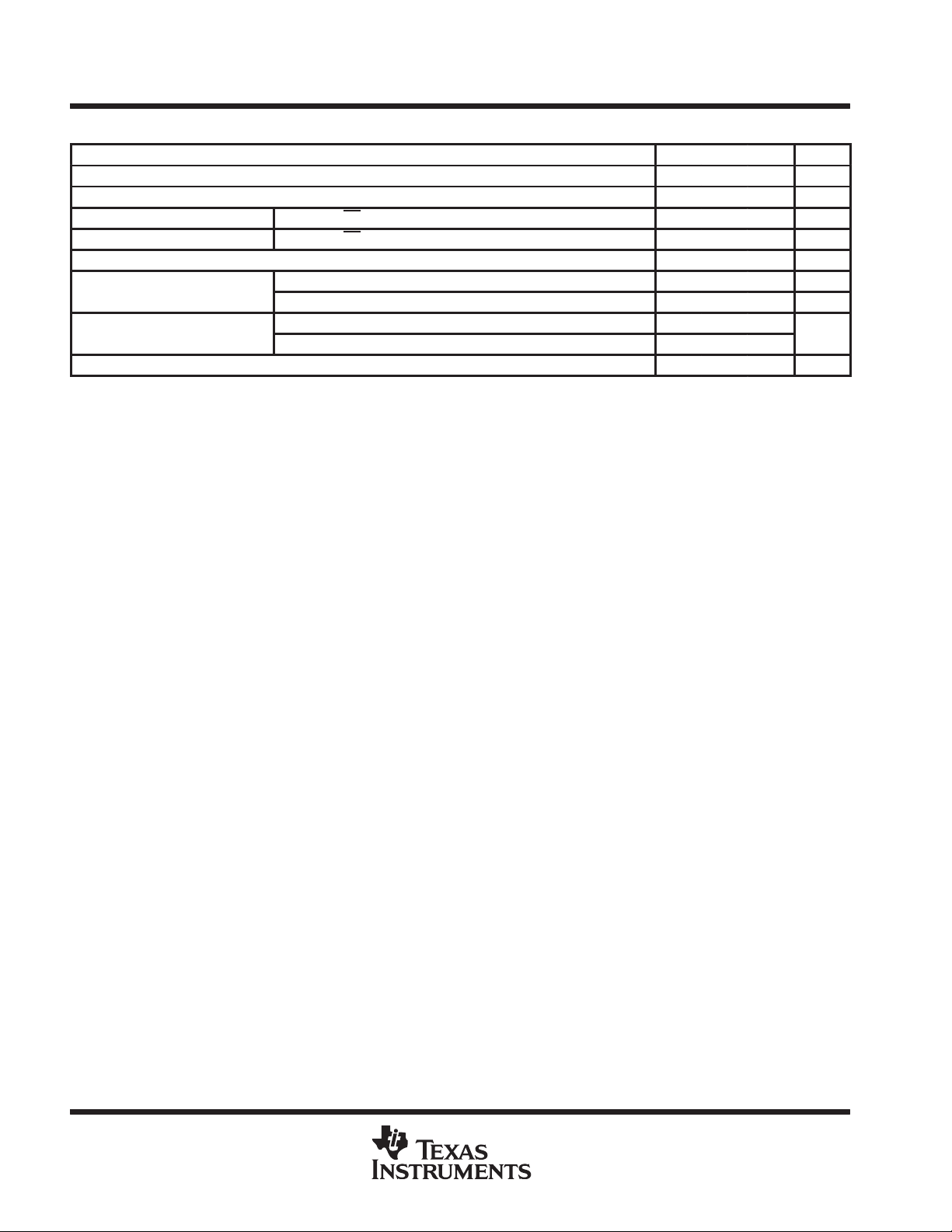
absolute maximum ratings over operating free-air temperature range (unless otherwise noted)
Supply voltage, V
Voltage range at any bus terminal –10 V to 15 V. . . . . . . . . . . . . . . . . . . . . . . . . . . . . . . . . . . . . . . . . . . . . . . . . . . .
Enable input voltage, V
Continuous total power dissipation See Dissipation Rating Table. . . . . . . . . . . . . . . . . . . . . . . . . . . . . . . . . . . . .
Operating free-air temperature range, T
Storage temperature range, T
Lead temperature 1,6 mm (1/16 inch) from case for 10 seconds 260°C. . . . . . . . . . . . . . . . . . . . . . . . . . . . . . .
†
Stresses beyond those listed under “absolute maximum ratings” may cause permanent damage to the device. These are stress ratings only, and
functional operation of the device at these or any other conditions beyond those indicated under “recommended operating conditions” is not
implied. Exposure to absolute-maximum-rated conditions for extended periods may affect device reliability.
NOTE 1: All voltage values, except differential input/output bus voltage, are with respect to network ground terminal.
(see Note 1) 7 V. . . . . . . . . . . . . . . . . . . . . . . . . . . . . . . . . . . . . . . . . . . . . . . . . . . . . . . . . . . . .
CC
5.5 V. . . . . . . . . . . . . . . . . . . . . . . . . . . . . . . . . . . . . . . . . . . . . . . . . . . . . . . . . . . . . . . . . . . .
I
0°C to 70°C. . . . . . . . . . . . . . . . . . . . . . . . . . . . . . . . . . . . . . . . . . . . . .
–65°C to 150°C. . . . . . . . . . . . . . . . . . . . . . . . . . . . . . . . . . . . . . . . . . . . . . . . . . .
stg
A
†
DISSIPATION RATING TABLE
T
≤ 25°C DERATING FACTOR T
POWER RATING ABOVE TA = 25°CAPOWER RATINGAPOWER RATING
D 725 mW 5.8 mW/°C 464 mW 261 mW
P 1100 mW 8.8 mW/°C 704 mW 396 mW
POST OFFICE BOX 655303 • DALLAS, TEXAS 75265
= 70_C T
= 105_C
3
SN75176A
High-level output current, I
Low-level output current, I
mA
DIFFERENTIAL BUS TRANSCEIVER
SLLS100A – JUNE 1984 – REVISED MA Y 1995
recommended operating conditions
MIN TYP MAX UNIT
Supply voltage, V
Voltage at any bus terminal (separately or common mode), VI or V
High-level input voltage, V
Low-level input voltage, V
Differential input voltage, VID (see Note 2) ±12 V
Operating free-air temperature, T
NOTE 2: Differential-input/output bus voltage is measured at the noninverting terminal A with respect to the inverting terminal B.
CC
IC
IH
IL
p
p
OH
OL
D, DE, and RE 2 V
D, DE, and RE 0.8 V
Driver –60 mA
Receiver –400 µA
Driver 60
Receiver 8
A
4.75 5 5.25 V
–7 12 V
0 70 °C
4
POST OFFICE BOX 655303 • DALLAS, TEXAS 75265
 Loading...