

Hitachi 55HB6T62U, 55289DLB Schematic
HITACHI
55HB6T62U
55289DLB
MB97
SERVICE MANUAL

TABLE OF CONTENTS
1. INTRODUCTION .......................................................................................................................................................... 2
2. T/T2/C/A Tuner (U74) ................................................................................................................................................... 3
3. S/S2 TUNER & DEMODULATOR (U90) OPTIONAL ............................................................................................... 4
4. AUDIO AMPLIFIER STAGES ..................................................................................................................................... 7
A. MAIN AMPLIFIER (U62)(6-8-10 W option) ...................................................................................... ........................ 7
B. MAIN AMPLIFIER (U91)(2.5 W option) ................................................................................................................... 9
C. HEADPHONE AMPLIFIER (U85) ............................................................................................................................. 11
5. POWER STAGE .......................................................................................................................................................... 13
6. MICROCONTROLLER ............................................................................................................................................... 25
A. MSTAR MSD88RKM2 (U95) .................................................................................................................................. 25
7. 2Gb DDR3 SDRAM ..................................................................................................................................................... 30
A. Hynix H5TQ2G63FFR-PBC (U72) ........................................................................................................................... 30
8. 2Gbit (256M x 8 bit) NAND Flash Memory ................................................................................................................ 32
A. MT29F2G08ABAEAWP (U80) ................................................................................................................................ 32
9. 16M-BIT [16M x 1] CMOS SERIAL FLASH EEPROM ............................................................................................ 34
A. KH25L1606EM2-12G Macronix SPI Flash (U81) .................................................................................................... 34
10. USB Interface ............................................................................................................................................................... 35
A. CY7C65642 (U73) .................................................................................................................................................. 36
11. CI Interface ................................................................................................................................................................... 38
12. Software Update ........................................................................................................................................................... 38
A. Main SW update ................................................................................................................................................... 38
13. Troubleshooting ............................................................................................................................................................ 39
A. No Backlight Problem ........................................................................................................................................... 39
B. CI Module Problem ..........................................................................................................
C. Staying in Stand-by Mode ..................................................................................................................................... 41
D. IR Problem ............................................................................................................................................................ 42
E. Keypad Touchpad Problems ................................................................................................................................. 42
F. USB Problems ........................................................................................................................................................ 43
G. No Sound Problem ................................................................................................................................................ 43
..................................... 40
H. Standby On/Off Problem ...................................................................................................................................... 44
İ. No Signal Problem ........................................................................................................... ...................................... 44
14. Service Menu Settings .................................................................................................................................................. 47
15. PLACEMENT OF BLOCKS ........................................................................................................................................ 52
16. General Block Diagram ................................................................................................................................................ 53
1

WARNING: It is necessary to remove the internal lead connector before removing the back cover of the
TV completely!
1. INTRODUCTION
17MB97 main board is driven by MStar SOC. This IC is a single chip iDTV solution that supports channel
decoding, MPEG decoding, and media-center functionality enabled by a high performance AV CODEC and
CPU.
Key features include:
Combo Front-End Demodulator
A multi standart A/V format decoder
The MACEpro video processor
Home theatre sound processor
Rich internet connectivity and completed digital home network solution
Dual-stream decoder for 3D contents
Mılti-purpose CPU for OS and multimedia
Peripheral and power management
Embedded DRAM
Supported peripherals are:
1 RF input VHF I, VHF III, UHF
1 Satellite input
1 Side AV (CVBS, R/L_Audio)
1 SCART socket(Common)
1 PC input(Common)
3 HDMI input
1 Common interface(Common)
1 Optic/ Quax S/PDIF output
1 Headphone(Common)
2 USB(1x common, 1x optional) and 2x internal USB for Wifi/Bluetooth
1 Ethernet-RJ45
1 External Touchpad(Common)
1 DVD(Optional)
2

2. T/T2/C/A TUNER (U74)
Description
The MxL661 is a highly integrated low-power silicon tuner IC that targets all global and digital cable standards.
Broadband input filtering and channel filtering have been completely integrated on-chip. This integration
enables a compact design resulting in small footprint, low Bill-Of-Material (BOM) cost, and low-power
consumption.
A signal at the 75ohm RF input is filtered and converted to a programmable IF output frequency. Automatic
Gain Control (AGC), LO generation, and channel selectivity functions are completey integrated on the chip. All
functions of the IC can be controlled using the I2C interface.
The MxL is available in a 4 mm x 4mm x 0.85mm3, 24-pin QFN package.
Features
Tuning range from 44MHz to 1002MHz
Programmable channel bandwidths of 6, 7, and 8MHz
Integrated channel filtering
Low power consumption with 3.3V and 1.8V dual-supply operation - 351 mW (digital terrestrial)
On-chip voltage regulator enables single supply 3.3V operation
Programmable IF frequency and IF spectrum inversion
Programmable RF to IF delay for ATV scrambling systems that relies on the H-Sync method
Optioanl balun-less application note for cost-sensitive applications
Reference clock output available for re-use by demodulators and additional tuners in multi-channel
Input power reporting
Open-drain General Purpose Output GPO available for controlling off-chip circuitry
I
applications
2
C compatible digital control interface
RoHS compliance
3
Figure: Pin description
Table: Pin functions
3. S/S2 TUNER & DEMODULATOR (U90) OPTIONAL
Description
The M88RS6000 is highly single-Chip DVB-S2/S receiver. The device is consisting of tuner, a demodulator
and an LNB controller. It is fully compliant with the DVB-S2 and DVB-S standards by supporting
QPSK,(PSK,16APSK and 32APSK demodulator schemes.
The tuner is the device an RF signal in the frequency range from 950 Mhz to 2150 Mhz and down-convert the
signal directly to analog baseband signal, which will be converted to a digital signal in the advanced ADC.
After the ADC, the digital signal will be demodulated in the demodulator, related errors generated during
transmission will be corrected at this stage and finally an MPEG transport stream will be delivered in serial,
parallel or DVB-CI format.
4
Figure: Pin description
5
FEATURES
6

4. AUDIO AMPLIFIER ST AGES
A. MAIN AMPLIFIER (U62)(6-8-10 W option)
Description
AD82587D is a digital audio amplifier capable of driving a pair of 8 ohm, 20W or a single 4ohm, 40W speaker,
both which operate with play music at a 24V supply without external heat-sink or fan requirement.
Using I2C digital control interface, the user can control AD82587D’s input format selection, mute and volume
control functions. AD82587D has many built-in protection circuits to safeguard AD82587D from connection
errors.
Features
16/18/20/24-bit input with I
PSNR & DR(A-weighting) Loudspeaker: 97dB (PSNR), 105dB (DR) @ 24V
Multiple sampling frequencies (Fs)
o 32kHz / 44.1kHz / 48kHz and
2
S, Left-alignment and Right-alignment data format
o 64kHz / 88.2kHz / 96kHz and
o 128kHz/176.4kHz/192kHz
System clock = 64x, 128x, 256x, 384x, 512x, 768x,1024x Fs
o 256x~1024x Fs for 32kHz / 44.1kHz / 48kHz
o 128x~512x Fs for 64kHz / 88.2kHz / 96kHz
o 64x~256x Fs for 128kHz /176.4kHz/192kHz
Supply voltage
o 3.3V for digital circuit
o 10V~26V for loudspeaker driver
Loudspeaker output power for Stereo@ 24V
o 10W x 2ch into 8_ @ 0.16% THD+N
o 15W x 2ch into 8_ @ 0.18% THD+N
o 20W x 2ch into 8_ @ 0.24% THD+N
Loudspeaker output power for Mono@ 24V
o 20W x 1ch into 4_ @ 0.17% THD+N
o 30W x 1ch into 4_ @ 0.2% THD+N
o 40W x 1ch into 4_ @ 0.24% THD+N
Sounds processing including:
o Volume control (+24dB~-103dB, 0.125dB/step)
o Dynamic range control
o Power clipping
o Channel mixing
7
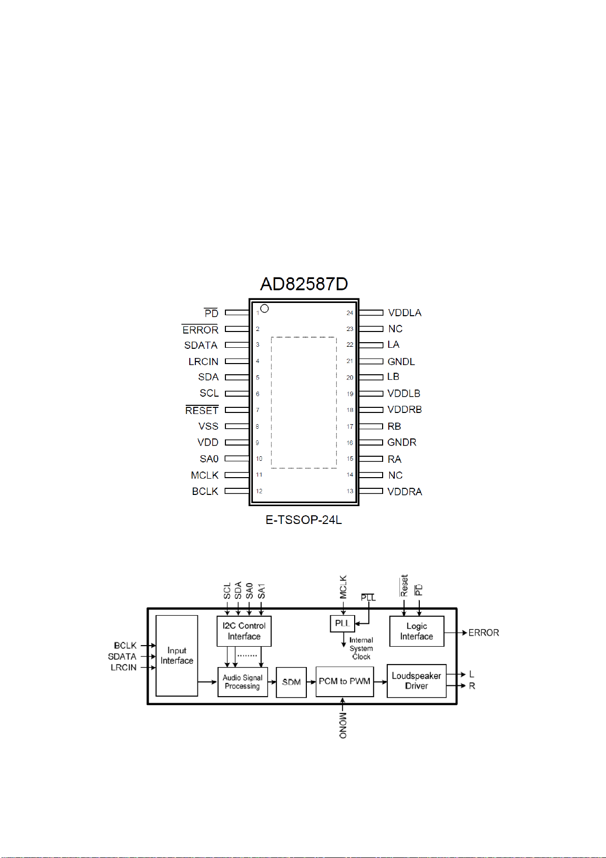
o User programmed noise gate with hysteresis window
o DC-blocking high-pass filter
Anti-pop design
Short circuit and over-temperature protection
I2C control interface with selectable device address
Internal PLL
LV Under-voltage shutdown and HV Under-voltage
detection
Power saving mode
Dynamic temperature control
8
Figure: Pin description
Figure: Functional Block Diagram
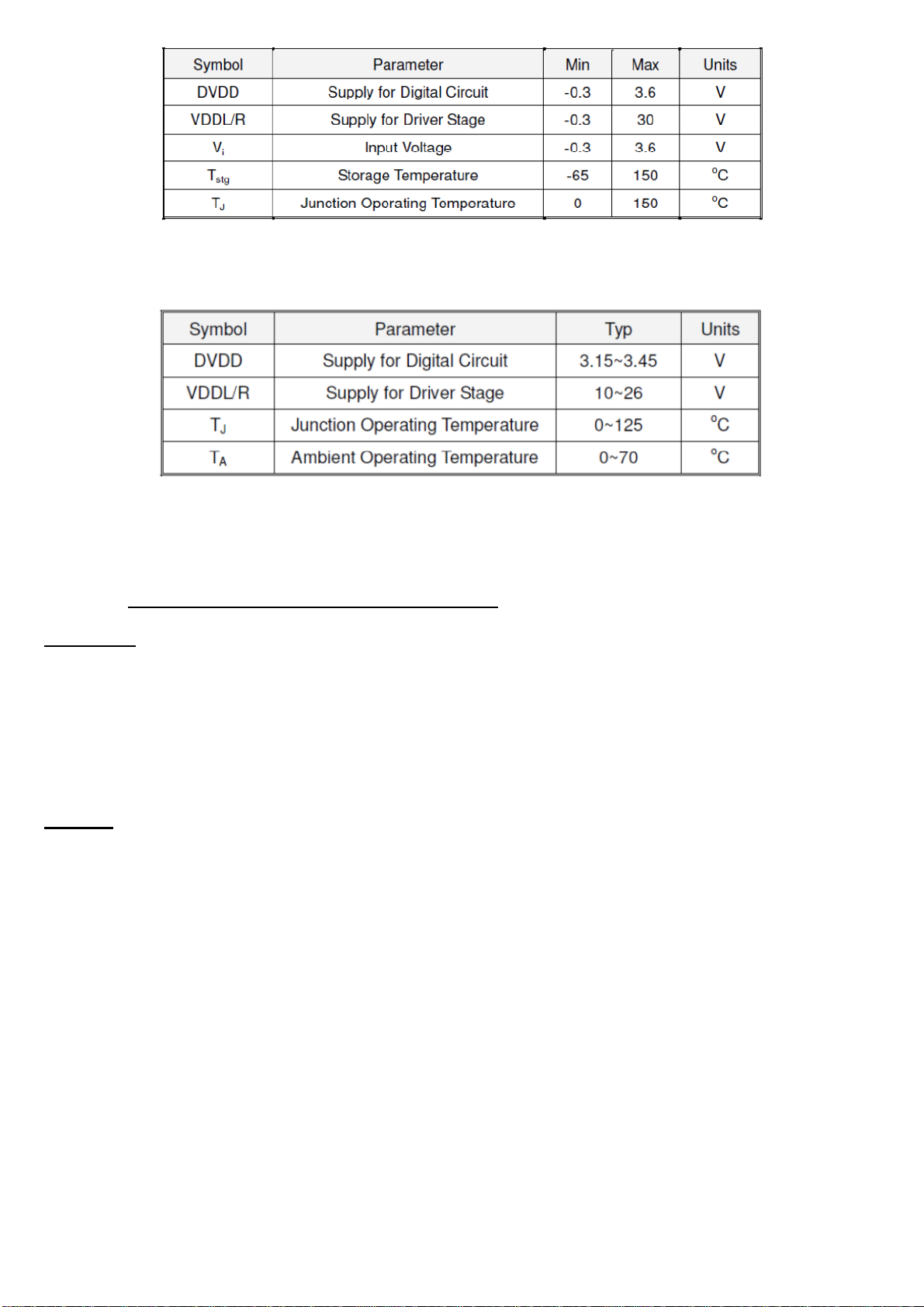
Table: Absolute Maximum Ratings
Table: Recommended Operating Conditions
B. MAIN AMPLIFIER (U91)(2.5 W option)
Description
The AD52010 is a 3.0W stereo, filter-less class-D audio amplifier. Operating with 5.0V loudspeaker driver
supply, it can deliver 3.0W output power into 4 ohm loudspeaker within 10% THD+N or 2.6W at 1% THD+N.
The AD52010 is a stereo audio amplifier with high efficiency and suitable for the notebook computer, and
portable multimedia device.
Features
Supply voltage range: 2.5 V to 5.5 V
Support single-ended or differential analog input
Low Quiescent Current
Low Output Noise
Low shut-down current
Short power-on transient time
Internal pull-low resistor on shut-down pins
Short-circuit protection
Over-temperature protection
Loudspeaker power within 10% THD+N
o 1.78W/ch into 8 ohm loudspeaker
9
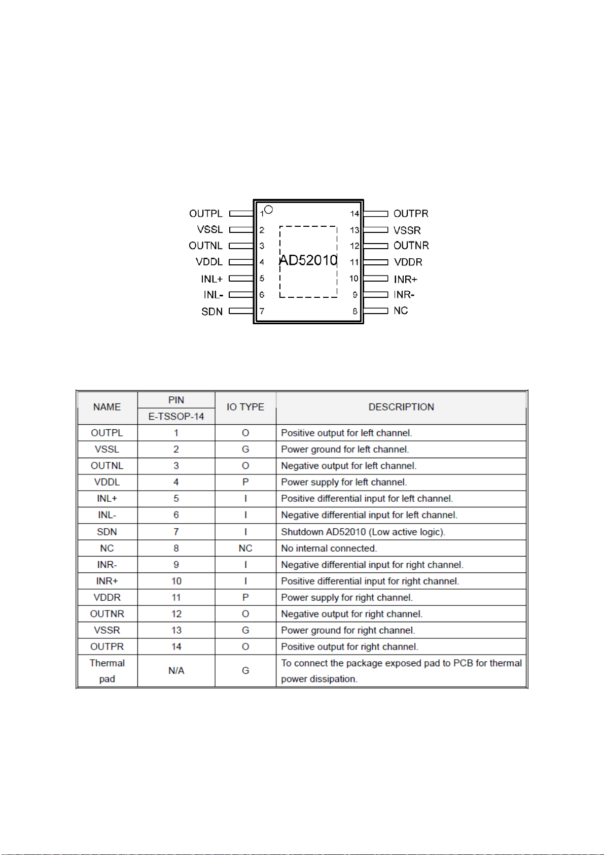
o >3W/ch into 4 ohm loudspeaker
Loudspeaker efficiency
o 93% @ 8 ohm, THD+N=10%
o 85% @ 4 ohm, THD+N=10%
E-TSSOP-14L package
Integrated Feedback Resistor of 300kW
Figure: Pin description
10
Table:Pin functions

Table: Recommended operating conditions
C. HEADPHONE AMPLIFIER (U85)
Description
The AD22657B is a 2-Vrms cap-less stereo line driver. The device is ideal for single supply electronics. Cap-
less design can eliminate output dc-blocking capacitors for better low frequency response and save cost.
The AD22657B is capable of delivering 2-Vrms output into a 10k ohm load with 3.3V supply. The gain settings
can be set by users from 1V/V to 10V/V externally. The AD22657B has under voltage protection to prevent
POP noise. Build-in shutdown control and de-pop control sequence also help AD22657B to be a pop-less
device.
The AD22657B is available in a 10-pin MSOP package.
Features
Operation Voltage: 3V to 3.6V
Cap-less Output
o Eliminates Output Capacitors
o Improves Low Frequency Response
o Reduces POP/Clicks
Low Noise and THD
o Typical SNR 107dB
o Typical Vn 7uVrms
o Typical THD+N < 0.02%
Maximum Output Voltage Swing into 2.5k Load
o 2Vrms at 3.3V Supply Voltage
Single-ended Input
External Gain Setting from 1V/V to 10V/V
Fast Start-up Time: 0.5ms
Integrated De-Pop Control
External Under Voltage Protection
Thermal Protection
11
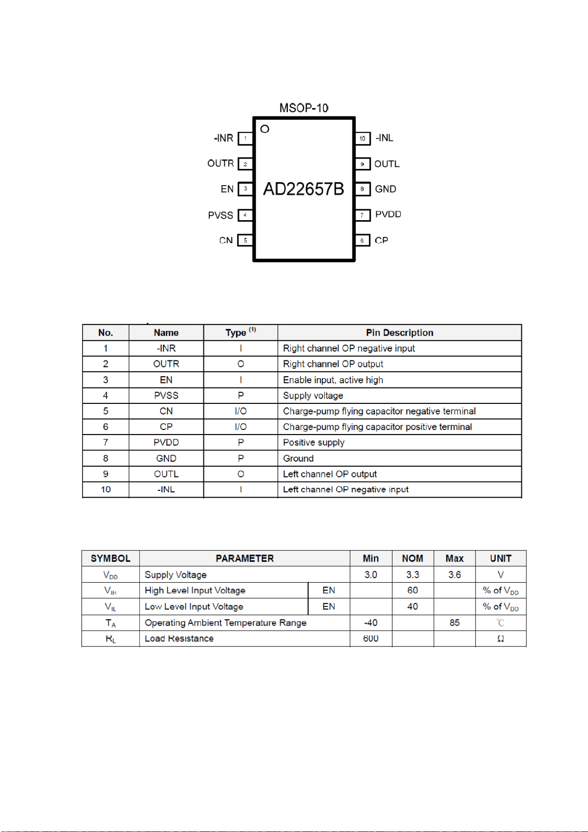
Less External Components Required
+/-8kV IEC ESD Protection at line outputs
Figure: Pin description
12
Table: Pin functions
Table: Recommended operating conditions
5. POWER STAGE
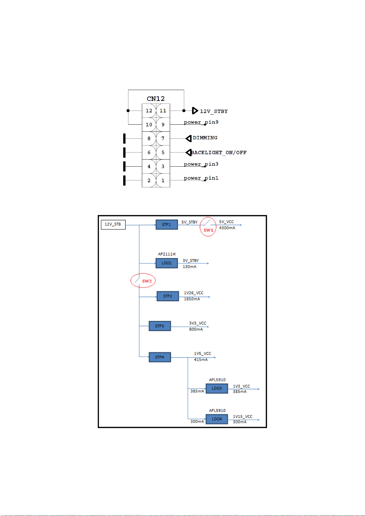
Power socket is used for taking voltages which are 12V_stby and 24V (VDD_Audio for 10W option). These
voltages are produced in power card. Also socket is used for giving dimming, backlight and stand-by signals
with power card. It is shown in figure.
Figure: Power socket and power options
List of the components are:
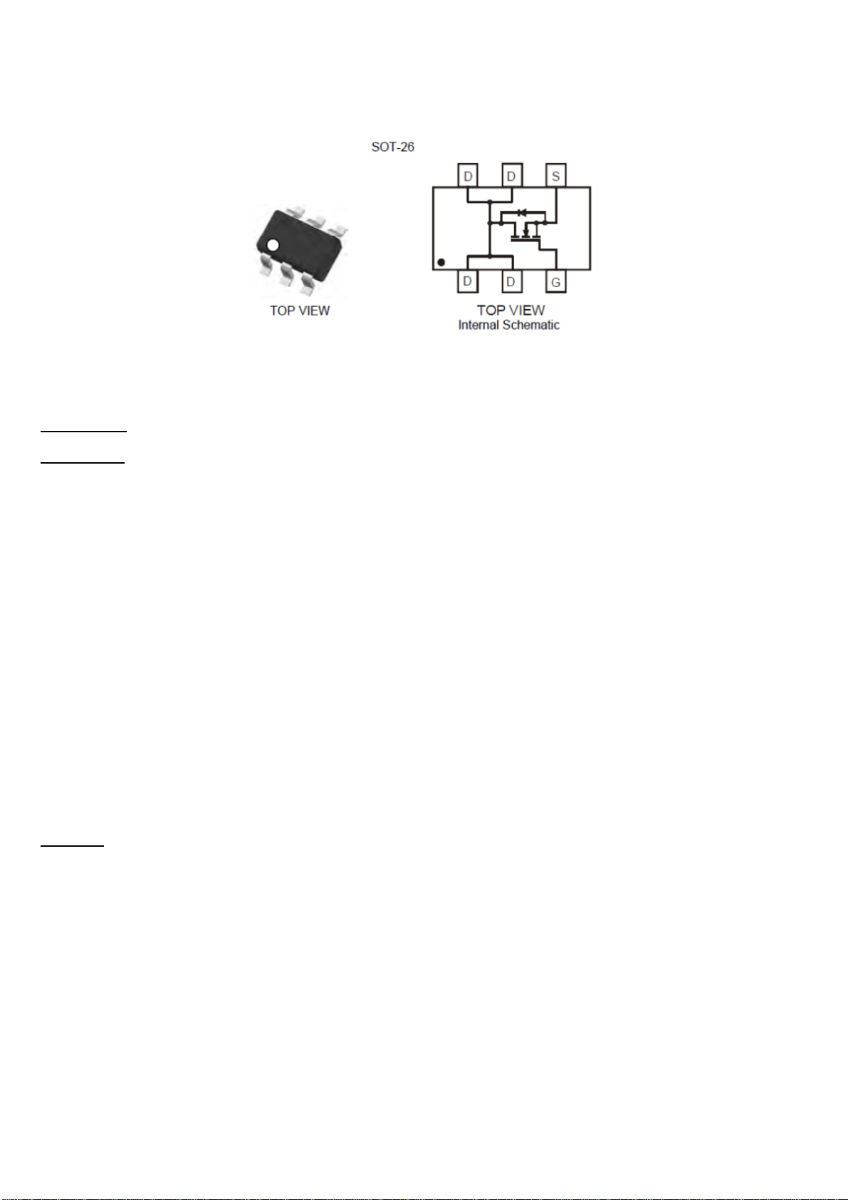
SW1(Q56) → DMG6402LDM
SW2(Q44) → FDC642P
13
STP1(U63) → RT7278G(12V panel option)
STP1(U63) → TPS54528(5V panel option)
STP2(U88) → MP2315
STP3(U70) → RT7257
STP4(U96) → RT7237
LDO1(U94) → LM1117
LDO3(U89) → APL5910
LDO4(U65) → APL5910
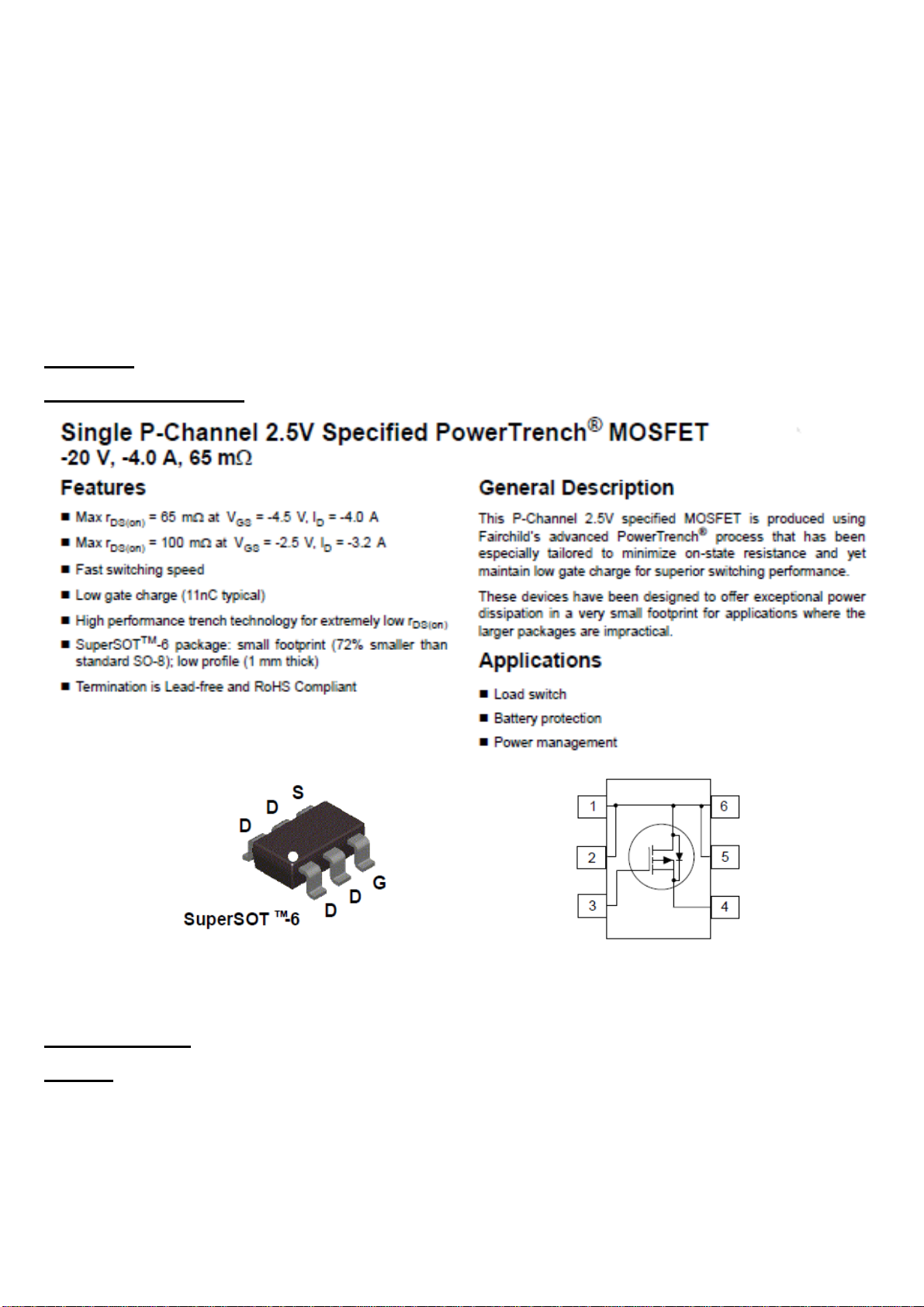
FDC642P
Description and Features
DMG6402LDM
Features
Low RDS(ON)
Low Input Capacitance
Fast Switching Speed
Figure: Pin description
14
Low Input/Output Leakage
Lead Free By Design/RoHS Compliant (Note 1)
Qualified to AEC-Q101 Standards for High Reliability
Figure: Pin description
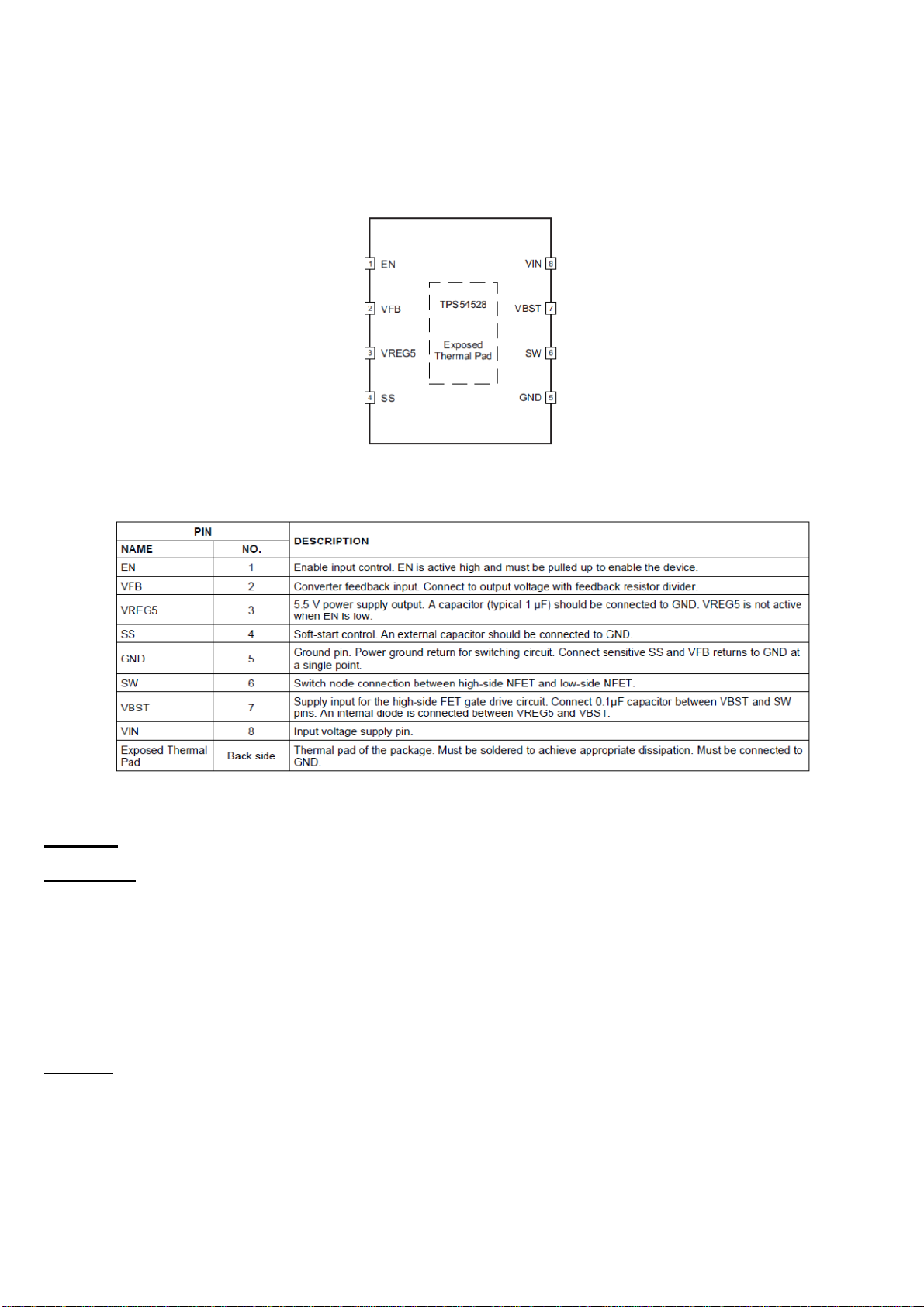
TPS54528
Description
The TPS54528 is an adaptive on-time D-CAP2™ mode synchronous buck converter. The TPS54528 enables
system designers to complete the suite of various end-equipment power bus regulators with a cost effective, low
component count, low standby current solution. The main control loop for the TPS54528 uses the D-CAP2™
mode control that provides a fast transient response with no external compensation components. The adaptive
on-time control supports seamless transition between PWM mode at higher load conditions and Eco-mode™
operation at light loads. Eco-mode™ allows the TPS54528 to maintain high efficiency during lighter load
conditions. The TPS54528 also has a proprietary circuit that enables the device to adopt to both low equivalent
series resistance (ESR) output capacitors, such as POSCAP or SP-CAP, and ultra-low ESR ceramic capacitors.
The device operates from 4.5-V to 18-V VIN input. The output voltage can be programmed between 0.76 V
and 6.0 V. The device also features an adjustable soft start time. The TPS54528 is available in the 8-pin DDA
package, and designed to operate from –40 C to 85 C.
Features
D-CAP2™ Mode Enables Fast Transient Response
Low Output Ripple and Allows Ceramic Output Capacitor
Wide VIN Input Voltage Range: 4.5 V to 18 V
Output Voltage Range: 0.76 V to 6.0 V
Highly Efficient Integrated FETs Optimized for Lower Duty Cycle Applications
o 65 mΩ (High Side) and 36 mΩ (Low Side)
High Efficiency, less than 10 μA at shutdown
High Initial Bandgap Reference Accuracy
15
Adjustable Soft Start
Pre-Biased Soft Start
650-kHz Switching Frequency (fSW)
Cycle By Cycle Over Current Limit
Auto-Skip Eco-mode™ for High Efficiency at Light Load
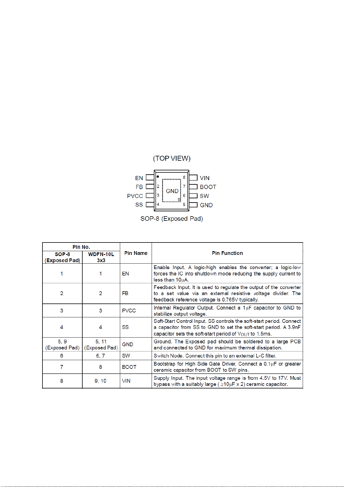
Figure: Pin description
Table: Pin functions
RT7278
Description
The RT7278 is a synchronous step down converter with Advanced Constant On-Time (ACOTTM) mode
control. The ACOTTM provides a very fast transient response with few external components. The low
impedance internal MOSFET supports high efficiency operation with wide input voltage range from 4.5V to
17V. The proprietary circuit of the RT7278 enables to support all ceramic capacitors. The output voltage can be
adjustable between 0.8V and 8V. The soft-start is adjustable by an external capacitor.
Features
TM
ACOT
Mode Enables Fast Transient Response
4.5V to 17V Input Voltage Range
3A Output Current
60mΩ Internal Low Site N-MOSFET
16
Advanced Constant On-Time Control
Support All Ceramic Capacitors
Up to 95% Efficiency
700kHz Switching Frequency
Adjustable Output Voltage from 0.8V to 8V
Adjustable Soft-Start
Cycle-by-Cycle Current Limit
Input Under Voltage Lockout
Thermal Shutdown Protection
RoHS Compliant and Halogen Free
Figure: Pin description
17
Table: Pin functions
MP2315
Description
The MP2315 is a high frequency synchronous rectified step-down switch mode converter with built in internal
power MOSFETs. It offers a very compact solution to achieve 3A continuous output current over a wide input
supply range with excellent load and line regulation. The MP2315 has synchronous mode operation for higher
efficiency over output current load range. Current mode operation provides fast transient response and eases
loop stabilization. Full protection features include OCP and thermal shut down. The MP2315 requires a
minimum number of readily available standard external components and is available in a space saving 8-pin
TSOT23 package.
Features
Wide 4.5V to 24V Operating Input Range
3A Load Current
90mΩ/40mΩ Low Rds(on) Internal Power MOSFETs
Low Quiescent Current
High Efficiency Synchronous Mode Operation
Fixed 500kHz Switching Frequency
Frequency Sync from 200kHz to 2MHz External Clock
AAM Power Save Mode
Internal Soft Start
OCP Protection and Hiccup
Thermal Shutdown
Output Adjustable from 0.8V
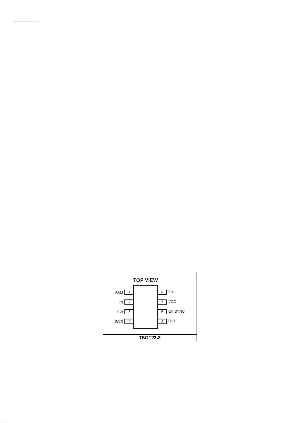
Available in an 8-pin TSOT-23 package
18
Figure: Pin description
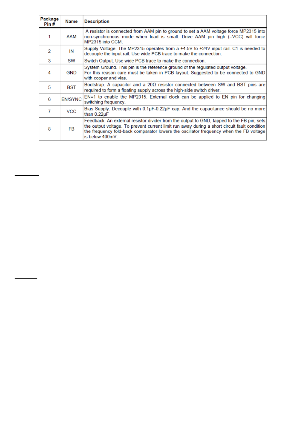
Table: Pin functions
RT7257
Description
The RT7257G is a high efficiency, monolithic synchronous step-down DC/DC converter that can deliver up to
3A output current from a 4.5V to 18V input supply. The RT7257G's current mode architecture and external
compensation allow the transient response to be optimized over a wide input voltage range and loads. Cycle-by-
cycle current limit provides protection against shorted outputs, and soft-start eliminates input current surge
during start-up. The RT7257G also provides under voltage protection and thermal shutdown protection. The
low current (<3uA) shutdown mode provides output disconnection, enabling easy power management in
battery-powered systems. The RT7257G is available in an SOP-8 (Exposed Pad) package.
Features
±1.5% High Accuracy Reference Voltage
4.5V to 18V Input Voltage Range
3A Output Current
Integrated N-MOSFET Switches
Current Mode Control
Fixed Frequency Operation: 800kHz
Output Adjustable from 0.8V to 12V
Up to 95% Efficiency
Programmable Soft-Start
Stable with Low ESR Ceramic Output Capacitors
Cycle-by-Cycle Current Limit
19
Input Under Voltage Lockout
Output Under Voltage Protection
Thermal Shutdown Protection
RoHS Compliant and Halogen Free
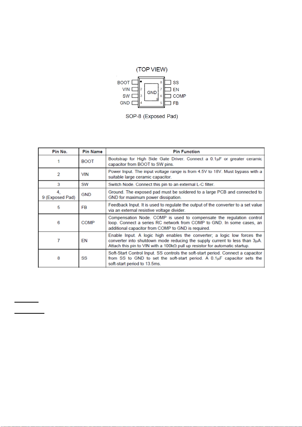
Figure: Pin description
Table: Pin functions
RT7237
Description
The RT7237C is a high efficiency, monolithic synchronous step-down DC/DC converter that can deliver up to
2A output current from a 4.5V to 18V input supply. The RT7237C's current mode architecture and external
compensation allow the transient response to be optimized over a wide input range and loads. Cycle-bycycle
current limit provides protection against shorted outputs, and soft-start eliminates input current surge during
start-up. The RT7237C also provides under voltage protection and thermal shutdown protection. The low
current (<3μA) shutdown mode provides output disconnection, enabling easy power management in battery-
powered systems. The RT7237C is available in an SOP-8 (Exposed Pad) package.
20
 Loading...