

Hitachi 49HK6T74U, 49293DLB Schematic
HITACHI
49HK6T74U
49293DLB
MB120
SERVICE MANUAL

Table of Contents
1. INTRODUCTION .......................................................................................................................................................... 2
2. TUNER ........................................................................................................................................................................... 3
A. SI2151 Terrestrial and Cable TV Tuner: ..................................................................................................................... 3
B. M88TS2022 Satellite Tuner ........................................................................................................................................ 5
3. AUDIO AMPLIFIER STAGES ...................................................................................................................................... 6
A. MAIN AMPLIFIER (U8) (10W/12W options) ............................................................................................................... 6
B. SUBWOOFER AMPLIFIER (U9) (12 W) ........................................................................................................................ 8
C. HEADPHONE AMPLIFIER (U59) ................................................................................................................................ 10
D. SUBWOOFER PREAMPLIFIER (U30) .......................................................................................................................... 12
E. SCART AUDIO AMPLIFIER (U31) ............................................................................................................................... 12
4. POWER STAGE ........................................................................................................................................................... 12
A. TPS54528 ................................................................................................................................................................. 13
B. TPS54628 ................................................................................................................................................................. 15
C. TPS54821 ................................................................................................................................................................. 17
D. FDS4685 ................................................................................................................................................................... 19
E. NTGS3446 ................................................................................................................................................................ 20
F. APL5910 ................................................................................................................................................................... 21
G. LM1117 .................................................................................................................................................................... 23
5. MICROCONTROLLER (MSTAR MSD95M0D) ........................................................................................................ 24
6. VIDEO BACK-END PROCESSOR (MSTAR) ........................................................................................................... 31
MST7410FE ................................................................................................................................................................... 31
7. 2Gb DDR3 SDRAM ..................................................................................................................................................... 34
Hynix H5TQ2G63GFR .................................................................................................................................................... 34
8. 4Gb DDR3L SDRAM ................................................................................................................................................... 35
Hynix H5TQ4G63GFR .................................................................................................................................................... 35
9. 32GBIT (4G X 8 BIT) NAND FLASH MEMORY ..................................................................................................... 37
MT29F4G08ABAEAWP .................................................................................................................................................. 37
10.
16M-BIT [16M x 1] CMOS SERIAL FLASH EEPROM ............................................................................................ 39
A. MX25L1606E SPI Flash ............................................................................................................................................. 39
B. M25Q32FV SPI Flash ................................................................................................................................................ 41
11. DEMODULATOR STAGE .......................................................................................................................................... 43
12. LNB SUPPLY AND CONTROL IC ............................................................................................................................ 46
TPS65233 ...................................................................................................................................................................... 46
13. SOFTWARE UPDATE ................................................................................................................................................ 47
Main SW update ........................................................................................................................................................... 47
1

14. TROUBLESHOOTING ................................................................................................................................................ 48
A. No Backlight Problem .............................................................................................................................................. 48
B. CI Module Problem .................................................................................................................................................. 50
C. Staying in Stand-by Mode ........................................................................................................................................ 52
D. IR Problem ................................................................................................................................................................ 54
E. Keypad Touchpad Problems .................................................................................................................................... 55
F. USB Problem s ............................................................................................................... ............................................ 56
G. No Sound Problem ................................................................................................................................................... 57
H. Standby On/Off Problem ......................................................................................................................................... 58
İ. No Signal Problem ........................................................................................................... ......................................... 58
15. GENERAL BLOCK DIAGRAM ................................................................................................................................. 59
1. INTRODUCTION
17MB120 main board is driven by MStar SOC. This IC is a single chip iDTV solution that supports channel
decoding, MPEG decoding, and media-center functionality enabled by a high performance AV CODEC and
CPU. This IC also supports 4K2K (UHD).
Key features includes,
Combo Front-End Demodulator
A multi standart A/V format decoder
The MACEpro video processor
Home theatre sound processor
Internet and Variety of Connectivity Support
Dual-stream decoder for 3D contents
Multi-purpose CPU for OS and multimedia
Peripheral and power management
Supported peripherals are:
1 RF input VHF I, VHF III, UHF
1 Satellite input
1 Side AV (CVBS, R/L_Audio)
1 SCART socket(Common)
1 YPbPr / Back S-Video(Common)
1 PC input(Common)
4 HDMI input(Common)
1 Common interface(Common)
1 Optic S/PDIF output(Common)
1 Stereo audio input for PC(Common)
1 Subwoofer output(Common)
1 Headphone(Common)
1x USB3.0 and 2xUSB2.0(Common)
1 Ethernet-RJ45 (Common)
1 External Touchpad(Common)
2
2. TUNER
A. SI2151 TERRESTRİAL AND CABLE TV TUNER:
Description:
The Si2151 is Silicon Labs' sixth-generation hybrid TV tuner supporting all worldwide terrestrial and cable
TV standards. Requiring no external balun, SAW filters, wirewound inductors or LNAs, the Si2151 offers the
lowest-cost BOM for a hybrid TV tuner. Also included are an integrated power-on reset circuit and an option
for single power supply operation. As with prior-generation Silicon Labs TV tuners, the Si2151 maintains very
high linearity and low noise to deliver superior picture quality and a higher number of received stations when
compared to other silicon tuners. The Si2151 offers increased immunity to WiFi and LTE interference,
eliminating the need for external filtering. For the best performance with next-generation digital TV standards,
such as DVB-T2/C2, the Si2151 delivers industry-leading phase noise performance.
Features:
Worldwide hybrid TV tuner
o Analog TV: NTSC, PAL/SECAM
o Digital TV: ATSC/QAM, DVBT2/T/C2/C, ISDB-T/C, DTMB
1.7 MHz, 6 MHz, 7 MHz, 8 MHz, and 10 MHz channel bandwidths
42-1002 MHz frequency range
Industry-leading margin to A/74, NorDig, DTG, ARIB, EN55020, OpenCable™,DTMB
Lowest BOM for a hybrid TV tuner
o No balun, SAW filters, or external inductors required
o Increased ESD protection on 4pins
Best-in-class real-world reception
o Lowest phase noise
o High Wi-Fi and LTE immunity
Low power consumption
o 3.3 V and 1.8 V power supplies
o Integrated 1.8 V LDO for 3.3 V singlesupply operation
Integrated power-on reset circuit
Standard CMOS process
3x3 mm, 24-pin QFN package
RoHS compliant
3
Figure 1.1 Si2151 Pin description
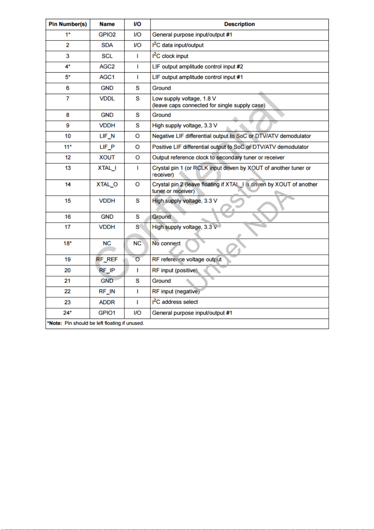
Table 1.1 Pin Functions
4
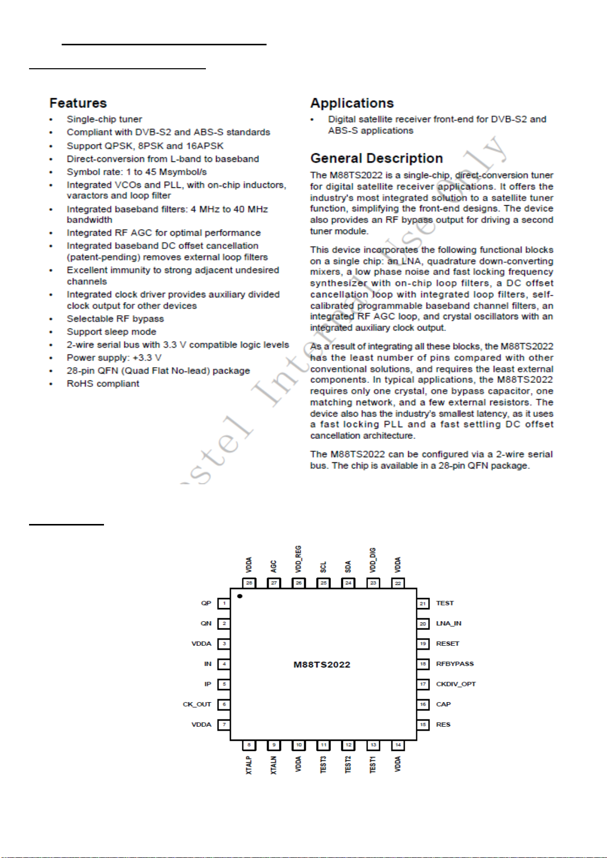
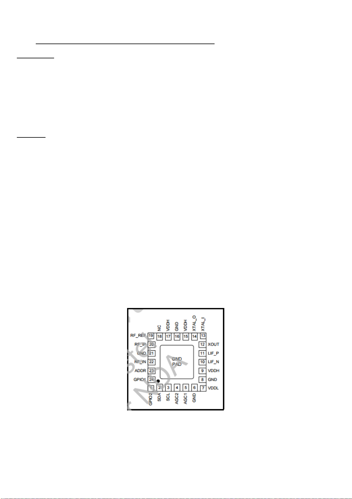
B. M88TS2022 SATELLİTE TUNER
Features and General Description
Pin Assigment
5
Absolute Maximum Ratings and Recommended Operating Conditions
3. AUDIO AMPLIFIER STAGES
A. MAIN AMPLIFIER (U8) (10W/12W OPTİONS)
Description
AD82587D is a digital audio amplifier capable of driving a pair of 8 ohm, 20W or a single 4 ohm, 40W
speaker, both which operate with play music at a 24V supply without external heat-sink or fan requirement.
Using I2C digital control interface, the user can control AD82587D’s input format selection, DRC (dynamic
range control), mute and volume control functions. AD82587D has many built-in protection circuits to
safeguard AD82587D from connection errors.
Features
16/18/20/24-bit input with I
PSNR & DR(A-weighting) Loudspeaker: 97dB (PSNR), 105dB (DR) @ 24V
Multiple sampling frequencies (Fs)
32kHz / 44.1kHz / 48kHz and
64kHz / 88.2kHz / 96kHz and
128kHz/176.4kHz/192kHz
System clock = 64x, 128x, 256x, 384x, 512x, 768x,1024x Fs
256x~1024x Fs for 32kHz / 44.1kHz / 48kHz
128x~512x Fs for 64kHz / 88.2kHz / 96kHz
64x~256x Fs for 128kHz /176.4kHz/192kHz
Supply voltage
3.3V for digital circuit
10V~26V for loudspeaker driver
2
S, Left-alignment and Right-alignment data format
6
Loudspeaker output power for Stereo@ 24V
10W x 2ch into 8_ @ 0.16% THD+N
15W x 2ch into 8_ @ 0.18% THD+N
20W x 2ch into 8_ @ 0.24% THD+N
Loudspeaker output power for Mono@ 24V
20W x 1ch into 4_ @ 0.17% THD+N
30W x 1ch into 4_ @ 0.2% THD+N
40W x 1ch into 4_ @ 0.24% THD+N
Sounds processing including:
Volume control (+24dB~-103dB, 0.125dB/step)
Dynamic range control
Power clipping
Channel mixing
User programmed noise gate with hysteresis window
DC-blocking high-pass filter
Anti-pop design
Short circuit and over-temperature protection
I2C control interface with selectable device address
Internal PLL
LV Under-voltage shutdown and HV Under-voltage
detection
Power saving mode
Dynamic temperature control
7
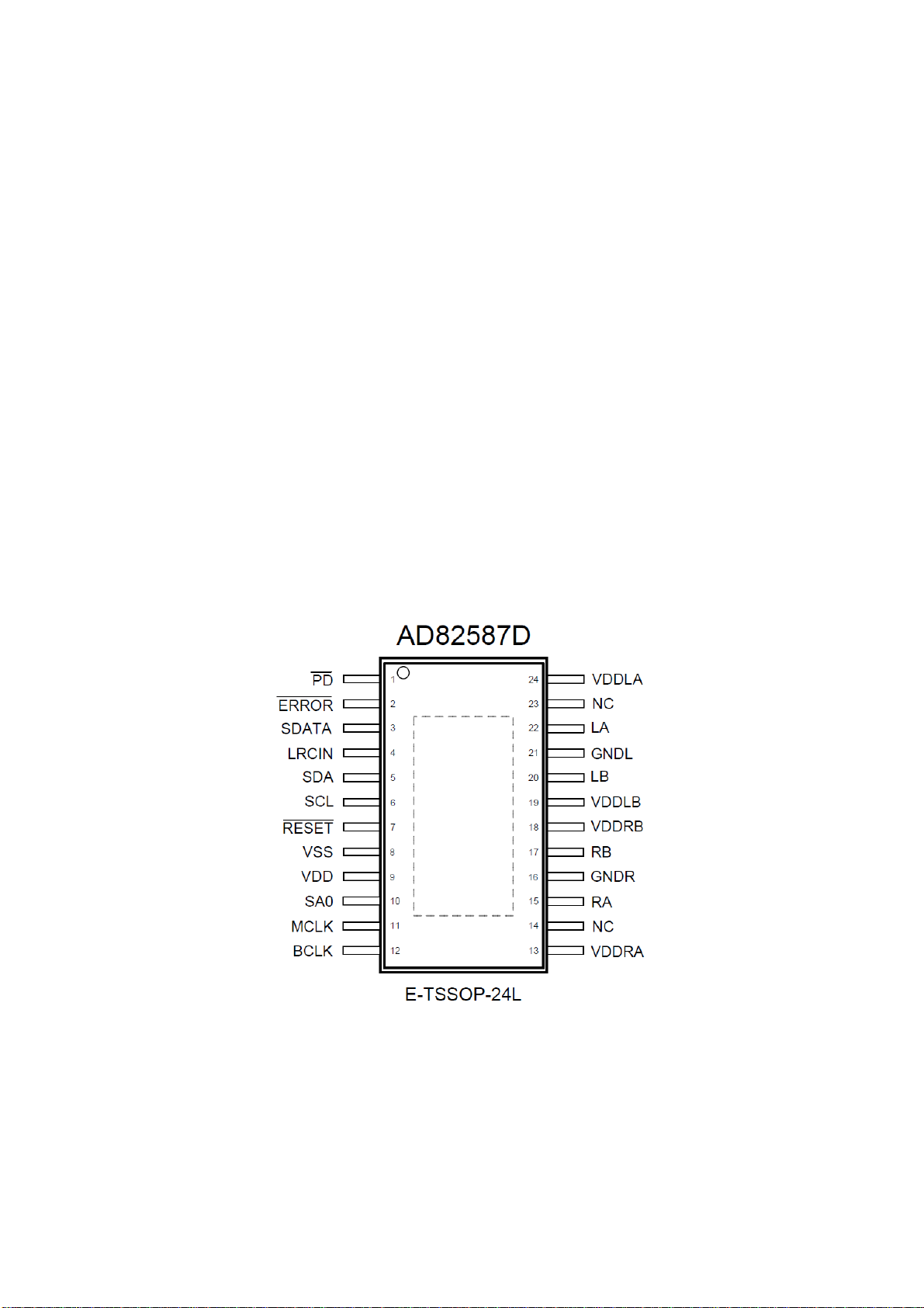
Figure 3.2: Pin description
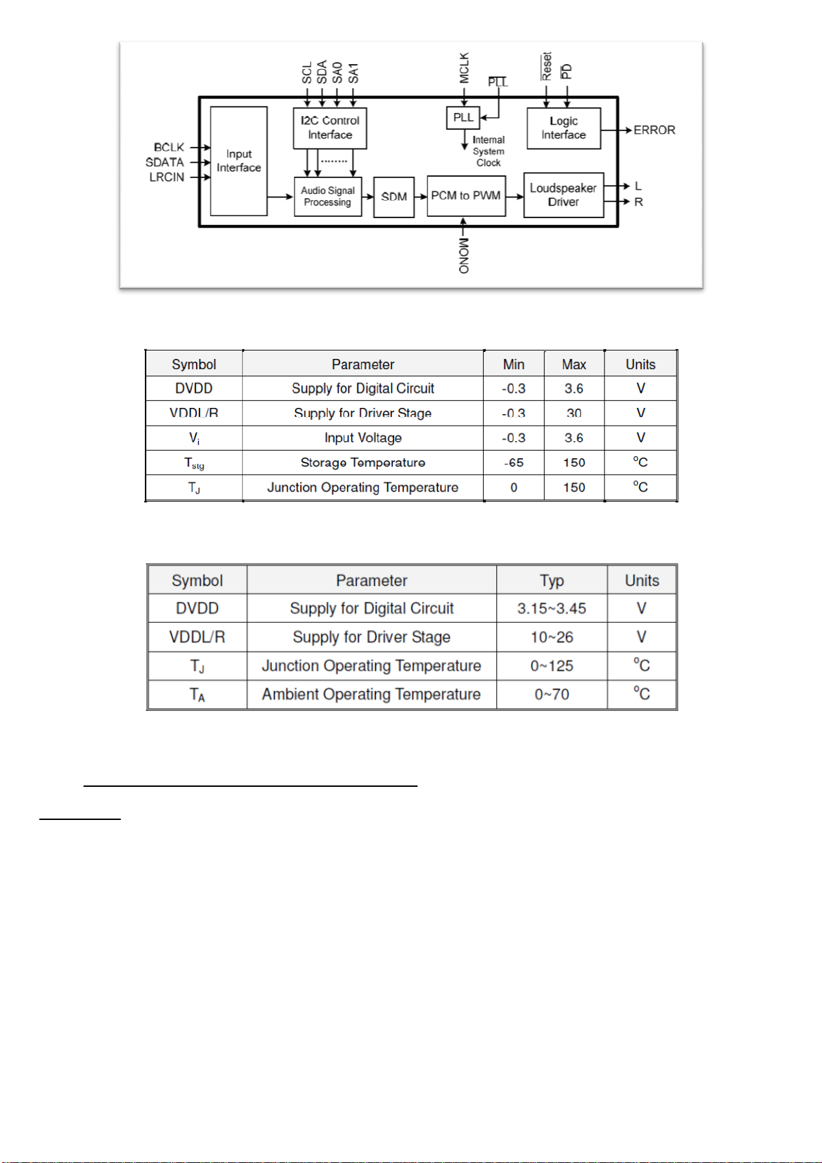
Figure 3.3: Functional Block Diagram
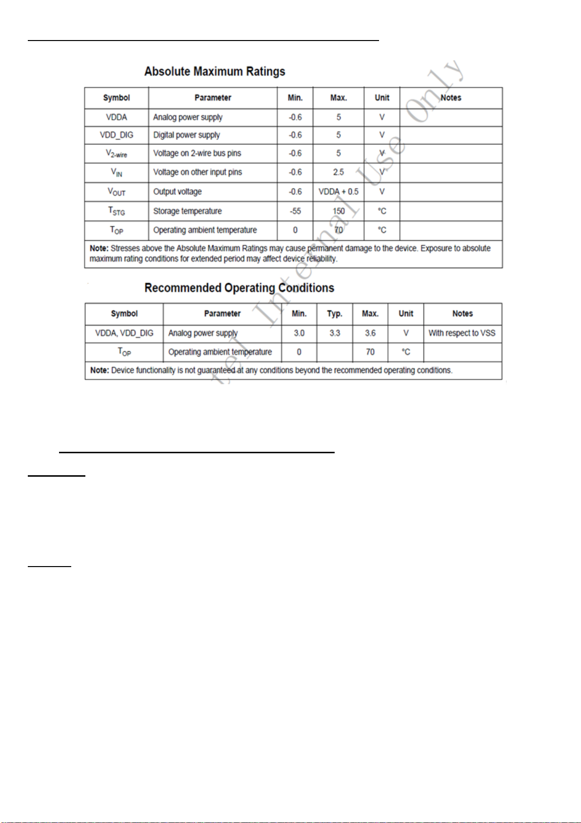
Table3.1: Absolute Maximum Ratings
Table3.2: Recommended Operating Conditions
B. SUBWOOFER AMPLIFIER (U9) (12 W)
Description
AD82586C is a digital audio amplifier capable of driving a pair of 8 ohm, 20W operating at 24V supply
without external heat-sink or fan requirement with play music.
AD82586C has 20 bands EQ function and can operate 20W stereo or 40W mono optionally.
AD82586C can provide advanced audio processing capabilities, such as volume control, 20 bands speaker
EQ, audio mixing, 3D surround and DRC (dynamic range control). These functions are fully programmable via
a simple I2C control interface.
Robust protection circuits are provided to protect AD82586C from damage due to accidental erroneous
operating condition. AD82586C is more tolerant to noise and PVT (Process, Voltage, and Temperature)
variation than the analog Class-AB or Class-D audio amplifier counterpart implemented by analog circuit
design. AD82586C is pop free during instantaneous power switch because of its built-in, robust anti-pop circuit.
8
Features
16/18/20/24-bits input with I
2
S, Left-alingment and Right-alingment data format
PSNR & DR (A-weighting) Loudspeaker: 99dB (PSNR), 104dB (DR) @24V
Multiple sampling frequencies (Fs)
32kHz / 44.1kHz / 48kHz and
64kHz / 88.2kHz / 96kHz and
128kHz / 176.4kHz / 192kHz
System clock = 64x, 128x, 192x, 256x, 384x, 512x, 576x, 768x, 1024x Fs
64x~1024x Fs for 32kHz / 44.1kHz / 48kHz
64x~512x Fs for 64kHz / 88.2kHz / 96kHz
64x~256x Fs for 128kHz / 176.4kHz / 192kHz
Supply voltage
3.3V for digital circuit
10V~26V for loudspeaker driver
Loudspeaker output power at 24V
10W x 2CH into 8 ohm @0.17% THD+N for stereo
20W x 2CH into 8 ohm @0.26% THD+N for stereo
Sound processing including:
20 bands parametric speaker EQ
Volume control (+24dB~-103dB, 0.125dB/step)
Dynamic Range Control (DRC)
Dual band DRC
Power clipping
3D surround sound
Channel mixing
Noise gate with hysteresis window
Bass/Treble tone control
DC-blocking high-pass filter
Anti-pop design
Short circuit and over-temperature protection
2
I
C control interface with selectable device address
Support hardware and software reset
Internal PLL
LV Under-Voltage shutdown and HV Under-Voltage detection
Power saving mode
9
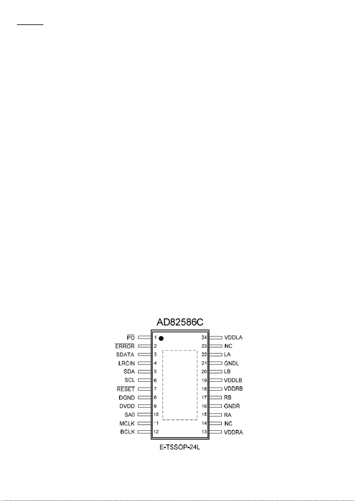
Figure 3.4: Pin description
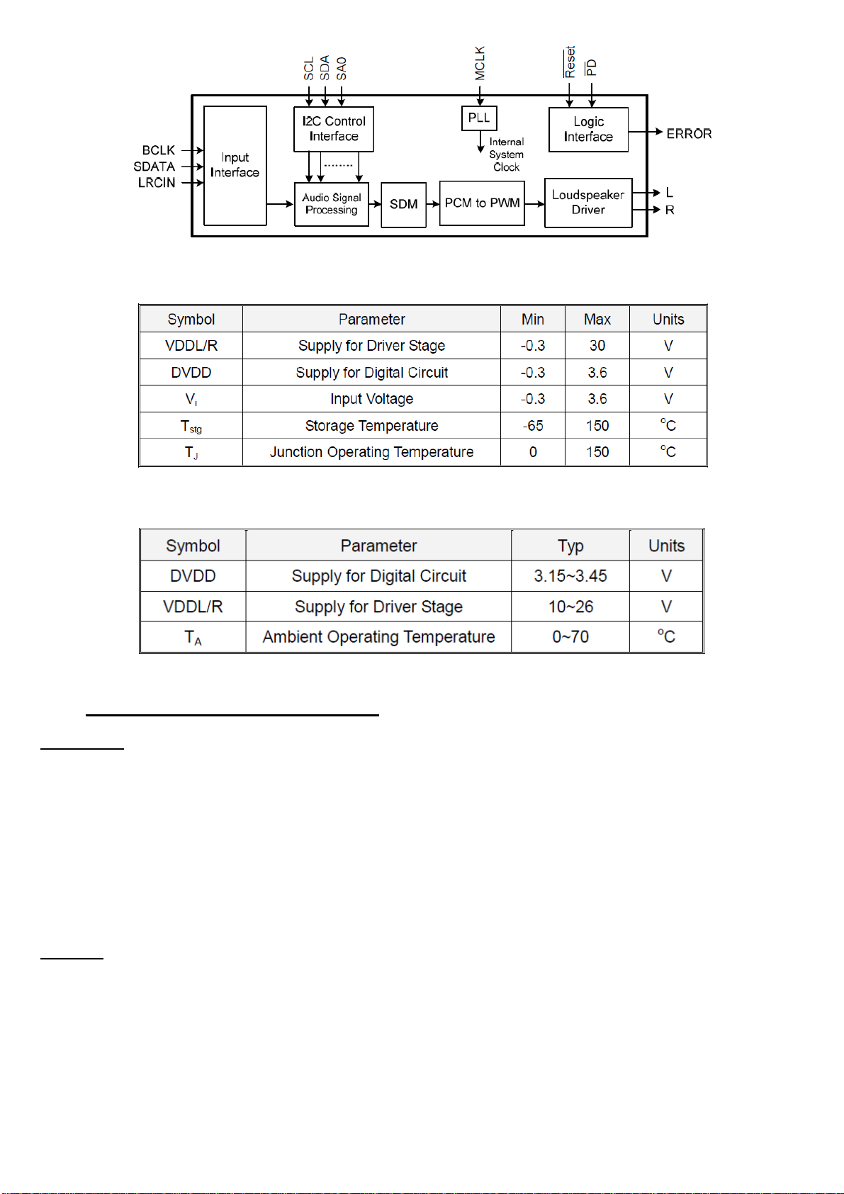
Figure 3.5: Functional Block Diagram
Table 3.3: Absolute Maximum Ratings
Table 3.4: Recommended Operating Conditions
C. HEADPHONE AMPLIFIER (U59)
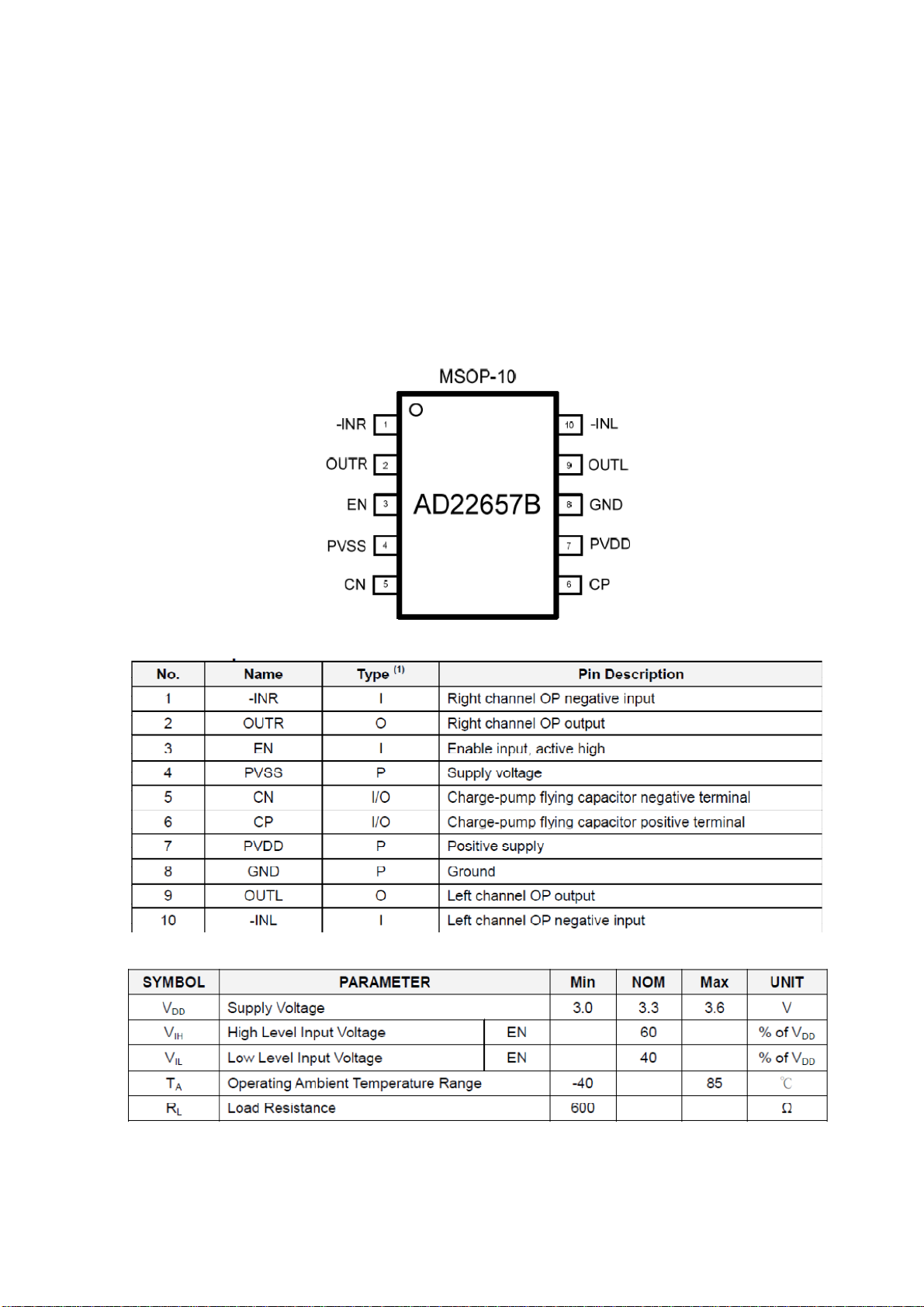
Description
The AD22657B is a 2-Vrms cap-less stereo line driver. The device is ideal for single supply electronics.
Cap-less design can eliminate output dc-blocking capacitors for better low frequency response and save cost.
The AD22657B is capable of delivering 2-Vrms output into a 10k ohm load with 3.3V supply. The gain
settings can be set by users from 1V/V to 10V/V externally. The AD22657B has under voltage protection to
prevent POP noise. Build-in shutdown control and de-pop control sequence also help AD22657B to be a popless device.
The AD22657B is available in a 10-pin MSOP package.
Features
Operation Voltage: 3V to 3.6V
Cap-less Output
Eliminates Output Capacitors
Improves Low Frequency Response
Reduces POP/Clicks
Low Noise and THD
10
Typical SNR 107dB
Typical Vn 7uVrms
Typical THD+N < 0.02%
Maximum Output Voltage Swing into 2.5k Load
2Vrms at 3.3V Supply Voltage
Single-ended Input
External Gain Setting from 1V/V to 10V/V
Fast Start-up Time: 0.5ms
Integrated De-Pop Control
External Under Voltage Protection
Thermal Protection
Less External Components Required
+/-8kV IEC ESD Protection at line outputs
Figure 3.6: Pin description
Table 3.5: Pin functions
11
Table3.6: Recommended operating conditions
D. SUBWOOFER PREAMPLIFIER (U30)
AD22657B is used for subwoofer out, as well.
E. SCART AUDIO AMPLIFIER (U31)
AD22657B is used for scart audio amplifier, as well.
4. POWER STAGE
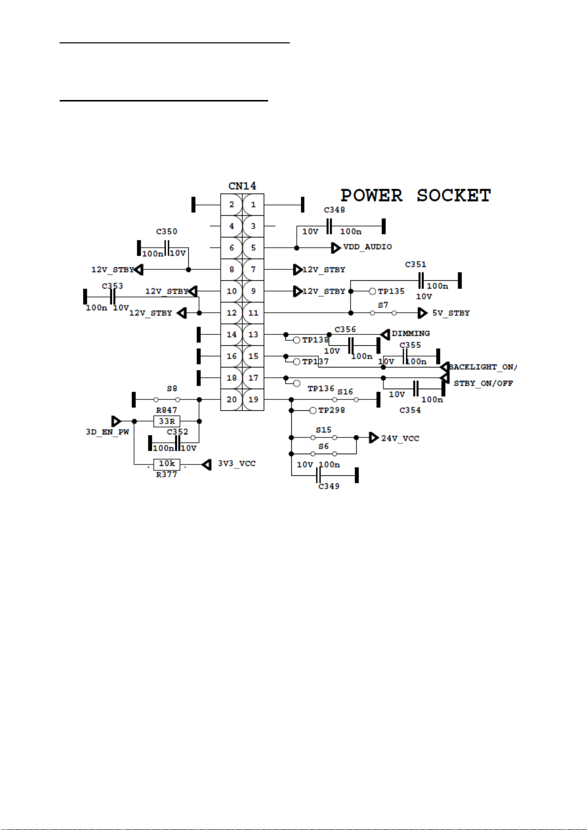
Figure 4.1: Power socket and options.
Power socket is used for taking voltages which are 12V, 5V and VDD_Audio. These voltages are produced
in power board. Also socket is used for giving dimming, backlight and standby signals with power board. It is
shown at figure 4.1.
12

Figure 4.2: General illustration of voltage stages on main board.
VDD_Audio goes directly to the audio side, through power socket other incoming voltages from power card
are converted several voltages, shown in figure 8.
List of the components are:
TPS54528
TPS54628
TPS54821
FDS4685
NTGS3446
APL5910
LM1117
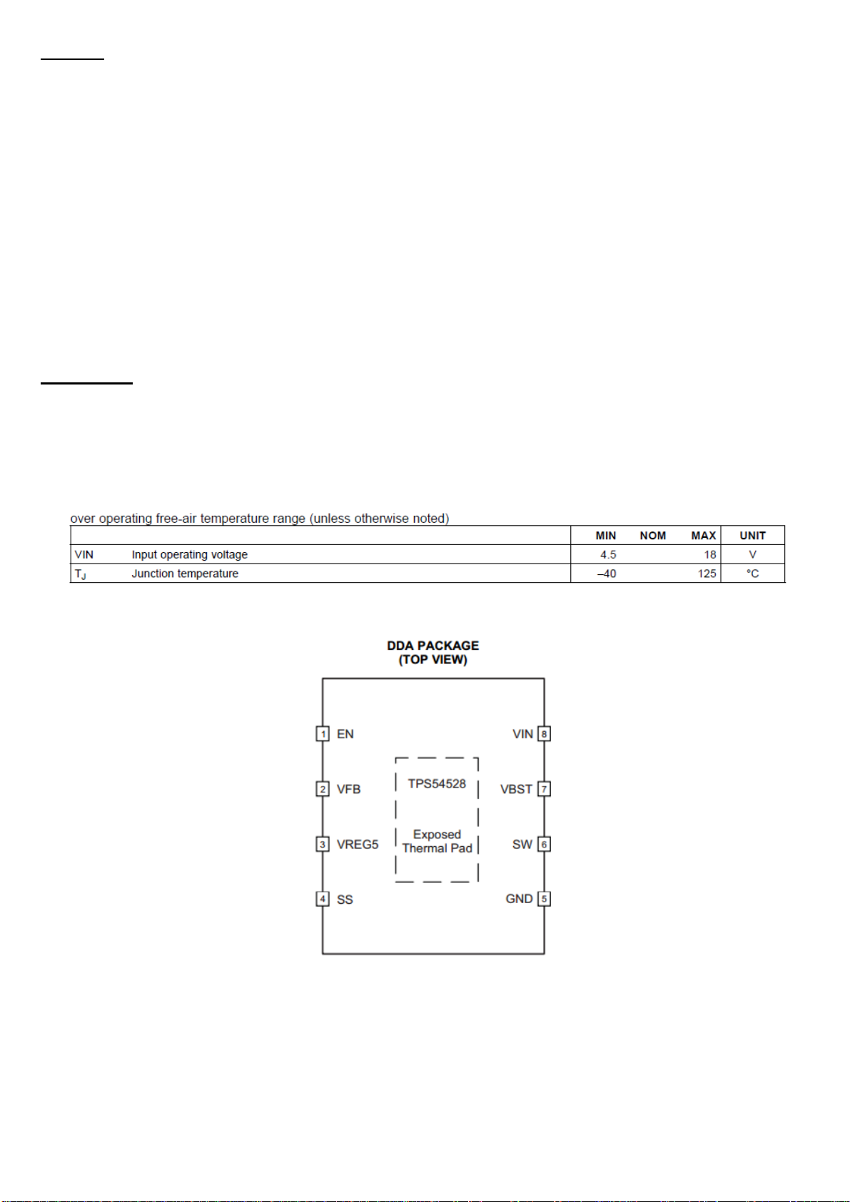
A. TPS54528
General Description
The TPS54528 is an adaptive on-time D-CAP2 mode synchronous buck converter.The TPS54528 enables
system designers to complete the suite of various end-equipment power bus regulators with a cost effective, low
component count, low standby current solution. The main control loop for the TPS54528 uses the D-CAP2
mode control that provides a fast transient response with no external compensation components. The adaptive
on-time control supports seamless transition between PWM mode at higher load conditions and Eco-mode
operation at light loads. Eco-mode allows the TSP54528 to maintain high efficiency during lighter load
conditions. The TPS54528 also has a proprietary circuit that enables the device to adopt to both low equivalent
series resistance (ESR)output capacitors, such as POSCAP or SP-CAP, and ultra-low ESR ceramic capacitors.
The device operates from 4.5-V to 18-V VIN input. The output voltage can be programmed between 0.76 V
and 6 V. The device also features an adjustable soft start time. The TPS54528 is available in the 8-pin DDA
package, and designed to operate from -40 C to 85 C.
13
Features
D-CAP2 Mode Enables Fast Transient Response
Low Output ripple and Allows Ceramic Output Capacitor
Wide V
Input Voltage Range: 4.5 V to 18 V
IN
Output Voltage Range: 0.76 V to 6 V
Highly Efficient Integrated FETs Optimized for Lower Duty Cycle Applications- 65 mOhm (High Side)
and 36 mOhm (Low Side)
High Efficiency, less than 10 mikroAmper at shutdown
High Initial Bandgap Reference Accuracy
Adjustable Soft Start
Pre-Biased Soft Start
650-kHz Switching Frequency (f
SW
)
Cycle By Cycle Over Current Limit
Auto-Skip Eco-mode for High Efficiency at Light Load
Applications
Wide Range of Applications for Low Voltage System
Digital TV Power Supply
High Definition Blu-ray Disc Players
Networking Home Terminal
Digital Set Top Box(STB)
Table 4.1: Recommended operating conditions
Figure 4.3: Pin Description
14
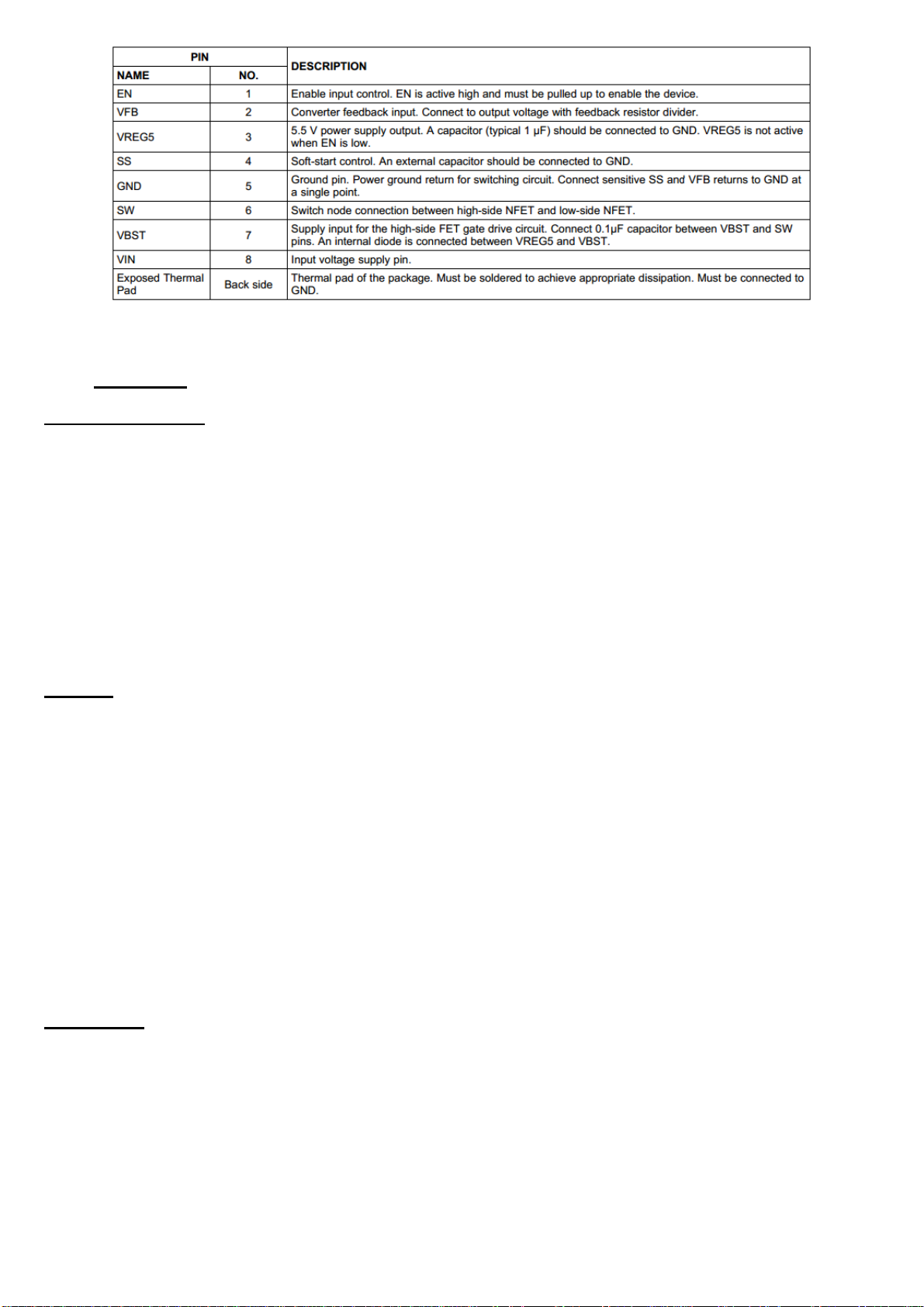
Table 4.2: Pin functions.
B. TPS54628
General Description
The TPS54628 is an adaptive on-time D-CAP2 mode synchronous buck converter.The TPS54628 enables
system designers to complete the suite of various end-equipment power bus regulators with a cost effective, low
component count, low standby current solution. The main control loop for the TPS54628 uses the D-CAP2
mode control that provides a fast transient response with no external compensation components. The adaptive
on-time control supports seamless transition between PWM mode at higher load conditions and Eco-mode
operation at light loads. Eco-mode allows the TSP54628 to maintain high efficiency during lighter load
conditions. The TPS54628 also has a proprietary circuit that enables the device to adopt to both low equivalent
series resistance (ESR)output capacitors, such as POSCAP or SP-CAP, and ultra-low ESR ceramic capacitors.
The device operates from 4.5-V to 18-V VIN input. The output voltage can be programmed between 0.76 V
and 7 V. The device also features an adjustable soft start time. The TPS54628 is available in the 8-pin DDA and
10-pin DRC packages, and is designed to operate over the ambient temperature range of -40C to 85C.
Features
D-CAP2 Mode Enables Fast Transient Response
Low Output ripple and Allows Ceramic Output Capacitor
Wide V
Output Voltage Range: 0.76 V to 7 V
Highly Efficient Integrated FETs Optimized for Lower Duty Cycle Applications- 36 mOhm (High Side)
and 28 mOhm (Low Side)
High Efficiency, less than 10 µA at shutdown
High Initial Bandgap Reference Accuracy
Adjustable Soft Start
Pre-Biased Soft Start
650-kHz Switching Frequency (f
Cycle By Cycle Over Current Limit
Auto-Skip Eco-mode for High Efficiency at Light Load
Input Voltage Range: 4.5 V to 18 V
IN
)
SW
Applications
Wide Range of Applications for Low Voltage System
Digital TV Power Supply
High Definition Blu-ray Disc Players
Networking Home Terminal
Digital Set Top Box(STB)
15
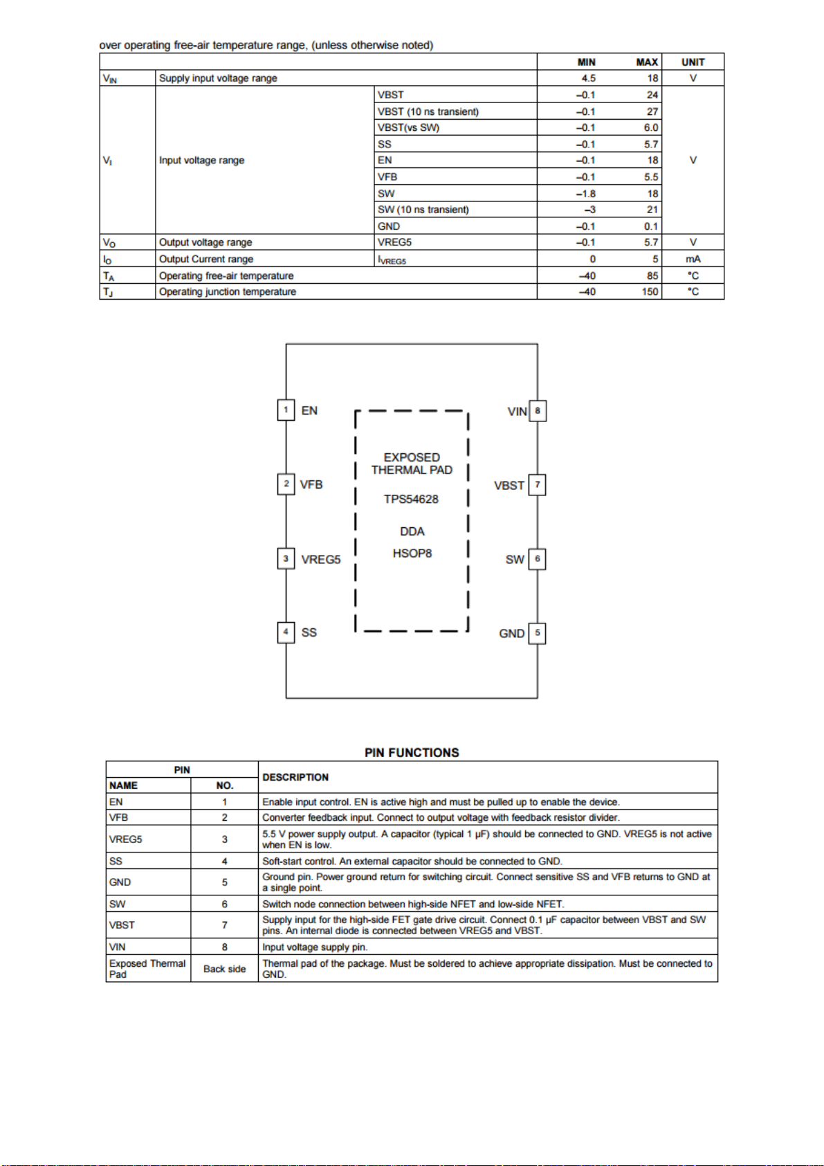
Table 4.3: Recommended operating conditions
Figure 4.4: Pin Description
16
Table 4.4: Pin functions.

C. TPS54821
General Description
The TPS54821 in thermally enhanced 3.5 mm x 3.5 mm QFN package is a full featured 17 V, 8 A
synchronous step down converter which is optimized for small designs through high efficiency and integrating
the high-side and low-side MOSFETs. Further space savings are achieved through current mode control, which
reduces component count, and by selecting a high switching frequency, reducing the inductor's footprint. The
output voltage startup ramp is controlled by the SS/TR pin which allows operation as either a stand alone power
supply or in tracking situations. Power sequencing is also possible by correctly configuring the enable and the
open drain power good pins. Cycle by cycle current limiting on the high-side FET protects the device in
overload situations and is enhanced by a low-side sourcing current limit which prevents current runaway. There
is also a low-side sinking current limit which turns off the low-side MOSFET to prevent excessive reverse
current. Hiccup protection will be triggered if the overcurrent condition has persisted for longer than the preset
time. Thermal hiccup protection disables the device when the die temperature exceeds the thermal shutdown
temperature and enables the part again after the built-in thermal shutdown hiccup time.
Features
Integrated 26 mΩ / 19 mΩ MOSFETs
Split Power Rail: 1.6 V to 17 V on PVIN
200 kHz to 1.6 MHz Switching Frequency
Synchronizes to External Clock
0.6V ±1% Voltage Reference Over Temperature
Low 2 μA Shutdown Quiescent Current
Monotonic Start-Up into Pre-biased Outputs
–40°C to 125°C Operating Junction Temperature Range
Adjustable Input Undervoltage Lockout
Adjustable Slow Start/Power Sequencing
Power Good Output Monitor for Undervoltage and Overvoltage
Adjustable Input Undervoltage Lockout
Applications
Digital TV Power Supplies
Set Top Boxes
Blu-ray DVDs
Home Terminals
17

Table 4.5: Recommended operating conditions
Figure 4.5: Pin Description
18

Table 4.6: Pin functions.
D. FDS4685
General Description
This P-Channel MOSFET is a rugged gate version of Fairchild Semiconductor’s advanced PowerTrench
process. It has been optimized for power management applications requiring a wide range of gate drive voltage
ratings (4.5V – 20V).
Features
–8.2 A, –40 V R
R
DS(ON)
Fast switching speed
High performance trench technology for extremely lowRDS(ON)
High power and current handling capability
= 0.027 @ VGS = –10 V
DS(ON)
= 0.035 @ V
= –4.5 V
GS
19
Figure 4.6: Pins
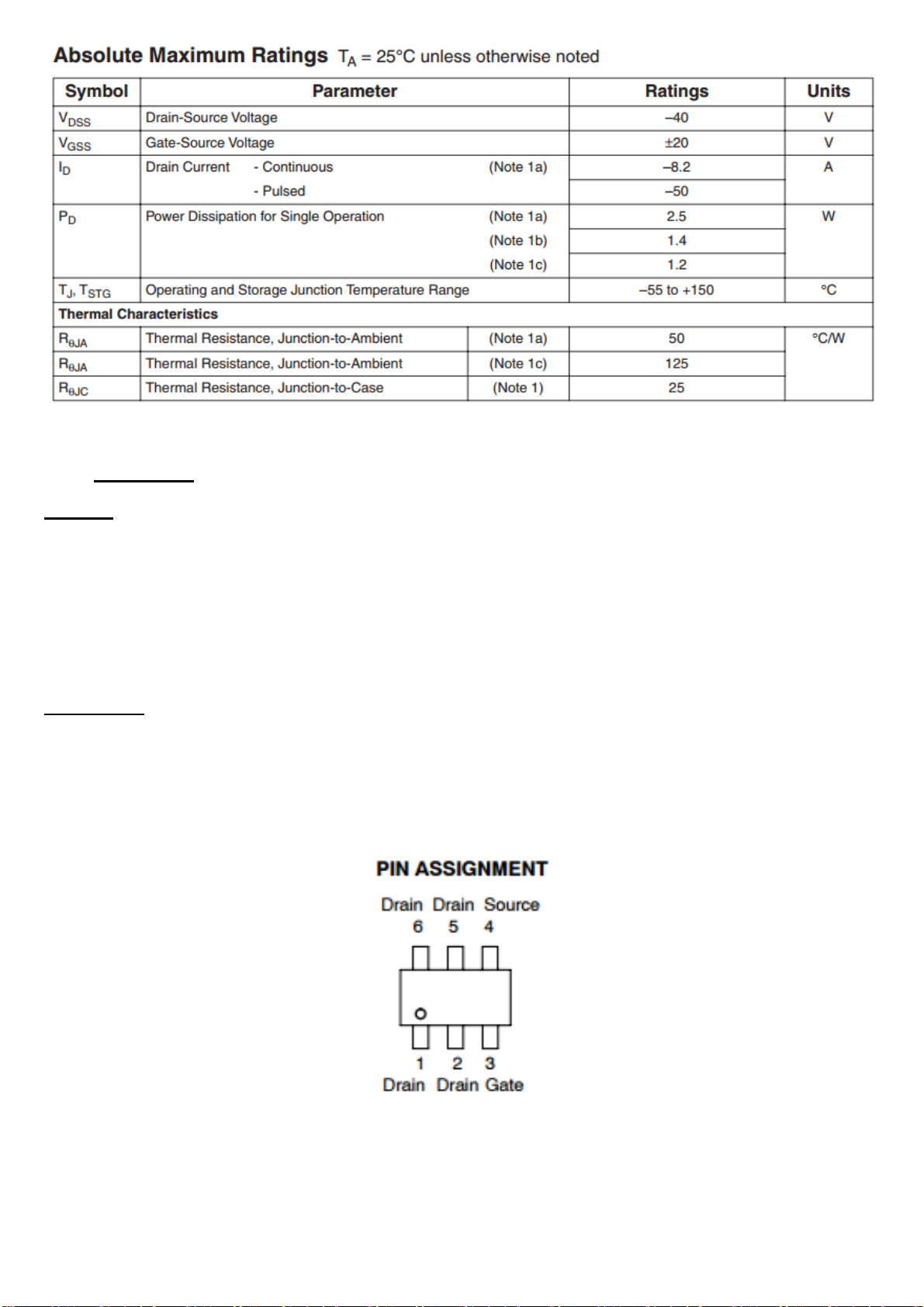
Table 4.7: Absolute maximum ratings
E. NTGS3446
Features
Ultra Low R
Higher Efficiency Extending Battery Life
Logic Level Gate Drive
Diode Exhibits High Speed, Soft Recovery
Avalanche Energy Specified
IDSS Specified at Elevated Temperature
PbFree Package is Available
Applications
Power Management in portable and batterypowered products, i.e. computers, printers, PCMCIA cards,
cellular and cordless
Lithium Ion Battery Applications
Notebook PC
DS(on)
20
Figure 4.7: Pin description
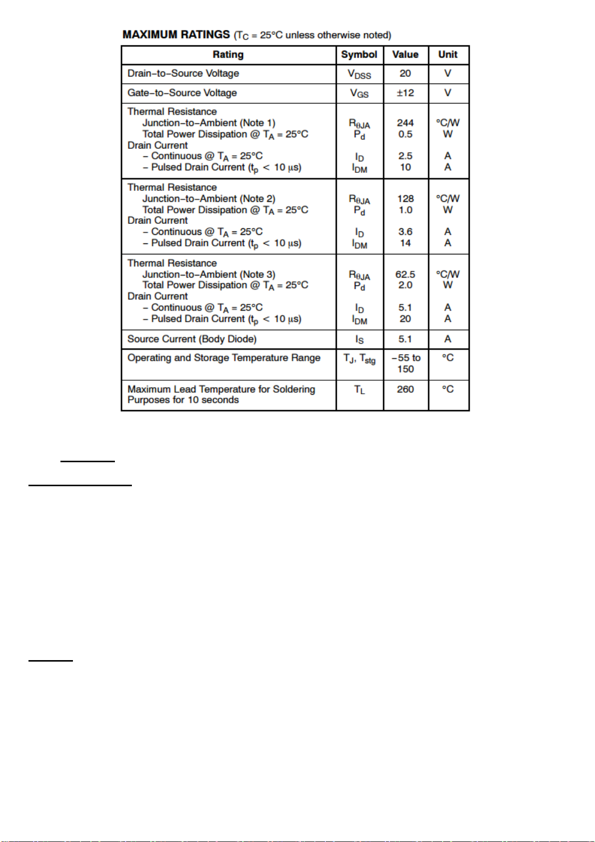
Table 4.8: Maximum ratings
F. APL5910
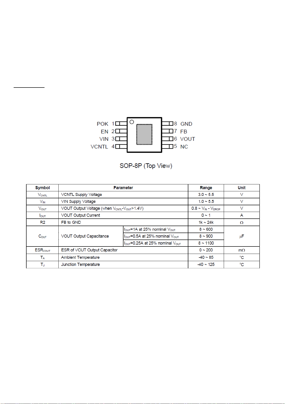
General Description
The APL5910 is a 1A ultra low dropout linear regulator. The IC needs two supply voltages, one is a control
voltage (VCNTL) for the control circuitry, the other is a main supply voltage (VIN) for power conversion, to
reduce power dissipation and provide extremely low dropout voltage. The APL5910 integrates many functions.
A Power-On- Reset (POR) circuit monitors both supply voltages on VCNTL and VIN pins to prevent erroneous
operations. The functions of thermal shutdown and current-limit protect the device against thermal and current
over-loads. A POK indicates that the output voltage status with a delay time set internally. It can control other
converter for power sequence. The APL5910 can be enabled by other power systems. Pulling and holding the
EN voltage below 0.4V shuts off the output.
The APL5910 is available in a SOP-8P package which features small size as SOP-8 and an Exposed Pad to
reduce the junction-to-case resistance to extend power range of applications.
Features
Ultra Low Dropout
- 0.12V (Typical) at 1AOutput Current
0.8V Reference Voltage
High Output Accuracy
- ±1.5%over Line, Load, and Temperature Range
Fast Transient Response
Adjustable Output Voltage
Power-On-Reset Monitoring on Both VCNTL and VIN Pins
21
Internal Soft-Start
Current-Limit and ShortCurrent-Limit Protections
Thermal Shutdown with Hysteresis
Open-Drain VOUT Voltage Indicator (POK)
Low Shutdown Quiescent Current (< 30mA )
Shutdown/Enable Control Function
Simple SOP-8P Package with Exposed Pad
Lead Free and Green Devices Available (RoHS Compliant)
Applications
Motherboards, VGA Cards
Notebook PCs
Add-in Cards
Figure: Pin configuration.
Table 4.9: Recommended operating conditions.
22
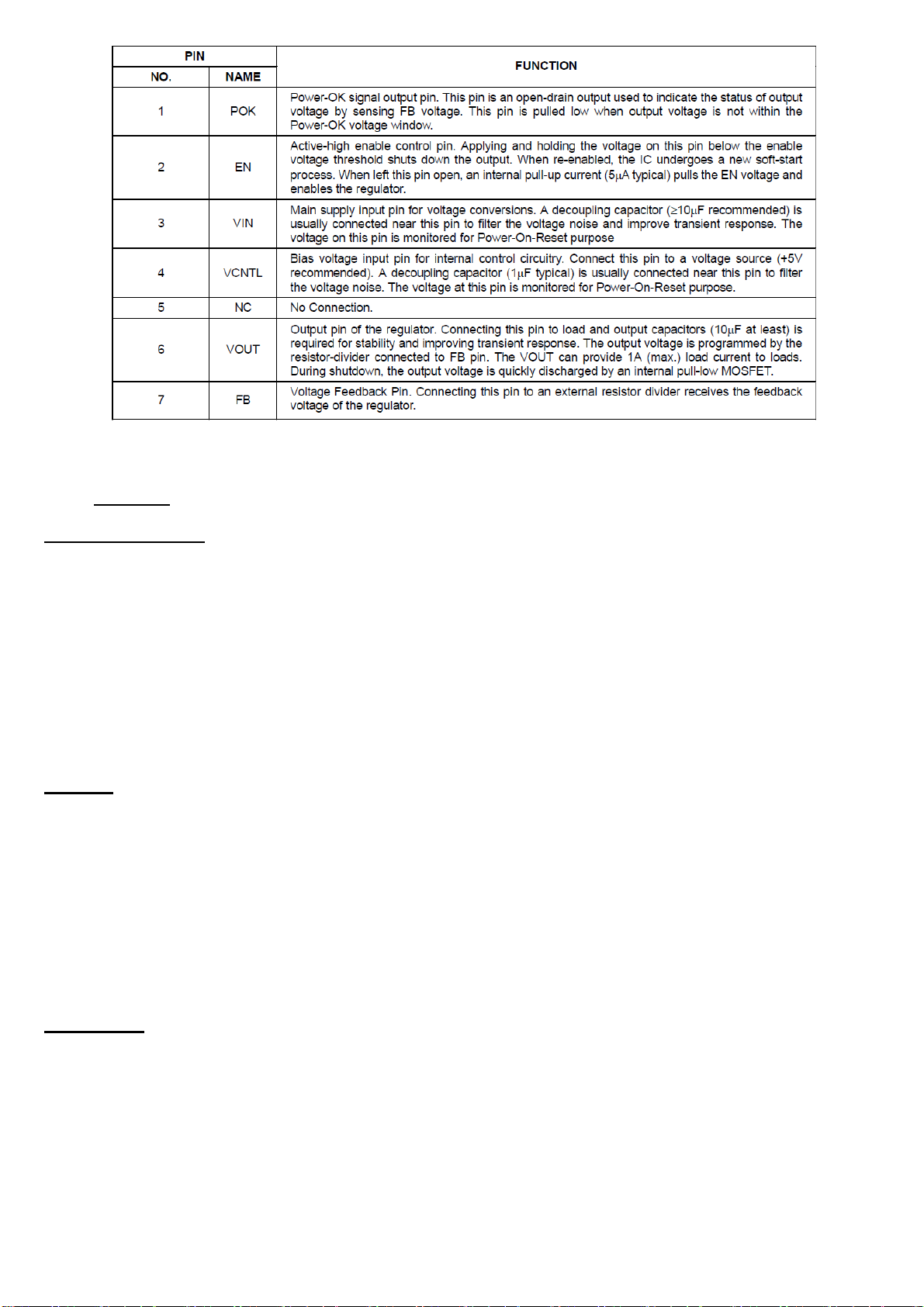
Table 4.10: Pin description.
G. LM1117
General Description
The LM1117 is a series of low dropout voltage regulators with a dropout of 1.2V at 800mA of load current.
It has the same pin-out as National Semiconductor’s industry standard LM317.
The LM1117 is available in an adjustable version, which can set the output voltage from 1.25V to 13.8V
with only two external resistors. In addition, it is also available in five fixed voltages, 1.8V, 2.5V, 2.85V, 3.3V,
and 5V.
The LM1117 offers current limiting and thermal shutdown. Its circuit includes a zener trimmed bandgap
reference to assure output voltage accuracy to within ±1%.
The LM1117 series is available in LLP, TO-263, SOT-223, TO-220, and TO-252 D-PAK packages. A
minimum of 10µF tantalum capacitor is required at the output to improve the transient response and stability.
Features
Available in 1.8V, 2.5V, 2.85V, 3.3V, 5V, and Adjustable Versions
Space Saving SOT-223 and LLP Packages
Current Limiting and Thermal Protection
Output Current 800mA
Line Regulation 0.2% (Max)
Load Regulation 0.4% (Max)
Temperature Range:
- LM1117 0˚C to 125˚C
- LM1117I 40˚C to 125˚C
Applications
2.85V Model for SCSI-2 Active Termination
Post Regulator for Switching DC/DC Converter
High Efficiency Linear Regulators
Battery Charger
Battery Powered Instrumentation
23
 Loading...