

YK
No.020E
42PD8800TA(PW3)
SERVICE MANUAL
32LD8800TA(PW3L)
LCD PDP
Caution
Be sure to read this manual before servicing. To assure safety from fi re, electric shock, injury, harmful radiation and materials, various measures are provided in this HITACHI display.
Be sure to read cautionary items described in the manual to maintain safety before servicing.
Service Warning
1. Since Panel Module and front Filter are made of glass, handling the broken Module and Filter shall be
taken care suffi ciently in order not to be injured.
2. Replacing work shall be started after the Panel Module and the AC/DC Power supply become suffi ciently
cool.
3. Special care shall be taken to the display area in order not to damage its surface.
4. The Panel Module shall not be touched with bare hand to protect its surface from stains.
5. It is recommended to use clean soft gloves during the replacing work in order to protect not only the display area of the Panel Module but also a serviceman himself.
6. The Chip Tube of Panel Module (located upper left of the back and surrounded by frame) and fl exible
cables connecting Panel glasses to drive circuit PWBs are very weak, so shall be taken care suffi ciently
not to break. If you break Chip Tube, the Panel doesn’t display anything forever.
Contents
1. Features --------------------------------------------------3
2. Specifi cations --------------------------------------------4
3. Service point --------------------------------------------- 5
4. Component names ------------------------------------- 6
5. New adoption technology -----------------------------7
6. Adjustment --------------------------------------------- 11
7. Troubleshooting --------------------------------------- 38
8. Self-diagnosis function ------------------------------ 53
SPECIFICATIONS AND PARTS ARE SUBJECT TO CHANGE FOR IMPROVEMENT.
9. Basic circuit diagram --------------------------------- 55
10. Printed wiring board diagram ---------------------- 82
11. Block diagram ----------------------------------------- 90
12. Connection diagram --------------------------------- 91
13. Wiring diagram ---------------------------------------- 93
14. Disassembly diagram -------------------------------- 97
15. Replacement parts list ----------------------------- 101
Plasma Display
November 2005 Digital Media Division

42PD8800/32LD8800
CAUTION FOR SAFETY
Please read this page before repair the monitor.
This page explains to following items for keep the safety of set and prevent to accident during
repair work.
We explain by symbol at happen the damage or injury when took wrong repair.
Warning
Caution
We made the symbol as below, which are kind of following items.
This symbol means "CAUTION"
This symbol means "POSSIBLE to
ELECTRIC SHOCK"
This symbol means "possible to die or heavy damage"
This symbol means "possible to damage or something will break"
This symbol means "MUST"
This symbol means "DO NOT"
WARNING
Should be follows to instructions.
We indicates to cabinet, chassis and parts
by label, which are special attention part.
Please follow to note and [Safety Instructions]
of User’s Manual.
Prevent the electric shock.
Please take care during working because
monitor has high voltage part and power
supply part.
Possible to die if you tough to these place
by miss take.
Please disconnect power plug during
overhaul, reassemble or change parts.
You will die or take damage by electric
shock if you touch to live part.
Use recommended components.
Please use to same characteristic compo-
nent, which is same as previous for your
safety and keep reliability especially marked
by
in parts list and circuit diagram.
It is reason of electric shock or fire if you
use non-recommended component.
Should be kept same style of wiring or component.
Monitor uses tubes or tapes, which made
by insulator, and some components are
keep distance from surface of PWB for
safety.
Internal leads kept from hot part or high voltage
part by clamper or styling, so please return to
original condition for prevent to electric shock
or fire.
Should be done safety check after finished.
Every part (removed screws, component
and wiring) should be returned to previous
condition.
Check around repair position for make
damage by miss take and measure the
insulated impedance by meg-ohm meter.
Confirm the value of impedance, that
value is more than 4M ohm.
It is reason for electric shock or fire if that
value is less than 4M ohm.
Nobody can check and repair to the code
and combination circuit of HDCP.
Never remove the shield case, which is
assembled to the code and combination
circuit of HDCP.
2

42PD8800/32LD8800
PRECAUTIONS
How to clean the plasma screen panel of the monitor
Before cleaning the monitor, turn off the monitor and disconnect the power plug from the power outlet.
To prevent scratching or damaging the plasma screen face, do not knock or rub the surface with sharp or hard
objects. Clean the screen with a soft cloth moistened with warm water and dry with a soft cloth. If it is not
enough, then use a cloth with mild detergent. Do not use harsh or abrasive cleaners.
How to clean the cabinet of the monitor
Use a soft cloth to clean the cabinet and control panel of the monitor. When excessively soiled dilute a neutral
detergent in water, wet and wring out the soft cloth and afterward wipe with a dry soft cloth.
Never use acid/alkaline detergent, alcoholic detergent, abrasive cleaner, powder soap, OA cleaner, car wax,
glass cleaner, etc. especially because they would cause discoloration, scratches or cracks.
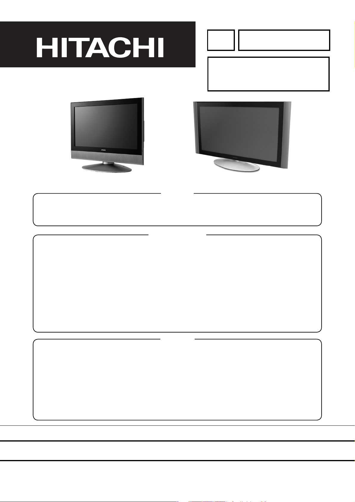
1. Features
Large-screen, high-definition plasma display panel
The 42-inch color plasma display panel, with a resolution of 1024 (H) x 1024 (V) pixels, and the 32-inch color LCD
panel with a resolution of 1366(H) x 768(V) pixels, creates a high-definition, large-screen(aspect ratio : 16:9) and lowprofile flat display. Free from electromagnetic interferences from geomagnetic sources and ambient power lines, the
panel produces high-quality display images free from color misconvergence and display distortion.
High Performance Digital Processor
A wide range of input signals can be handed,including composite, component,and HDMI.High Definition Digital Processor creates the fine-textured image with dynamic contrast. In addition, it corresponds to a broad array of personal computer signals, from 640 x 400 and 640 x 480 VGA to 1600 x 1200 UXGA.(RGB Input)
Easy-to-use remote control and on screen display system
The remote control included eases the work of setting display controls. Further, the on-screen display system,
displays the status of signal reception and display control settings in an easy-to-view fashion.
Power saving system
The power saver feature saves power consumption automatically when input signals are not available.
When connected to a VESA DPMS-compliant PC, the monitor cuts its power consumption while it is idle.
Connecting to an Audio Visual Device
• Two composite/S terminal*
a photo input terminal have been added. A composite video output terminal is also provided as a
monitoring output.
*1
One composite/S terminal are on the side input. Composite terminal and S terminal should not be con-
nected at the same time
*2
Two composite terminal and two component terminal cannot be used at the same time.
• A wide range of devices other than personal computers can also be connected.
Power Swivel Feature
It allows to turn the display left or right within ± 30 degree using the remote control.
1
,three composite terminal*2, two component terminal*2, two HDMI terminal and
3
42PD8800/32LD8800
2. Specifications
Approx. 32 inches
(698(H) x 392(V)mm, diagonal 801mm)
Panel
Display dimensions
Resolution 1366(H) x 768(V) pixels 1024(H) x 1024(V) pixels
including Stand :
Net dimensions
813(W) x 663(H) x 350(D)mm
excluding Stand :
813(W) x 584(H) x 114(D)mm
Net weight
Ambient
conditions
Temperature Operating : 5°C to 35°C, Storage : 0°C to 40°C
Relative humidity Operating : 20% to 80%, Storage : 20% to 90% (non-condensing)
including Stand : 27.6kg
excluding Stand : 21.9kg
Power supply AC100 - 240V, 50/60Hz
Power consumption / at standby
150W / <1W(100 - 220V)
150W / <1.1W(230 - 240V)
Audio output speaker total 20W speaker total 36W
(VIDEO input)
AV1•2 : composite video input terminal (RCA) or component video input terminal (RCA)
L/R audio input terminal (RCA)
AV3•5 : composite video input terminal (RCA) or S video input terminal.
L/R audio input terminal (RCA)
Input terminals
AV4 : composite video input terminal (RCA)
L/R audio input terminal(RCA)
HDMI1•2 : HDMI input terminal
Audio input terminal (3.5mm Stereo Mini Jack)
Photo Input : Photo Input terminal / SD card slot
Input signals
Composite video : PAL, SECAM, NTSC3.58, NTSC4.43, PAL60
Component video : 480i, 576i, 480p, 576p, 720p/50, 720p/60, 1080i/50, 1080i/60
OUTPUT (MONITOR) : composite video monitor-output terminal (RCA)
Output Signal
OUTPUT (MONITOR) : L/R audio monitor-output terminal (RCA)
OUTPUT (HEADPHONE) : L/R audio monitor-output terminal (Mini-pin)
OUTPUT (SUB-WOOFER) : Woofer output terminal
(RF input)
Input terminals ANT : 75Ω Unbalanced
PAL B, G, H / I / D, K
RF Video System
SECAM B, G / D, K / K1
NTSC-M
(RGB input)
Input terminals
Analog RGB input terminal (D-sub 15-pin)
Audio unput terminal (3.5mm Stereo Mini Jack)
Input signals 0.7V/1.0Vp-p, analog RGB (Recommended Signal)
H/V separate, TTL level [2KΩ]
Sync signals
H/V composite, TTL level [2KΩ]
Sync on green, 0.3Vp-p [75Ω]
•The monitor takes at least 30 minutes to attain the status of optimal picture quality.
Approx. 42 inches
(922(H) x 522(V)mm, diagonal 1059mm)
including Opional Stand :
1134(W) x 728(H) x 350(D)mm
excluding Optional Stand :
1134(W) x 648(H) x 98(D)mm
including Opional Stand : 43.0kg
excluding Opional Stand : 37.3kg
370W / <3W
Applicable video signals for each input terminal
Terminal RCA D-sub
Signal CVBS S-video Component RGB RGB
AV1,2
AV3
AV4
AV5 *
HDMI1,2
RGB
Note : CVBS and S-video on AV5 should not be connected
at the same time to prevent interference on the picture
4
HDMI
( :Available)
42PD8800/32LD8800
3. Service points
Lead free solder
This product uses lead free solder (unleaded) to help preserve the environment. Please read these instructions
before attempting any soldering work.
Caution: Always wear safety glasses to prevent fumes or molten solder from getting into the eyes. Lead free
solder can splatter at high temperatures (600˚C).
Lead free solder indicator
Printed circuit boards using lead free solder are engraved with an "F."
Properties of lead free solder
The melting point of lead free solder is 40-50˚C higher than leaded solder.
Servicing solder
Solder with an alloy composition of Sn-3.0Ag-0.5Cu or Sn-0.7Cu is recommended.
Although servicing with leaded solder is possible, there are a few precautions that have to be taken. (Not taking
these precautions may cause the solder to not harden properly, and lead to consequent malfunctions.)
Precautions when using leaded solder
Remove all lead free solder from soldered joints when replacing components.
If leaded solder should be added to existing lead free joints, mix in the leaded solder thoroughly after the lead
free solder has been completely melted (do not apply the soldering iron without solder).
Servicing soldering iron
A soldering iron with a temperature setting capability (temperature control function) is recommended.
The melting point of lead free solder is higher than leaded solder. Use a soldering iron that maintains a high
stable temperature (large heat capacity), and that allows temperature adjustment according to the part being
serviced, to avoid poor servicing performance.
Recommended soldering iron:
Soldering iron with temperature control function (temperature range: 320-450˚C)
Recommended temperature range per part:
Part Soldering iron temperature
Mounting (chips) on mounted PCB 320˚C±30˚C
Mounting (chips) on empty PCB 380˚C±30˚C
Chassis, metallic shield, etc. 420˚C±30˚C
The PWB assembly which has used lead free solder
SUBPOWER PWB (Subpower PWB, Filter PWB, Terminal PWB)
SOUND PWB (Audio PWB, Control PWB, SW PWB)
FC PWB
MAIN PWB (Main PWB, LED PDP PWB, LED LCD PWB, Swivel PWB)
Readjustment Power supply voltage (PDP only)
When a PANEL or a Power Unit is exchanged, power supply voltage needs to be adjusted. Please adjust to
make the values of Va and Vs of as should on the label currently stuck on the panel back upper parts.Adjustment is performed by VR in the power supply unit. Please refer to the procedures of “Va” and “Vs” adjustments
on 22page.
5
4. Component names
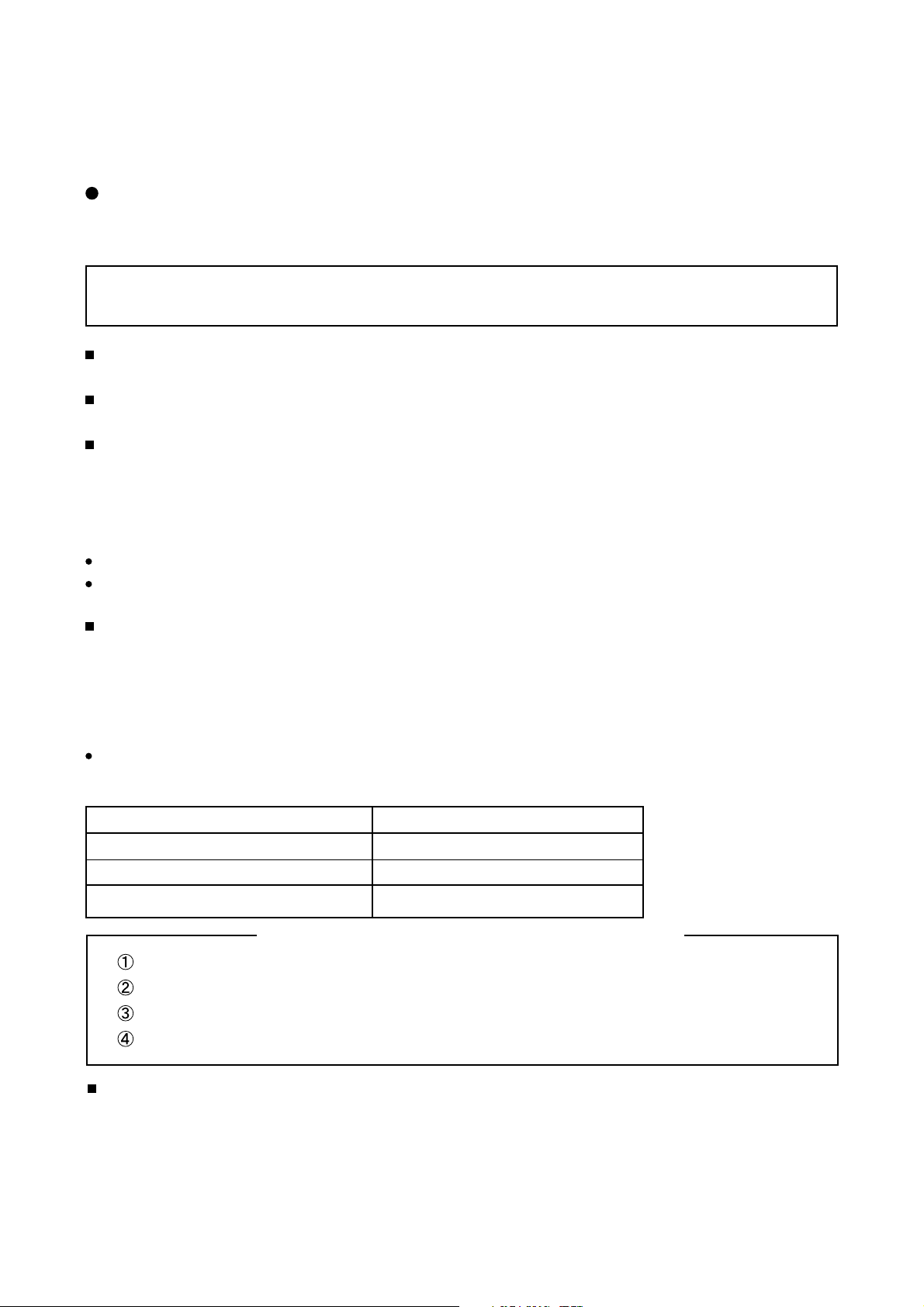
[Main unit]
Control panel
42PD8800/32LD8800
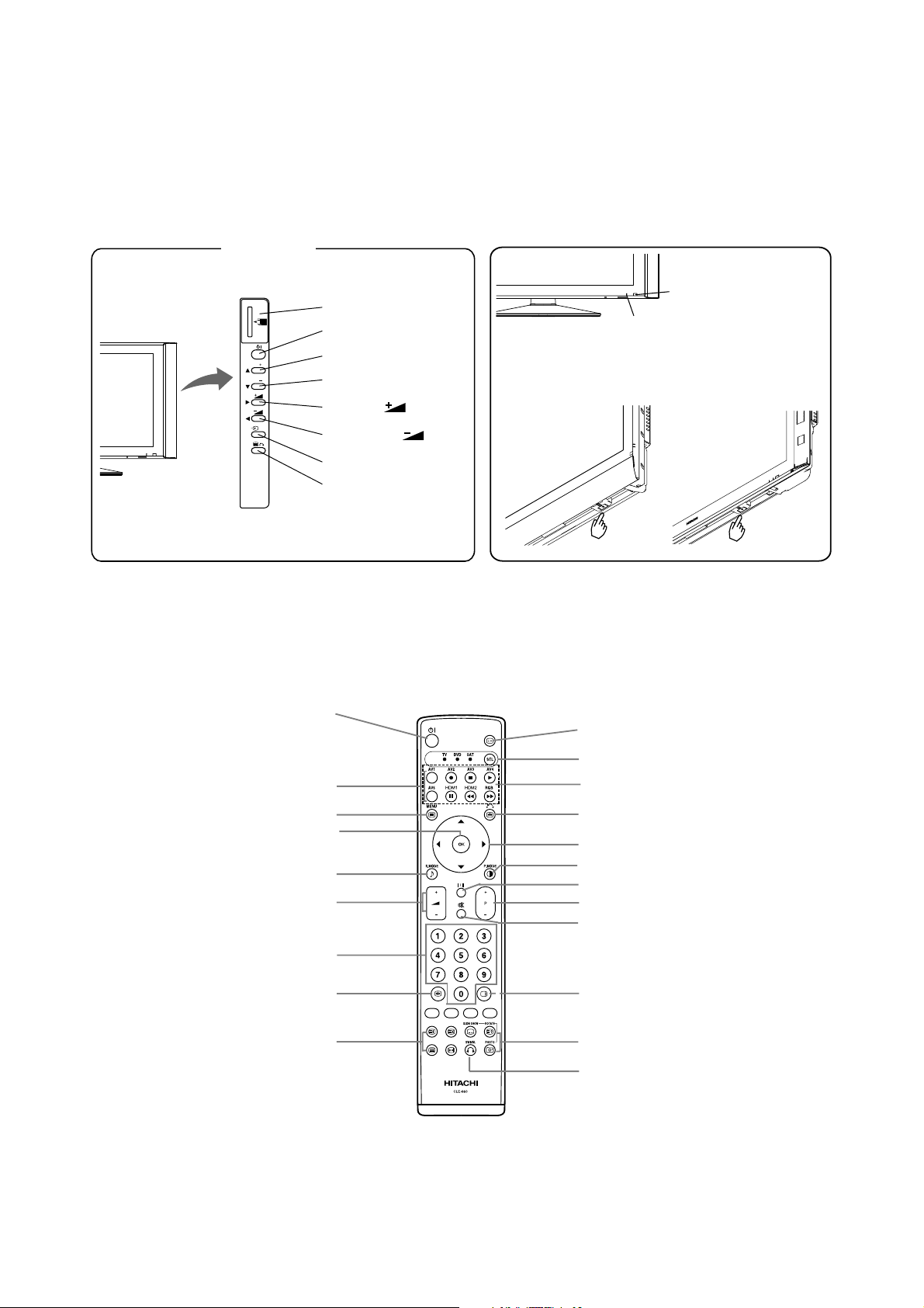
[Remote control]
SD MEMORY
CARD
PUSH-EJECT
P
P
OK
PH35814
POWER button
SD Memory Card Slot
Sub Power button
Channel UP/▲button
Channel DOWN/▼button
Volume UP
Volume DOWN
Input Select /OK button
Menu / Return button
/►button
/◄button
Remote Control
Receiver
Indicating Lamp
• The main power switch is located on the lower surface.
Main power switch
(32")
(42")
RECALL button
INPUT SELECT buttons
MENU button
OK button
SOUND MODE button
VOLUME UP/DOWN button
PROGRAM SELECT buttons
(TV)
FREEZE/MULTI MODE button
T/TEXT button
(TV)
FUNCTION SELECT button
DVD CONTROL buttons
RETURN button
SELECT/ADJUST button
PICTURE MODE button
CH I/CH II button (TV)
CHANNEL UP/DOWN button (TV)
MUTE button
MULTI PICTURE button
PHOTO INPUT buttons
SWIVEL button
CLE-970
6

42PD8800/32LD8800
5. New adoption technology
[System control micom I001(M30627)]
Pin function table
No. PIN NAME I/O
VREF (+5.0V) I PDP/ LCD 5V
1
2
3
4
5
6
7
8 DATA_OUT(FC)
9 DATA_IN(FC)
10 CLK(FC)
11
12
13
14
15
16
17
18
19
20
21
22
23
24
25
26
27
28
29
30
31
32
33
34
35
36
37
38
39
40
41
42
43
44
45
46
47
48
49
50
+5.0V I PDP/ LCD 5V
AUDIO_SW1 I/O PDP/ LCD Audio SW1
OSD_DATA I/O PDP/ LCD OSD DATA
OSD_CLK I/O PDP/ LCD OSD CLK
HP_VOL
FUNC_1 I/O PDP/ LCD
BL_INST I/O PDP/ LCD Black Insert On/Off for 32V LCD (37V=Low)
BL_BLINK I/O PDP/ LCD Backlight Blink On/Off for 32V LCD (37V=Low)
GND I PDP/ LCD GND
CNVSS(FLASH) I PDP/ LCD CNVSS(FLASH)
DSUB COMP I/O PDP/ LCD Sync Switching
RGBSW I/O PDP/ LCD Sync Switching
RESET I PDP/ LCD Reset
16MHz Oscillation O PDP/ LCD OSC-OUT
GND I PDP/ LCD GND
16MHz Oscillation I PDP/ LCD OSC-IN
+5.0V I PDP/ LCD 5V
NMI(+5.0V) I PDP/ LCD 5V PULL UP
RMCON I/O PDP/ LCD Receiving Remote Control Signal
NC I/O PDP/ LCD NC
V.FREQ_3 I/O PDP/ LCD V.Frequency
SCV.SYNC I/O PDP/ LCD SUB_Y.SYNC (Composite䋩
IRQ䋨PM-IRQ) I/O PDP/ LCD PDP Control
MCV.SYNC I/O PDP/ LCD MAIN_Y.SYNC (Composite䋩
POWER_LED I/O PDP/ LCD L䋺Lighting (Power Save)
FUNC_2 I/O PDP/ LCD Function2
CEC_OUT I/O PDP/ LCD CEC OUT(CEC1)
H.FREQ_3 I/O PDP/ LCD H.Frequency
PDWN
RXD2 I/O PDP/ LCD RS-232C Communication
TXD2 I/O PDP/ LCD RS-232C Communication
TXD1(RS232C/FLASH) I/O PDP/ LCD FLASH for Writing
RXD1(RS232C/FLASH) I/O PDP/ LCD FLASH for Writing
SCLK(FLASH) I/O PDP/ LCD FLASH for Writing
BUSY(FLASH) I/O PDP/ LCD FLASH for Writing
TXD0(DTT) I/O PDP/ LCD DTT
RXD0(DTT) I/O PDP/ LCD DTT
SDA4(panel) I/O PDP/ LCD PDP Communication䋨I2C Bus䋩
SCL4(panel) I/O PDP/ LCD PDP Communication䋨I2C Bus䋩
M_ENABLE I/O PDP/ LCD Media Enable
M_SCLK I/O PDP/ LCD
M_SDA I/O PDP/ LCD
M_WAKEUP I/O PDP/ LCD Media Wakeup
PDPGO(PM_ON) I/O PDP/ LCD PDP Control/LCD Panel 12V/WVGA Power
Panel: PDP/ LCD
I/O PDP/ LCD Head Phone Volume
I/O PDP/ LCD FC MicroComputer 3 Lines Bus Data Out /Media Data Out
I/O PDP/ LCD FC MicroComputer 3 Lines Bus Data In/ Media Data In
I/O PDP/ LCD FC MicroComputer 3 Lines Bus Clock/ Media Clock
I/O PDP/ LCD
I PDP/ LCD 5V
I PDP/ LCD GND
FUNCTION
Panel LVDS
Media Clock
Media Data
Function1
7
42PD8800/32LD8800
No. PIN NAME I/O
CPUGO(PM_CPU) I/O PDP/ LCD PDP Control/Inverter Voltage
51
EPM (FLASH) I/O PDP/ LCD FLASH for Writing
52
VIDEO.DET_1 I/O PDP/ LCD
53
54
55
56
57
58
59
60
61
62
63
64
65
66
67
68
69
70
71
72
73
74
75
76
77
78
79
80
81
82
83
PDP_WVGA_LCD_SW_ I/O PDP/42WVGA/LCD Detection
84
85
86
87
88
89
90
91
92
93
94
95
PDP_WVGA_LCD_SW_ I/O PDP/ LCD PDP/42WVGA/LCDᬌ
96
97
98
99
100
SCL1 I/O PDP/ LCD
SDA1 I/O PDP/ LCD
HDMI-RESET I/O PDP/ LCD
HDMI-HPD_RESET I/O PDP/ LCD
SEL_0 I/O PDP/ LCD FC Clock/Others SW
SEL_1 I/O PDP/ LCD HDMI/DTT SW
TUNER.DET_1 I/O PDP/ LCD TUNER Detection
CE (FLASH) I/O PDP/ LCD FLASH for Writing
STAND.CIR_DET I/O PDP/ LCD Stand Detection
SW_L_OUT I/O PDP/ LCD
SW_R_OUT I/O PDP/ LCD
M_SW I/O PDP/ LCD Bridge Media Circuit Connection Judgement Terminal
INITIALIZE I/O PDP/ LCD Memory Initial
BR_MUTE I/O PDP/ LCD Bridge Media Audio Mute
CK_SEL I/O PDP/ LCD Clock Selector
SCDT I/O PDP/ LCD HDMI Power Save for Return
CK_INV I/O PDP/ LCD Clock Invert
DVI-SW I/O PDP/ LCD DVI Control
CUR_PRTCT I/O PDP/ LCD Power Swivel Overcurrent Detection
SP_MUTE I/O PDP/ LCD SP Relay
AUDIO_MUTE I/O PDP/ LCD Audio MUTE
ASEL1 I/O PDP/ LCD Audio Switching SW
ASEL2 I/O PDP/ LCD Audio Switching SW
SDA2 I/O PDP/ LCD I2C(TAS3103/TAS5508)
SCL2 I/O PDP/ LCD I2C(TAS3103/TAS5508)
D-SUB I/O PDP/ LCD
BM_SW I/O BM Switching
RGB_BLK_2 I/O NC
RGB_BLK_3 I/O NC
AUDIO_RESET I/O Audio Circuit Reset
+5.0V I
EDID_PROTECT_1 I/O PDP/ LCD Memory Protect(Not necessary if power is available to use䋩
GND I PDP/ LCD GND
WSS_1 I/O PDP/ LCD NC
WSS_2 I/O PDP/ LCD NC
WSS_3 I/O PDP/ LCD NC
TV.AFC(M) I/O PDP/ LCD Main Tuner Control (AFC)
TV.AFC(S) I/O PDP/ LCD Sub Tuner Control (AFC)
AUDIO_SW2 I/O PDP/ LCD Audio SW2
EDID_PROTECT_2 I/O PDP/ LCD Memory Protect(Not necessary if power is available to use䋩
HP_DETECT I/O PDP/ LCD HEAD PHONE DETECT
INT_HDMI I/O PDP/ LCD
CEC_IN I/O PDP/ LCD CEC IN(CEC2)
COMP_SW I/O PDP/ LCD Component SW Main 㹤 DSUB
DEMP_OUT I/O PDP/ LCD
Panel: PDP/ LCD
I2C䋨To the Side of Main Board䋩 FE/MSP3455or MSP3415G/SAA5361
I2C䋨To the Side of Main Board䋩 FE/MSP3455or MSP3415G/SAA5361
D-SUB COMP for Sync Switching
De-emphasis Control Output for HDMI
FUNCTION
VIDEO Board Detection
HDMI-Reset
Hot Plug Detect Reset
Swivel L Output
Swivel R Output
INT(HDMI)
8
42PD8800/32LD8800
No. PIN NAME I/O
101
102
103
104
105
106
107
108
109
110
111
112 IRQ_DTT
113 DTT_POWER
114 DISPEN
115
116
117
118 SCL6
119 SDA6
120 COLOR_SYS
121
122
123
124
125
126
127
128
NC I/O LCD NC
SCL0 I/O PDP/ LCD
SDA0 I/O PDP/ LCD
SCL3(EEPROM) I/O PDP/ LCD
SDA3(EEPROM) I/O PDP/ LCD
EPGGO I/O PDP/ LCD EPGGO
EXT_RESET I/O PDP/ LCD EXTERNAL RESET
OSD_CS I/O PDP/ LCD OSD CS
FC_ENABLE I/O PDP/ LCD FC MicroComputer 3 Lines Enable
V_P_DET_1 I/O PDP/ LCD V_DET_1(Power Save Return䋩
V_P_DET_2 I/O PDP/ LCD V_DET_2(Power Save Return䋩
HDMI_A_SW I/O PDP/ LCD HDMI AUDIO SW
SCL5 I/O PDP/ LCD
SDA5 I/O PDP/ LCD
AD_KEY3 I/O PDP/ LCD AD KEY3**
AD_KEY2 I/O PDP/ LCD AD KEY2*
AD_KEY1 I/O PDP/ LCD AD KEY1(Power)
TV.POWER I/O PDP/ LCD H:PowerON䇮L:(Standby,PowerSave)
DIP.DET I/O PDP/ LCD DIP DET
POWER_SAVE I/O PDP/ LCD L䋺Lighting(Standby䍂PowerSave), H䋺Lights-out
GND I PDP/ LCD GND
FAN_ALARM *1 I/O PDP/ LCD FAN ALARM
Panel: PDP/ LCD
2
I
C䋨To the Side of Main Board䋩 (TA1391FG/CXA2069/uPD64015/TB1274AF)
2
I
C䋨To the Side of Main Board䋩 (TA1391FG/CXA2069/uPD64015/TB1274AF)
I/O PDP/ LCD DTT IRQ
I/O PDP/ LCD DTT POWER
I/O PDP/ LCD DISPEN/Backlight on
I/O PDP/ LCD I2C䋨To the Side of Sensor Board䋩 (AD7414䋩
I/O PDP/ LCD I2C䋨To the Side of Sensor Board䋩 (AD7414䋩
I/O PDP/ LCD Color System (Pull-in range Switching䋩
FUNCTION
2
I
C䋨EEPROM䋩
2
I
C䋨EEPROM䋩
2
I
C䋨Sil9021䋩
2
I
C䋨Sil9021䋩
9

R
(M3062
)
T
E
SW
V
K
PROTECT
1
RESET
䇼
A0/A1h
T
)
R
IRQ)
WVGA
LCD
SW1
(TB12
4)
414
*1/V0
A31FTV *2/ENG29
**G *3)
A
T
CPU)
6
P130
HPD
RESET
䇽
6Ah
䇽
)
T
W
X
R
FREQ
3
2239 )
(CXA2069Q)
G*
MSP34
G *4)
08
䋩
KEY3
4
DET
AV1
䇼
36h
䇽
A
A
PROTECT
2
AN2
3
3
AFC(M)
SOUT4
90/91h
䇽
3D
Y/C
A
SW
P13
ENABLE
(
PD6401
)
2
A
ALARM
P134
WAKEUP
361
TV
SEL
4
WVGA PANEL
P124
SW
䇼
䇽
TV
SEL
1
2
P123
BLK
2
TV
SEL
2
SCL4
DET
(TA1391FG)
FE
SW
2
SCL0
AGC
30/31h
DETECT
䇽
L
DTT
P113
P112
SCL4
T
C
SW
TXD1
TXD_RXD
䇼
0
l
0V
V
Buffer
Buffer
Block diagram
42PD8800/32LD8800
LCD PANE
SDA4
PDP
WVGA
32LCD
PANEL TYPE
P17
00
01
10
䌐120
*3䇼84/85h䇽
SDA1 SDA2
55
UDIO PROCESSO
SDA2
SCL2
55
5
RESET MSP_RESET
5
SOUND MULTIPLE
_
_
-
SDA0 S-2 S_DET_AV3 SDA1
AV S
SCL0 S-1 SCL1
S2-2
FE Sub
-
SCL1
PDP
_
_
_
_
.
.
.
.
FE.SW_1 SDA4 SDA4
5
5
L
u
SDA0 TELETEXT TV.SEL_3
SCL0
SDA0 Text Ys_SW
DA
S_Trap
5
UDIO PROCESSO
SCL2
5
-
TUNER (FE Main)
7
TEMPERATURE
SENSOR (0ption
37LCD11
7
Level
P56
7
MAIN µ-COMPUTE
HP_VOL DA1 P54 VIDEO.DET_1
DSUB COMP P87 P53 SEL_2
RGB SW P86 P52 SEL_1
POWER_SAVE P101 P51 TUNER.DET
POWER_LED P76
M_SCK P136 P127 STAND.CIR_DE
TV.POWER P103 P126 SW_L_OUT
EEPROM
_
7
BR_MUTE P45 P125 SW_L_OUT
CK_SEL P44 P46 INITIALIZ
P42 P47 M_SW
CK_IN
SCL3
DVI-SW P41 P07
_
P140 P06 SDA3
_
_
BL_BLIN
P40 P32
UD RST P121 P115 DISPEN
CUR_PRTC
SP_MUTE P37 P33
UDIO_MUTE P36 P133
SEL1 P35 P132
_
_
_
7
-
SEL2 P34 P11
PDWN P72 P10
V_P_DET_1 P01 VIDEO DECODER
DA0 P120 PDP_WVGA_LCD_SW2 SCL0 P111 SCL6 SCL1
P135 SDA0 P110 SDA6
M_SD
FC SUB µ-com
_
_
5
P84
TA2OUT
_
RMCON(AVC
CEC_OU
PDPGO(PM_ON) P57 P131 HDMI_RESE
_
_
.
10
V_P_DET_2 P00 CLK3 CLOCK
SCV.SYNC TA4IN SOUT3 DATA IN
_
5
N27 WSS_1
N26 WSS_2 OSD CONTROLER S2-3
N5
_
_
_
D_KEY2
UDIO_SW2 P22
MCV.SYNC TA3IN SIN3 DATA OUT S-3 COMP_DET_AV2
N23 CLK4 SCLK S2-4
N4 P03 CS
.
D_KEY1
TV.AFC(S)
_
7
_
_
_
P75 M_SD
_
H.FREQ_3 TA1IN M_SCLK
FUNCTION_
_
_
_
_
_
BL_INST P141 P122 RGB_BLK_3 SYNC SEPARATION
_
7
P13 P65 SCLK(FLASH) SCL5
_
_
_
DTT RXD0 TXD2 RS232C
DTT_POWER P116 P61
DEMP_OU
D-SUB P31
CEC_IN P15 CNVss CE EPM CNVss
5
orma
5
5
COLOR_SYS P107 P55 EPM Flash Writing 5V 0V 5V

42PD8800/32LD8800
6. Adjustment
● How to get to Adjustment mode
Using the front control buttons with the set turned off (standby) can activate it.
Press the SUB-POWER(
more than 5 seconds.
The set turns on in adjustment mode with OSD.
● Changing data and Selecting Adjustment code
When the set is in adjustment mode, the cursor , , , and OK buttons of the remote control or front panel
may be used as the adjustment keys.
, buttons are used for selecting adjustment code.
, buttons are used for changing data values.
OK button is used for confirming the data.
After finishing the necessary adjustment press MENU button. Adjustment mode is released and the set returns to
normal condition.
● Memory Initialize operation
NOTE: The execution of this function returns the adjustment codes to the preset values, therefore, adjustment
data will be lost.
Procedure
(1) Enter Adjustment Mode.
(2) Select MEMORY INIT adjustment code (No.818) and change the data value from 0 to 1.
(3) Activate MEMORY INIT by pressing OK button.
(4) Select No.712 and change data value from 1 to 0.
(5) Check that the receiving channel goes to P1. Unit is set to preset values.
) button, INPUT SELECT( ) button and button at the same time, and hold for
11
42PD8800/32LD8800
Service
Adj.
No
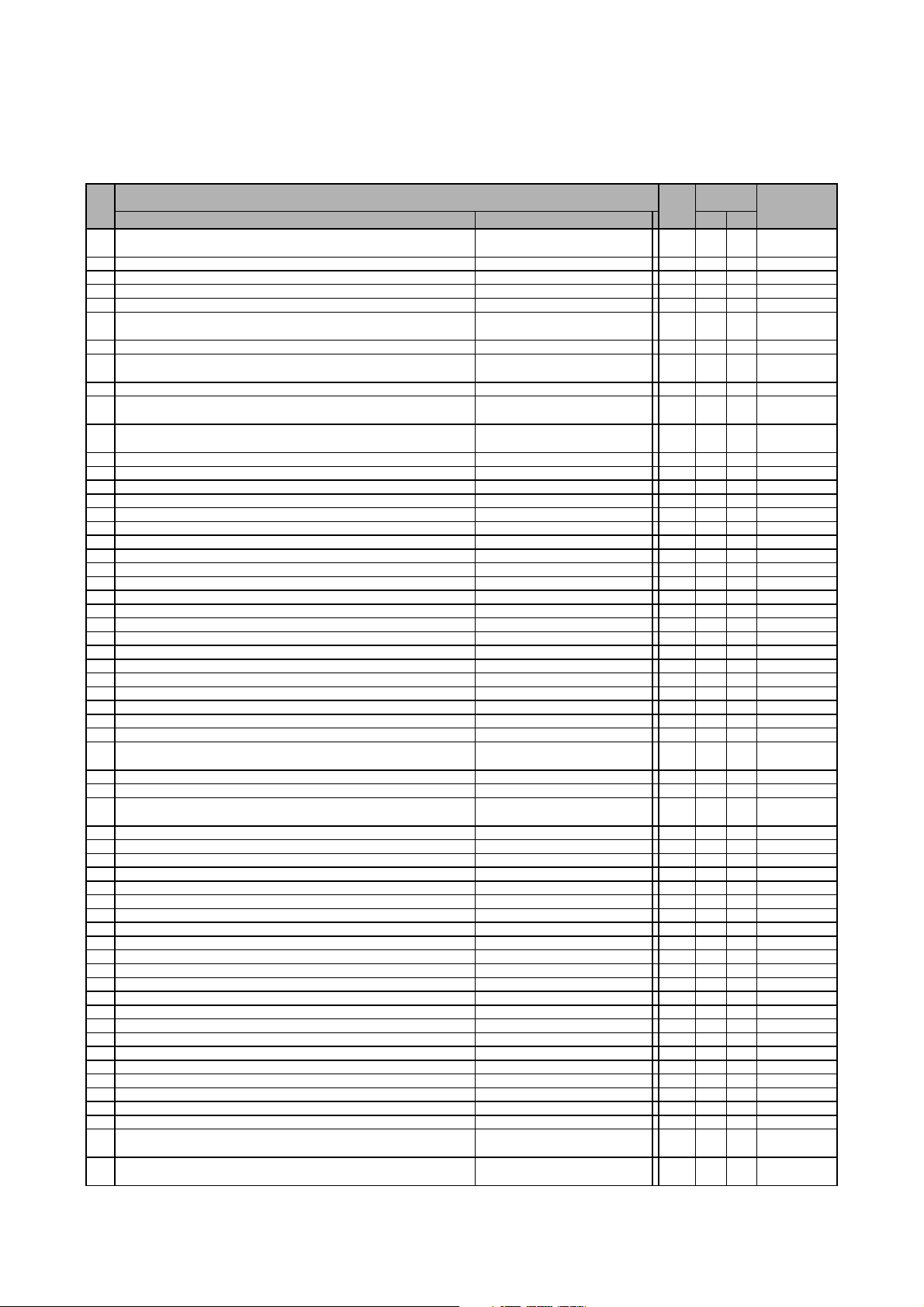
0 SUB_CONTRAST (AV1) Sub Composite mode 15 8 8 TB1274
1 SUB_CONTRAST (AV2) Sub Composite mode 15 8 8 TB1274
2 SUB_CONTRAST (AV3) Sub Composite mode 15 8 8 TB1274
3 SUB_CONTRAST (AV4) Sub Composite mode 15 8 8 TB1274
4 SUB_CONTRAST (AV5) Sub Composite mode 15 8 8 TB1274
5 SUB_CONTRAST (RF) Sub 15 8 8 TB1274
6 Sub Color Sub 15 8 8 TB1274
7 TINT (RF) Sub 63 29 29 TB1274
8 TINT (VIDEO) Sub 63 29 29 TB1274
9 Reference Amplitude(RGB_AMP) RF/VIDEO 254 127 127 FC
10 Reference Amplitude(RGB_AMP) PC 254 127 127 FC
11Reference Amplitude(RGB_AMP) Multi Picture mode 254 130 130 FC
12 Display for Max. Amplitude Level Main - - - FC
13 Display for Max. Amplitude Level Sub - - - FC
14 Set Blue Gamma gain On/Off 0:Off, 1:On (For 55V) For 55V 1 1 1 FC
15 Contrast mode<Dynamic> SW (TV) 0:Dynamic, 1:Dynamic+Auto RF 1 1 1 FC
16 APL Enhancer 0:OFF, 1:ON For Dynamic mode 1 1 1 FC
17 HDMI PC Function 0:OFF, 1:ON (for customer request) 1 0 0
18 PinP Function (for PC) 0:PinP, 1:Infomation1, 2:Infomaiton Split 2 0 0 FC
19 Black Level(RGB_AMP) RF/VIDEO 254 127 127 FC
20 Black Level(RGB_AMP) PC 254 127 127 FC
21 Black Level(RGB_AMP) For USA NTSC/480i 254 127 127 FC
22 Protect for Image Retention 0:Off, 1:7%, 2:14%, 3:21%, 4:AUTO Dynamic mode 4 4 4 FC
23 Protect for Image Retention 0:Off, 1:7%, 2:14%, 3:21%, 4:AUTO Natural mode 4 4 4 FC
24 Protect for Image Retention 0:Off, 1:7%, 2:14%, 3:21%, 4:AUTO Cinema mode 4 4 4 FC
25 YNR Input Level RF 7 7 7 FC
26 YNR Input Level VIDEO 7 7 7 FC
27 YNR Input Level Scart-RGB(50/60Hz) 7 7 7 FC
28 YNR Input Level 480i/576i 7 7 7 FC
29 YNR Input Level 480p/576p 7 7 7 FC
30 YNR Input Level for AV1-5 Mode 1080i-50/60/720p 7 7 7 FC
31 YNR Input Level for →HDMI Mode 480i/480p/576i/576p/VGA 7 7 7 FC
32 YNR Input Level for →HDMI Mode 1080i-50/60/720p 7 7 7 FC
33 CNR Input Level at Low level for AV1-5 Mode RF/VIDEO 7 3 3 FC
34 CNR Input Level at Low level for AV1-5 Mode Scart-RGB(50/60Hz) 7 3 3 FC
35 CNR Input Level at Low level for AV1-5 Mode 480i/576i 7 3 3 FC
36 CNR Input Level at Low level for AV1-5 Mode 480p/576p 7 3 3 FC
37 CNR Input Level at Low level for AV1-5 Mode 1080i-50/60/720p 7 3 3 FC
38 CNR Input Level at Low level for →HDMI Mode 480i/480p/576i/576p/VGA 7 2 2 FC
39 CNR Input Level at Low level for →HDMI Mode 1080i-50/60/720p 7 2 2 FC
40 Main/Sub YFRNR Pass Level [MYNRP0] NTSC/PAL/Multi 7 1 1 FC
41 [MYNRP5] NTSC/PAL-VIDEO 7 0 0 FC
42 [MYNRP6'] Scart-RGB(50/60Hz) 7 0 0 FC
43 [MYNRP6] 480i/576i (Except HDMI) 7 0 0 FC
44 [MYNRP7] 480p/576p (Except HDMI) 7 0 0 FC
45 [MYNRP8] 1080i-50/60/720p (Except HDMI) 7 0 0 FC
46 [MYNRP6] 480i/576i (HDMI) 7 0 0 FC
47 [MYNRP7] 480p/576p (HDMI) 7 0 0 FC
48 [MYNRP8] 1080i-50/720p-50 (HDMI) 7 1 1 FC
49 [MYNRP8'] 1080i-60/720p-60 (HDMI) 7 0 0 FC
50 Main/Sub CFRNR Pass Level [MCNRP0] NTSC/PAL/Multi 7 2 0 FC
51 [MCNRP5] NTSC/PAL-VIDEO 7 2 0 FC
52 [MCNRP6'] Scart-RGB(50/60Hz) 7 2 0 FC
53 [MCNRP6] 480i/576i 7 2 0 FC
54 [MCNRP7] 480p/576p 7 2 0 FC
55 [MCNRP8] 1080i-50/60/720p 7 0 0 FC
56 Vertical Enhancer Gain for B-Y/B, R-Y/R [CVEG0] NTSC/PAL/480i/576i/Multi 15 15 15 FC
57 [CVEG1] 480p/576p/1080i-50/60/720p 15 9 9 FC
58 Vertical DSB Gain for B-Y/B, R-Y/R [CVDSBG0] NTSC/PAL/480i/576i/Multi 3 0 0 FC
59 [CVDSBG1] 480p/576p/1080i-50/60/720p 3 0 0 FC
adjustment items by I
ADJ. Items Mode PDP LCD
2
C-bus control (MAIN Part)
Function
Max.
value
Init. Value
Device
12

42PD8800/32LD8800
Adj.
No
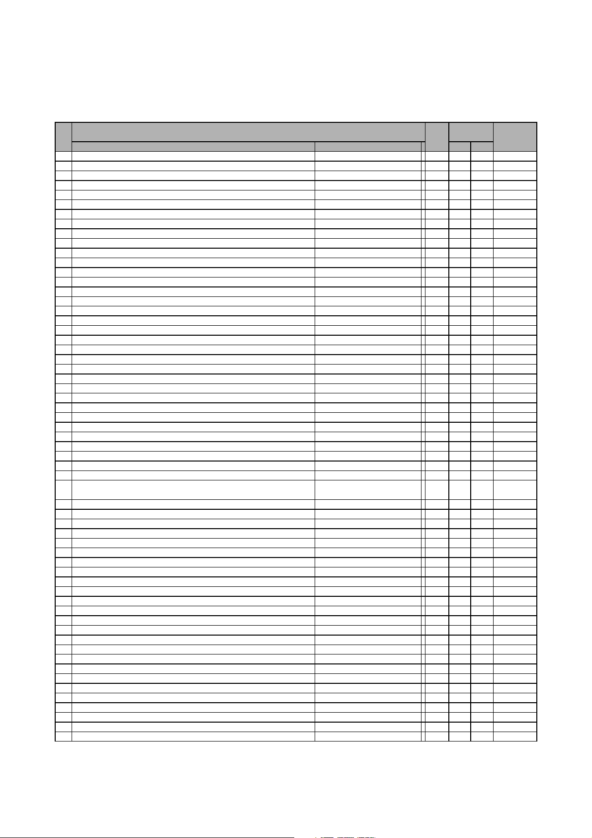
60 Vertical DSB coring for B-Y/B, R-Y/R [CVDSBC0] NTSC/PAL/480i/576i/Multi 7 0 0 FC
61 [CVDSBC1] 480p/576p/1080i-50/60/720p 7 0 0 FC
62 Vertical Enhancer CLIP 0:CTI for B-Y/B, R-Y/R [CVECLP0] NTSC/PAL/480i/576i/Multi 1 0 0 FC
63 [CVECLP1] 480p/576p/1080i-50/60/720p 1 0 0 FC
64 Horizontal HPF Peak Frequency Switch for B-Y/B, R-Y/R [CHHPF0] NTSC/PAL/480i/576i/Multi 3 2 2 FC
65 [CHHPF1] 480p/576p/1080i-50/60/720p 3 2 2 FC
66 Horizontal Enhancer Gain for B-Y/B, R-Y/R [CHEG0] NTSC/PAL/480i/576i/Multi 15 15 15 FC
67 [CHEG1] 480p/576p/1080i-50/60/720p 15 9 9 FC
68 Horizontal DSB Gain for B-Y/B, R-Y/R [CHDSBG0] NTSC/PAL/480i/576i/Multi 3 0 0 FC
69 [CHDSBG1] 480p/576p/1080i-50/60/720p 3 0 0 FC
70 Horizontal DSB Coring for B-Y/B, R-Y/R [CHDSBC0] NTSC/PAL/480i/576i/Multi 7 0 0 FC
71 [CHDSBC1] 480p/576p/1080i-50/60/720p 7 0 0 FC
72 Horizontal Enhancer CLIP 0:CTI for B-Y/B, R-Y/R [CHECLP0] NTSC/PAL/480i/576i/Multi 1 0 0 FC
73 [CHECLP1] 480p/576p/1080i-50/60/720p 1 0 0 FC
74 B-Y Clamp Offset NTSC/PAL/480i/576i/480p/576p 255 128 128 FC
75 R-Y Clamp Offset NTSC/PAL/480i/576i/480p/576p 255 128 128 FC
76 B-Y Clamp Offset 1080i-50/60 255 128 127 FC
77 R-Y Clamp Offset 1080i-50/60 255 128 127 FC
78 B-Y Clamp Offset 720p 255 128 128 FC
79 R-Y Clamp Offset 720p 255 128 128 FC
80 B-Y Clamp Offset [DVI-STB] →[HDMI] 480i/576i/480p/576p/VGA 255 128 128 FC
81 R-Y Clamp Offset [DVI-STB] →[HDMI] 480i/576i/480p/576p/VGA 255 128 128 FC
82 B-Y Clamp Offset [DVI-STB] →[HDMI] 1080i-50/60 255 128 128 FC
83 R-Y Clamp Offset [DVI-STB] →[HDMI] 1080i-50/60 255 128 128 FC
84 B-Y Clamp Offset [DVI-STB] →[HDMI] 720p 255 128 128 FC
85 R-Y Clamp Offset [DVI-STB] →[HDMI] 720p 255 128 128 FC
86 FC6 THROUGH 0:OFF, 1:THROUGH ON 1 0 0 FC
87 Dynamic Back Light Correction For LCD 1 1 1 FC
88 Dynamic Contrast Correction 111 FC
89 Histogram Color Management 111 FC
90 Histogram Gradation Amp. 111 FC
91 Histogram Enhancer 111 FC
92 Dynamic Enhancer 111 FC
93 Main H Sync Phase Adjustment (MHPHS) DTT 255 101 101 FC
94 Sub H Sync Phase Adjustment (SHPHS) DTT 255 101 101 FC
95 P/N ID Sub 1 0 0 TB1274
96 Sharpness Gain(RF/NR) Sub 15 2 2 TB1274
97 Sharpness Gain(RF) BG/DK/I Sub 15 8 8 TB1274
98 Sharpness Gain(RF) M Sub 15 8 8 TB1274
99 Sharpness Gain(RF) L Sub 15 8 8 TB1274
100 Sharpness Gain(RF) L' Sub 15 8 8 TB1274
101 Sharpness Gain(VIDEO) PAL Sub 15 8 10 TB1274
102 Sharpness Gain(VIDEO) NTSC3.58 Sub 15 8 10 TB1274
103 Sharpness Gain(VIDEO) SECAM,B/W Sub 15 8 10 TB1274
104 Sharpness Gain(VIDEO) NTSC4.43 Sub 15 8 10 TB1274
105 Sharpness Gain(VIDEO) N-PAL Sub 15 8 10 TB1274
106 Sharpness Gain(VIDEO) M-PAL Sub 15 8 10 TB1274
107 Sharpness Gain(S.VIDEO) Sub 15 10 8 TB1274
108 Sharpness f0(RF) BG/DK/I Sub 3 2 2 TB1274
109 Sharpness f0(RF) M Sub 3 2 2 TB1274
110Sharpness f0(RF) L Sub 3 2 2 TB1274
111Sharpness f0(RF) L' Sub 3 2 2 TB1274
112Sharpness f0(VIDEO) PAL Sub 3 2 2 TB1274
113Sharpness f0(VIDEO) NTSC3.58 Sub 3 2 2 TB1274
114Sharpness f0(VIDEO) SECAM,B/W Sub 3 2 2 TB1274
115Sharpness f0(VIDEO) NTSC4.43 Sub 3 2 2 TB1274
116Sharpness f0(VIDEO) N-PAL Sub 3 2 2 TB1274
117Sharpness f0(VIDEO) M-PAL Sub 3 2 2 TB1274
118Y Out Level M (4.5) Sub 63 19 15 TB1274
119Y Out Level B/G (5.5) Sub 63 13 13 TB1274
ADJ. Items Mode PDP LCD
Function
Max.
value
Init. Value
Device
13

42PD8800/32LD8800
Adj.
No
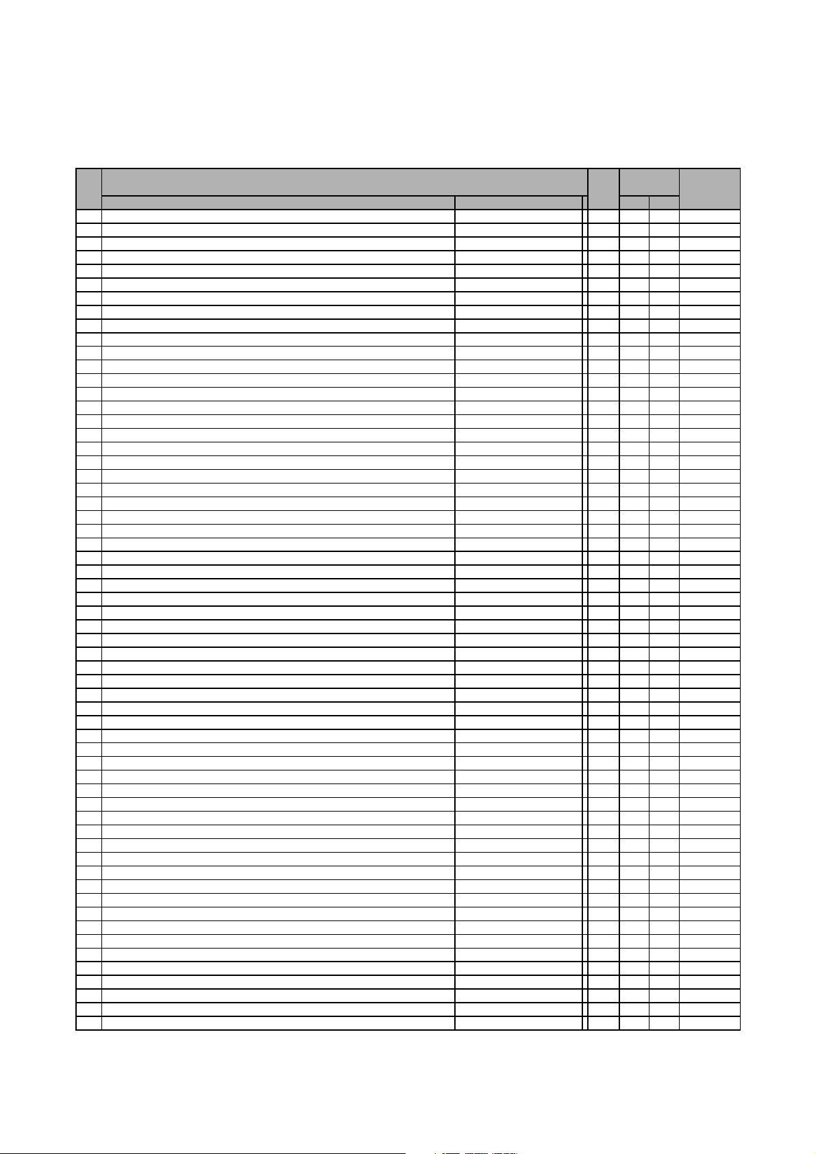
120 Y Out Level D/K (6.5) Sub 63 12 12 TB1274
121 Y Out Level I (6.0) Sub 63 13 13 TB1274
122 Y Out Level L (6.5) Sub 63 12 12 TB1274
123 Y Out Level L' (6.5) Sub 63 15 15 TB1274
124 Y Out Level (VIDEO) Sub 63 13 13 TB1274
125 Y Out Level (TEXT) Sub 63 4 4 TB1274
126 C Out Level M (4.5) Sub 63 3 12 TB1274
127 C Out Level B/G (5.5) Sub 63 8 8 TB1274
128 C Out Level D/K (6.5) Sub 63 8 8 TB1274
129 C Out Level I (6.0) Sub 63 7 7 TB1274
130 C Out Level L (6.5) Sub 63 7 7 TB1274
131 C Out Level L' (6.5) Sub 63 7 7 TB1274
132 C Out Level (VIDEO) Sub 63 10 10 TB1274
133 C Out Level (TEXT) Sub 63 8 8 TB1274
134 BPF_Q (4.43MHz) Sub 3 3 3 TB1274
135 BPF_f0 (4.43MHz) Sub 3 1 1 TB1274
136 C_TRAP_SW (COMB=OFF-PAL/NTSC4.43/NTSC3.58) Sub 1 0 0 TB1274
137 LPF Sub 1 0 0 TB1274
138 SECAM D-Trap Sub 1 1 1 TB1274
139 FILTER SW(RF) Sub 1 0 0 TB1274
140 Y_DL (4.5MHz) Sub 10 5 5 TB1274
141 Y_DL (5.5MHz PAL/NTSC4.43) Sub 10 2 2 TB1274
142 Y_DL (5.5MHz SECAM) Sub 10 0 0 TB1274
143 Y_DL (6.0PAL/NTSC4.43) Sub 10 7 7 TB1274
144 Y_DL (6.0SECAM) Sub 10 5 5 TB1274
145 Y_DL (6.5PAL/NTSC4.43) Sub 10 5 5 TB1274
146 Y_DL (6.5SECAM) Sub 10 5 5 TB1274
147 Y_DL (L) Sub 10 5 5 TB1274
148 Y_DL (L') Sub 10 5 5 TB1274
149 Y_DL (VIDEO PAL/NTSC4.43) Sub 10 5 5 TB1274
150 Y_DL (VIDEO SECAM) Sub 10 5 5 TB1274
151 Y_DL (VIDEO NTSC) Sub 10 5 5 TB1274
152 NTSC Comb(Comb off) Sub 1 1 1 TB1274
153 Cb offset1 Sub 15 8 8 TB1274
154 Cr offset1 Sub 15 8 8 TB1274
155 MVM (VIDEO) 1 0 0 TB1274
156 AFC_GAIN (AV00) 3 0 0 TB1274
157 AFC_GAIN (AV1) 3 0 0 TB1274
158 AFC_GAIN (AV2) 3 0 0 TB1274
159 AFC_GAIN (AV3) 3 0 0 TB1274
160 AFC_GAIN (AV4) 3 0 0 TB1274
161 AFC_GAIN (AV5) 3 0 0 TB1274
162 AFC_GAIN (Except AV00) 3 0 0 TB1274
163 S_B-Y_ADJ Sub 15 8 8 TB1274
164 S_R-Y_ADJ Sub 15 8 8 TB1274
165 BELL_f0 Sub 1 0 0 TB1274
166 S_INHBT 1 0 0 TB1274
167 S_ID 1 0 0 TB1274
168 S_GP 3 0 0 TB1274
169 S_V_ID 1 0 0 TB1274
170 BELL/HPF 3 3 3 TB1274
171 HS Phase Sub 1 0 0 TB1274
172 Bandwidth 1 NTSC/PAL/480i/576i 3 1 1 TA1391FG
173 Bandwidth 1 480p/576p 3 2 2 TA1391FG
174 Bandwidth 1 1080i-50/60/720p 3 0 0 TA1391FG
175 Bandwidth 1 DTT 3 2 2 TA1391FG
176 Bandwidth 2 NTSC/PAL/480i/576i 3 2 2 TA1391FG
177 Bandwidth 2 480p/576p 3 2 2 TA1391FG
178 Bandwidth 2 1080i-50/60/720p 3 0 0 TA1391FG
179 Bandwidth 2 DTT 3 2 2 TA1391FG
ADJ. Items Mode PDP LCD
Function
Max.
value
Init. Value
Device
14
42PD8800/32LD8800
Adj.
No
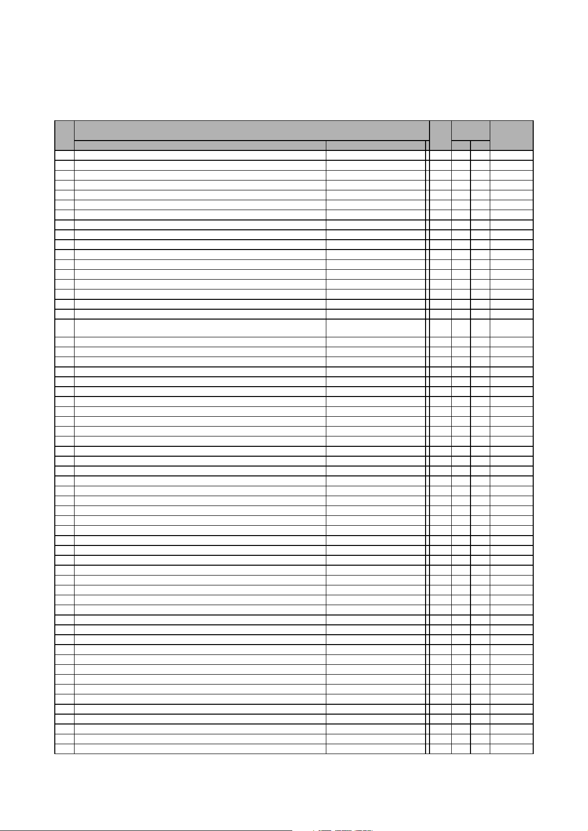
180 Sub Contrast 1 Except 15kHz system (15kHz→#262) 15 0 0 TA1391FG
181 Sub Contrast 1 DTT 15 0 0 TA1391FG
182 Sub Contrast 2 15 0 0 TA1391FG
183 Sub Contrast 2 DTT 15 0 0 TA1391FG
184 Sub Color 1 15 0 12 TA1391FG
185 Sub Color 1 DTT 15 0 0 TA1391FG
186 Sub Color 2 15 0 8 TA1391FG
187 Sub Color 2 DTT 15 0 0 TA1391FG
188 HV THRU 1 NTSC/PAL/480i/576i/480p/576p 1 0 0 TA1391FG
189 HV THRU 1 1080i-50/60/720p 1 0 0 TA1391FG
190 HV THRU 2 NTSC/PAL/480i/576i/480p/576p 1 0 0 TA1391FG
191 HV THRU 2 1080i-50/60/720p 1 0 0 TA1391FG
192 H_SEP 1 RF/VIDEO 1 0 0 TA1391FG
193 H_SEP 1 480i/576i 1 0 0 TA1391FG
194 H_SEP 1 480p/576p 1 0 0 TA1391FG
195 H_SEP 1 1080i_50 1 0 0 TA1391FG
196 H_SEP 1 1080i_60/720p 1 0 0 TA1391FG
197 H_SEP 2 RF/VIDEO 1 0 0 TA1391FG
198 H_SEP 2 480i/576i 1 0 0 TA1391FG
199 H_SEP 2 480p/576p 1 0 0 TA1391FG
200 H_SEP 2 1080i_50 1 0 0 TA1391FG
201 H_SEP 2 1080i_60/720p 1 0 0 TA1391FG
202 V_SEP 1 RF/VIDEO 1 0 0 TA1391FG
203 V_SEP 1 480i/576i 1 0 0 TA1391FG
204 V_SEP 1 480p/576p 1 0 0 TA1391FG
205 V_SEP 1 1080i_50 1 0 0 TA1391FG
206 V_SEP 1 1080i_60/720p 1 0 0 TA1391FG
207 V_SEP 2 RF/VIDEO 1 0 0 TA1391FG
208 V_SEP 2 480i/576i 1 0 0 TA1391FG
209 V_SEP 2 480p/576p 1 0 0 TA1391FG
210 V_SEP 2 1080i_50 1 0 0 TA1391FG
211V_SEP 2 1080i_60/720p 1 0 0 TA1391FG
212 AFC MODE 1 RF 3 0 0 TA1391FG
213 AFC MODE 1 VIDEO 3 0 0 TA1391FG
214 AFC MODE 2 RF 3 0 0 TA1391FG
215 AFC MODE 2 VIDEO 3 0 0 TA1391FG
216 N_LVL 1 RF 1 0 0 TA1391FG
217 N_LVL 1 VIDEO 1 0 0 TA1391FG
218 N_LVL 2 RF 1 0 0 TA1391FG
219 N_LVL 2 VIDEO 1 0 0 TA1391FG
220 HD POSITION 1 480i/576i 15 0 0 TA1391FG
221 HD POSITION 1 480p/576p 15 0 0 TA1391FG
222 HD POSITION 1 1080i_50 15 0 0 TA1391FG
223 HD POSITION 1 1080i_60/720p 15 0 0 TA1391FG
224 HD POSITION 2 480i/576i 15 0 0 TA1391FG
225 HD POSITION 2 480p/576p 15 0 0 TA1391FG
226 HD POSITION 2 1080i_50 15 0 0 TA1391FG
227 HD POSITION 2 1080i_60/720p 15 0 0 TA1391FG
228 Y LPF 1 RF 1 1 1 TA1391FG
229 Y LPF 1 VIDEO 1 1 1 TA1391FG
230 Y LPF 2 RF 1 1 1 TA1391FG
231 Y LPF 2 VIDEO 1 1 1 TA1391FG
232 Gain 1 1 1 1 TA1391FG
233 Gain 2 1 1 1 TA1391FG
234 HD/VD OUTPUT LEVEL 1 1 1 TA1391FG
235 Video2-RGB MODE ON For ASIA 1 0 0 -
236 Heat APC function (HAPC) available 1 1 1 PDP
237 γ-select(0:1.0, 1:2.2, 2:2.8) RF/VIDEO 2 1 1 PDP
238 γ-select(0:1.0, 1:2.2, 2:2.8) DSUB-RGB 2 1 1 PDP
239 Select for APC function 1 0 0 PDP
ADJ. Items Mode PDP LCD
Function
Max.
value
Init. Value
Device
15

42PD8800/32LD8800
Adj.
No
240 CCFMD function RF/VIDEO 1 0 0 PDP
241 CCFMD function DSUB-RGB 1 0 0 PDP
242 NTSC/EBU(CCFORM) SD(YCbCr)/Scart-RGB 1 0 0 PDP
243 NTSC/EBU(CCFORM) HD(YPbPr) 1 0 0 PDP
244 NTSC/EBU(CCFORM) DSUB-RGB 1 0 0 PDP
245 Correction for Tracking (DCBON) RF/VIDEO-Color Temp. Cool 1 1 1 PDP
246 Correction for Tracking (DCBON) RF/VIDEO-Color Temp. Nor/War 1 1 1 PDP
247 Correction for Tracking (DCBON) DSUB-RGB 1 1 1 PDP
248 Color Temp. Correction 3 2 2 PDP
249 Brightness Limitted Function of PANEL [APSON] 1 1 1 PDP
250 Dispersion Time of Sustain current 0:2 Times, 1:4 times For Dynamic mode 1 0 0 PDP
251 Dispersion Time of Sustain current 0:2 Times, 1:4 times For Natural mode 1 1 1 PDP
252 Dispersion Time of Sustain current 0:2 Times, 1:4 times For Cinema mode 1 1 1 PDP
253 Dispersion Time of Sustain current 0:2 Times, 1:4 times For PC mode 1 1 1 PDP
254 Dispersion Time of Sustain current 0:2 Times, 1:4 times For PC-Movie mode 1 1 1 PDP
255 Q mode 0:Freeze, 1:Move 1, 2:Move 2, 3:Movie3 For 50Hz[Dynamic] mode 3 2 1 PDP
256 Q mode 0:Freeze, 1:Move 1, 2:Move 2, 3:Movie3 For 50Hz[Natural] mode 3 3 1 PDP
257 Q mode 0:Freeze, 1:Move 1, 2:Move 2, 3:Movie3 For 50Hz[Cinema] mode 3 3 1 PDP
258 Q mode 0:Freeze, 1:Move 1, 2:Move 2, 3:Movie3 For 60Hz[Dynamic] mode 3 2 1 PDP
259 Q mode 0:Freeze, 1:Move 1, 2:Move 2, 3:Movie3 For 60Hz[Natural] mode 3 3 1 PDP
260 Q mode 0:Freeze, 1:Move 1, 2:Move 2, 3:Movie3 For 60Hz[Cinema] mode 3 3 1 PDP
261 Q mode 0:Freeze, 1:Move 1, 2:Move 2, 3:Movie3 For 70Hz(PC) 3 0 0 PDP
262 Sub Contrast 1 15kHz System 15 4 4 TA1391FG
263 Vak OFfSet (Vak_OFS) 255 0 0 PDP
264 Vak to Vra Parameter(VaktoVra) 255 1 1 PDP
265 Vsk to Vrs Parameter(VsktoVrs) 255 1 1 PDP
266 VFB WAIT CounTer(CT_VWAIT) 255 60 60 PDP
267 VFB CORRection Counter(CT_VCORR) 255 15 15 PDP
268 Vsk OFFSet(Vsk_OFS) 255 0 0 PDP
269 Uvrs/Uvra RECALL(RCLVr) 1 0 0 PDP
270 C3OTON 1:ON, 0:OFF 1 1 1 PDP
271 C3OTLV 1:ON, 0:OFF 1 1 1 PDP
272 SRV16 1:ON, 0:OFF 1 0 0 PDP
273 WTI-VW 1:ON, 0:OFF 1 0 0 PDP
274 WTI-WAVE 0:AUTO1, 1:AUTO2, 2:Fix 2 0 0 PDP
275 SRV17 0:ON, 1:OFF 1 0 0 PDP
276 Vsk DETect First 2Bits(Vsk_DET) - - - PDP
277 Vsk DETect Last 8Bits(Vsk_DET) - - - PDP
278 Vsk detect INIT. First 2Bits(Vsk_INIT) - - - PDP
279 Vsk detect INIT. Last 8Bits(Vsk_INIT) - - - PDP
280 Vak DETect First 2Bits(Vak_DET) - - - PDP
281 Vak DETect Last 8Bits(Vak_DET) - - - PDP
282 DeLTa Vrs value(DLT_Vrs) - - - PDP
283 DeLTa Vra value(DLT_Vra) - - - PDP
284 Vak detect INIT. First 2Bits(Vak_INIT) - - - PDP
285 Vak detect INIT. Last 8Bits(Vak_INIT) - - - PDP
286 USER Vrs(Uvrs) - - - PDP
287 USER Vra(Uvra) - - - PDP
288 ISM Limit Limit Value 0:1023 1:580 1 0 0 WVGA
289 ISM Control for WVGA For WVGA 1 1 1 WVGA
290 SWIVEL DEMO MODE ON 50 0 0 291 WVGA BRIGHTNESS For WVGA 1 0 0 WVGA
292 Black insert function 0:Not available, 1:Available
293 Dynamic Backlight function 0:No, 1:Yes For LCD 1 1 1 M30627
294 →HDMI Setup 0:None VGA/Others Yes, 1:All none 2:All have →HDMI 2 0 0 M30627
295 DTT LOG ENABLE For DTT 1 0 0 296 AUTO_FM/AM (D11-D8) - 15 2 2 MSP3455G
297 AUTO_FM/AM (D 7-D0) - 254 189 189 MSP3455G
298 A2_THRESHOLD (D11-D8) - 15 0 0 MSP3455G
299 A2_THRESHOLD (D 7-D0) - 254 112 112 MSP3455G
ADJ. Items Mode PDP LCD
Function
For LCD Dynamic mode or Day
mode
Init. Value
Max.
value
1 0 0 M30627
Device
16
42PD8800/32LD8800
Adj.
No
300 PRE_AM
301 VOL_SCART1 (D15-D8) - 254 115 115 MSP3455G
302 VOL_SCART1 (D 7-D5) - 7 0 0 MSP3455G
303 PRE_SCART - 254 31 31 MSP3455G
304 PRE_FM 4.5MHz(JAPAN) 254 34 34 MSP3455G
305 PRE_FM
306 PRE_FM 4.5MHz(BTSC-SAP) 254 60 60 MSP3455G
307 PRE_FM
308 PRE_FM 4.5MHz(KOREA-Dual/Stereo) 254 34 34 MSP3455G
309 PRE_FM
310 PRE_FM
311PRE_NICAM - 254 57 57 MSP3455G
312 CM_THRESHOLD (D15-D8) - 254 0 0 MSP3455G
313 CM_THRESHOLD (D7 -D0) - 254 36 36 MSP3455G
314 Sound Multiplex special operation (0:Normal 1:Korea) 1 0 0 M30627
315 Set Stereo jugdment level at turn on mode of Sound Multiplex For Korea special version 127 18 18 M30627
316 Set Dual judgment level at turn on mode of Sound Multiplex For Korea special version 128 18 18 M30627
317 Set Stereo jugdment level at normal mode of Sound Multiplex For Korea special version 127 18 18 M30627
318 Set Dual judgment level at normal mode of Sound Multiplex For Korea special version 128 18 18 M30627
319 Set jugdment time for jugd to Multiplex at turn on mode For Korea special version 255 117 117 M30627
320 Set Counting time for jugdmenet of normal mode For Korea special version 255 10 10 M30627
321 Set jugdment time for jugd to Multiplex at normal mode For Korea special version 255 64 64 M30627
322 Select over modulated mode For Korea special version 2 0 0 M30627
323 Set over modulated mode 1 For Korea special version 255 18 18 MSP3455G
324 Set over modulated mode 2 For Korea special version 255 32 32 MSP3455G
325 TEXT H sync delay - 127 0 0 SAA5361
326 TEXT V sync delay - 127 50 50 SAA5361
327 TEXT_H_POSITION - 254 48 48 SAA5361
328 TEXT_V_POSITION - 254 39 39 SAA5361
329 Select for APC output [Except Europe model] Main RF 2 1 1 SAA5361
330 L_PLL.GAIN 1 0 0 TDA9885
331 HDMI EDID WRITE ENABLE s 1 0 0 M30627
HDMI Ccolorimetry Judgement 0:Signal Format Priority/1:AVI
332
InfoFrame Priority
333 BPMA : Back Porch Mode,Field2 Position Adjustment 1 1 1 HDMI
334 TMDS Equalization Control (0:0xC3, 1:0x0F, 2:0x1E, •••, 16:0xF0) 16 13 13 HDMI
Select HDMI 1/2 at no using 0: Both no select,1:Select HDMI 1, 2:
335
Select HDMI 2
336 PRMB : preamble criteria 31 6 6 HDMI
337 HDCP : HDCP enable criteria 31 12 12 HDMI
338 Picture Output Mode Select OUTTYP[1:0] 2 0 0 uPD64015
339 Digital LPF Through Control LPFTHR[1:0] 3 0 0 uPD64015
340 1 0 0 uPD64015
341 ADC Sampling Delay Setting ADCKS[1:0] 3 3 3 uPD64015
342 Clock Setting in Component Mode CPNFSC 1 1 1 uPD64015
343 Color System Change Detection Time Setting DETOUT[3:0] 15 4 4 uPD64015
344 Color System Judgement Time Setting DETTIM[3:0] 15 4 4 uPD64015
345 Burst Lock Detection Variable Setting CLKVA 1 1 1 uPD64015
346 Burst Lock Detection Condition Setting CLKLL[6:0] 127 37 37 uPD64015
347 ARI Gain Fine Adjustment R_GAIN[4:0] 31 16 16 uPD64015
348 FHD Output Delay Adjustment FHDDL[5:0] TEXT 63 20 20 uPD64015
349 FHD Output Range Setting FHDWD[1:0] TEXT 3 1 1 uPD64015
350 FVD Output Delay Adjustment1 FVDDL[2:0] TEXT 7 7 7 uPD64015
351 FVD Output Delay Adjustment2 FVDHDL[2:0] TEXT 7 1 1 uPD64015
352 For Europe : Transmission of Station Name Check Command 2 0 0 SAA5361
353 For Europe : Result of Station Name Check - - - SAA5361
354 Pedestal Level Correction Sensitivity Adjustment PEDIIRS2 1 0 0 uPD64015
355 AGI Gain Fine Adjusstment G_GAIN[4:0] 31 16 16 uPD64015
356 Jitter Filter Select FLTSEL[1:0] 3 0 0 uPD64015
357 ABI Gain Fine Adjustment B_GAIN[4:0] 31 16 16 uPD64015
FB Signal Input Delay Adjustment 4BH:FBCNT[2:1] & 4CH:
358
FBCNT[0]
Analog RGB Signal Input Delay Adjustment 4Ch:RGBCNT[2] &
359
4Dh:4Ch:RGBCNT[1:0]
ADJ. Items Mode PDP LCD
Function
Except 4.5MHz (Except Dual/
Stereo mode)
4.5MHz(Except BTSC-SAP
mode)
4.5MHz(Except KOREA-Dual/
Stereo mode)
Except 4.5MHz(Except Dual/
Stereo mode)
Except 4.5MHz(Dual/Stereo
mode)
HDMI 1 0 0 HDMI
Init. Value
Max.
value
254 17 17 MSP3455G
254 32 32 MSP3455G
254 36 36 MSP3455G
254 17 17 MSP3455G
254 27 27 MSP3455G
2 0 0 HDMI
7 0 0 uPD64015
7 0 0 uPD64015
Device
17
42PD8800/32LD8800
Adj.
No
360
Sub Contrast Gain Adjustment SBCNT[5:0] 63 32 32 uPD64015
361
Sub Color Cb Gain Adjustment CBGAIN[5:0] 63 32 32 uPD64015
362
Sub Color Cr Gain Adjustment CRGAIN[5:0] 63 32 32 uPD64015
363
YGC Auto Mode Select YGCAUTO 1 0 0 uPD64015
364
YGC Manual Gain Value Setting YGCVAL[6:0] 127 58 58 uPD64015
365
YGC Select YGCOFF 1 0 0 uPD64015
366
YGC Control Mode Select1 YGCMVS 1 0 0 uPD64015
367
Progressive Y Signal Gain Select YPGAINS[1:0] 3 1 1 uPD64015
368
YGC Control Mode Select YGCAVAL[6:0] 31 9 9 uPD64015
369
YGC Control Mode Select2 MAXIIRS 1 0 0 uPD64015
370
DC Level Control Mode Select PEDIIRS[1:0] 3 1 1 uPD64015
371
YGC Control Mode Select4 YGCIIRS[1:0] 3 1 1 uPD64015
372
Vertical Sync Signal Slice Level Setting VSYLSE[3:0] RF 15 10 10 uPD64015
373
374
375
Horizontal Sync Signal Slice Level Setting SYLSE[3:0] RF 15 9 9 uPD64015
376
377
378
Sync Slice Slice Level Setting for Progressive PSYLSE[3:0] 15 9 9 uPD64015
379
Vertical Sync Signal Detection Range Setting VDETTIM 1 0 0 uPD64015
380
Vertical Sync Signal Detection Correction Setting VDETG 1 1 1 uPD64015
381
Horizontal Sync Signal False Detection Prevention Setting MASKHD 1 1 1 uPD64015
382
Vertical Sync Output Switching for Digital RGB VDFB 1 0 0 uPD64015
383
Noise Level Detection Characteristic Setting1 NDUMODE 1 0 0 uPD64015
384
Noise Level Detection Characteristic Setting2 NDUD2H 1 0 0 uPD64015
385
Noise Level Detection Sensitivity Setting1 NDUWSC[1:0] 3 1 1 uPD64015
386
Noise Level Detection Sensitivity Setting2 NDUXSC[1:0] 3 1 1 uPD64015
387
3 Dimentional Y/C Separate Operation Mode Select NSDS[1:0] 3 0 0 uPD64015
388
Line Comb Filter Operation Mode YCSV[1:0] 3 0 0 uPD64015
389
3 Line Comb Select Sensitivity Setting1 VCOMA[1:0] 3 2 2 uPD64015
390
3 Line Comb Select Sensitivity Setting2 VCOMB[1:0] 3 2 2 uPD64015
391
Y Trap Filter Characteristic Select (NTSC, PAL) YCSHY[1:0] 3 0 0 uPD64015
392
C Separate Filter Characteristic Select (NTSC, PAL) YCSHC[1:0] 3 0 0 uPD64015
393
Chroma Output Filter Processing Select COBPFOFF 1 0 0 uPD64015
Chroma Output Frequency Characteristic Correction Select
394
YCSCOF[2:0]
395
Y Trap Filter Select (SECAM) YCSSY[2:0] 6 0 0 uPD64015
396
Vertical Logical Comb Select Sensitivity Setting VLTYPE 1 1 1 uPD64015
397
C Separate Filter Select (SECAM) YCSSC[2:0] 6 0 0 uPD64015
398
Aperture Select VAPONV 1 1 1 uPD64015
399
V Aperture Gain Select VAPG[2;0] RF 7 2 5 uPD64015
400
401
402
V Aperture Convergent Point Setting VAPI[4:0] 31 20 20 uPD64015
403
PAL Color Phase Distortion Correction Select PALCFIL[1:0] 3 0 0 uPD64015
404
Y Signal 2fc Denoising Effect Select YCSY2F[1:0] 3 3 3 uPD64015
405
Y/C timing for L(6.5) system RF Main 15 8 8 uPD64015
406
Trap Filter Select TRF[1:0] 3 0 0 uPD64015
407
Trap Filter Gain Setting TRGAIN[2:0] 7 0 0 uPD64015
408
Trap Filter Setting TRPAL 1 0 0 uPD64015
409
Y/C timing for L'(6.5) system RF Main 15 8 8 uPD64015
410
Motion Detection Mode Setting MSS[1:0] 3 0 0 uPD64015
411
Y Motion Detection Coring Setting DYCOR[3:0] NTSC 15 2 2 uPD64015
412
Y Motion Detection Coring Setting DYCOR[3:0] Except NTSC mode 15 3 3 uPD64015
413
Y Motion Detection Gain Setting DYGAIN[3:0] NTSC 15 9 9 uPD64015
414
Y Motion Detection Gain Setting DYGAIN[3:0] Except NTSC mode 15 9 9 uPD64015
415
C Motion Detection Coring Setting DCCOR[3:0] NTSC 15 3 3 uPD64015
416
C Motion Detection Coring Setting DCCOR[3:0] Except NTSC mode 15 2 2 uPD64015
417
C Motion Detection Gain Setting DCGAIN[3:0] NTSC 15 6 6 uPD64015
418
C Motion Detection Gain Setting DCGAIN[3:0] Except NTSC mode 15 11 11 uPD64015
419
Motion Detection Characteristic Test1 SELYCLM[1:0] 3 1 1 uPD64015
ADJ. Items Mode PDP LCD
Function
AV 15 10 10 uPD64015
480i/576i 15 10 10 uPD64015
AV 15 9 9 uPD64015
480i/576i 15 9 9 uPD64015
AV 7 5 4 uPD64015
480i/576i 7 6 4 uPD64015
Init. Value
Max.
value
4 0 0 uPD64015
Device
18
42PD8800/32LD8800
Adj.
No
420 Motion Detection Characteristic Test2 SELDYH2F 1 0 0 uPD64015
421 Motion Detection Characteristic Test3 SELDCH2F 1 1 1 uPD64015
422 Motion Detection Characteristic Test6 SELD1FL 1 0 0 uPD64015
423 Color Demodulation Burst Gate Pulse Range Setting BGP2WD[3:0] 15 10 10 uPD64015
424 Color Demodulation Burst Gate Pulse Starting Point Setting BGP2ST[3:0] 15 8 8 uPD64015
425 Demodulation Part Force Killer Setting KILON 1 0 0 uPD64015
426 Time Constant Setting for Color Demodulation APC APCGAIN[1:0] 3 1 1 uPD64015
427 Time Constant Setting for Color Demodulation ACC ACCGAIN[1:0] 3 1 1 uPD64015
428 Control Characteristic Setting for Color Demodulation ACC ACCLIM[3:0] 15 8 8 uPD64015
429 SECAM Burst Pulse Position Correction SBGTDL[2:0] 7 7 7 uPD64015
430 PAL Line Detection Strength Setting PIDSTR[4:0] 31 4 4 uPD64015
431 SECAM Line Detection Strength Setting SIDSTR[4:0] 31 8 8 uPD64015
432 SECAM System Judgement Strength Setting SDETSTR[7:0] 255 168 168 uPD64015
433 3DNR Mode Setting NRMODE[1:0] 3 2 2 uPD64015
434 YNR Process Stop YNRSTOP 1 1 1 uPD64015
435 YNRLPF Process Yes/No YNRLPFON 1 0 0 uPD64015
436 YNR Nonlinear Filter Gain Setting YNRGAIN[1:0] 3 2 2 uPD64015
437 YNR Nonlinear Filter Convergence Level Setting YNRCORE[2:0] 7 3 3 uPD64015
438 YNR Nonlinear Filter Limit Level Setting YNRLIM[2:0] 7 3 3 uPD64015
439 YNR Motion Detection between Frames Coring Setting YMVDCORE[3:0] 15 6 6 uPD64015
440 YNR Motion Detection between Frames Gain Setting YNRMVDG[3:0] 15 6 6 uPD64015
441 YNR Motion Detection between Frames Setting YNRMDOFF 1 1 1 uPD64015
442 CNR Process Stop CNRSTOP 1 1 1 uPD64015
443 CNRLPF Process Yes/No CNRLPFON 1 0 0 uPD64015
444 CNR Nonlinear Filter Gain Setting CNRGAIN[1:0] 3 3 3 uPD64015
445 CNR Nonlinear Filter Convergence Level Setting CNRCORE[2:0] 7 3 3 uPD64015
446 CNR Nonlinear Filter Limit Level Setting CNRLIM[2:0] 7 3 3 uPD64015
447 CNR Motion Detection between Frames Coring Setting CMVDCORE[3:0] 15 4 4 uPD64015
448 CNR Motion Detection between Frames Gain Setting CNRMVDG[3:0] 15 4 4 uPD64015
449 CNR Motion Detection between Frames Setting CNRMDOFF 1 1 1 uPD64015
450 Setup Level Correction Setting1 STNTSCM RF 1 0 0 uPD64015
451 AV(Except 480i/576i) 1 0 0 uPD64015
452 AV(480i/576i) 1 0 0 uPD64015
453 Setup Level Correction Setting2 STPALD[2:0] RF 7 0 0 uPD64015
454 AV(Except 480i/576i) 7 0 0 uPD64015
455 AV(480i/576i) 7 0 0 uPD64015
456 Sub Contrast Adjustment SBCNT[7:0] RF(M) 255 128 108 uPD64015
457 RF(BG) 255 128 108 uPD64015
458 RF(DK) 255 128 108 uPD64015
459 RF(I) 255 128 108 uPD64015
460 RF(LL') 255 128 108 uPD64015
461 AV(Except 480i/576i) 255 128 108 uPD64015
462 AV(480i/576i) 255 128 128 uPD64015
463 Sub Color Adjustment for Cb SBCLRU[7:0] RF 255 128 128 uPD64015
464 AV(Except 480i/576i) 255 128 128 uPD64015
465 AV(480i/576i) 255 128 128 uPD64015
466 Sub Color Adjustment for Cr SBCLRV[7:0] RF 255 128 128 uPD64015
467 AV(Except 480i/576i) 255 128 128 uPD64015
468 AV(480i/576i) 255 128 128 uPD64015
469 Y Noise Coring1 YCONR[3:0] NTSC 10 0 0 uPD64015
470 Except NTSC 10 0 0 uPD64015
471 480i/576i 10 0 0 uPD64015
472 C Noise Coring1 CCONR[3:0] NTSC 8 0 0 uPD64015
473 Except NTSC 8 4 4 uPD64015
474 480i/576i 8 0 0 uPD64015
475 Brightness Signal Noise Coring2 YCORB[3:0] NTSC 10 0 0 uPD64015
476 Except NTSC 10 0 0 uPD64015
477 480i/576i 10 0 0 uPD64015
478 Brightness Signal Noise Coring2 Control YCOREN NTSC 1 1 1 uPD64015
479 Except NTSC 1 1 1 uPD64015
ADJ. Items Mode PDP LCD
Function
Max.
value
Init. Value
Device
19

42PD8800/32LD8800
Adj.
No
480 480i/576i 1 1 1 uPD64015
481 Brightness Signal Noise Coring (highpass) YCORH[2:0] NTSC 7 0 0 uPD64015
482 Except NTSC 7 0 0 uPD64015
483 480i/576i 7 0 0 uPD64015
484 Color-Difference Signal Noise Coring2 CCORB[3:0] NTSC 10 0 0 uPD64015
485 Except NTSC 10 0 0 uPD64015
486 480i/576i 10 0 0 uPD64015
487 Color-Difference Signal Noise Coring2 Control CCOREN NTSC 1 0 0 uPD64015
488 Except NTSC 1 0 0 uPD64015
489 480i/576i 1 0 0 uPD64015
490 LTI Correction Amount Adjustment LTIGAIN[3:0] RF(M) 15 0 0 uPD64015
491 RF(Except M) 15 0 0 uPD64015
492 NTSC 15 0 0 uPD64015
493 Except NTSC 15 1 1 uPD64015
494 480i/576i 15 0 0 uPD64015
495 CTI Correction Amount Adjustment CTIGAIN[3:0]
496 RF(Except M) 15 0 0 uPD64015
497 NTSC 15 0 0 uPD64015
498 Except NTSC 15 7 7 uPD64015
499 480i/576i 15 0 0 uPD64015
500 Filter Setting for LTI LTITAP[2:0] RF(M) 7 2 2 uPD64015
501 RF(Except M) 7 2 2 uPD64015
502 NTSC 7 2 2 uPD64015
503 Except NTSC 7 1 1 uPD64015
504 480i/576i 7 7 7 uPD64015
505 Coring Setting for LTI LTICORE[3:0] NTSC 11 3 3 uPD64015
506 Except NTSC 11 3 3 uPD64015
507 480i/576i 11 3 3 uPD64015
508 Filter Setting for CTI CTITAP[2:0] RF(M) 7 2 2 uPD64015
509 RF(Except M) 7 2 2 uPD64015
510 NTSC 7 2 2 uPD64015
511 Except NTSC 7 5 5 uPD64015
512 480i/576i 7 2 2 uPD64015
513 Coring Setting for CTI CTICORE[3:0] RF(M) 9 3 3 uPD64015
514 RF(Except M) 9 3 3 uPD64015
515 NTSC 9 3 3 uPD64015
516 Except NTSC 9 3 3 uPD64015
517 480i/576i 9 3 3 uPD64015
518 Sharpness Adjustment SHPGAIN[7:0] RF(M) 255 150 160 uPD64015
519 RF(BG) 255 150 150 uPD64015
520 RF(DK) 255 150 160 uPD64015
521 RF(I) 255 160 170 uPD64015
522 RF(LL') 255 150 160 uPD64015
523 TEXT 255 128 128 uPD64015
524 NTSC(Ex.S Input)→S:#692 255 150 140 uPD64015
525 Except NTSC(Ex.S Input)→S:#693 255 130 140 uPD64015
526 480i/576i →576i:#694 255 130 140 uPD64015
527 Filter Setting for Sharpness SHPCHAR[2:0] RF 6 3 3 uPD64015
528 NTSC 6 3 3 uPD64015
529 Except NTSC 6 3 3 uPD64015
530 TEXT 6 3 3 uPD64015
531 480i/576i 6 3 3 uPD64015
532 Coring Setting for Sharpness SHPCORE[3:0] RF 10 0 0 uPD64015
533 NTSC 10 0 0 uPD64015
534 Except NTSC 10 0 0 uPD64015
535 TEXT 10 0 0 uPD64015
536 480i/576i 10 0 0 uPD64015
537 Luminance Adjustment (First 8Bits) BRIGHT[9:2] NTSC mode 255 128 128 uPD64015
538 Luminance Adjustment (First 8Bits) BRIGHT[9:2] Except NTSC mode 255 128 128 uPD64015
539 Luminance Adjustment (First 8Bits) BRIGHT[9:2] 480i/576i 255 128 128 uPD64015
ADJ. Items Mode PDP LCD
Function
RF(M) *In substitution for M Group
Delay of Correction
Init. Value
Max.
value
15 0 0 uPD64015
Device
20
42PD8800/32LD8800
Adj.
No
540 Luminance Adjustment (Last 2Bits) BRIGHT[1:0] NTSC mode 3 0 0 uPD64015
541 Luminance Adjustment (Last 2Bits) BRIGHT[1:0] Except NTSC mode 3 0 0 uPD64015
542 Luminance Adjustment (Last 2Bits) BRIGHT[1:0] 480i/576i 3 0 0 uPD64015
543 R-Y Axis Adjustment OFRY[5:0] NTSC 63 32 32 uPD64015
544 Except NTSC 63 32 32 uPD64015
545 Color Adjustment COLORG[7:0] RF(M) 255 115 110 uPD64015
546 RF(BG) 255 120 110 uPD64015
547 RF(DK) 255 120 110 uPD64015
548 RF(I) 255 120 110 uPD64015
549 RF(LL') 255 120 110 uPD64015
550 TEXT 255 128 128 uPD64015
551 NTSC 255 120 138 uPD64015
552 Except NTSC 255 123 134 uPD64015
553 480i/576i 255 128 128 uPD64015
554 Tint Adjustment HUE[7:0] RF(M) 255 150 135 uPD64015
555 RF(Except M) 255 128 128 uPD64015
556 NTSC(Ex.S Input)→S:#695 255 126 128 uPD64015
557
558 480i 255 125 128 uPD64015
559 576i 255 130 130 uPD64015
560 Contrast Adjustment CONT[7:0] NTSC 255 108 118 uPD64015
561 Except NTSC 255 108 118 uPD64015
562 480i/576i 255 114 108 uPD64015
563 APL Detection Line Setting APLWID[5:0] 50Hz 63 0 0 uPD64015
564 60Hz 63 0 0 uPD64015
565 APL Detection Time Constant Setting APLCOE[3:0] 50Hz 15 5 5 uPD64015
566 60Hz 15 5 5 uPD64015
567 Direct Transmission Rate Correction Amount Setting DCREGAIN[3:0] 15 8 8 uPD64015
568 Black Stretch Correction Amount Setting BLEXGAIN[5:0] 63 16 16 uPD64015
569 Black Stretch Correction APL Adaptive Amount ABLEXST[3:0] 15 0 0 uPD64015
570 Black Stretch Correction Operation Point Setting BLEXST[7:0] 255 0 0 uPD64015
571 White Peak Correction Amount Setting GAMGAIN[3:0] 15 0 0 uPD64015
572 White Peak Correction APL Adaptive Amount Setting AGAMGAIN[3:0] 15 0 0 uPD64015
573 White Peak Correction Operation Point Setting GAMST[7:0] 255 255 255 uPD64015
574 Black Stretch Correction Setting BLEXCTL 1 0 0 uPD64015
575 White Peak Correction Setting YGAMCTL 1 0 0 uPD64015
576 ACL Correction Amount Setting ACLSEN[3:0] 15 0 0 uPD64015
577 ACL Correction Operation Point Setting ACLST[7:0] 255 255 255 uPD64015
578 Image Blanking Setting YVBCTL 1 1 1 uPD64015
579 LPF Characteristic Setting for Color-Difference CR Signal CRLPF[1:0] 3 1 1 uPD64015
580 LPF Characteristic Setting for Color-Difference Cb Signal CBLPF[1:0] 3 1 1 uPD64015
581 Burst Gate Pulse Range Setting BGPWD[3:0] NTSC 15 8 8 uPD64015
582 Except NTSC 15 8 8 uPD64015
583 Burst Gate Pulse Starting Point Setting BGPST[3:0] NTSC 15 8 8 uPD64015
584 Except NTSC 15 8 8 uPD64015
585 Killer Level Setting KILLV[3:0] RF NTSC 15 8 8 uPD64015
586 RE PAL 15 8 8 uPD64015
587 RF SECAM 15 8 8 uPD64015
588 AV NTSC 15 3 3 uPD64015
589 AV PAL 15 3 3 uPD64015
590 AV SECAM 15 3 3 uPD64015
591 Killer Level Setting for Color System Judgement KILLVCTL[3:0] RF NTSC 15 9 9 uPD64015
592 RF PAL 15 9 9 uPD64015
593 RF SECAM 15 9 9 uPD64015
594 AV NTSC 15 9 9 uPD64015
595 AV PAL 15 9 9 uPD64015
596 AV SECAM 15 9 9 uPD64015
597 Burst Lock PLL Gain Setting FSCFGAN 1 1 1 uPD64015
598 Phase Error Detection Setting for Burst Lock FSCSYC 1 0 0 uPD64015
599 Burst Lock PLL Phase Error Detection Level Setting GAINSEL 1 0 0 uPD64015
ADJ. Items Mode PDP LCD
Function
Except NTSC(Ex.S Input)→
S:#696
Init. Value
Max.
value
255 124 133 uPD64015
Device
21

42PD8800/32LD8800
Adj.
No
600 Vertical Sync Signal Pull-in Range Select VLIM 1 0 0 uPD64015
601 V Counter Free Run Setting at No Signal Mode NSGVFRUN 1 1 1 uPD64015
602 Line Lock Clock Free Run Settng at No Signal Mode NSGFRUN 1 0 0 uPD64015
603 Vertical Sync Signal Correction VDCOR 1 0 0 uPD64015
604 Line Lock PLL Gain Setting HPLLG[4:0] RF 31 3 3 uPD64015
605 Line Lock PLL Phase Detection Condition Setting HPLLSIG 1 0 0 uPD64015
606 Line Lock PLL Response Correction Setting HPLLH2 1 1 1 uPD64015
607 Line Lock PLL Response Correction Coeffi cient1 HPLLH21[7:0] 255 32 32 uPD64015
608 Line Lock PLL Response Correction Coeffi cient2 HPLLH22[7:0] 255 8 8 uPD64015
609 PWM Select for Clamp PWMSEL[1:0] 3 3 3 uPD64015
610 Motion Detection Gain Setting D2FGAIN[2:0] NTSC 7 5 5 uPD64015
Motion Detection Coring Setting D2FCOR[6:0] (3D Comb.= for High/Low&OFF
611
→0)
612 Except NTSC mode 127 7 7 uPD64015
613 Motion Detection Characteristic Test8 C2O NTSC mode 1 0 0 uPD64015
614 Offset Substraction Value(NR=ON) for Sharpness Adjustment(#518~522) RF (NR=ON) 63 50 50 uPD64015
615 Motion Detection Characteristic Test9 MDMVD NTSC mode 1 0 0 uPD64015
616 Motion Detection LPF Setting MVDLPFON 1 0 0 uPD64015
617 Motion Detection H Black Stretch Setting TESDOT[2:0] NTSC 7 0 0 uPD64015
618 Except NTSC 7 0 0 uPD64015
619 Y Motion Detection Gain Setting CLIPSELY[1:0] NTSC 3 1 1 uPD64015
620 Except NTSC mode 3 2 2 uPD64015
621 C Motion Detection Gain Setting CLIPSELC[1:0] NTSC 3 3 3 uPD64015
622 Except NTSC mode 3 3 3 uPD64015
623 Nonlinear Filter Setting1 NFP_3[3:0] NTSC 15 3 3 uPD64015
624 Except NTSC mode 15 5 5 uPD64015
625 Nonlinear Filter Setting2 NFP_7[3:0] NTSC 15 7 7 uPD64015
626 Except NTSC mode 15 9 9 uPD64015
627 Nonlinear Filter Setting3 NFP_B[3:0] NTSC 15 10 10 uPD64015
628 Except NTSC mode 15 10 10 uPD64015
629 Line Comb Filter Operation Mode YCSV_c[1:0] 3 0 0 uPD64015
630 3 Line Comb Select Sensitivity Setting1 VCOMA_c[1:0] 3 2 2 uPD64015
631 3 Line Comb Select Sensitivity Setting2 VCOMB_c[1:0] 3 2 2 uPD64015
632 BPF Select for Y/C Separate Chroma FIL15ON NTSC 1 0 0 uPD64015
633 Except NTSC mode 1 1 1 uPD64015
634 Logical Comb Bandwidth Setting for Brightness COMB_y NTSC 1 0 0 uPD64015
635 Except NTSC mode 1 0 0 uPD64015
636 Logical Comb Bandwidth Setting for Chroma COMB_c NTSC 1 0 0 uPD64015
637 Except NTSC mode 1 0 0 uPD64015
638 Vertical Logical Comb Select Sensitivity Setting VLTYPE_c NTSC 1 1 1 uPD64015
639 Except NTSC mode 1 1 1 uPD64015
640 Logical Comb Characteristic Select SELU 1 1 1 uPD64015
641 Setting for 1 Line Chroma Action ONE_CRMA NTSC 1 0 0 uPD64015
642 Except NTSC mode 1 1 1 uPD64015
643 Setting for 1 Line Chroma at Abnormal Condition OCRENNST NTSC 1 0 0 uPD64015
644 Except NTSC mode 1 0 0 uPD64015
645 Narrow Band BPF Setting for Chroma FIL15NAR 1 1 1 uPD64015
646 1 Line Chroma Detection Gain Setting V1PSEL[7:0] PAL 255 64 64 uPD64015
647 NTSC 255 64 64 uPD64015
648 SECAM 255 64 64 uPD64015
649 PAL-M 255 64 64 uPD64015
650 PAN-N 255 64 64 uPD64015
651 1 Line Chroma Coring Setting ONE_CROCOR[7:0] PAL 255 64 64 uPD64015
652 NTSC 255 64 64 uPD64015
653 SECAM 255 64 64 uPD64015
654 PAL-M 255 64 64 uPD64015
655 PAN-N 255 64 64 uPD64015
656 SECAM Filter Setting SDIEF_SEL[1:0] RF 3 0 0 uPD64015
657 AV 3 0 0 uPD64015
658 Trap Filter Setting at Abnormal Condition TRENNST RF 1 0 0 uPD64015
659 AV 1 0 0 uPD64015
ADJ. Items Mode PDP LCD
Function
NTSC mode 127 7 7 uPD64015
Max.
value
Init. Value
Device
22

42PD8800/32LD8800
Adj.
No
660 Y/C timing for M(4.5) system RF-Main 15 6 6 uPD64015
661 Y/C timing for (5.5MHz PAL/NTSC4.43) system RF Main 15 8 8 uPD64015
662 Y/C timing for (5.5MHz SECAM) system RF Main 15 8 8 uPD64015
663 Y/C timing for (6.0MHz PAL/NTSC4.43) system RF Main 15 8 8 uPD64015
664 Y/C timing for (6.0MHz SECAM) system RF Main 15 8 8 uPD64015
665 DAC Output Imapge Sync Comparison Setting DACLEVEL 1 0 0 uPD64015
666 Blanking Period Level Setting INBLK50IRE 1 0 0 uPD64015
667 Line Lock PLL Gain Setting HPLLG[4:0] AV 31 6 6 uPD64015
668 Motion Detection Gain Setting D2FGAIN[2:0] Except NTSC mode 7 5 5 uPD64015
669 Y/C timing for (6.5MHz PAL/NTSC4.43) system RF Main 15 8 8 uPD64015
670 HS Phase Setting for RGB Mix HSYNCDLY TEXT-1 Picture 1 1 1 uPD64015
671 Latter Part VS Phase Setting for RGB Mix VSDLY 1 0 0 uPD64015
672 SG Color Setting SGCOLOR[2:0] 7 0 0 uPD64015
673 SG Mode Setting (0:OFF/1:Ramp/2:Raster/3:STEP/4:BAR[75%]/5:[100%]) 5 0 0 uPD64015
674 Y/C timing for (6.5MHz SECAM) system RF Main 15 8 8 uPD64015
675 SG Level Setting SGPEDLEV 1 0 0 uPD64015
676 TEXT-2 Picture 1 1 1 uPD64015
677 Motion Detection Characteristic Test8 C2O Except NTSC mode 1 0 0 uPD64015
678 Motion Detection Characteristic Test9 MDMVD Except NTSC mode 1 0 0 uPD64015
679 Color Processing Status SETCOLOR[3:0] (READ Value) - - - uPD64015
680 Color System Detection Mode MODDET (READ Value) - - - uPD64015
681 Composite V Judgement-Input (0:no signal/1:50Hz/2:60Hz) - - - uPD64015
682 Composite V Judgement-Result (1:50Hz/2:60Hz) - - - uPD64015
683 No Signal Detection Characteristic Setting SIGDETLV 1 1 1 uPD64015
684 Image Input Signal Status Setting SIGON 1 0 0 uPD64015
685 Image Input Signal Status Setting SIGOFF 1 0 0 uPD64015
686 Field Frequency Setting TV50F 1 0 0 uPD64015
687 Field Frequency Setting TV60F 1 0 0 uPD64015
688 50 Hz Image Signal Sub Carrier 504M 1 0 0 uPD64015
689 50 Hz Image Signal Sub Carrier 503M 1 0 0 uPD64015
COLOR SYSTEM Judgement Method (0:Normal/1:System1&2 Correction has
690
no effect)
691 Sharpness Gain(TEXT-2 pictures) Sub 15 0 0 TB1274
692 Sharpness Adjustment SHPGAIN[7:0]
693
694 576i Separate from #526 255 130 130 uPD64015
695 Tint Adjustment HUE[7:0]
696
697 DCBLV (COOL) 1 1 1 PDP
698 DCBLV (NORMAL/WARM/B&W) 1 0 0 PDP
699 DCBLV (RGB) 1 0 0 PDP
700 Mode display 0:Normal, 1:RF mode only, 2:All 2 0 0 M30627
701 Horizontal Position of OSD 15 7 7 OSD
702 Vertical Position of OSD 15 7 7 OSD
703 Typical Value of Contrast OSD DYNAMIC 31 31 31 M30627
704 Temperature for Fun start (Temp_High) 254 58 58 TEMP
705 Temperature for Fun stop (Temp_Low) 254 55 55 TEMP
706 Display of internal temperature ºC (Temperature) 125 - - TEMP
707 Power Save/Screen Saver On/Off Setting at Initialize, Reset and Shipping
708 PC Power Save function (0:Impossible, 1:Possible) 1 1 1 M30627
Movement Amount of Image Retention Reduction Operation
709
0:±2pixel/1:±4pixel/2:±6pixel/3:±10pixel
710 480i,576i switch 0:uPD64015, 1:TA1391(Though) 1 0 0 TA1391FG
711Waite Time for POWER SAVE function (s) VIDEO/PC 254 15 15 M30627
712 BURN-IN enable/ disenable 0:Disenable, 1:Enable 1 1 1 M30627
713 BURN-IN mode 2 2 2 PDP
714 Recovery to an error of OSC frequency of Ceramic resonator for timer 62 34 34 M30627
715 EURO DK-SECAM MASK(V=60) 0:Normal 1:Mask(V=60) 1 0 0 716 Set Sound System at Auto mode of Sound Sys. (0:auto, 1:4.5MHz) Main 1 0 0 M30627
Power condition at power save mode of PC mode
717
after done RESET function
Select Wide mode for Europe model
718
(Normal= 5mode/ For Service= 10 mode)
719 Thermo sensor function available or not 0:None, 1:Yes 1 0 0 M30627
ADJ. Items Mode PDP LCD
Function
NTSC(S Input) Separate from
#524
Except NTSC(S Input)
Separate from #525
NTSC(S Input) Separate from
#556
Except NTSC(S Input)
Separate from #557
P.S/S.S
0:Off/20m
1:On/Off
2:Off/Off
Adjustment Value is available
only during HD single picture
mode.
0:Keep last condition,
1:Return to normal condition
0:Normal, 1:For service 1 0 0 M30627
Max.
Init. Value
value
1 0 0 uPD64015
255 150 125 uPD64015
255 155 125 uPD64015
255 130 133 uPD64015
255 124 137 uPD64015
2 0 0 M30627
300 FC
1 0 0 M30627
Device
23
42PD8800/32LD8800
Adj.
No
720 EURO SOUND SYSTEM DK Disable 0:Enable, 1Disable 1 0 0 M30627
721 Remote Function available 0:NO, 1:YES 1 1 1 M30627
722 Key Function available 0:NO, 1:YES 1 1 1 M30627
723 Terminal Mode Function available 0:Not Available, 1:Available RS232C 1 1 1 M30627
Set Taiwan/Korea/South America 0:Others 1: Taiwan/Korea/South
724
America
725 Language (Refer to below) 10 0 0 M30627
726 Hotel Mode(0:No, 1:Yes) 2 0 0 M30627
727 Initial Audio Level available (0:No 1: Yes) 1 0 0 M30627
728 Initial Audio Level 63 20 20 M30627
729 Size button available (0:No 1:Yes) 1 1 1 M30627
730 Multi Picture button available (0:No 1:Yes) 1 1 1 M30627
731 Photo button available (0:No 1:Yes) 1 1 1 M30627
732 Set LCD Panel 0:LG 1:DP For LCD Panel 1 0 0 M30627
733 Analog Data (0:Keep EEPROM, 1:Not Keep to EEPROM) 1 0 0 M30627
734 Maximum Volume Limit 63 63 63 M30627
735 Power Mode(0:Last mode, 1:Pos1, 2-7:V1-6, 8-9:RGB1-2) 9 0 0 M30627
736 Channel Select (0:CCIR, 1:CHINA) 1 0 0 M30627
737 Auto_sound 4.5 (0:Korea, 1:BTSC, 2:Japan) 2 0 0 M30627
738 T/TEXT(0:None, 1:Yes) 1 1 1 M30627
739 Channel Preset(0:VESTEL, 1:GIFU, 2:HAMA, 3:HFDM, 4:AUSTRALIA) 4 1 1 M30627
740 Australia Preset 0: None, 1: yes 1 0 0 M30627
741 V FREQ 60Hz Force (0:None, 1:Yes) 1 0 0 M30627
742 For COMPAL factory 20 11 11 M30627
743 For COMPAL factory 1 0 0 M30627
744 PDP-BLK ON/OFF 1:ON, 0:OFF 1 0 0 PDP
745 IIC BUS Data/Clock Open(0:Close, 1:Open) 1 0 0 M30627
746 Gray level of BM Index 31 4 4 BM
747 Display of BM version 127 - - BM
748 TA1391: SYNC SW Change 0:SYNC, 1:HDVD1&2 1 0 0 M30627
749 f V Number of time on Judgement Conformance(M30625/TA1370) - 31 2 2 M30627
750 f V Number of time on Judgement Conformance(M30625/TA1370) - 31 2 2 M30627
751 f V Number of time on Judgement Conformance(TB1274) - 31 2 2 M30627
752 Lower Limits value for Sync Detect of 2ms interval For AFC at TV mode 254 25 25 M30627
753 Lower Limits value for Sync Detect of 2ms interval For Free Running at TV mode 254 30 30 M30627
754 Lower Limits value for Sync Detect of 2ms interval For AUTO OFF at TV mode 254 25 25 M30627
755 Lower Limits value for Sync Detect of 2ms interval For Free Running at AV mode 254 30 30 M30627
756 Lower Limits value for Sync Detect of 2ms interval For Power Save at AV mode 254 25 25 M30627
757 Upper Limits Value for Sync Detect of 2ms interval For AFC at TV mode 254 40 40 M30627
758 Upper Limits Value for Sync Detect of 2ms interval For Free Running at TV mode 254 45 45 M30627
759 Upper Limits Value for Sync Detect of 2ms interval For AUTO OFF at TV mode 254 35 35 M30627
760 Upper Limits Value for Sync Detect of 2ms interval For Free Running at AV mode 254 45 45 M30627
761 Upper Limits Value for Sync Detect of 2ms interval For Power Save at AV mode 254 45 45 M30627
COLOR SYSTEM CONTROL-MODE(0:BW, 2:3.58NTSC, 3:4.43NTSC, •••)
762
COLOR SYSTEM CONTROL-MODE(0:BW, 2:3.58NTSC, 3:4.43NTSC, •••)
763
764 2msSync Judgement Count Value Main - - - M30627
765 2msSync Judgement Count Value Sub - - - M30627
766 TB1274 Read Data(00h) Sub - - - TB1274
767 TB1274 Read Data(01h) Sub - - - TB1274
768 MSP Read Data (CNTROL ) (D15-D8) - - - MSP3455G
769 MSP Read Data (CNTROL ) (D 7-D0) - - - MSP3455G
770 MSP Read Data (STANDARD_RES) (D15-D8) - - - MSP3455G
771 MSP Read Data (STANDARD_RES) (D 7-D0) - - - MSP3455G
772 MSP Read Data (STATUS ) (D15-D8) - - - MSP3455G
773 MSP Read Data (STATUS ) (D 7-D0) - - - MSP3455G
774 TA1391FG Read Data(00h) - - - TA1391FG
775 TA1391FG Read Data(01h) - - - TA1391FG
776 TA1391FG Read Data(02h) - - - TA1391FG
777 TA1391FG Read Data(03h) - - - TA1391FG
778 TA1391FG Read Data(04h) - - - TA1391FG
779 TA1391FG Read Data(05h) - - - TA1391FG
ADJ. Items Mode PDP LCD
Function
Main - - - M30627
Sub - - - M30627
Init. Value
Max.
value
1 0 0 M30627
Device
24

42PD8800/32LD8800
Adj.
No
780 TA1391FG Read Data(06h) - - - TA1391FG
781 TA1391FG Read Data(07h) - - - TA1391FG
782 SiI9021 Read Data SYNC1 : VSYNC/Clock detect/Sync detect 1 - - - HDMI
783 SiI9021 Read Data NHRDL1 : N hardware value 1 Last 7Bits - - - HDMI
784 SiI9021 Read Data NHRDM1 : N hardware value 1 Middle 7Bits - - - HDMI
785 SiI9021 Read Data NHRDH1 : N hardware value 1 First 4Bits - - - HDMI
786 SiI9021 Read Data CHRDL1 : CTS hardware value 1 Last 7Bits - - - HDMI
787 SiI9021 Read Data CHRDM1 : CTS hardware value 1 Middle 7Bits - - - HDMI
788 SiI9021 Read Data CHRDH1 : CTS hardware value 1 First 4Bits - - - HDMI
789 SiI9021 Read Data ACR1 : ACR PLL hardware value 1 - - - HDMI
SiI9021 Read Data ACRS1 : ACR PLL hardware value 1 Depends on
790
Source Side
SiI9021 Read Data SFREQ1 : "Extracted Sampling Frequency 1
791
channel status b24-27(same value at 0x30)"
792 SiI9021 Read Data CLKFRQ1: Clock Accuracy/Sampling Frequency 1 - - - HDMI
793 SiI9021 Read Data ALNG1 : Audio length/Audio length max 1 - - - HDMI
794 SiI9021 Read Data MT_MD1 : AV mute/HDMI mode 1 - - - HDMI
795 SiI9021 Read Data VTYP1 : AVI infoframe type code 1 (Requested) - - - HDMI
796 SiI9021 Read Data VVER1 : AVI infoframe version code 1(Requested) - - - HDMI
797 SiI9021 Read Data VINFO11: AVI infoframe data 1 - - - HDMI
798 SiI9021 Read Data VINFO21: - - - HDMI
799 SiI9021 Read Data VINFO31: - - - HDMI
800 SiI9021 Read Data VINFO41: - - - HDMI
801 SiI9021 Read Data VINFO51: - - - HDMI
802 SiI9021 Read Data ATYP1 : AUDIO InfoFrame Type Code 1 (Requested) - - - HDMI
803 SiI9021 Read Data AVER1 : AUDIO InfoFrame Version Code 1 (Requested) - - - HDMI
804 SiI9021 Read Data AINFO11: AUDIO InfoFrame Data Bytes 1 - - - HDMI
805 SiI9021 Read Data AINFO21: - - - HDMI
806 SiI9021 Read Data AINFO31: - - - HDMI
807 SiI9021 Read Data AINFO41: - - - HDMI
808 SiI9021 Read Data AINFO51: - - - HDMI
809 SiI9021 Read Data H-RES(H) Decimal Notation×100 - - - HDMI
810 SiI9021 Read Data H-RES(L) Decimal Notation×1 - - - HDMI
811SiI9021 Read Data V-RES(H) Decimal Notation×100 - - - HDMI
812 SiI9021 Read Data V-RES(L) Decimal Notation×1 - - - HDMI
813 Reset function of accumulation time for WVGA/LCD Panel 0:Normal 1:Reset 1 0 0 M30627
814 Accumulation time for Panel (hours) 65535 - - PDP/LCD
815 Display of Panel map version 255 - - PDP
816 W/B Initialize 1 - - M30627
817 Gain adjustment of RGB amplifi er (FLAON) Main - - - FC
818 EEPROM Initialize(0:No, 1:Yes) 1 0 0 M30627
819 Enter to SUB adjust menu - - - M30627
820 Enter to service menu of FC sub mi-con - - - FC
ADJ. Items Mode PDP LCD
Function
Init. Value
Max.
value
- - - HDMI
- - - HDMI
Device
25

42PD8800/32LD8800
Service
adjustment items by I
2
C-bus control (SUB adjust menu)
(*The change to a sub menu. press “ok” key after no.659 with a main menu)
Adj.
No
0 R DRIVE1 [RF/VIDEO/HDMI] COOL 255 255 230 PDP/FC
1 G DRIVE1 [RF/VIDEO/HDMI] COOL 255 255 230 PDP/FC
2 B DRIVE1 [RF/VIDEO/HDMI] COOL 255 255 255 PDP/FC
3 R DRIVE2 [RF/VIDEO/HDMI] NORMAL 255 255 230 PDP/FC
4 G DRIVE2 [RF/VIDEO/HDMI] NORMAL 255 255 230 PDP/FC
5 B DRIVE2 [RF/VIDEO/HDMI] NORMAL 255 255 230 PDP/FC
6 R DRIVE3 [RF/VIDEO/HDMI] WARM 255 255 230 PDP/FC
7 G DRIVE3 [RF/VIDEO/HDMI] WARM 255 255 230 PDP/FC
8 B DRIVE3 [RF/VIDEO/HDMI] WARM 255 255 230 PDP/FC
9 R DRIVE4 [RF/VIDEO/HDMI] BLACK & WHITE 255 255 230 PDP/FC
10 G DRIVE4 [RF/VIDEO/HDMI] BLACK & WHITE 255 255 230 PDP/FC
11B DRIVE4 [RF/VIDEO/HDMI] BLACK & WHITE 255 255 230 PDP/FC
12 R DRIVE1 [DSUB-RGB] COOL 255 255 230 PDP/FC
13 G DRIVE1 [DSUB-RGB] COOL 255 255 230 PDP/FC
14 B DRIVE1 [DSUB-RGB] COOL 255 255 255 PDP/FC
15 R DRIVE2 [DSUB-RGB] NORMAL 255 255 230 PDP/FC
16 G DRIVE2 [DSUB-RGB] NORMAL 255 255 230 PDP/FC
17 B DRIVE2 [DSUB-RGB] NORMAL 255 255 230 PDP/FC
18 R DRIVE3 [DSUB-RGB] WARM 255 255 230 PDP/FC
19 G DRIVE3 [DSUB-RGB] WARM 255 255 230 PDP/FC
20 B DRIVE3 [DSUB-RGB] WARM 255 255 230 PDP/FC
21 R DRIVE4 [DSUB-RGB] BLACK & WHITE 255 255 230 PDP/FC
22 G DRIVE4 [DSUB-RGB] BLACK & WHITE 255 255 230 PDP/FC
23 B DRIVE4 [DSUB-RGB] BLACK & WHITE 255 255 230 PDP/FC
24 R DRIVE3 OFFSET (0[-128] ~ 128[±0] ~ 255[+127]) WARM 255 128 128 25 G DRIVE3 OFFSET (0[-128] ~ 128[±0] ~ 255[+127]) WARM 255 110 118 26 B DRIVE3 OFFSET (0[-128] ~ 128[±0] ~ 255[+127]) WARM 255 72 108 27 R DRIVE4 OFFSET (0[-128] ~ 128[±0] ~ 255[+127]) BLACK & WHITE 255 128 128 28 G DRIVE4 OFFSET (0[-128] ~ 128[±0] ~ 255[+127]) BLACK & WHITE 255 89 104 29 B DRIVE4 OFFSET (0[-128] ~ 128[±0] ~ 255[+127]) BLACK & WHITE 255 45 74 30 Brightness Center (CM) NTSC/PAL/Multi 254 128 128 FC
31 Brightness Center (CM) Scart-RGB(50/60Hz) 254 128 128 FC
32 Brightness Center (CM) 480i/576i/480p/576p 254 128 128 FC
33 Brightness Center (CM) 1080i-50/60/720p 254 126 128 FC
34 Brightness Center (CM) →HDMI 254 128 123 FC
35 Brightness Center (CM) DTT 254 128 128 FC
36 Brightness Center (CM) DSUB-RGB 254 128 128 FC
37 Brightness Center (CM) Expand DSUB-RGB (Reserved) 254 128 128 FC
38 Brightness center (CM) offset AV1 254 127 127 FC
39 Brightness center (CM) offset AV2 254 127 127 FC
40 Brightness center (CM) offset AV3 254 127 127 FC
41 Brightness center (CM) offset AV4 254 127 127 FC
42 Brightness center (CM) offset AV5 254 127 127 FC
43 →#223 ~ -- 44 Color Center (CM) →480p/576p 127 80 84 FC
45 Color Center (CM) Scart-RGB(50/60Hz) 127 70 70 FC
46 Color Center (CM) HD(YPbPr)(50/60Hz) 127 70 88 FC
47 Color Center (CM) →HDMI(480i/576i/480p/576p) 127 80 103 FC
48 Color Center (CM) →HDMI(1080i-50/60/720p-50/60) 127 85 111 FC
49 Color Center (CM) →HDMI(VGA) 127 62 103 FC
50 Color Center (CM) DTT 127 70 65 FC
51 Color Center (CM) DSUB-RGB 127 64 64 FC
52 →#229 ~ -- 53 Tint Center (CM) Scart-RGB(50Hz) 254 128 146 FC
54 Tint Center (CM) Scart-RGB(60Hz) 254 128 146 FC
55 Tint Center (CM) →576p 254 123 131 FC
56 Tint Center (CM) →480p 254 116 120 FC
57 Tint Center (CM) HD(YPbPr)(50/60Hz) 254 110 123 FC
58 Tint Center (CM) HDMI-YCbCr(50Hz:576i/576p) 254 126 130 FC
59 Tint Center (CM) HDMI-YCbCr(60Hz:480i/480p) 254 126 125 FC
ADJ. Items Mode PDP LCD
Function
Max.
Init. Value
Device
-
-
26
42PD8800/32LD8800
Adj.
No
60 Tint Center (CM) HDMI-YPbPr(1080i-50/60/720p) 254 135 138 FC
61 Tint Center (CM) →HDMI(VGA) 254 128 125 FC
62 Tint Center (CM) DTT 254 121 126 FC
63 Tint Center (CM) DSUB-RGB 254 128 128 FC
64 Center of Sharpness (HV Enhancer Gain for Y) RF 31 10 18 FC
65 Center of Sharpness (HV Enhancer Gain for Y) VIDEO 31 15 15 FC
66 Center of Sharpness (HV Enhancer Gain for Y) Scart-RGB(50/60Hz) 31 14 14 FC
67 Center of Sharpness (HV Enhancer Gain for Y) 480i/576i 31 15 14 FC
68 Center of Sharpness (HV Enhancer Gain for Y) 480p/576p 31 15 20 FC
69 Center of Sharpness (HV Enhancer Gain for Y) 720p 31 6 6 FC
70 Center of Sharpness (HV Enhancer Gain for Y) 1080i-50/60 31 6 18 FC
71 Center of Sharpness (HV Enhancer Gain for Y) TEXT(for split) 31 19 19 FC
72 Center of Sharpness (HV Enhancer Gain for Y) →HDMI(480i/576i) 31 8 20 FC
73 Center of Sharpness (HV Enhancer Gain for Y) →HDMI(480p/576p) 31 10 20 FC
74 Center of Sharpness (HV Enhancer Gain for Y) →HDMI(720p-50/60) 31 10 20 FC
75 Center of Sharpness (HV Enhancer Gain for Y) →HDMI(1080i-50/60) 31 10 5 FC
76 Center of Sharpness (HV Enhancer Gain for Y) →HDMI(VGA) 31 10 23 FC
77 Center of Sharpness (HV Enhancer Gain for Y) DTT 31 14 20 FC
78 Contrast Center (CM) RF 254 137 137 FC
79 Contrast Center (CM) AV1 254 137 137 FC
80 Contrast Center (CM) AV2 254 137 137 FC
81 Contrast Center (CM) AV3 254 137 137 FC
82 Contrast Center (CM) AV4 254 137 137 FC
83 Contrast Center (CM) AV5 254 137 137 FC
84 Contrast Center (CM) →HDMI(With Setup) 254 149 149 FC
85 Contrast Center (CM) →HDMI(Without Setup) 254 128 128 FC
86 Contrast Center (CM) DTT 254 137 137 FC
87 Contrast Center (CM) DSUB-RGB 254 128 128 FC
88 Contrast Center (CM) Expand DSUB-RGB (Reserved) 254 128 128 FC
89 Maximum Value of Contrast at REAL/NORMAL mode 254 188 188 FC
90 Offset Value of Contrast data at SPLIT mode 120 53 53 FC
91 →#220 ~ 222
92 Horizontal Enhance TEXT 3 3 3 FC
93 Vertical Enhance TEXT 3 3 3 FC
94 Horizontal Filter Switching [HHPF0] NTSC/480i 1 0 0 FC
95 (Enlargement Adaptive Enhancer)[HHPF1] PAL/576i 1 0 0 FC
96 [HHPF2] 480p/576p/1080i-50/60/720p 1 0 0 FC
97 Horizontal Coring Amount [HECOR1] NTSC-RF 15 3 3 FC
98 (Enlargement Adaptive Enhancer)[HECOR2] PAL-RF/Multi 15 2 12 FC
99 [HECOR3] NTSC-VIDEO 15 1 3 FC
100 [HECOR4] PAL-VIDEO 15 1 3 FC
101 [HECOR5'] Scart-RGB(50/60Hz) 15 15 15 FC
102 [HECOR5] 480i/576i 15 15 5 FC
103 [HECOR6] 480p/576p 15 15 5 FC
104 [HECOR7] 1080i-50/60/720p 15 1 1 FC
105 [HECOR5'] DTT 15 15 10 FC
106 [HECORPC] PC 15 1 1 FC
107 Vertical Coring Amount [VECOR1] NTSC-RF 15 1 3 FC
108 (Enlargement Adaptive Enhancer)[VECOR2] PAL-RF/Multi 15 8 3 FC
109 [VECOR3] NTSC-VIDEO 15 1 0 FC
110 [VECOR4] PAL-VIDEO 15 1 0 FC
111 [VECOR5'] Scart-RGB(50/60Hz) 15 15 15 FC
112 [VECOR5] 480i/576i 15 0 0 FC
113 [VECOR6] 480p/576p 15 0 15 FC
114 [VECOR7] 1080i-50/60/720p 15 15 8 FC
115 [VECOR5'] DTT 15 15 10 FC
116 [VECORPC] PC 15 0 0 FC
117Enhancer gain of VH for C TEXT 31 0 0 FC
118Coring Amplitude for Y/G [YC0R0] NTSC/PAL-RF/Multi 7 2 2 FC
119 [YC0R1] NTSC/PAL-VIDEO 7 0 1 FC
ADJ. Items Mode PDP LCD
Function
Max.
Init. Value
Device
-- - -
27

42PD8800/32LD8800
Adj.
No
120 [YC0R2] 480i/576i/Scart-RGB(50/60Hz) 7 1 2 FC
121 [YC0R3] 480p/576p 7 1 1 FC
122 [YC0R4] 1080i-50/60/720p 7 1 1 FC
123 [YC0R5] NTSC/PAL- S Input 7 4 5 FC
124 [YC0R2'] DTT 7 4 4 FC
125 Coring Amplitude for B-Y/B, R-Y/R [CC0R0] NTSC/PAL/480i/576i/Multi 7 1 1 FC
126 [CC0R1] 480p/576p/1080i-50/60/720p 7 1 1 FC
127 Main YFRNR Input Gain 2 Picture [MYNRG0] Except HD-HD 7 1 1 FC
128 (Sub Side of HD-NTSC, HD-PAL) [MYNRG1] HD-HD 7 4 4 FC
129 4 Picture [MYNRG2] NT-* /PAL-* 7 1 1 FC
130 [MYNRG3] HD-* 7 4 4 FC
131 Sub YFRNR Input Gain [YCNRG0] 2 Picture 7 4 4 FC
132 [YCNRG1] 4 Picture/12 Picture 7 1 1 FC
133 Main CFRNR Input Gain 2 Picture [MCNRG0] Except HD-HD 7 3 4 FC
134 (Sub Side of HD-NTSC, HD-PAL) [MCNRG1] HD-HD 7 4 4 FC
135 [MCNRG2] NT-* /PAL-* 7 4 4 FC
136 [MCNRG3] HD-* 7 4 4 FC
137 Sub CFRNR Input Gain [SCNRG0] 2 Picture 7 3 4 FC
138 [SCNRG1] 4 Picture/12 Picture 7 4 4 FC
139 Vertical Enhancer Gain for Y/G [YVEG0] NTSC/PAL(Except-RF)/480i/576i 15 15 15 FC
140 [YVEG1] 480p/576p 15 4 5 FC
141 [YVEG2] 1080i-50/60/720p 15 10 15 FC
142 [YVEG3] PAL(-RF)/Multi 15 15 10 FC
143 [YVEG0'] DTT 15 15 15 FC
144 Vertical DSB Gain for Y/G [YVDSBG0] NTSC/PAL/480i/576i/Multi 3 3 3 FC
145 [YVDSBG1] 480p/576p 3 0 2 FC
146 [YVDSBG2] 1080i-50/60/720p 3 2 3 FC
147 [YVDSBG0'] DTT 3 3 3 FC
148 Vertical DSB Coring for Y/G [YVDSBC0] NTSC/PAL/480i/576i/Multi 7 7 7 FC
149 [YVDSBC1] 480p/576p/1080i-50/60/720p 7 0 7 FC
150 [YVDSBC0'] DTT 7 7 7 FC
151 Vertical Enhancer CLIP for Y/G 0:LTI [YVECLP0] NTSC/PAL/480i/576i/Multi 1 1 1 FC
152 [YVECLP1] 480p/576p/1080i-50/60/720p 1 0 0 FC
153 Vertical CLIP Offset Level for Y/G [YVECLPL0] NTSC/PAL/480i/576i/Multi 15 15 5 FC
154 [YVECLPL1] 480p/576p/1080i-50/60/720p 15 8 5 FC
155 [YVECLPL0'] DTT 15 15 15 FC
156 Vertical Nonlinear Peaking for Y/G [YVNLP0] NTSC/PAL/480i/576i/Multi 63 0 0 FC
157 [YVNLP1] 480p/576p/1080i-50/60/720p 63 0 0 FC
158 Horizontal Enhancer Gain for Y/G [YHEG0] NTSC/PAL(Except-RF)/480i/576i 15 10 15 FC
159 [YHEG1] 480p/576p 15 8 15 FC
160 [YHEG2] 1080i-50/60/720p-60(720p-50↓) 15 10 15 FC
161 [YHEG2'] 720p-50 15 5 10 FC
162 [YHEG3] PAL(-RF)/Multi 15 15 15 FC
163 [YHEG0'] DTT 15 5 15 FC
164 Horizontal DSB Gain for Y/G [YHDSBG0] NTSC/PAL/480i/576i/Multi 3 2 2 FC
165 [YHDSBG1] 480p/576p 3 2 3 FC
166 [YHDSBG2] 1080i-50/60/720p 3 2 3 FC
167 [YHDSBG0'] DTT 3 2 2 FC
168 Horizontal DSB Coring for Y/G [YHDSBC0] NTSC/PAL/480i/576i/Multi 7 7 1 FC
169 [YHDSBC1] 480p/576p/1080i-50/60/720p 7 7 7 FC
170 [YHDSBC0'] DTT 7 7 1 FC
171 Horizontal Enhancer CLIP for Y/G 0:LTI [YHDSBC0] NTSC/PAL/480i/576i/Multi 1 0 0 FC
172 [YHDSBC1] 480p/576p/1080i-50/60/720p 1 0 0 FC
173 Horizontal CLIP Offset level for Y/G [YHECLPL0] RF/Multi 15 4 15 FC
174 [YHECLPL1] NTSC/PAL-VIDEO 15 4 15 FC
175 [YHECLPL3] 480i/576i/Scart-RGB(50/60Hz) 15 4 5 FC
176 [YHECLPL2] 480p/576p/1080i-50/60/720p 15 8 15 FC
177 [YHECLPL0'] DTT 15 5 4 FC
178 Horizontal Nonlinear Peaking for Y/B [YHNLP0] NTSC/PAL/480i/576i/Multi 63 0 0 FC
179 [YHNLP1] 480p/576p/1080i-50/60/720p 63 0 5 FC
ADJ. Items Mode PDP LCD
Function
Max.
Init. Value
Device
28

42PD8800/32LD8800
Adj.
No
180 Horizontal HPF Peak Frequency Switching for Y/G [YHHPF0] NTSC/PAL/480i/576i/Multi 3 2 2 FC
181 [YHHPF1] 480p/576p 3 2 1 FC
182 [YHHPF2] 1080i-50/60/720p 3 2 1 FC
183 Initial value of Contrast (Degradation Reduction1) Extend 1 of Panel Life function 127 93 17 PDP/FC
184 Interval time of correction time (Degradation Reduction1) Extend 1 of Panel Life function 127 10 20 PDP/FC
185 Additional value of Contrast (Degradation Reduction1) Extend 1 of Panel Life function 127 1 1 PDP/FC
186 Initial value of Contrast (Degradation Reduction2) Extend 2 of Panel Life function 127 63 1 PDP/FC
187 Interval time of correction time (Degradation Reduction2) Extend 2 of Panel Life function 127 6 12 PDP/FC
188 Additional value of Contrast (Degradation Reduction2) Extend 2 of Panel Life function 127 1 1 PDP/FC
189 Power REFerence(RF/VIDEO) 20 12 0 PDP
190 Power REFerence(DSUB) 20 8 0 PDP
191 Power High Stress(RF/VIDEO) 3 0 0 PDP
192 Power High Stress(DSUB) 3 0 0 PDP
193 Menu Init. Contrast (-31[0] ~ +40[71]) For Dynamic 71 62 62 194 Menu Init. Contrast (-31[0] ~ +40[71]) For Natural 71 41 62 195 Menu Init. Contrast (-31[0] ~ +40[71]) For Cinema 71 21 57 196 Menu Init. Brightness (-31[0] ~ +31[62]) For Dynamic 62 31 31 197 Menu Init. Brightness (-31[0] ~ +31[62]) For Natural 62 31 31 198 Menu Init. Brightness (-31[0] ~ +31[62]) For Cinema 62 33 33 199 Menu Init. Color (-31[0] ~ +31[62]) For Dynamic 62 39 31 200 Menu Init. Color (-31[0] ~ +31[62]) For Natural 62 31 26 201 Menu Init. Color (-31[0] ~ +31[62]) For Cinema 62 21 23 202 Menu Init. Sharpness (-15[0] ~ +15[30]) For Dynamic 30 20 15 203 Menu Init. Sharpness (-15[0] ~ +15[30]) For Natural 30 15 10 204 Menu Init. Sharpness (-15[0] ~ +15[30]) For Cinema 30 10 5 205 Menu Init. Color Temp.(Cool[0]/Normal[1]/Warm[2]/B&W[3]) For Dynamic 3 0 0 206 Menu Init. Color Temp.(Cool[0]/Normal[1]/Warm[2]/B&W[3]) For Natural 3 1 1 207 Menu Init. Color Temp.(Cool[0]/Normal[1]/Warm[2]/B&W[3]) For Cinema 3 2 2 208 Menu Init. Black stretch (Off[0]/Low[1]/Mid.[2]/High[3]) For Dynamic 3 2 2 209 Menu Init. Black stretch (Off[0]/Low[1]/Mid.[2]/High[3]) For Natural 3 1 1 210 Menu Init. Black stretch (Off[0]/Low[1]/Mid.[2]/High[3]) For Cinema 3 0 0 -
211Menu Init. YNR (Off[0]/Low[1]/High[2]) For Dynamic 2 0 0 212 Menu Init. YNR (Off[0]/Low[1]/High[2]) For Natural 2 0 0 213 Menu Init. YNR (Off[0]/Low[1]/High[2]) For Cinema 2 0 0 214 Menu Init. LTI (Off[0]/Low[1]/Mid.[2]/High[3]) For Dynamic 3 2 0 215 Menu Init. LTI (Off[0]/Low[1]/Mid.[2]/High[3]) For Natural 3 1 0 216 Menu Init. LTI (Off[0]/Low[1]/Mid.[2]/High[3]) For Cinema 3 0 0 217 Vs,Va Feed-Back control ON (VFBON) 1 0 0 PDP
218 Tint Center (CM) 576i 254 128 123 FC
219 Tint Center (CM) 480i 254 128 129 FC
220 Offset value of gain for Black Stretch function LOW mode 63 0 0 FC
221 Offset value of gain for Black Stretch function MID mode 63 25 30 FC
222 Offset value of gain for Black Stretch function HIGH mode 63 55 55 FC
223 Color Center (CM) NTSC 127 70 71 FC
224 Color Center (CM) NTSC-S 127 70 71 FC
225 Color Center (CM) PAL 127 70 71 FC
226 Color Center (CM) PAL-S 127 70 71 FC
227 Color Center (CM) 480i 127 70 71 FC
228 Color Center (CM) 576i 127 70 71 FC
229 Tint Center (CM) NTSC 254 128 129 FC
230 Tint Center (CM) NTSC-S 254 128 129 FC
231 Tint Center (CM) PAL 254 128 131 FC
232 Tint Center (CM) PAL-S 254 128 131 FC
233 dummy233 -- - 234 dummy234 -- - 235 dummy235 -- - 236 dummy236 -- - 237 dummy237 -- - 238 dummy238 -- - 239 dummy239 -- - -
ADJ. Items Mode PDP LCD
Function
Max.
Init. Value
Device
29

42PD8800/32LD8800
Adj.
No
240 dummy240 -- - 241 dummy241 -- - 242 dummy242 -- - 243 dummy243 -- - 244 dummy244 -- - 245 dummy245 -- - 246 dummy246 -- - -
ADJ. Items Mode PDP LCD
Function
Max.
Init. Value
Device
Factory Reset
After all of the adjustments of main chassis are finished, perform FACTORY RESET.
Press the SUB-POWER(
more than 5 seconds.
The unit is set to factory settings.
) button, INPUT SELECT( ) button and button at the same time, and hold for
30

Item Power Unit Vs, Va Adjustment
Applicable Model 42PD8800 ONLY
Preparation Procedure
(1) Turn on the set and perform
pre-heat run more than 1 min
on burn-in screen.
(2)
Receive full back pattern signal
(or Video silence signal;
but it will be automatically turned off
after a few seconds by power save function.)
(3) Connect voltmeter leads to Vs
(or Va) and GND test points of the power unit.
42PD8800/32LD8800
(1) Turn Vs ADJ to adjust Vs voltage
to be within ±0.1V of the value
specified in the label on the panel.
Adjust within ± 1V at Vs1
Adjust within ± 0.1V at Vs2
(2)
Turn Va ADJ to adjust Va voltage
to be within ±0.2V of the value specified
in the label on the panel.
Adjust within ± 1V at Va1
Adjust within ± 0.2V at Va2
Reconfirm that Vs voltage remains within
(3)
±0.1V of the specified value.
Readjust if it’s outside of the margin.
Label example
<LOT>N6
Vs= 80.0V Va=60.0V
Vw=140.0V Vx=60.0V
Y-sus
Power
Supply
Unit
Label
X-sus
Panel Module
C
V
(Rear View)
sV
aV
DNG
RV tnemtsujda enif sV:2sV
RV tnemtsujda esraoc sV:1sV
niP
tseT aV / sV 99N
RV tnem
tsujda esraoc aV:1a
RV tnemtsujda enif aV:2aV
S
MADE IN THAILAND
5Q147FPM ataruM
******** N/
31

42PD8800/32LD8800
Item
RGB Amplitude Adjustment (PC D-Sub input)
Applicable Model All models
Preparation Procedure
(1)
Input RGB amplitude adjustment signal of VGA
(60Hz) into RGB2 [D-sub] terminal.
(1)
Receive PC signal (VGA [60Hz]), and indicate
Service Adjustment Menu.(Main)
Black pattern: Set pedestal level.
Characters must not be inserted
into this signal.
White
Black
0.7V
(2)
Select No.652 of Service Adjustment Menu.
Press [OK] key more than 2 seconds to start the
automatic adjustment.
The adjustment completes when the OSD
reappears.
[Note] Never adjust without use of the specified signal.
If that were done by mistake, the picture would become abnormal in black level, contrast and color.
In this case, it will be recovered by re-adjustment in the specified way.
Item
RGB Amplitude Adjustment (Main/Sub)
Applicable Model All models
Preparation Procedure
(1) Input 576p or 480p adjustment signal
into AV1 terminal.
Black pattern: Set pedestal level.
Characters must not be inserted
into this signal.
Black
White
0.7V
(1) Receive 576p or 480p adjustment signal on AV1
terminal input.
Indicate Service Adjustment Menu.
(2)
Select No.652 (RGB amplitude gain adjustment
Main) of Service Adjustment Menu.
Press [OK] key more than 2 seconds to start the
automatic adjustment.
The adjustment completes when the indication
[Auto Mode] at the bottom of the screen
disappears.
Select No.653 (RGB amplitude gain adjustment
(3)
Sub) of Service Adjustment Menu.
Press [OK] key more than 2 seconds to start the
automatic adjustment.
The adjustment completes when the indication
[Auto Mode] at the bottom of the screen
disappears.
[Note] Never adjust without use of the specified signal.
If that were done by mistake, the picture would become abnormal in black level, contrast and color.
In this case, it will be recovered by re-adjustment in the specified way.
32

42PD8800/32LD8800
Item
Video Color Temperature Adjustment (Cool)
Applicable Model 42PD8800 ONLY
Adjustment Preparations
(1)
Set the signal generator output as All White.
(1)
(2)
Component signal (480i)
Video level : 0.700Vp-p
Sync level : 0.300Vp-p
Setup level : 0V
Picture Menu is set as [RESET].
(2)
(3)(3)
Confirm that the mode is set as Factory
(4) (4)
Adjustment mode.
Adjustment Procedures
Perform the following adjustment with the remote
control
Set the CRT color analyzer (CA100) at the center
of the panel.
Ensure that the service adjustment
menu (sub menu) No. 0, 1, 2, are all set as 255.
After receiving the video signal, step down the two
(or one) among adjustment No. 0, 1, 2 and adjust
the values as shown below.
Note)
At least one of the data shoud be 255.
Specification
Video color temperature (Cool)
x=0.270±0.005
y=0.275±0.005
Applicable Model 32LD8800 ONLY
Adjustment Preparations
(1)
Set the signal generator output as All White
(Window ratio: 100%)
(1)
(2)
Component signal (480i)
Video level : 0.560Vp-p
Sync level : 0.286Vp-p
Setup level : 0V
Picture Menu is set to standard [Dynamic]
mode.
Set [Contrast mode] to [Normal].
Confirm that the mode is set as Factory
(4) (4)
Adjustment mode.
(2)
(3)(3)
Adjustment Procedures
Perform the following adjustment with the remote
control.
Set the CRT color analyzer (CA-210) at the center
of the panel.
Ensure that the adjustment No. 0, 1 of Service
Adjustment Menu (Sub) are set to 230, and No.2
is set to 255. If the value is not 255, set it to 255.
After receiving the video signal, step down the two
(or one) among adjustment No. 0, 1, 2 and adjust
the values as shown below.
Note)
At least one of the data should be either 230 or
255.
Specification
Video color temperature (Cool)
x=0.266±0.005
y=0.264±0.005
33

42PD8800/32LD8800
Item
Applicable Model 42PD8800
(1) Set signal generator output as
All White (Window ratio: 100%).
(2) Component signal (480i)
Video level : 0.700Vp-p
Sync level : 0.300Vp-p
Setup level : 0V
(3)
Check that Picture Menu is set as [RESET]
mode.
(4)
Set into Factory Adjustment mode.
Video Color Temperature Adjustment (Normal)
Preparation Procedure
(1)
Perform the following adjustment with the remote
control.
(2)
Set the CRT Color Analyzer (CA-100) at the center
of the panel.
(3)
Ensure that service adjustment
menu (sub) No. 3, 4, 5 are all set as 255.
(4)
After receiving the video signal, step down
the two (or one) among adjustment No. 3, 4, 5 and
adjust the values as shown below.
(Note)
At least one of the data should be 255.
<Specification>
Video color Color temperature (Normal)
x=0.285 0.005
y=0.293 0.005
Applicable Model 32LD8800
Preparation Procedure
(1) (1)
Set signal generator output as
All White (Window ratio: 100%).
(2)
Component signal (480i)
Video level : 0.560Vp-p
Sync level : 0.286Vp-p
Setup level : 0V
(3)
Picture Menu is set to
standard [Dynamic] mode.
Set [Contrast mode] to
[Normal].
(4)
Set into Factory Adjustment mode.
(2)
(3)
(4)
Perform the following adjustment with the remote
control.
Set the CRT Color Analyzer (CA-210) at the
center of the panel.
Ensure that adjustment No. 3, 4, 5 of Service
Adjustment Menu (Sub) are all set as 230. If the
values are not 230, set them to 230.
After receiving the video signal, step down the
two (or one) among adjustment No. 3, 4, 5 and
adjust the values as shown below.
Note)
At least one of the data should be 230.
<Specification>
Video color Color temperature (Normal)
x=0.285 0.005
y=0.298 0.005
34

42PD8800/32LD8800
Item
Applicable Model
(1) Set signal generator output as
All White (Window ratio: 100%).
(2) Component signal (480i)
Video level : 0.700Vp-p
Sync level : 0.300Vp-p
Setup level : 0V
(3)
Check that Picture Menu is set as [RESET]
mode.
(4)
Set into Factory Adjustment mode.
Video Color Temperature Adjustment (Warm)
42PD8800
Preparation Procedure
(1)
Perform the following adjustment with the remote
control.
(2)
Set the CRT Color Analyzer (CA100) at the center
of the panel.
(3)
Ensure that service adjustment
menu (submenu) No. 6, 7, 8 are all set as 255.
(4)
After receiving the video signal, step down
the two (or one) among adjustment No. 6, 7, 8 and
adjust the values as shown below.
(Note)
At least one of the data should be 255.
<Specification>
Video color Color temperature (Warm)
x=0.314
y=0.327 0.01
0.01
Applicable Model 32LD8800
Preparation Procedure
Set signal generator output as All White
(1)
(Window ratio: 100%).
Component signal (480i)
(2)
Video level : 0.560Vp-p
Sync level : 0.286Vp-p
Setup level : 0V
Picture Menu is set to standard [Dynamic]
(3)
mode.
Set [Contrast mode] to [Normal].
Set into Factory Adjustment mode.
(4)
Perform the following adjustment with remote
(1)
control.
Set the CRT Color Analyzer (CA-210) at the
(2)
center of the panel.
Ensure that Adjustment No. 6, 7, 8 of Service
(3)
Adjustment Menu (Sub) are all set as 230. If the
values are not 230, set them to 230.
After receiving the video signal, step down the two
(4)
(or one) among adjustment No. 6, 7, 8 and adjust
the values as shown below.
Note)
At least one of the data should be 255.
<Specification>
Video color Color temperature (Warm)
x=0.301 0.01
y=0.314 0.01
35

42PD8800/32LD8800
Item
Applicable Model 42PD8800
Set signal generator output as All White
(1)
Video Color Temperature Adjustment (B&W)
Preparation Procedure
(Window ratio: 100%).
Component signal (480i)
(2)
Video level : 0.700Vp-p
Sync level : 0.300Vp-p
Setup level : 0V
(3)
Check that Picture Menu is set as
[RESET] mode.
(4)
Set into Factory Adjustment mode.
(1)
Perform the following adjustment with
the remote control.
(2)
Set the CRT Color Analyzer (CA-100) at
the center of the panel.
(3)
Ensure that service adjustment
menu (sub menu) No. 9, 10, 11 are all set as 255.
(4)
After receiving the video signal, step down
the two (or one) among adjustment No. 9,
10, 11 and adjust the values as shown
below.
(Note)
At least one of the data should be 255.
<Specification>
Video color Color temperature (B&W)
x=0.335 0.01
y=0.343 0.01
Applicable Model 32LD8800
Preparation Procedure
(1) (1)
Set signal generator output as All
White (Window ratio: 100%).
(2) (2)
Component signal (480i)
Video level : 0.560Vp-p
Sync level : 0.286Vp-p
Setup level : 0V
(3)
Picture Menu is set to standard
(3)
[Dynamic] mode.
Set [Contrast mode] to [Normal].
(4)
Set into Factory Adjustment mode.
(4)
Perform the following adjustment with remote
control.
Set the CRT Color Analyzer (CA-210) at the
center of the panel.
Ensure that adjustment No. 9, 10, 11 of Service
Adjustment Menu are all set as 230. If the values
are not 230, set them to 230.
After receiving the video signal, step down the
two (or one) among adjustment No. 9, 10, 11 and
adjust the values as shown below.
Note)
At least one of the data should be 230.
<Specification>
Video color Color temperature (B&W)
x=0.335 0.01
y=0.343 0.01
36

42PD8800/32LD8800
Item
Applicable Model All models
(1)
Perform after the video color temperature
adjustment.
(2)
Set into Factory Adjustment mode.
PC Color Temperature Adjustment
Preparations
Procedures
(1)
Perform the following adjustment with the remote
control
(2)
Write the results of the video color temp.adjustment
(Dynamic/Normal/Warm/B&W) No. 0, 1, 2, 3, 4, 5, 6, 7, 8, 9,
10, 11 data into Adjustment No. 12, 13, 14, 15, 16, 17, 18,
19, 20, 21, 22, 23 data.
* at service Adjustment sub menu.
Ex.)
Video adjustment PC adjustment
No.0 data → No.12 data
No.1 data → No.13 data
No.2 data → No.14 data
37

42PD8800/32LD8800
7. Troubleshooting
How to get to Burn-in mode
This mode displays the test patterns of some single color raster in turn. These signals are from built-in generator
of panel. So it can be presumed that maybe the panel has some trouble when the screen of Burn-in mode is
abnormal.
LCD mode also has burn-in mode and some single color signals, which generated by FC PWB.
Using the front control buttons with the set turned off (standby) can activate this mode.
Press the SUB-POWER(
time, and hold for more than 5 seconds.
The set turns on with single color raster and the OSD of [BURN IN: ON].
To escape from this mode, press the SUB-POWER(
same time, and hold for more than 5 seconds. Burn-in mode will be released.
How to recover the remote and front key function
If remote and front key cannot operate after miss set special function by front keys, these functions can recover
by below method.
Press the SUB-POWER(
more than 5 seconds.
The set turns on the service menu mode.
Select No.535 and No.536 then each data set from [0] to [1].
Or
Press the SUB-POWER(
) button, INPUT SELECT( ) button and VOLUME DOWN( ) button at the same
) button, INPUT SELECT( ) button and button at the
) button, INPUT SELECT( ) button and button at the same time, and hold for
) button and button at the same time, and hold for more than 5 seconds
How to check method of the use accumulation time for panel.
Select No.814 of Service Adjustment Menu.
How to reset the accumulation time after replacing LCD panel.
Select No.813 of Service Adjustment Menu change data from [0] to [1] press OK.
38

Power
[
Power cannot be turned on (LED does not light)
42PD8800/32LD8800
Is the input voltage
applied to Power supply unit ?
(CN61 (1),(3))
Yes
Are the voltages
applied to CN63(1)pin,
CNPPS(3)(5)(8)(9)pins,and
CNPPD(1)pin of Power supply
unit ?
32LCD
Yes
42PDP
Check Subpower PWB
No
AC inlet
Main switch
(SW PWB)
No
[CN63] 䇭(1)+5V
[CNPPS] (5)+16V / (9)+10V
CNPPD](1)+5V
[CN63] 䇭(1)+5V
[CNPPS] (3)+24V / (8)+10V
AC Fuse
Filter PWB
Power supply unit
*Readjustment is required
for 42PDP.
Please refer to 'Power Unit
Vs, Va Adjustment' page.
39

t
t
t
t
i
l
)
i
l
Power
Power cannot be turned on (Continued)
Does the red-LED light?
Yes
Is the voltage over than 4V
applied to PJF1(8)pin ?
Yes
Are the voltages
applied to all input pins from
power supply unit?
(Refer to note )
Yes
Are the voltages
applied to all output pins?
(Refer to note 1)
* Check stand-by
No
* Check EPGgo signal
No
* Check input voltages
No
Check Power supply unit
* Check output voltages
Yes
42PD8800/32LD8800
* Check STB5V for FC
Is the voltage
applied to PJF1 (3)pin ?
(Refer to note 1)
Yes
No
Sub Power PWBCheck FC PWB
No
Check FC PWB
* Check Power off signal
Is the voltege less than 1V
applied to PSP4 (4)pin?
Yes
No
Check Power supply unit
Sub Power PWB
Note 1) table of input/output
gna
s
input/ output
input 10V PSP1 (7)and(8) +9.9䌾11.6 Power supply uni
input 24V PSP1 (3)and(4) +23.75䌾26.25 Power supply uni
input STB5.8V PSP4 (1)and(2) +5.5䌾6.1 Power supply uni
output 5.5V PJB1 (1)and(2) +5.4䌾5.9 Bridge madia uni
output 30V PJM1 (1) +31.3䌾33.6 Main PWB
output 10V PJM1 (3) +9.9䌾11.1 Main PWB
output 6V PJM1 (5) +5.4䌾5.9 Main PWB
output STB5V PJM1 (7) +4.8䌾6.1 Main PWB
output S3.3V PJM1 (9) +3.13䌾3.47 Main PWB
output 10V PJF1 (1) +9.9䌾11.1 FC PW B
output STB5V PJF1 (3) +4.8䌾6.1 FC PWB
output 6V PJF2 (1)and(2) +5.4䌾5.9 FC PWB
output 3.3V PJF2 (5)and(6) +3.13䌾3.47 FC PWB
output 1.8V PJF2 (9)to(11) +1.71䌾1.89 FC PWB
output 3.3V PJA1 (1) +3.13䌾3.47 Audio PWB
output +25V PJA1 (7)to(9) +23.75䌾26.25 Audio PWB
name
42PD8800TA
pin No value䋨V)
From/To
gna
s
input/ output
input 10V PSP2 (9)and(12
input 24V PSP2 (5)and(6) +15.8䌾16.9 Power supply unit
input 5.4V PSP3 (1)to(3) +5.4䌾5.9 Power supply unit
input STB5V PSP4 (1) +4.8䌾5.5 Power supply unit
output 5.5V PJB1 (1)and(2) +5.4䌾5.9 Bridge madia unit
output 30V PJM1 (1) +31.3䌾33.6 Main PWB
output 10V PJM1 (3) +9.9䌾11.1 Main PW B
output 6V PJM1 (5) +5.4䌾5.9 Main PWB
output STB5V PJM1 (7) +4.8䌾5.5 Main PWB
output S3.3V PJM1 (9) +3.13䌾3.47 Main PWB
output 10V PJF1 (1) +9.9䌾11.1 FC PW B
output STB5V PJF1 (3) +4.8䌾5.5 FC PWB
output 6V PJF2 (1)and(2) +5.4䌾5.9 FC PW B
output 3.3V PJF2 (5)and(6) +3.13䌾3.47 FC PWB
output 1.8V PJF2 (9)to(11) +1.71䌾1.89 FC PW B
output 3.3V PJA1 (1) +3.13䌾3.47 Audio PW B
output +25V PJA1 (7)to(9) +15.8䌾16.9 Audio PW B
name
32LD8800TA
pin No value䋨V)
+9.9䌾11.1 Power supply unit
From/To
Note 2) GND(0V) is K303P of Jump wire or the frame near Subpower PWB.
40

s
[PW3 Sound Circuit]
s
42PD8800/32LD8800
No sound of TV (Main)
Are waveforms at
pin 2,4,5,6 of PAF1?
No
Are waveforms at
pin 45,47 of PFM1(L,R)?
No
Are waveforms at
pin 43,45 of I201(L,R)?
No
Are waveforms at
pin 31,30 of IN01(L,R)?
Is waveform at
pin 2 of XN01?
No
Is waveform at
pin 14 of U101?
㪥㫆
Check U101
Ye
Yes
Yes
Yes
Yes
Yes
Check
SOUND PWB
Check
FC PWB
Check around
PMF1
Check around
I201
Check around
IN01
Check around
XN01
No sound of TV (Sub)
Are waveforms at
pin 2,4,5,6 of PAF1?
No
Are waveforms at
pin 45,47 of PFM1(L,R)?
No
Are waveforms at
pin 43,45 of I201(L,R)?
No
Are waveforms at
pin 13,3 of I203(L,R)?
Is waveform at
pin 13 of U102?
No
Check U102
Ye
Yes
Yes
Yes
Yes
Check
SOUND PWB
Check
FC PWB
Check around
PMF1
Check around
I201
Check around
I203
41

s
[PW3 Sound Circuit]
s
s
s
s
s
(
)
42PD8800/32LD8800
No sound of HDMI1
JF400
Are waveforms at
pin 2,4,5,6 of PAF1?
No
Are waveforms at
pin 45,47 of PFM1(L,R)?
No
Are waveforms at
pin 50,52 of PMF1(L,R)?
No
Are waveforms at
pin 13,3 of IC808?
Are waveforms at
pin 12,1of IC808(L,R)?
No
Are waveforms at
pin 2,6 of IC800?
No
Are waveforms at
pin 7,8 of IC801?
No
Are waveforms at
pin 1,2,3,16 of IC801?
No sound of HDMI2
JF401
Yes
Check
SOUND PWB
Yes
Check
FC PWB
Yes
Ye
Check around
PFM1
Yes
Check
IC808
Yes
Check
IC800
Yes
Check around
IC800
Yes
Are waveforms at
pin 45,47 of PMF1(L,R)?
No
Are waveforms at
pin 43,45 of I201(L,R)?
No
Are waveforms at
pin 59,61 of I201(L,R)?
No
Are waveforms at
pin 13,3 of I203(L,R)?
No
Are waveforms at
pin 14,5 of I203(L,R)?
No
Check around
I203
Ye
Check around
PFM1
Ye
Check around
PMF1
Ye
Check
I201
Yes
Check around
I201
Yes
Check
I203
No
Are waveforms at
pin 84,85,86,88 of IC400?
Check
IC801
Ye
Check around
IC801
No sound of HDMI1
Are waveforms at
pin 39,40,43,44,47,48,51,52
No
Check around
JF400,IC400
No
(No sound of HDMI2)
Yes
of IC400?
Check
IC400
No
Are waveforms at
pin 58,59,62,63,66,67,70,71
of IC400?
No
Check around
JF401,IC400
Ye
Check
IC400
42

[PW3 Sound Circuit]
s
s
s
s
42PD8800/32LD8800
No sound of INPUT(RGB)
AUDIO Stereo mini
(JF801)
Are waveforms at
pin 2,4,5,6 of PAF1?
No
Are waveforms at
pin 45,47 of PFM1(L,R)?
No
Are waveforms at
pin 50,52 of PMF1(L,R)?
No
No sound of INPUT(HDMI)
AUDIO Stereo mini
(JF800)
Ye
Check
SOUND PWB
Yes
Check
FC PWB
Yes
Are waveforms at
pin 45,47 of PMF1(L,R)?
No
Are waveforms at
pin 43,45 of I201(L,R)?
No
Yes
Check around
PFM1
Ye
Check around
PMF1
(No sound of INPUT(RGB)
No
AUDIO Stereo mini
(JF801))
Are waveforms at
pin 14,5 of IC808?
㪥㫆
Check around
IC808,JF801
(No sound of INPUT(HDMI) AUDIO
Yes
Check
IC808
Are waveforms at
pin 59,61 of I201(L,R)?
No
Are waveforms at
pin 13,3 of I203(L,R)?
No
Are waveforms at
pin 14,5 of I203(L,R)?
No
Check around
I203
No
Stereo mini
(JF800))
Are waveforms at
pin 11,4 of IC808?
No
Check around
IC808,JF800
Ye
Check
I201
Ye
Check around
I201
Yes
Check
I203
Yes
Check
IC808
43

[PW3 Sound Circuit]
s
s
s
No sound of Bridge Media Unit
42PD8800/32LD8800
Are waveforms at
pin 2,4,5,6 of PAF1?
No
Are waveforms at
pin 45,47 of PFM1(L,R)?
No
Are waveforms at
pin 45,47 of PMF1(L,R)?
No
Are waveforms at
pin 43,45 of I201(L,R)?
No
Yes
Yes
Check
SOUND PWB
Check
FC PWB
Yes
Check around
PFM1
Ye
Check around
PMF1
Are waveforms at
pin 59,61 of I201(L,R)?
No
Are waveforms at
pin 13,3 of I203(L,R)?
No
Are waveforms at
pin 15,2 of I203(L,R)?
No
Check
Bridge Media Unit
Ye
Check
I201
Yes
Check around
I201
Ye
Check
I203
44

s
[PW3 Sound Circuit]
Check SOUND PWB
42PD8800/32LD8800
Are waveforms at
pin 1,2,4,5 of PAS1and
pin 1,2,5,6 of PAS2?
No
Are waveforms at
pin 34,35,38,39,46,47,
50,51 of I401?
No
Is voltage at
pin 10,20 of I401
(RESET-N="H")?
No
Are waveforms at
pin 40䌾47 of I404?
Are waveforms at
pin 24,25,26,27,31,63
of I404?
No
Yes
Check around
SPEAKER UNIT
Yes
Check around
PAS1,PAS2
Yes
Check
I401
Ye
Check around
I401
Yes
Check I404
Is waveform at
pin 30 of I405?
No
Are waveforms at
pin 1,9,12,13,14,38
of I405?
No
Are waveforms at
pin 4,8,10 of I406?
No
Are waveforms at
pin 1,5,13 of I406?
No
Check around
I406
Yes
Check around
I404
Yes
Check I405
Yes
Check around
I405
Yes
Check I406
45

[PW3 Sound Circuit]
s
A
s
s
Check FC PWB
42PD8800/32LD8800
Are waveforms at
pin 2,4,5,6,10,11
of PF
䋱?
No
Are waveforms at
pin 31,32,33
of I600?
No
Are waveforms at
pin 29,38,40 of I600?
No
Are waveforms at
pin 10,11,12 of IC803?
Are waveforms at
pin 1,2 of IC803?
No
Yes
Check around
Yes
Check around
Yes
Check I600
Ye
Check around
Yes
PAF1
PFA1
I600
Is waveform at
pin 15 of IC803?
Check IC803
Are waveforms at
pin 1,14 of IC804?
No
Are waveforms at
pin 6,9 of IC804?
No
Are waveforms at
pin 45,47 of PFM1?
No
Check around
PFM1,PMF1
Yes
Check around
IC803
Yes
Check IC804
Yes
Check around
IC804
46
Is waveform at
pin 2 of IC802?
Is waveforms at
pin 3,6 of IC802?
Check X800
Ye
Check around
IC803
Ye
Check IC802

42PD8800/32LD8800
g
p
p
)
(
),
(
)?
d 60p
(C
)o
60
?
p
)
d
6p
(C
)o
60
?
d 68p
(C
)o
50
?
,
d3p
(C
)o
0
50
0
[
]
Yes
Check I501
Check Q207, Q217, Q218
Yes
Yes
Is waveform at
Yes (RF)
Check I201
63pin(CV) of I201?
No
Check U101
㽲Trouble of Sub picture
Check FC PWB, LVDS
Check Q601, Q602, Q603
Check I601 and Input terminal
Check I601
Is waveform at
148pin(CV) of I501?
Check Q520, Q521, Q522
No
Yes
Is waveform at
44pin(CV) of I201?
No
Check I501
Are waveforms at
152pin(Y), 162pin(Cb),
and 170pin(Cr) of I501?
No
RF Input?
No(Composit Video)
Check Q214, Q215, Q216
Yes
4?
f I2
r
in
Are waveforms at
6pin(Y), 5pin(Cb),
n
Check I201 and Input terminal
Yes
Are waveforms at
8pin(Y), 11pin(Cb),
9pin(Y), 14pin(Cb),
and 1pin(Cr) from AV2
and 16pin(Cr) from AV1 or
No
Check I204
of I204?
No
Check Input terminal
Yes
Yes
t 480i and 576i
exce
Are waveforms at
No
(Component Video for 480i, 576i
/RF/Composit Video/S-Video)
72pin(Y), 74pin(Cb),
Cr
and TP607
Cb
TP606
Yes
Are waveforms at
Yes(Sub picture)NoYes
Sub picture?
No picture, no color or dark
Main PWB Circuit
Main Picture
icture
icture or Main
nal
Si
No
Are waveform at TP605(Y),
Yes (Component Video except 480i and 576i)
1
f I
r
in
Component Input?
n
64pin(Y), 62pin(Cb),
No
Yes
1
f I
r
in
7
n
No
Are waveforms at
Yes (RF or Composit Video)
1
f I
r
in
n
62pin(Y), 65pin(Cb),
No
Yes (Component Video for 480i and 576i)
RF or Composit Video ?
Component Video
No
(Component Video for 480i, 576i
/S-Video)
576i ?
for 480i
No
(S-Video)
47
Check I501
Yes
1?
f I
Are waveforms at
150pin(Y) and 158pin(C)
No
Check Q207, Q217, Q218,
Q219
1?
f I2
Are waveforms at
44pin(Y) and 47pin(C)
No
Check I201 and Input terminal

42PD8800/32LD8800
(
),
(
)?
p
(
)
?
p
(
)
?
p
(
)
?
?
?
]
Check I504
Yes
Is waveform at
60pin(CV) of I201?
Check Q206 and Q511
Check I201
No
Check U102
Yes
㽲Trouble of Sub picture
Are waveform at TP608(Y),
Check FC PWB
Cr
and TP610
Cb
TP609
No
Check Q604, Q605, Q606
Yes
of I601
Cr
in
Are waveforms at
42pin(Y), 44pin(Cb),
and 46
Yes (Component Video)
Component Input?
No
Check I601 and Input terminal
Check I601
Yes
of I601
Cr
in
Are waveforms at
78pin(Y), 80pin(Cb),
and 2
No
Check Q515, Q516, Q517
Yes
of I501
Cr
in
Are waveforms at
21pin(Y), 22pin(Cb),
and 23
Yes
Is waveform at
1pin(CV) of I504?
No
Yes (RF or Composit Video)
RF or Composit Video ?
No
No
(S-Video)
Yes
Is waveform at
53pin(CV) of I201?
Yes
of I504
Are waveforms at
44pin(Y) and 43pin(C)
No
Check I504
No
Yes (RF)
RF Input?
Yes
Are waveforms at
Check I201 and Input terminal
No(Composit Video)
Check Q512, Q513
of I201
56pin(Y) and 58pin(C)
No
Check I201 and Input terminal
No
Main PWB Circuit
Sub Picture
(RF/Composit Video/S-Video)
48

42PD8800/32LD8800
g
p
p
)
60
(
)
60
p
)
60
p
(
)
)
]
Check I501
Yes
of I501?
CV
in
No
Is waveform at
148
Check Q207, Q217, Q218
Yes
No
Is waveform at
44pin(CV) of I201?
Check I201
Yes
Is waveform at
63pin(CV) of I201?
Yes (RF)
RF Input?
No(Composit Video)
No
Check U101
Check I201 and Input terminal
Yes(Sub picture)
Sub picture?
No Sync or Invalid Sync
㽳Trouble of Sub picture
Yes
TP601(H) and
Are waveform at
icture
Check FC PWB
?
V
2
TP
No
Check I602
Yes
1?
f I
Are waveforms at
61pin(H) and 58pin(V)
No
Check I601 and Input terminal
Yes (Component Video except 480i and 576i)
t 480i and 576i
Component Input?
exce
Check I601
Yes
1?
f I
Are waveforms at
31pin(H) and 32pin(V)
No
Yes
Is waveforms at
152pin(Y) of I501?
Yes (RF or Composit Video)
RF or Composit Video ?
Yes (Component Video for 480i and 576i)
for 480i, 576i ?
Component Video
Check I501
No
S-Video
No
Check Q214
Yes
Is waveform at
6pin(Y) of I204?
Check I501
Yes
Is waveform at
150pin(Y) of I501?
No
Are waveforms at
No
Check Q207, Q217, Q218,
Yes
Is waveform at
44pin(Y) of I201?
Check I204
Yes
of I204?
9pin(Y) from AV2
No
8pin(Y) from AV1 or
Q219
No
Check I201 and Input terminal
Check Input terminal
icture or Main
Main PWB Circuit
Main Syincronization
nal
Si
No
No
(Component Video for 480i, 576i
/RF/Composit Video/S-Video)
49
No
(Component Video for 480i, 576i
/S-Video)

42PD8800/32LD8800
(
)
p
(
)
(C
)o
0
]
Yes
Check I504
Yes
Yes
Is waveform at
60pin(CV) of I201?
Check Q206 and Q511
Yes (RF)
Check I201
No
Check U102
Yes
Are waveform at
No
㽳Trouble of Sub picture
Check FC PWB
?
V
TP604
TP603(H) and
No
Yes
of I601?
V
in
45pin(H) and
Are waveforms at
48
Check I602
No
Check I601 and Input terminal
Yes (Component Video)
Component Input?
Check I601
Yes
of I601?
Are waveforms at
33pin(H) and 34pin(V)
Is waveform at
1pin(CV) of I504?
Yes (RF or Composit Video)
No
RF or Composit Video ?
No
No
(S-Video)
1?
f I2
V
in
Is waveform at
Yes
Is waveform at
44pin(Y) of I504?
No
Check I504
No
RF Input?
Yes
Is waveform at
53pin(Y) of I201?
Check I201 and Input terminal
No(Composit Video)
Check Q512
Check I201 and Input terminal
No
Main PWB Circuit
Sub Syncronization
No
(RF/Composit Video/S-Video)
50

Teletext
(
)
(Sig
[Main PWB Circuit]
42PD8800/32LD8800
No Teletext
Sub picture?
TV+Text
No
nal
Are waveform at
TP605(Y), TP606(Cb), and
TP607(Cr)?
No
Are waveforms at
64pin(Y), 62pin(Cb), and
60pin(Cr) of I601?
No
Are waveforms at
72pin(Y), 74pin(Cb), and
76pin(Cr) of I601?
No
Are waveforms at
62pin(Y), 65pin(Cb), and
68pin(Cr) of I501?
No
Are waveforms at
172pin(R), 164pin(B), and
160pin(G) of I501?
Yes(Sub picture)
Yes
Check FC PWB
Yes
Check Q601, Q602, Q603
Yes
Check I601
Yes
Check Q520, Q521, Q522
Yes
Check I501
Are waveform at
TP608(Y), TP609(Cb), and
TP610(Cr)?
No
Are waveforms at
64pin(Y), 62pin(Cb), and
60pin(Cr) of I601?
No
Are waveforms at
78pin(Y), 80pin(Cb), and
2pin(Cr) of I601?
No
Are waveforms at
62pin(Y), 65pin(Cb), and
68pin(Cr) of I504?
No
Are waveforms at
35pin(R), 34pin(G), and
33pin(B) of I504?
Yes
Check FC PWB
Yes
Check Q604, Q605, Q606
Yes
Check I601
Yes
Check Q515, Q516, Q517
Yes
Check I504
No
Are waveforms at
48pin(R), 47pin(G), and
46pin(B) of IT01?
No
Is waveform at
31pin(CV) of IT01?
No
Is waveform at
44pin(CV) of I201?
No
Is waveform at
63pin(CV) of I201?
No
Check U101
Yes
Yes
Yes
Check QT03, QT04, QT05
Check IT01
Yes
Check QT01, QT02, Q207, Q217
Q218, Q219
Check I201
51

32LD8800TA Panel Module
No Picture or Abnormal display
42PD8800/32LD8800
BackLight Lights on?
No
Check Pin
1~5, 12 of CNLD2, CNLD3 of
Power Board
No
Power Board or FC Board
Pin 1~5 : 24 [V]
Pin 12 : 5 [V]
Yes
Yes
Inverter Unit
Check Pin
25~28 of P600 of Power
Board
No
Power board
Pin 25~28 : 12 [V]
Yes
Panel Module or FC Board
52

42PD8800/32LD8800
8. Self-Diagnosis Function
(42PD8800 ONLY)
This chassis has 2 modes of self-diagnosis function.
(1) PDP panel check mode: It indicates the one latest record of the PDP panel failure with blinking of the power
indication light (LED).
(2) Signal circuit check mode: It indicates the check result on some points of the signal circuit and the history of
them with On-Screen Display (OSD).
PDP panel self-diagnosis function
This function is for a PDP panel failure with no picture.
To enter to this Self-Diagnosis mode, follow the next steps:
Preparation:
1) The Power Cord should be connected to AC line and the Main Power switch should be turned on.
2) Turn the power off by the SUB-POWER(
) button of the monitor or the remote control.
Procedure:
1) Press the SUB-POWER(
) button and button on the bottom of the monitor at the same time, and keep it for
more than 5 seconds after the power turned on.
2) It generates red blinking series of the power indicator light.
3) Any operation would cancel the Self -Diagnosis mode.
4) The next table shows the PDP PWB in which failure most probably would be allocated according to the
number of blinks.
Number of red blinks Presumed failing PWB
of power indication light of PDP panel
1 Logic
2 X-SUS
3 Y-SUS, SDM SDM: Scan Driver Module
4 X-SUS, Y-SUS, SDM, PSU PSU: Power Supply Unit
5 ABUS, ADM, PSU ADM: Address Driver Module
6 ADM temperature
7 ADM temperature
8 All of above-mentioned
PWB’s
[Blinking condition of power indication light]
Ex. 2 blinks
1 sec 1 sec 2 sec OFF Repeat
Note) SDM is permanently contacted to glass part
53

42PD8800/32LD8800
Signal circuit self-diagnosis function
This function is for the failure of the signal circuit, for example the phenomenon as below:
"Sometimes power turns off abnormally." "Sometimes picture disappears abnormally."
To enter to this Self-Diagnosis mode, follow the next steps:
Preparation:
1) The Power Cord should be connected to AC line and the Main Power switch should be turned on.
2) Turn the power off by the SUB-POWER(
Procedure:
1) Press the SUB-POWER(
) button and button on the bottom of the monitor at the same time, and keep it for
more than 5 seconds after the power turned on.
2)
The monitor will be turned on, and it will display On-Screen Display of the Self-check result and the failure history as below.
3) Any operation would cancel the Self -Diagnosis mode.
4) The following table shows the OSD symbols and contents of failure PWB in which failure most probably would
be allocated according to the number of blinks.
) button of the monitor or the remote control.
Check item
Check result
Self Check
H11: OK H15: OK
H16: OK H31: OK
H32: OK H : OK
F63 F63 - - - - - - - - -
71
[OSD]
Self check result area
Failure history area
Latest error code
Code stored up in
failure history
C10 No sync. (Snow noise) OSD of “ ! Check Antenna ”
H11 Tuner problem Cannot receive the main
H15 Composite video SW IC
H16 Component video SW IC
H31 Color demodulator IC
H32
H71
F63 I2C-bus latch problem Cannot store setting data
Self checking
item
Problem Phenomenon Cause
appears.
signal from antenna
Cannot receive picture and
problem
problem
problem (sub)
3D separator ZC
problem
HDMI IC
problem
audio
Cannot change input mode
No component picture
Cannot change input mode
Abnormal color
Dark picture
Abnormal color
Dark picture / No picture
No picture
(Ex. Channel, Volume etc.)
No connection of ANT cable
Preset tuning is not yet
Communication error of U101
Communication error of I201
Communication error of I601
Communication error of I504
Communication error of I501
Communication error of I400
SCL3/SDA3 latched up
If you clear history of failure, make FACTORY RESET: enter the factory setting mode; press the SUB-POWER(
button, INPUT SELECT(
) button and button on the bottom of the monitor at the same time. And keep it for
more than 5 seconds after the power turned on.
54
)

9. Basic circuit diagram
Waveform
42PD8800/32LD8800
I201(MAIN.V)(44) PIN
I201(SUB.V)(53) PIN
1H
I501 CIN(3D)(7) PIN
0.3Vp-p
1H
2Vp-p
I501 YIN(S-VIDEO)(44) PIN
I501 YIN(3D)(5) PIN
1H
TP65(MY)
TP68(SY)
1H
1.0Vp-p
1.4Vp-p
I501 CIN(S-VIDEO)(43) PIN
0.3Vp-p
TP66(MPB)
TP69(SPB)
1H
1H
1. 2Vp-p
TP67(MPR) TP61(MH)
TP6A(SPR)
1. 2Vp-p
1H
TP63(SH) TP64(SV)
1H
5.0Vp-p
TP62(MV)
5.0Vp-p
1V
55

42PD8800/32LD8800
Basic circuit diagram list
PWB assembly MAIN 1 ........................................................... 57
PWB assembly MAIN 2 ........................................................... 58
PWB assembly MAIN 3 ........................................................... 59
PWB assembly MAIN 4 ........................................................... 60
PWB assembly MAIN 5 ........................................................... 61
PWB assembly LED PDP ........................................................ 62
PWB assembly LED LCD ........................................................ 63
PWB assembly SWIEVEL ....................................................... 64
PWB assembly FILTER ........................................................... 65
PWB assembly Sub POWER .................................................. 66
PWB assembly TERM ............................................................. 67
PWB assembly CONTROL ...................................................... 68
PWB assembly SENSOR ........................................................ 69
PWB assembly SOUND .......................................................... 70
PWB assembly SW ................................................................. 71
PWB assembly FC 1 ............................................................... 72
PWB assembly FC 2 ............................................................... 73
PWB assembly FC 3 ............................................................... 74
PWB assembly FC 4 ............................................................... 75
PWB assembly FC 5 ............................................................... 76
PWB assembly FC 6 ............................................................... 77
PWB assembly FC 7 ............................................................... 78
PWB assembly FC 8 ............................................................... 79
PWB assembly FC 9 ............................................................... 80
PWB assembly FC 10 ............................................................. 81
56

42PD8800/32LD8800
6
5
4
6
5
4
3
2
1
3
2
1
PWB assembly MAIN 1 (PW3)
ABC DEFG
57

42PD8800/32LD8800
6
5
4
6
5
4
3
2
1
3
2
1
PWB assembly MAIN 2 (PW3)
ABC DEFG
58

42PD8800/32LD8800
6
5
4
6
5
4
3
2
1
3
2
1
PWB assembly MAIN 3 (PW3)
ABC DEFG
59

42PD8800/32LD8800
6
5
4
6
5
4
3
2
1
3
2
1
PWB assembly MAIN 4 (PW3)
ABC DEFG
60

42PD8800/32LD8800
6
5
4
6
5
4
3
2
1
3
2
1
PWB assembly MAIN 5 (PW3)
ABC DEFG
61

42PD8800/32LD8800
6
5
4
6
5
4
3
2
1
3
2
1
PWB assembly LED PDP (PW3)
ABC DEFG
62

42PD8800/32LD8800
6
5
4
6
5
4
3
2
1
3
2
1
PWB assembly LED LCD (PW3)
ABC DEFG
63

42PD8800/32LD8800
6
5
4
6
5
4
3
2
1
3
2
1
PWB assembly SWIEVEL (PW3)
ABC DEFG
64

42PD8800/32LD8800
6
5
4
6
5
4
3
2
1
3
2
1
PWB assembly FILTER (PW3)
ABC DEFG
65

42PD8800/32LD8800
6
5
4
6
5
4
3
2
1
3
2
1
PWB assembly Sub POWER (PW3)
ABC DEFG
66

42PD8800/32LD8800
6
5
4
6
5
4
3
2
1
3
2
1
PWB assembly TERM (PW3)
ABC DEFG
67

42PD8800/32LD8800
6
5
4
6
5
4
3
2
1
3
2
1
PWB assembly CONTROL (PW3)
ABC DEFG
68

42PD8800/32LD8800
6
5
4
6
5
4
3
2
1
3
2
1
PWB assembly SENSOR (PW3)
ABC DEFG
69

42PD8800/32LD8800
6
5
4
6
5
4
3
2
1
3
2
1
PWB assembly SOUND (PW3)
ABC DEFG
70

42PD8800/32LD8800
6
5
4
6
5
4
3
2
1
3
2
1
PWB assembly SW (PW3)
ABC DEFG
71

42PD8800/32LD8800
6
5
4
6
5
4
3
2
1
3
2
1
PWB assembly FC 1 (PW3)
ABC DEFG
72

42PD8800/32LD8800
6
5
4
6
5
4
3
2
1
3
2
1
PWB assembly FC 2 (PW3)
ABC DEFG
73

42PD8800/32LD8800
6
5
4
6
5
4
3
2
1
3
2
1
PWB assembly FC 3 (PW3)
ABC DEFG
74

42PD8800/32LD8800
6
5
4
6
5
4
3
2
1
3
2
1
PWB assembly FC 4 (PW3)
ABC DEFG
75

42PD8800/32LD8800
6
5
4
6
5
4
3
2
1
3
2
1
PWB assembly FC 5 (PW3)
ABC DEFG
76

42PD8800/32LD8800
6
5
4
6
5
4
3
2
1
3
2
1
PWB assembly FC 6 (PW3)
ABC DEFG
77

42PD8800/32LD8800
6
5
4
6
5
4
3
2
1
3
2
1
PWB assembly FC 7 (PW3)
ABC DEFG
78

42PD8800/32LD8800
6
5
4
6
5
4
3
2
1
3
2
1
PWB assembly FC 8 (PW3)
ABC DEFG
79

42PD8800/32LD8800
6
5
4
6
5
4
3
2
1
3
2
1
PWB assembly FC 9 (PW3)
ABC DEFG
80

42PD8800/32LD8800
6
5
4
6
5
4
3
2
1
3
2
1
PWB assembly FC 10 (PW3)
ABC DEFG
81

10. Printed wiring board diagram
MAIN board ( side-A )
LED PDP board ( side-A )
LED LCD board ( side-A )
SWIVEL board ( side-A )
42PD8800/32LD8800
MAIN board
LED PDP board
LED LCD board
SWIVEL board
82

MAIN board ( side-B )
LED PDP board ( side-B )
LED LCD board ( side-B )
SWIVEL board ( side-B )
42PD8800/32LD8800
MAIN board
SWIVEL board
LED LCD board
LED PDP board
83

42PD8800/32LD8800
MAIN / LED PDP / LED LCD / SWIVEL board Mainly chip parts reference table
(side-A)
CIR.No. Position CIR.No. Position CIR.No. Position CIR.No. Position CIR.No. Position
D101 C11 L102 H11 PLP1 I1 TP101 I8 X208 K7
D102 C11 L103 L11 PMB1 B9 TP102 G9 X209 J6
D103 B12 L104 H11 PMF1 A9 TP103 G8 X210 J6
D104 B12 L110 F12 PMJ1 D2 TP104 H8 X211 H6
D201 J9 L201 L4 PMJ2 C2 TP105 H8 X212 H2
D202 J8 L202 L4 PMSI I2 TP106 E9 X213 H2
D203 I3 L203 K4 Q201 K9 TP107 E9 X214 H2
D301 E3 L204 K4 Q202 J9 TP201 F6 X215 I2
D302 F3 L205 J4 Q203 K9 TP202 I3 X216 H2
D303 G3 L206 J4 Q204 J9 TP203 I3 X301 F3
D304 G3 L207 I4 Q206 G7 TP501 D7 X302 F3
D350 F5 L208 I4 Q207 F7 TP502 D7 X350 G5
D2R2 H4 L209 H5 Q208 H3 TP503 D7 X351 G4
D2R3 H4 L210 H5 Q209 H4 TP504 E6 X501 D6
D2R4 H4 L211 I9 Q210 H3 TP505 E6 X601 C4
D2R5 H4 L212 G8 Q211 H4 TP506 E6 X602 C4
DN01 C8 L213 F5 Q212 H7 TP507 E6 X603 C4
DN02 E9 L214 F6 Q213 H7 TP508 E6
DN03 E8 L215 I3 Q217 F7 TP509 E6
DR01 A10 L216 I2 Q218 F7 TP510 E7
DR02 B11 L217 I3 Q219 F7 TP511 E8
I101 C9 L218 H3 Q301 G3 TP512 E7
I102 C10 L219 I2 Q302 E3 TP513 E7
I103 F9 L220 I9 Q303 F2 TP514 B5
I201 G6 L221 H8 Q511 C7 TP515 B5
I202 H3 L222 I8 Q512 B7 TP516 B5
I203 H7 L230 I8 Q513 B7 TP517 D7
I204 J8 L302 F3 Q514 B7 TP518 D7
I301 F3 L303 F2 Q515 A6 TP519 C6
I350 F4 L350 F5 Q516 B6 TP520 C6
I501 E7 L501 D8 Q517 B6 TP521 C7
I503 C8 L502 E8 Q519 C6 TP522 B7
I504 B6 L503 F7 Q520 C7 TP523 B7
I505 D8 L504 F7 Q521 C7 TP524 B7
I506 E8 L505 E6 Q522 C7 TP525 B7
I601 D4 L506 C6 Q601 C4 TP526 E6
I602 C3 L507 C5 Q602 C4 TP527 E6
I603 B4 L508 C7 Q603 C4 TP528 E6
I604 E3 L509 C5 Q604 C3 TP601 C3
IN01 E9 L510 C7 Q605 C4 TP602 C3
IR01 B11 L601 E4 Q606 C4 TP603 B3
IR02 B10 L602 E4 Q2R0 H4 TP604 B3
IT01 H9 L603 E3 Q2R1 H4 TP605 B4
IT02 I9 L604 D3 QN01 C9 TP606 B4
JSW1 D1 L605 C3 QN02 D9 TP607 B4
KIKU1C A2 L606 C5 QN03 E9 TP608 B3
KIKU1C H1 L607 C5 QR01 A11 TP609 B3
KIKU2C G2 L608 B3 QT01 I9 TP610 B4
KIKU2C K1 LLL1 F1 QT02 H9 X201 K8
KIKU3C L2 LN01 B8 QT03 G8 X202 L7
KIKU4C A6 LN02 C8 QT04 H8 X203 L6
KIKU5C G9 LN03 F9 QT05 H8 X204 K8
KIKU6C L9 LT01 H10 QT06 G9 X205 K7
KIKU7C A12 LT02 G8 QT07 G9 X206 K6
L101 C12 PLL1 E1 QT08 G10 X207 J7
( side-B )
CIR.No. Position CIR.No. Position
DLL1 F1 TP222 J6
DLP1 H1 TP223 J5
HLL1 G1 TP224 K4
I110 E10 TP225 J6
I502 D5 TP226 J5
ILL1 G1 TP227 J4
ILP1 I1
IT03 H9
IT04 H8
KIKU1S A2
KIKU2S G2
KIKU3S L2
KIKU4S A6
KIKU5S G9
KIKU6S L9
KIKU7S A12
L111 D10
L112 F10
L240 G7
L520 D7
L521 D7
L522 D6
LLP1 I1
LT03 H8
Q101 E11
Q102 E11
Q103 K11
Q104 K11
Q110 D11
Q111 D10
Q112 D11
Q113 E10
Q114 E10
Q115 E10
Q214 I8
Q215 I8
Q216 I8
Q530 D7
Q531 D7
TP110 D11
TP111 E10
TP112 E11
TP113 D10
TP210 L7
TP211 L7
TP212 L6
TP213 L5
TP214 L4
TP215 K7
TP216 K7
TP217 K6
TP218 K5
TP219 K4
TP220 K7
TP221 J7
84

FC board ( side-A )
42PD8800/32LD8800
Mainly chip parts reference table
CIR.No. Position CIR.No. Position
D100 B4 L404 D1
D101 B4 L405 E1
D200A D7 L406 D3
D400 E2 L407 F1
D401 F2 L410 D2
D402 E2 L500 E8
D404 F2 L501 D8
D407 E2 L502 F8
D408 F2 L503 C2
D409 D2 L504 C2
D500 C2 L600 B7
D501 C2 L601 B7
D502 C2 L800 A7
D503 C2 L802 D4
D504 C2 L803 D3
D505 C2 L804 B3
D506 C2 L806 C2
D507 C2 L807 A2
D800 D2 L808 A2
D801 C3 L809 D2
D802 C2 L810 D2
D803 C2
IC100 B4
IC200D C4
IC203D D5
IC204A D7
IC205A D7
IC206A D6
IC207A C6
IC209D D6
IC300D E6
IC400 E3
IC405 D2
IC406 D2
IC503 C2
IC504 B2
IC600 B6
IC601 C7
IC700 E5
IC800 C3
IC801 D3
IC802 A7
IC808 D2
JF400 F1
JF401 E1
KIKU1C A2
KIKU2C D8
KIKU3C A8
L100 B4
L203A D7
L204A C7
L400 E1
L401 F3
L402 D3
L403 D3
85

FC board ( side-B )
42PD8800/32LD8800
Mainly chip parts reference table
CIR.No. Position CIR.No. Position
D102 B5 L505 A3
D103 B5 L700 D4
D201A C6 L801 A3
D202A C6 Q100 B4
D203A C7 Q101 B4
D403 F2 Q102 B4
D405 E1 Q103 B5
D406 F1 Q104 B5
D900 B4 Q105 B5
IC102 B5 Q106 B5
IC103 C4 Q201D C5
IC104 C5 Q202A C8
IC105 C5 Q203A C8
IC201D C5 Q204A C8
IC202A C7 Q205A C8
IC208D D6 Q210A C5
IC210 D6 Q211A C5
IC301D D6 Q300A F6
IC302A F7 Q301A F5
IC303A E5 Q302A E6
IC304A E5
IC401 F1
IC402 E1
IC403 E2
IC404 D2
IC500 D7
IC501 E8
IC502 F8
IC505 A4
IC701 E4
IC702 E4
IC703 F3
IC704 E4
IC705 F3
IC706 E5
IC803 A6
IC804 B6
IC806 B4
IC807 A3
IC900 C3
IC901 C4
IC902 D2
KIKU1S A2
KIKU2S D8
KIKU3S A8
L101 C5
L102 B5
L200A C7
L201A C8
L202A C6
L205A D5
L300D E7
L408 D2
L409 E2
L411 F3
86

AUDIO / CONTROL / SW board
42PD8800/32LD8800
Mainly chip parts reference table(side-A)
AUDIO board
AUDIO board CONTROL board
Cir.No. Position Cir.No. Position
D401 I5 L401 I6
D402 L7 L402 I7
D403 J7 L407 K6
D404 L7 L408 K5
D405 L7 L409 L6
D406 L7 PAF1 L7
D407 J7 PAJ1 J5
D408 K7 Q401 J6
I401 J7 Q402 J7
I402 I8 Q403 L7
I403 H5 Q404 L7
I404 K7 Q405 J7
I405 K6 Q406 I5
I406 L6 Q407 K6
I407 L5 Q408 K5
I408 K5 Q409 L8
I409 L6 Q410 L8
KIKU1 L5 Q411 L8
KIKU2C G8 Q412 L8
KIKU3C L8 Q413 L8
KIKU4C G5 X401 K6
Cir.No. Position
ICC1 J2
ICC2 I2
ICC3 G2
JCC1 K2
KIKU1C L2
KIKU2C E2
PCS1 I2
PCS2 F2
QC01 H2
SCC1 G2
SCC2 G2
SCC3 H2
SCC4 I2
SCC5 F2
SCC6 E2
SCC7 I2
CONTROL board
SW board
87

AUDIO / CONTROL / SW board
(side-B)
42PD8800/32LD8800
AUDIO board
SW board
CONTROL board
Mainly chip parts
reference table
Cir.No. Position
TPC_CLK D2
TPC_CMD E2
TPC_CS E2
TPC_DAT0 E2
TPC_DET D2
88

42PD8800/32LD8800
FILTER board SUB POWER board
TERM board
89

11. Block diagram
42PD8800/32LD8800
90

12. Connection diagram
Connection diagram 1/2
42PD8800/32LD8800
to connection diagram 2/2
91

Connection diagram 2/2
42PD8800/32LD8800
to connection diagram 1/2
92

13. Wiring diagram
[ 42PD8800 (1/2) ]
CONTROL PWB
PCS1
NVS3
Ferrite core
with lead
42PD8800/32LD8800
CN64CN64
ECN64
PAF1
E003
to PANEL
LOGIC CN6
CN69
CNPPS
P301P701
B.M
P501
EPU1
CN61
Power Unit PWB
Ferrite core
with lead
CN63
P303
P801
PJA1
PSP1
P#W002
AUDIO
PAJ1
#W002
Sub Power
E004
PAS1
PAS2
CN23
(PANEL)
NVS7
USB
USB
PCS2
clmap
NVS1
LEDPWB
PLF1
USB
PPU2
PSW
Filter PWB
Ferrite core
with lead
To P.SW
PPU1
AC INLET
E901
P102
NVS2
PMSI
Main PWB
to PANEL
PSP4
PJF1 PJF2PJM1PJB1
NVS4
CN1CN6
FC PWB
NVSS
LVDS
E004
NVS6
USB
NVS8
Side input PWB
PSIM
to speaker
Ferrite core
with lead
Ferrite core
with lead
93

[ 42PD8800 (2/2) ]
E901
AC INLET
Fasten connctor with lock :
E902
E903
Connect it completely to be locked.
Disconnect it pushing the button to release the lock.
(a)
white
black
AC INLET
E901
View
to Control PWB
View
PSW PPU2
E902
ESW
White
black
PPU1
Filter PWB
E903
AC INLET
B901
E901
EPU1
PMSI
to B.M
MAIN PWB
E002
42PD8800/32LD8800
to power PWB
to CN63
E001
P301
PFM1
PFJ2
PFJ1
PMF1 PMSP
PFA1
FC PWB
PFJ2
EMF1
Main__FC PWB
to PJB1
to Sub Pawer PWB
to PJB1
to PJF1 to PJF1
P602
PFL1 PFK1
to PJF2
E004
to SP ASSY
PSIM
BM/P301(black)
BM/P501(white)
to PAF1
to PAS1
Audio PWB
to PAS2
Side Input PWB
BM/P303(orange)
Harness E001
PMF1 (MAIN PWB)
electrode side.
to PFM1 (FC PWB)
insert it in PMF1/PFM1
and push the stopper down to lock.
FCC 80pin
blue band
POWER/CN63(purple)
Ferrite core
SUB POWER/PSP4(purple)
BM/P701(purple)
MAIN/PMSP(black)
MAIN/PMB1(purple)
FC/PFJ1(yellow)
SUB POWER/PJM1(black)
FC/P301(gray)
SUB POWER/PJB1(orange)
SUB POWER/PJB1(yellow)
SUB POWER/PJB2(blue)
to Filter PWB
ESW
ESW
P.SW PWB
Power Switch
back of chassis
94
LED/PLF1(white)
CONTROL/PCS2(yellow)
SPEAKER/PSA2(red)
FC/PFJ2(blue)
Harness : E002
SPEAKER/PSA21(red)
Ferrite core
MAIN/PMSI(orange)
AUDIO/PAS2(red)
FC/PFK1(yellow)
FC/PFL1
(white)
AUDIO/PAS1(blue)
SPEAKER/PSA11(red)
SIDE/PSIM(orange)
Side/PSIM(orange)
SPEAKER/PSA1(blue)
Ferrite core

[ 32LD8800 (1/2) ]
42PD8800/32LD8800
NVS6
E801
CONTROL PWB
PCS1
PCS2
NVS3
NVS5
PCS2
P303
P801
NVS4
PPU2
PSW
Filter PWB
B.M
P501P701
PPU1
P301
EPU1
USB
CN61
Main PWB
Caution:Do not i nsert in CNLD1.
Power Unit PWB
E001
TO PANEL
TO LOGIC
CNLD2
CNLD3
ESP3
TO INVERTER
CNPPD
ESP2
CN63
LVDS
CNLD3
CNPPS
CNPPL
FC PWB
CNLD2
EFV1
NVS2
CNLD1
AUDIO
PAF1
Ferrite core
with lead
PSP3 PSP2
PSP4
PJB1 PJM1 PJF1 PJF2
E004
PAJ1
PAJ1
EAJ1
EFV1
P602
PAS1
PAS2
Sub
Power
NVS1
PSIM
USB
SIDE INPUT
Preassembly (LCD PANEL Assembly )
Tape
W : 20mm L : 100mm
Z5Z4Z3Z2Z1
Z8Z7Z6
Wfacetape
W : 12mm L : 80mm
PFL1
AC INLET
ESW
LED PWB
PCS2
E901
Ferrite core with lead
PMSI
INVERTER
CONNECTOR
50
Z6
220
Z1
Z4
I/F
CONNECTOR
To CNLD2
(Power Supply PWB)
Ferrite core with lead
PFL1
AC-SW
SP
(L=680mm)
PNL
30
Z2
Z7
Z5
3
0
To CNLD3
(Power Supply PWB)
to P602
(FC PWB)
Z8
Z3
INVERTER
CONNECTOR
50
95

[ 32LD8800 (2/2) ]
42PD8800/32LD8800
to B.M
to power PWB
to Control PWB
to LED PWB
PSW P PU2
to SP AS SY
PPU1
Filter PWB
㩿㕍 䋩
AC INLE T
E901
㩿⨥ 䋩
EPU1
PMSI
MAIN P WB
E002
E001
to CNPPL
to CN6 3
P301
PFJ2
PFJ1
PMF1 PMSP
PFM1
PFA1
FC PWB
PFJ2
EMF1
Main__FC PWB
to PSP 4
to Sub Pawer PWB
to PJB 1
to PJM 1
to PJF 1
to PJF 2
P602
EFV1
PFL1 PFK1 P601
to SP ASSY
E004
PSIM
to PAF 1
to PAS 1
to PAS 2
Side Input PWB
Audio PWB
PMF1 (MAIN PW B)
PMF1 (MAI N PWB)
electrode sid e.
to PFM1 (FC PWB)
insert it in PMF1/PFM1
and push the stopper down to lock.
FCC 80pin
blue band
CONTROL/PCS2(ye llow)
LED/PLF1(white)
Harness : E002
Main/PMSI(orange)
Ferrite core
SID/BTM
SPEAKER/PSA2(yellow)
SID/BTM
SPEAKER/PSA21(red)
FC/PFL1(whit e)
FC/PFF1(yellow)
SPEAKER/PPA1 1
AUDIO/PAS1(blue)
AUDIO/PAS2(red)
SID/BTM
SID/BTM
SPEAKER/PSA1(bl ue)
(red)
Side Input/PSIM(or ange)
Ferrite core
BM/P301(black)
BM/P501(whit e)
BM/P701(purple)
Harness E001
BM/P303(oran ge)
MAIN/PMSP(black)
MAIN/PMB1(purple)
FC/PFJ2(blue)
FC/PFJ1(yellow)
POWER/CN63(purple)
FC/P301(gray )
Ferrite core
SUB POWER/PSP4(purple)
SUB POWER/PJB1(orange)
SUB POWER/PJM1(black)
SUB POWER/PJB1(yellow)
SUB POWER/PJB2(blue)
96

14. Disassembly diagram
42PD8800/32LD8800
[ 42PD8800 ]
#155
#110A
(AL)
#0800
#114
#150
#130A
(ABS)
#142
SPL
#160
#148
code Material
ABS Acrylonitrile Butadine Styrene
Fe Steel
PS PolyStyrene
PC+ABS PolyCarbonate + Acrylonitrile Butadine Styrene
AL Aluminium
(PC+ABS)
#726
#722
#712
#720
#722
SPR
#160
#130A
(ABS)
#142
#125A
#152
#148
#129
#226
#128
#171
#120A
#150
#232
#124
#4222
#226
#152
#4221
#422
#126
#128
#127
#120
#222
#122
#106
SPB
#340
#300
#330
SPB
716
#732
#724
#420
#424
#116
#108
#222
#424
#420
97
#330
#310
#710A

[ 32LD8800 ]
#10
(PMMA+ABS)
42PD8800/32LD8800
(ii)
#408
(ii)x30
(ii)
(ii)
(jj)
#412
(ii)
- BACK COVER -
(ii)
#412
(jj)
(ii)
(ii)
(ii)
#222
#140
#144
-CHASSIS-
#224 #222
#140
(reverse)
#130
SPU
#130
#322
(ii)
#410
(jj)x4
(ii)
2
(ii)
(ii)
(jj)
(ii)
(ii)
#322
#336
409
#330
#342
#244
#340
434
(ii)
< CAUTION >
Attach in order
(ii)
(ii)
(jj)
(ii)
1
(ii)
(ii)
12
#252
#302
#108
#116
#150
(reverse)
#140
(reverse)
#302
#108
#336 #244
#246
#310A
#334
#320
S900
E901
#202
#402
(PC+ABS)
#330
#150
(reverse)
#234
#232
#432
#208
#222#108
#222
#140
(reverse)
(ABS)
#238
#238
#210
#332
code Material
ABS Acrylonitrile Butadine Styrene
Fe Steel
PS PolyStyrene
PC+ABS PolyCarbonate + Acrylonitrile Butadine Styrene
AL Aluminium
98

Panel Module 42PD8800TA
42PD8800/32LD8800
Remove these holders before replacing PDP module.
Add these holders before packing PDP module.
99

Panel Module 32LD8800TA
42PD8800/32LD8800
A-1
100
Spare Part Name Spare Part No.
Panel Module
Inverter Unit
DD00812K
TE03061
 Loading...