


42PD380TA
SERVICE MANUAL
42" PLASMA
COLOR TELEVISION
ORIGINAL
MFR’S VERSION A
Design and specifications are subject to change without notice.

SERVICING NOTICES ON CHECKING
1. KEEP THE NOTICES
As for the places which need special attentions,
they are indicated with the labels or seals on the
cabinet, chassis and parts. Make sure to keep the
indications and notices in the operation manual.
2. AVOID AN ELECTRIC SHOCK
There is a high voltage part inside. Avoid an
electric shock while the electric current is
flowing.
3. USE THE DESIGNATED PARTS
The parts in this equipment have the specific
characters of incombustibility and withstand
voltage for safety. Therefore, the part which is
replaced should be used the part which has
the same character.
Especially as to the important parts for safety
which is indicated in the circuit diagram or the
table of parts as a mark, the designated
parts must be used.
11.
When you remove the cover, do not scratch the
FPC on both ends of PDP Module.
12.
Hold the four ends holder and be careful not to
touch the glass area.
13.
Take care for the damage of vacuum exhaust
pipe due to a collision.
14.
Moisture condensation may damage the PDP
Module.
So, leave it for 48 hours at the service room.
5. PUT PARTS AND WIRES IN THE
ORIGINAL POSITION AFTER
ASSEMBLING OR WIRING
There are parts which use the insulation
material such as a tube or tape for safety, or
which are assembled in the condition that
these do not contact with the printed board.
The inside wiring is designed not to get closer
to the pyrogenic parts and high voltage parts.
Therefore, put these parts in the original
positions.
4. BE CAREFUL WITH THE PDP PANEL
1.
When you handle the PDP Filter you must
wear the gloves twice, because, you are to
avoid soil it by your sweat and dust.
2.
When you lift the PDP Filter you should hold it
with the palm of your hand.
Don’t pick up it with your fingers.
3.
The back side of PDP Filter tends to damaged.
Since there is no coating.
Therefore, it put into the packing box at the
time of delivery, without piling up even at the
time of unused.
Also, when you take out it from a packing box,
be careful of the rubbing.
4.
When the surface becomes dirty, wipe it with a
soft cloth as you draw a circle.
When it is dirty hardly, wipe it with a cloth
ethanol infiltrated.
Don’t use ethanol for the back side.
5.
Do not apply it to direct sunshine so that the
characteristic may change.
6.
When you inspect the surface (the scratch, the
dirt and the air bubble), use the fluorescent
light.
7.
When you use SCREW DRIVER and SCREW,
be careful of a metallic powder being mixed.
8.
Do not damage the PDP Module with a
DRIVER.
9.
Do Handling with the PDP Module by 2
persons.
10.
There is a step difference between the cover
and PDP Module.
So, when you remove the screws, place a
cushion on it so that the PDP Module is not
being scratched.
Then remove the screws carefully.
PERFORM A SAFETY CHECK AFTER
6.
SERVICING
Confirm that the screws, parts and wiring which
were removed in order to service are put in the
original positions, or whether there are the
portions which are deteriorated around the
serviced places serviced or not. Check the
insulation between the antenna terminal or
external metal and the AC cord plug blades.
And be sure the safety of that.
(INSULATION CHECK PROCEDURE)
Unplug the plug from the AC outlet.
1.
Remove the antenna terminal on TV and turn
2.
on the TV.
Insulation resistance between the cord plug
3.
terminals and the eternal exposure metal
[Note 2] should be more than 2.5M ohm by
using the 500V insulation resistance meter
[Note 1].
If the insulation resistance is less than 2.5M
4.
ohm, the inspection repair should be
required.
[Note 1]
If you have not the 500V insulation
resistance meter, use a Tester.
[Note 2]
External exposure metal: Antenna terminal
Screw
21pin jack
Side RCA jack
Rrar RCA jack
Headphone jack
A1-1

HOW TO ORDER PARTS
Please include the following informations when you order parts. (Particularly the VERSION LETTER.)
1. MODEL NUMBER and VERSION LETTER
The MODEL NUMBER can be found on the back of each product and the VERSION LETTER can be
found at the end of the SERIAL NUMBER.
2. PART NO. and DESCRIPTION
You can find it in your SERVICE MANUAL.
IMPORTANT
When you exchange IC and Transistor with a heat sink, apply silicon grease (YG6260M) on the contact
section of the heat sink. Before applying new silicon grease, remove all the old silicon grease.
(Old grease may cause damage to the IC and Transistor).
PANEL LOCK
To unlock the Password of Panel Lock, please follow the steps below.
Turn Unit ON.
1.
Press and hold the ‘VOLUME DOWN’ key on the front panel for more than 10 seconds.
2.
The Panel Lock has now been cleared.
3.
Press and hold the ‘VOLUME DOWN’ key on the front panel.
4.
Simultaneously press and hold the ‘0’ key on the remote control unit.
5.
Hold both keys for more than 2 seconds.
6.
The Password of Panel Lock has now been cleared.
7.
A1-2

CONTENTS
SERVICING NOTICES ON CHECKING......................................................................................................
HOW TO ORDER PARTS ...........................................................................................................................
IMPORTANT................................................................................................................................................
PANEL LOCK..............................................................................................................................................
CONTENTS .................................................................................................................................................
GENERAL SPECIFICATIONS ....................................................................................................................
DISASSEMBLY INSTRUCTIONS
1.EXCHANGE METHOD OF PDP MODULE .........................................................................................
2.REMOVAL AND INSTALLATION OF FLAT PACKAGE IC ...............................................................
SERVICE MODE LIST.................................................................................................................................
CONFIRMATION OF HOURS USED ..........................................................................................................
WHEN REPLACING EEPROM (MEMORY) IC ...........................................................................................
FUNCTION OF PCB ....................................................................................................................................
ELECTRICAL ADJUSTMENTS ..................................................................................................................
TROUBLESHOOTING GUIDE ....................................................................................................................
BLOCK DIAGRAM
SCALER/LVDS/MICON/ADC/JACK/SIDE JACK/AV SWITCH 1/REGULATOR ....................................
AV SWITCH 2/TUNER/21PIN/STEREO/SOUND AMP ..........................................................................
POWER ..................................................................................................................................................
INTERFACE............................................................................................................................................
MICON2 ..................................................................................................................................................
PRINTED CIRCUIT BOARDS
AV/OPERATION/POWER SW/SIDE JACK ............................................................................................
AV/OPERATION/SIDE JACK .................................................................................................................
SCALER..................................................................................................................................................
HD-MI......................................................................................................................................................
SCHEMATIC DIAGRAMS
AV SWITCH 2.........................................................................................................................................
AV ...........................................................................................................................................................
STEREO .................................................................................................................................................
POWER ..................................................................................................................................................
OPERATION/SIDE JACK/POWER SWITCH ........................................................................................
SOUND AMP/HEADPHONE AMP.........................................................................................................
TUNER....................................................................................................................................................
MICON ....................................................................................................................................................
SCALER..................................................................................................................................................
ADC ........................................................................................................................................................
LVDS.......................................................................................................................................................
JACK.......................................................................................................................................................
AV SWITCH ............................................................................................................................................
REGULATOR..........................................................................................................................................
INTERFACE............................................................................................................................................
MICON2 ..................................................................................................................................................
WAVEFORMS .............................................................................................................................................
MECHANICAL EXPLODED VIEW ..............................................................................................................
MECHANICAL REPLACEMENT PARTS LIST ..........................................................................................
ELECTRICAL REPLACEMENT PARTS LIST ............................................................................................
A1-1
A1-2
A1-2
A1-2
A2-1
A3-1~A3-6
B1-1~B1-10
B2-1, B2-2
C-1
C-1
C-2~C-31
C-32
D-1~D-5
E-1~E-5
F-1, F-2
F-3, F-4
F-5, F-6
F-7, F-8
F-9, F-10
G-1, G-2
G-3, G-4
G-5, G-6
G-7, G-8
H-1, H-2
H-3, H-4
H-5, H-6
H-7, H-8
H-9, H-10
H-11, H-12
H-13, H-14
H-15, H-16
H-17, H-18
H-19, H-20
H-21, H-22
H-23, H-24
H-25, H-26
H-27, H-28
H-29, H-30
H-31, H-32
I-1~I-3
J-1~J-4
K1-1
K2-1~K2-3
A2-1
GENERAL SPECIFICATIONS
G-1 TV PDP PDP Size / Visual Size 41.58 inch / 1056.1 mmV
G-2 Tuning Broadcasting System
G-3 Power Power Source AC 100-240V AC 50/60Hz
G-4 Regulation Safety IEC60065,GOST, CB, AS/NZS, PSB
G-5 Temperature Operation +5oC ~ +40oC
G-6 Operating Humidity Less than 80% RH
System Number of Pixels(H x V) 852(H) x 480(V)
System Tuner and System 1Tuner
Color System PAL/SECAM/NTSC
Speaker 4 Speaker
Main Size 2.2 x 5.0 inch
Tweeter Size 2.0 inch
Sound Output MAX 10W + 10W
NTSC3.58+4.43 /PAL60Hz Yes
Receive CH Destination UK, CCIR Hyper, USA
Intermediate
Frequency Picture(FP)
Auto Tuning Method
Preset CH 110
Stereo/Dual TV Sound NICAM/A2 Dual
Tuner Sound Muting Yes
Power Consumption at AC 250 W at AC 100-240 V 50/60 Hz
Protector Power Fuse Yes
Position Front Side
Impedance 4 ohm
Impedance 8 ohm
10%(Typical) ---
U.K., CCIR, US System
B/G, D/K, I/I, M
CH Coverage
Sound(FS)
FP-FS
DC ---
at DC -Stand by (at AC) 1 W at AC 100-240 V 50/60 Hz
Per Year -- kWh/Year
Energy Star Yes
Safety Circuit Yes
IC Protector(Micro Fuse) No
Radiation CISPR, GOST, AS/NZS, PSB
X-Radiation ---
Storage -20oC ~ +60oC
1~S6, S7~S36, S37~E69
PAL/SECAM(U&VH)/NTSC
38.9/38.9/38.9/38.9MHz
33.4/32.9/32.4/34.4MHz
5.5/6.0/6.5/4.5MHz
ALL Band (Not C.C.I.R. CH Plan)
A3-1

GENERAL SPECIFICATIONS
G-7 On Screen Menu (TV) Yes
Display Menu Type Icon
Menu (PC) Yes
Picture Yes
Audio Yes
Setup Yes
Option
Picture Yes
Audio Yes
Brightness Yes
Contrast Yes
Color Yes
Tint (NTSC, COMPONENT, HDMI) Yes
Sharpness Yes
DNR On/Off Yes
Color Temperature Yes
Blue Back No
Film Mode Yes
NICAM Auto/Off Yes
Bass Yes
Treble Yes
Balance Yes
Perfect Volume Yes
Surround On/Off No
Speakers On/Off Yes
HDMI Yes
BBE No
WOW SRS 3D Yes
WOW Focus Yes
WOW Trubass Yes
Auto Tuning Yes
Manual Tuning Yes
Sort(CH Allocation) Yes
Backlight No
Text Language Yes
Language Yes
Position (Vertical Position) Yes
Auto 4:3 Default No
AV2 Output No
AV2 Input No
Color System(AV Color) Yes
Inversion No
Screen Wipe(Full White) Yes
Screen Saver Yes
Static Image Yes
Yes
On Timer Yes
Off Timer Yes
Panel Lock Yes
Brightness Yes
Contrast Yes
HOR Position Yes
VER Position Yes
Clock Phase Yes
Horizontal Clock Yes
AUTO ADJUST No
Amplitude Red Yes
Amplitude Green Yes
Amplitude Blue Yes
WXGA Mode Yes
WVGA Mode Yes
NICAM Auto/Off No
Bass Yes
Treble Yes
Balance Yes
Perfect Volume Yes
Surround On/Off No
Speakers On/Off Yes
HDMI Yes
BBE No
WOW SRS 3D Yes
WOW Focus Yes
WOW Trubass Yes
A3-2
GENERAL SPECIFICATIONS
Control Level Yes
Nicam ST Yes
Tone 1/2 Yes
Pin Code No
Freeze No
CH/AV/PC Yes
Hotel Lock No
Wide Mode Yes
Sleep Timer Yes
Sound Mute Yes
Input Select Yes
NOT AVAILABLE Yes
G-8 OSD Language English / Chinese(Simplified) /
G-9 Clock and Sleep Timer Max Time 120 Min
Timer Step 10 Min
On/Off Timer Program(On Timer / Off Timer) 1 Program
Wake Up Timer No
Timer Back-up (at Power Off Mode) more than -- Min Sec
Volume Yes
Brightness Yes
Contrast Yes
Color Yes
Tint (NTSC Only) Yes
Sharpness Yes
Tuning Yes
Bass Yes
Treble Yes
Balance Yes
HOR Position Yes
VER Position Yes
Clock Phase Yes
Horizontal Clock Yes
Amplitude Red Yes
Amplitude Green Yes
Amplitude Blue Yes
Backlight No
Chinese(Traditional) / Russia
A3-3

GENERAL SPECIFICATIONS
G-10 Remote Unit RC-MA
G-11 Features Auto Shut Off Yes
Control Glow in Dark Remocon No
Remocon Format HITACHI
Format HITACHI
Custom Code 50-AF h
Power Source Voltage(D.C) 3V
Total Keys
Keys Power ( Stand By ) Yes
T'TEXT Keys TEXT / MIX / TV Yes
BBE No
SRS WOW(SRS 3D/Focus/Tru Bass) Yes
Variable Audio Out Yes
Auto Search Yes
CH Sort(CH Allocation) Yes
Channel Lock No
Just Clock Function No
Game Position No
CH Label No
T'Text Yes
Wide Mode Yes
Picture Scroll Yes
DNR Yes
Comb Filter Yes
Surround No
Backlight No
Perfect Volume(Stable Sound) Yes
PFC(Power Factor circuit) Yes
Auto Set Up No
Power On Memory Yes
Hotel Lock No
PC Monitor Input Yes
Freeze frame No
UM size x pcs UM-4 x 2 pcs
32
1 Yes
2 Yes
3 Yes
4 Yes
5 Yes
6 Yes
7 Yes
8 Yes
9 Yes
0 Yes
Volume Up / Right Yes
Volume Down / Left Yes
Sleep Yes
Recall (CH Call) Yes
Menu Yes
Enter Yes
Mute Yes
Picture Size Yes
Fine Tuning + No
Fine Tuning - No
Input Select Yes
Multi Picture No
Picture Position No
Picture Main/Sub No
CH Up / Page Up / Up Yes
CH Down / Page Down / Down Yes
Red Yes
Green Yes
Yellow Yes
Blue Yes
F/T/B(Expand) / Normal Yes
Reveal / Skip Yes
Reset / Audio 1/2 Yes
Hold / Status Yes
Sub Page / Quick View Yes
Text type Fastext / Toptext
Text Language English , French, Swedish, Hungarian
Finnish, Turkish, German, Dutch
Portuguese, Spanish, Italian, Greek
Polish, Russian, Bulgarian,
Serbian, Croatian, Slovene,
Czech, Slovakian, Rumanian.
3D
5 Lines
A3-4

GENERAL SPECIFICATIONS
G-12 Accessories Owner's Manual Language English / Chinese(Simplified) /
w/Guarantee Card
Remote Control Unit Yes
Rod Antenna
Poles Terminal -
Loop Antenna (W/ Antenna Change Plug)
Terminal -
U/V Mixer
DC Car Cord (Center+)
Guarantee Card
Warning Sheet
Circuit Diagram
Antenna Change Plug
Service Facility List
Important Safeguard
Dew/AHC Caution Sheet
Quick Set-up Sheet
Battery Yes
UM size x pcs UM-4 x 2 pcs
OEM Brand Yes(Maxell)
AC Adapter
AC Cord (for AC Adapter)
AC Cord Yes
AV Cord (2Pin-1Pin)
HDMI-DVI Cable
Registration Card
300 ohm to 75 ohm Antenna Adapter
G-13 Interface Switch Front Sub Power (Tact) Yes
System Select No
Main Power SW No
Channel Up/Menu Up Yes
Channel Down/Menu Down Yes
Volume Up/Menu > Yes
Volume Down/Menu < Yes
Input Select Yes
Menu No
Rear Main Power SW Yes
Indicator Power / Stand-by Yes(GREEN / RED)
On Timer No
Terminals Rear Video Input 1 RCA x 1
Audio Input
S- Input
Video Input 2 RCA x 1
Audio Input
S- Input
Video Output RCA x 1
Audio Output RCA x 2(Variable L, R)
Component In 1
Audio Input (Component In use)
Component In 2
Audio Input (Component In use)
Other Terminal No
Euro Scart (21Pin) No
HDMI Input(w/ Analog Audio L/R)
Sub Woofer Out No
PC Monitor Input (D-Sub)
Audio Input Mini Pin Jack(d=3.5), STEREO
Diversity No
Ext Speaker No
DC Jack 12V(Center +) No
VHF/UHF Antenna Input
AC Inlet
Side Video Input 3 RCA x 1
Audio Input RCA x2(L/MONO,R)
S- Input
Other Terminal Headphone
G-14 Set Size Approx. W x D x H (mm) 1,210 x 115 x 658
G-15 Weight Net Approx. 34.0kg (75.0 lbs)
Gross Approx. 41.0kg (90.4 lbs)
Chinese(Traditional) / Russia
No
No
No
No
No
No
No
No
No
No
No
No
No
No
No
No
No
No
No
RCA x 2(L/MONO, R)
Yes
RCA x 2(L/MONO, R)
Yes
RCA x 3
RCA x 2(L/MONO, R)
RCA x 3
RCA x 2(L/MONO, R)
Yes
Yes
DIN Type
Yes
Yes
A3-5

GENERAL SPECIFICATIONS
G-16 Carton Master Carton
Gift Box Material Double/Brown
Drop Test
Container Stuffing 158
G-17 Material Cabinet Cabinet Front PC+ABS 94V0 Non-Halogen
PCB Non-Halogen
G-18 Environment Environmental standard requirement Green procurement of HITACHI
Pb-free Phase3(Phase3A)
WEEE
Content --- Sets
Material --- / --Dimensions W x D x H(mm) --Description of Origin ---
Dimensions W x D x H(mm) 1,320 x 380 x 780
Design As per Buyer's
Description of Origin
Natural Dropping At 1 Corner / 3 Edges
Height (cm) 31(ORION SPEC:25)
Cabinet Rear Steel
Eyelet Yes
No
No
/ 6 Surfaces
Sets/40' container
No
No
A3-6
DISASSEMBLY INSTRUCTIONS
1. EXCHANGE METHOD OF PDP MODULE
NOTE
1.
Do handling with the PDP Module by 2 persons.
REMOVAL METHOD OF PDP MODULE
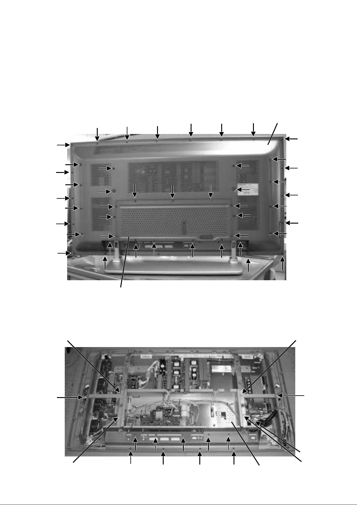
1-1: CABINET BACK/COVER BACK
1.
Remove the screw.
2.
Remove the Cabinet Back and Cover Back.
Cabinet Back
1-2: CHASSIS BLOCK
Disconnect the connector.
1.
Remove the screw.
2.
3.
Remove the Chassis Ass'y.
Cover Back
B1-1
Chassis Ass'y
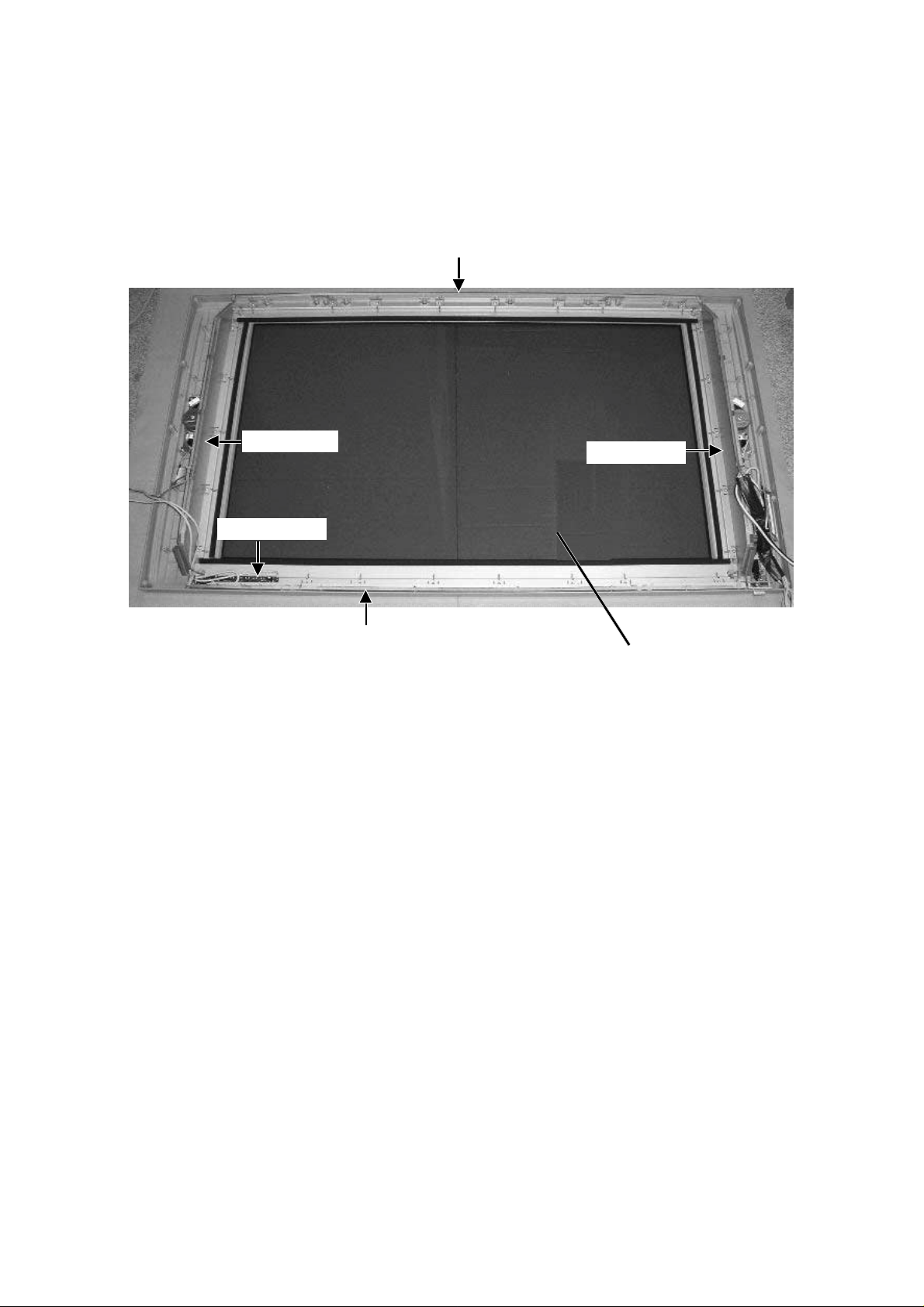
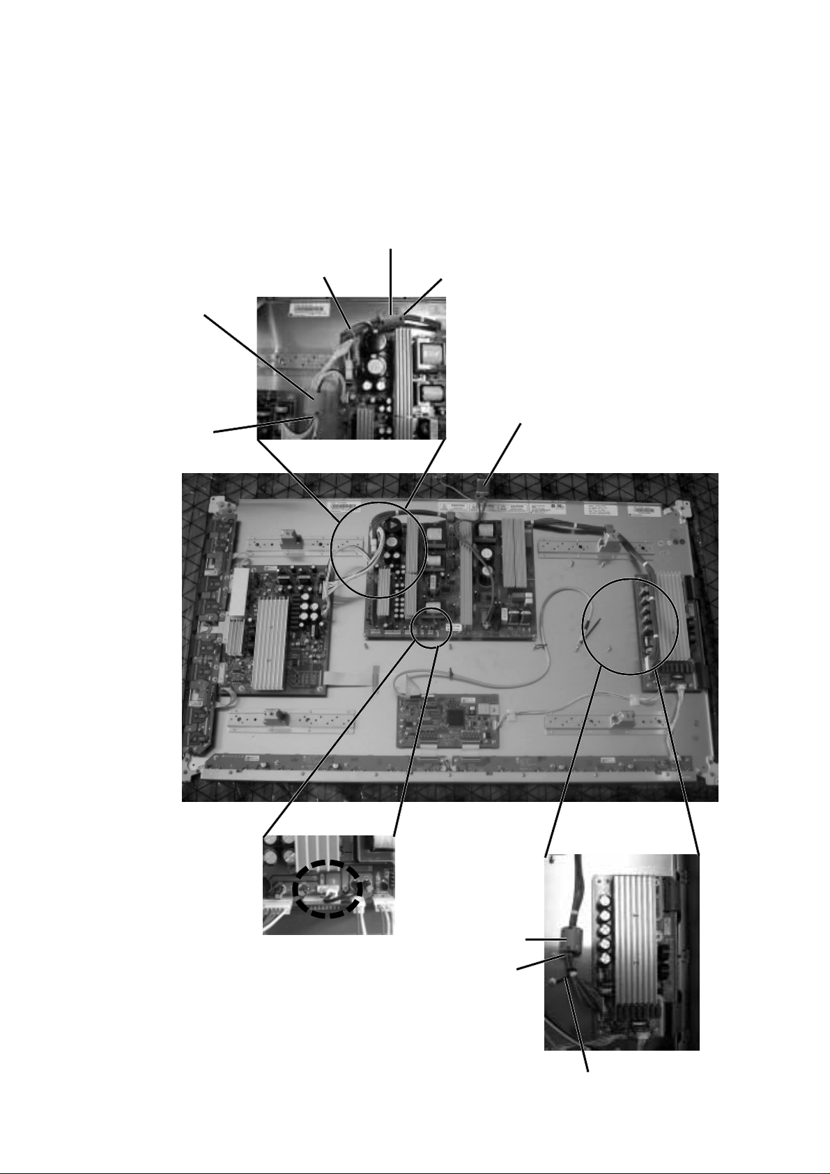
DISASSEMBLY INSTRUCTIONS
1-3: PDP MODULE
Remove the Tape.
1.
2.
Remove the screw.
Hold the Frame Main carefully and remove the PDP Module.
3.
NOTE
1.
When remove the PDP Module, raise the cushion carefully so that having a scratch on the face.
PDP Module
Frame Main
Frame Main
Raise the cushion.
B1-2
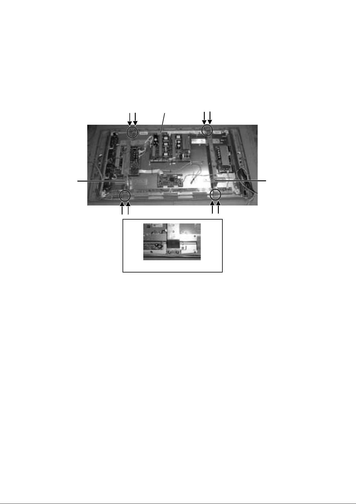
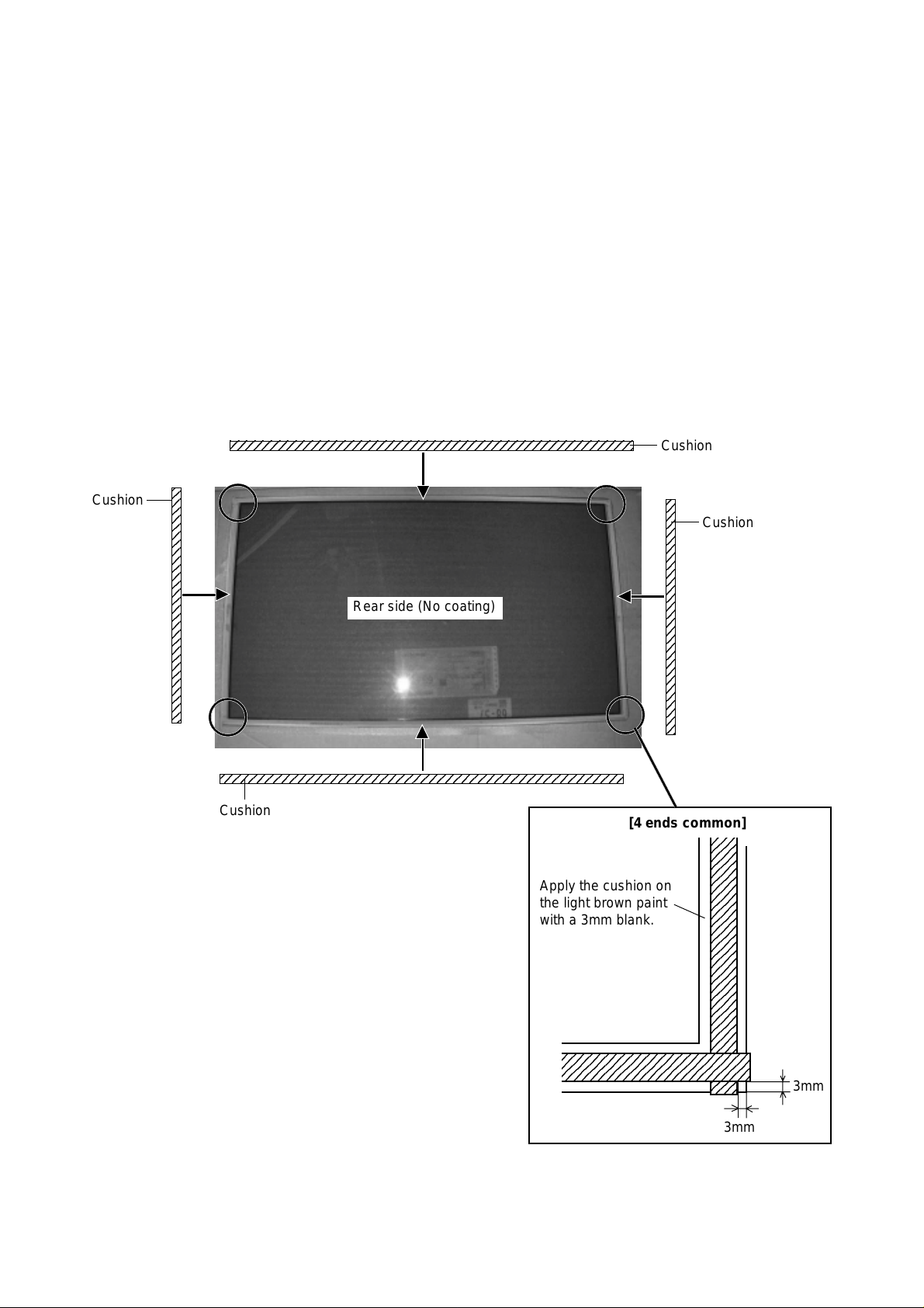
1-4: PDP FILTER
Remove the Operation PCB.
1.
2.
Remove the screw.
Remove the Shield Main.
3.
Remove the PDP Filter.
4.
DISASSEMBLY INSTRUCTIONS
Shield Main Top
Shield Main L
Operation PCB
Shield Main R
Shield Main Bottom
PDP Filter
B1-3
DISASSEMBLY INSTRUCTIONS
9
12345678901234567890123456789012123456789012345678
12345678901234567890123456789012123456789012345678
12
12
12
12
12
12
12
12
12
12
12
12
12
12
12
12
12
12
12
12
12
12
12
12
12
12
12
12
12
4
4
4
4
4
4
4
4
4
4
4
4
4
4
4
4
4
4
4
4
4
4
4
4
4
4
4
4
4
4
4
4
5
5
INSTALLATION METHOD OF PDP MODULE
NOTES FOR NEW PDP FILTER HANDLING
1.
When you handle the PDP Filter you mast wear the gloves twice, because, you are to avoid soiling it by your sweat and dust.
2.
When you lift the PDP Filter you put it between the palm of your hand. Don’t pick up it with your fingers.
3.
The back side of PDP Filter tends to set damaged. Since there is no coating. There fore, it put into the packing box at the
time of delivery, without piling up even at the time of unused. Also, when you take out it from a packing box, be careful of the
appearance which can not rub it.
4.
When the surface becomes dirty, be the cloth out of which it is soft and dust does not come, and as you draw a circle, wipe it.
When hard dirty, infiltrate ethanol etc. into cloth lightly and wipe. Don’t use ethanol for the back side.
5.
Do not apply it to direct sunshine so that the characteristic may change.
6.
When you inspect the scratch and the dirt, the air bubble of the PDP Filter surface that use the light.
1-5: PDP FILTER (PREPARATION)
Fix the Cusion. (Order the cushion newly.)1.
Cushion
Cushion
Cushion
Rear side (No coating)
2345678901234567890123456789012123456789012345678
Cushion
[4 ends common]
Apply the cushion on
the light brown paint
with a 3mm blank.
23456789012345678901234
23456789012345678901234
23
23
23
23
23
23
23
23
23
23
23
23
23
23
23
23
23
23
23
23
23
23
23
23
23
23
23
23
23
23
23
23
3mm
3mm
B1-4
DISASSEMBLY INSTRUCTIONS
NOTES FOR NEW PDP MODULE HANDLING
Do handling with the PDP Module by 2 persons.
1.
There is a step difference between the cover and PDP Module. So, when you remove the screws, place a cushion on it so
2.
that the PDP Module is not being scratched. Then remove the screws carefully.
When you remove the cover, do not scratch the FPC on both ends of PDP Module.
3.
Hold the four ends holder and be careful not to touch the glass area.
4.
Take care for the damage of vacuum exhaust pipe due to a collision.
5.
Moisture condensation may damage the PDP Module. So, leave it for 48 hours at the service room.
6.
Re-use the cover, vinyl sheet, and screws for returning of the PDP Module.
7.
Vacuum Exhaust Pipe
FPC
B1-5
DISASSEMBLY INSTRUCTIONS
1-6: PDP MODULE (PREPARATION)
Remove the fixing screw of Power PCB. Then fix the Wiring Clip. (Use the clipson defective PDP Module)
1.
Fix the Cord Clip. (Use the clip son defective PDP Module)
2.
Fix the Wiring Clip. (Use the clip son defective PDP Module)
3.
Wiring Clip
Cord Clip
B1-6
Cord Clip
45˚
Cord Clip
Wiring Clip
DISASSEMBLY INSTRUCTIONS
1-7: PDP MODULE (WIRING)
Fix the wiring with the Band Cord Clamp.
1.
Fix the Core Ferrite. (Use the clip son defective PDP Module)
2.
Remove the AC Inlet.
3.
Core Ferrite
Core Ferrite
Band Cord Clamp
Band Cord Clamp
Band Cord Clamp
AC Inlet
Set SW501 (24V)
Core Ferrite
Band Cord Clamp
Wiring Clip
B1-7
DISASSEMBLY INSTRUCTIONS
3
3
3
3
3
3
3
3
3
3
3
3
3
3
3
3
3
3
3
3
5
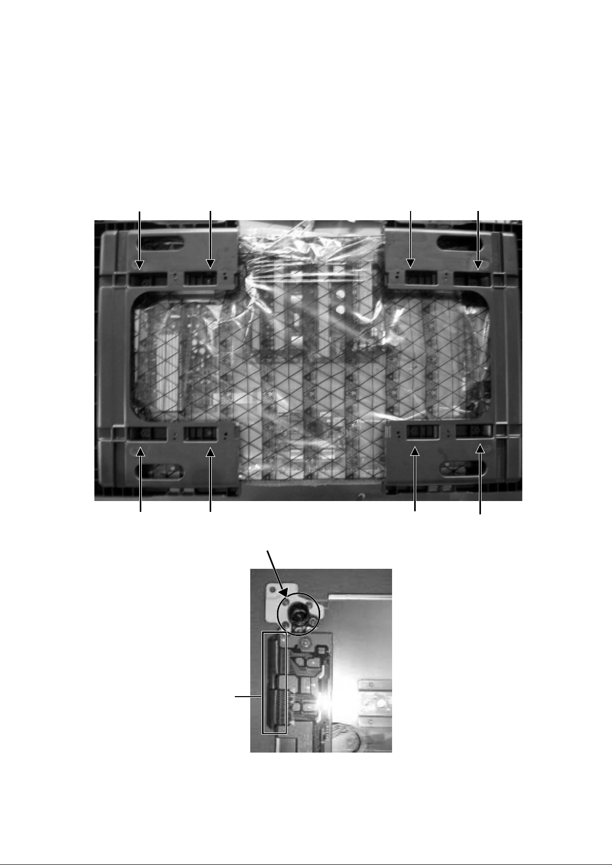
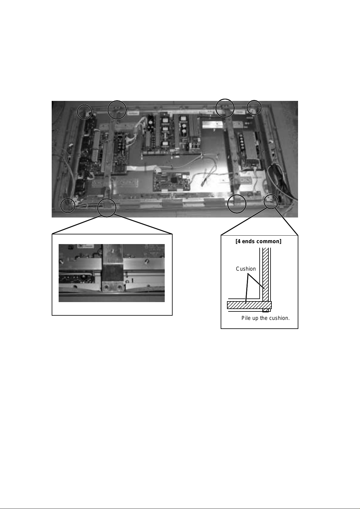
1-8: PDP MODULE
Fix the Frame Main. (Use the clip son defective PDP Module)
1.
Install the PDP Filter on the set.
2.
Install the Shield Main on the set.
3.
Hold the Frame Main carefully and install the New PDP Module on the set.
4.
[NG]
No mesh of the cushion (For all 4 positions)
[4 ends common]
Cushion
2345678901234
2
2
2
2
2
2
2
2
2
2
2
2
2
2
2
2
2
2
2
2
Pile up the cushion.
B1-8
DISASSEMBLY INSTRUCTIONS
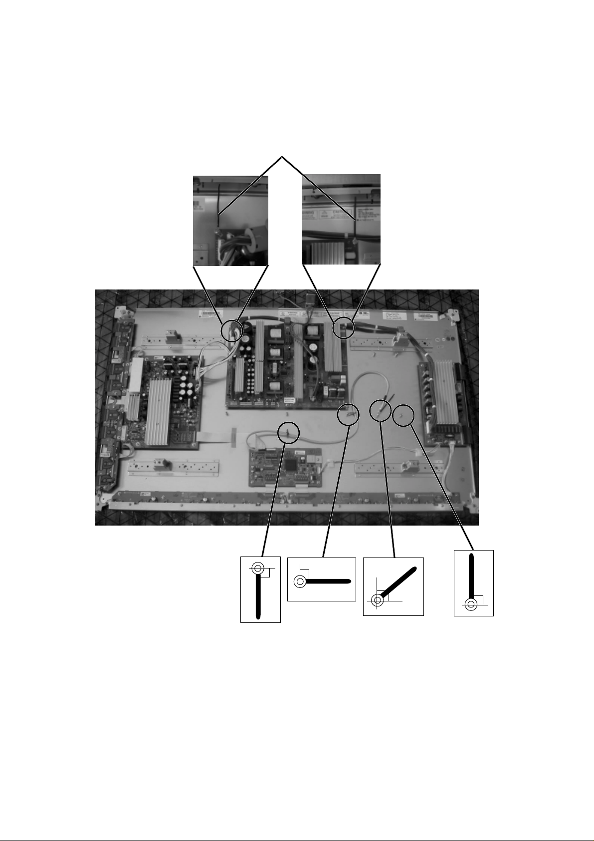
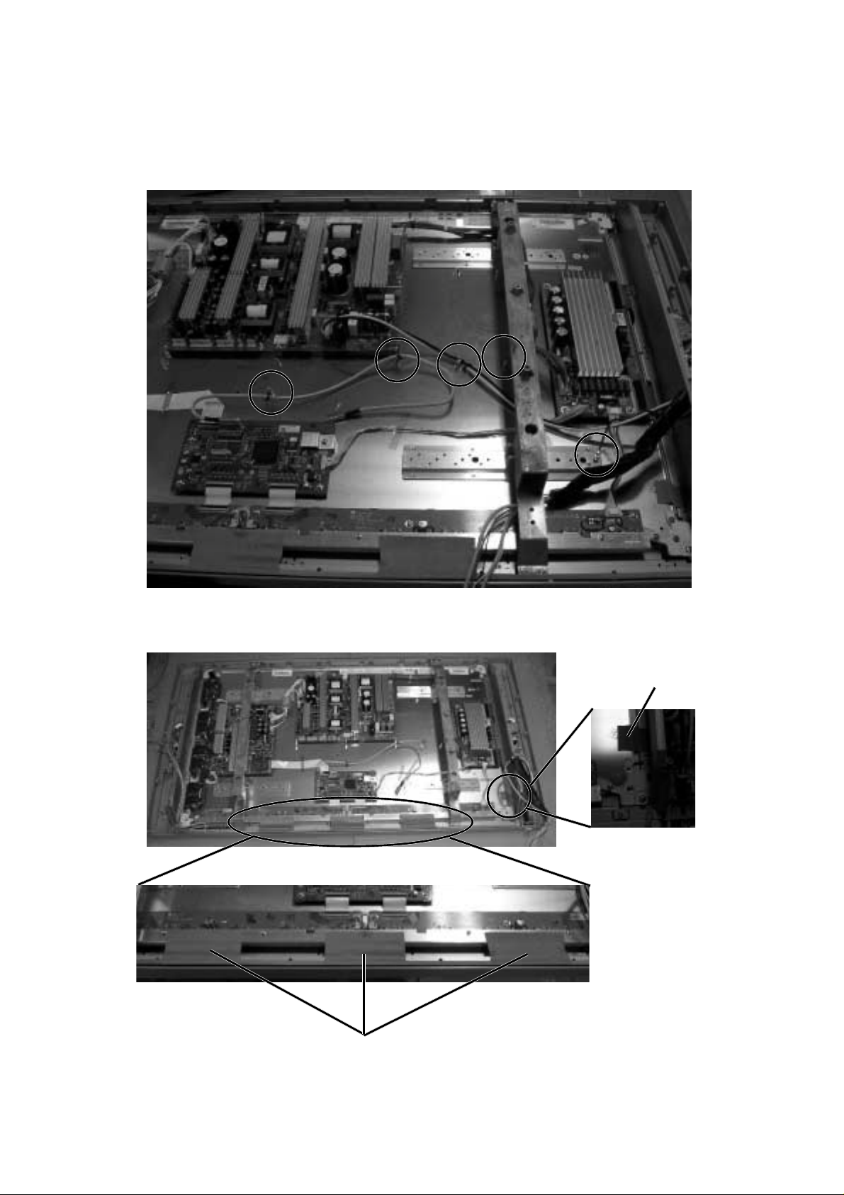
1-9: WIRE FIXING/TAPE
Do the wire fixing as shown the photo.
1.
2.
Stick the tapes on the position as shown the photo. (Order the tape newly.)
Tape
Tape
B1-9
DISASSEMBLY INSTRUCTIONS
1-10: CHASSIS BLOCK
Do the wire fixing as shown the photo, then install the Chassis Ass'y.
1.
Install the Stand Ass'y.
2.
Place the cable in
the Holder Cord.
Cord Clip
Sheet Earth Mark
Earth wire of
AC Inlet.
Place the cable in the
Holder Cord.
1-12: CABINET BACK/COVER BACK
1.
Check if the wire handlings are correct.
2.
Check if the cushion pastings are correct.
3.
Check if the tape pastings are correct.
4.
Install the Cabinet Back and Cover Back.
Place the cable in the
Holder Cord.
Toothed Lock Washer
Tie the wire around the PDP
Module post and then place
it in the Holder Cord.
B1-10
DISASSEMBLY INSTRUCTIONS
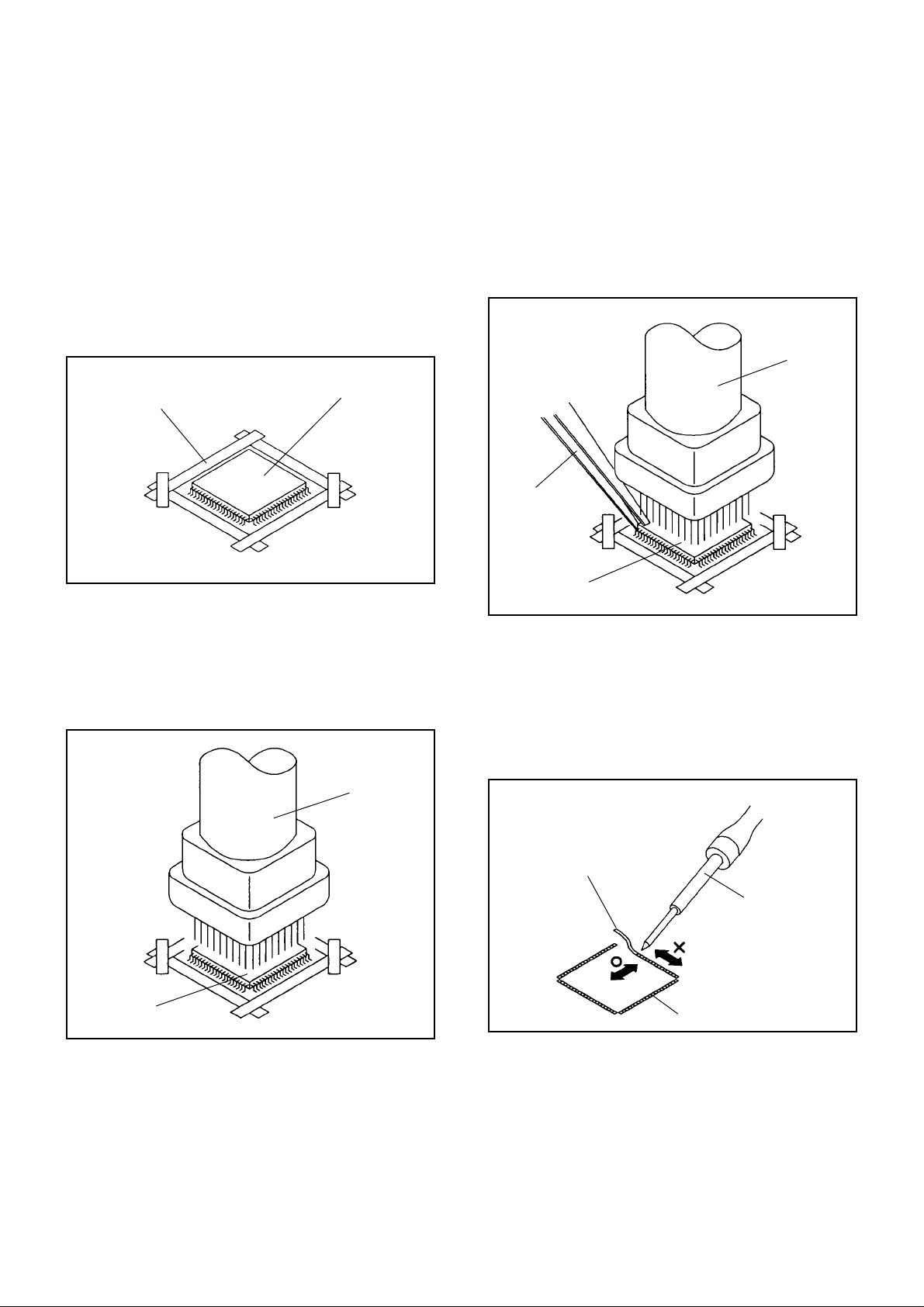
2.
REMOVAL AND INSTALLATION OF
FLAT PACKAGE IC
REMOVAL
Put Masking Tape (cotton tape) around the Flat Package
1.
IC to protect other parts from any damage.
(Refer to Fig. 2-1.)
NOTE
Masking is carried out on all the parts located within
10 mm distance from IC leads.
When IC starts moving back and forth easily after
3.
desoldering completely, pickup the corner of the IC using
tweezers and remove the IC by moving with the IC
desoldering machine. (Refer to Fig. 2-3.)
NOTE
Some ICs on the PCB are affixed with glue, so be
careful not to break or damage the foil of each IC
leads or solder lands under the IC when removing it.
Blower type IC
desoldering
machine
Masking Tape
(Cotton Tape)
Heat the IC leads using a blower type IC desoldering
2.
IC
machine. (Refer to Fig. 2-2.)
NOTE
Do not rotate or move the IC back and forth , until IC
can move back and forth easily after desoldering the
leads completely.
Blower type IC
desoldering machine
Fig. 2-1
Tweezers
IC
Peel off the Masking Tape.4.
Absorb the solder left on the pattern using the Braided
5.
Shield Wire. (Refer to Fig. 2-4.)
NOTE
Do not move the Braided Shield Wire in the vertical
direction towards the IC pattern.
Fig. 2-3
Braided Shield Wire
Soldering Iron
IC
Fig. 2-2
IC pattern
Fig. 2-4
B2-1

DISASSEMBLY INSTRUCTIONS
INSTALLATION
Take care of the polarity of new IC and then install the
1.
new IC fitting on the printed circuit pattern. Then solder
each lead on the diagonal positions of IC temporarily.
(Refer to Fig. 2-5.)
Soldering Iron
Solder temporarily
Supply the solder from the upper position of IC leads
2.
Solder temporarily
sliding to the lower position of the IC leads.
(Refer to Fig. 2-6.)
Fig. 2-5
When bridge-soldering between terminals and/or the
4.
soldering amount are not enough, resolder using a Thintip Soldering Iron. (Refer to Fig. 2-8.)
Thin-tip Soldering Iron
IC
Fig. 2-8
Finally, confirm the soldering status on four sides of the
5.
IC using a magnifying glass.
Confirm that no abnormality is found on the soldering
position and installation position of the parts around the
IC. If some abnormality is found, correct by resoldering.
NOTE
When the IC leads are bent during soldering and/or
repairing, do not repair the bending of leads. If the
bending of leads are repaired, the pattern may be
damaged. So, always be sure to replace the IC in this
case.
Soldering IronSolder
IC
Absorb the solder left on the lead using the Braided
3.
Supply soldering
from upper position
to lower position
Shield Wire. (Refer to Fig. 2-7.)
NOTE
Do not absorb the solder to excess.
Soldering Iron
IC
Braided Shield Wire
Fig. 2-6
Fig. 2-7
B2-2

SERVICE MODE LIST
This unit is provided with the following SERVICE MODES so you can repair, examine and adjust easily.
To enter to the SERVICE MODE function, press and hold both buttons simultaneously on the main unit and on the remote
control for more than the standard time in the appropriate condition. (See below chart.)
Set
Condition
TV mode
TV mode
TV mode
ALL mode
Set Key Operations
VOL. DOWN
(Minimum)
VOL. DOWN
(Minimum)
VOL. DOWN
(Minimum)
VOL. DOWN
(Minimum)
Remocon
Key
0 2 sec.
1 2 sec.
6 2 sec.
9 2 sec.
Standard
Time
Reset the user setting items (PICTURE, VOLUME, LANGUAGE
and NICAM AUTO/OFF) to the initial state for delivery.
Initialization of factory TV data.
NOTE:
POWER ON total hours are displayed on the screen.
Refer to the "PREVENTIVE CHECKS AND SERVICE INTERVALS"
(CONFIRMATION OF HOURS USED).
Can be checked of the INITIAL DATA of MEMORY IC.
Refer to the "WHEN REPLACING EEPROM (MEMORY) IC".
Display of the Adjustment MENU on the screen.
Refer to the "ELECTRICAL ADJUSTMENT" (On-Screen Display
Adjustment).
If you set factory initialization, the memories are reset
such as the channel setting, and the POWER ON total
hours.
CONFIRMATION OF HOURS USED
POWER ON total hours can be checked on the screen. Total hours are displayed in 16 system of notation.
NOTE: If you set a factory initialization, the total hours is reset to "0".
1.
Turn on the POWER, and set to the TV mode.
2.
Set the VOLUME to minimum.
3.
Press both VOL. DOWN button on the set and Channel
button (6) on the remote control for more than 2 seconds.
4.
After the confirmation of using hours, turn off the power.
ADDRESS DATA
OEC7139A_072
INIT 0001 20
PDP ON 0010
FIG. 1
MICON Version
Initial setting content of MEMORY IC.
POWER ON total hours.
= (16 x 16 x 16 x thousands digit value)
+ (16 x 16 x hundreds digit value)
+ (16 x tens digit value)
+ (ones digit value)
C-1

WHEN REPLACING EEPROM (MEMORY) IC
If a service repair is undertaken where it has been required to change the MEMORY IC, the following steps should be taken to
ensure correct data settings while making reference to TABLE 1.
1.
Turn on the POWER, and set to the TV mode.
2.
Set the VOLUME to minimum.
3.
Press both VOL. DOWN button on the set and Channel button (6) on the remote control for more than 2 seconds.
ADDRESS and DATA should appear as FIG 1.
4.
ADDRESS is now selected and should "blink". Using the RIGHT/LEFT button on the remote, step through the ADDRESS
until required ADDRESS to be changed is reached.
5.
Press ENTER to select DATA. When DATA is selected, it will "blink".
6.
Again, step through the DATA using RIGHT/LEFT button until required DATA value has been selected.
7.
Pressing ENTER will take you back to ADDRESS for further selection if necessary.
8.
Repeat steps 4 to 7 until all data has been checked.
9.
When satisfied correct DATA has been entered, turn POWER off (return to STANDBY MODE) to finish DATA input.
After the data input, set to the initializing of shipping.
10.
Turn on the POWER, and set to the TV mode.
11.
Press both VOL. DOWN button on the set and Channel button (1) on the remote control for more than 2 seconds.
12.
After the finishing of the initializing of shipping, the unit will turn off automatically.
The unit will now have the correct DATA for the new MEMORY IC.
ADDRESS DATA
OEC7139A_072
INIT 0001 20
PDP ON 0010
FIG. 1
INI +0 +1 +2 +3 +4 +5 +6 +7 +8 +9 +A +B +C +D +E + F
0000
0010
0020
0030
0040
0050
0060
0070
0080
0090
00A0
00B0
00C0
00D0
00E0
00F0
20 00 E4 79 7C 02 C0 08 9E FE F3 F3 90 80 31
00 20 00 00 AA 30 30 10 01 00 0E 48 05 03 4F 88
70 20 40 20 1E 70 4D 05 0B 35 00 04 F0 F0 E8 F0
FA 27 33 00 00 10 30 3B F8 08 16 41 4B 98 00 18
00 00 76 EA DB DB FA 00 47 00 00 15 10 00 10 0D
05 70 33 03 1F 24 F8 EF DB DB DB 03 00 00 22 00
00 22 00 00 20 00 01 FE 8B 93 82 8A FE FF 37 44
45 4F 51 53 59 5E 5F 61 62 64 66 67 68 69 6A 6B
6C 6D 6E 6E 6F 6F 70 70 71 71 72 72 73 73 74 74
75 75 76 76 77 77 78 78 79 79 7A 7A 7B 7B 7C 7C
37 44 45 4F 51 53 59 5E 5F 61 62 64 66 67 68 69
6A 6B 6C 6D 6E 6E 6F 6F 70 70 71 71 72 72 73 73
74 74 75 75 76 76 77 77 78 78 79 79 7A 7A 7B 7B
7C 7C DB DB A1 DB EA 0F 08 00 01 00 2C 13 74 6B
A6 D4 C1 3C F6 8C 84 84 00 82 00 85 00 00 73 25
CE F0 05 F0 05 07 A4 07 25 09 2A 09 68 F8 14 06
Table 1-1
C-2

WHEN REPLACING EEPROM (MEMORY) IC
INI +0 +1 +2 +3 +4 +5 +6 +7 +8 +9 +A +B +C +D +E + F
0600 31 F0 28 1F 08 08 20 80 80 80 7F 7F 7F F2 6E 80
0610 20 04 04 02 00 00 00 00 01 00 00 00 00 00 00 00
0620
0630
0640
0650
0660
0670
0680
0690
06A0
06B0
06C0
06D0
06E0
06F0
0700
0710
0720
0730
0740
0750
0760
0770
0780
0790
07A0
07B0
07C0
07D0
07E0~
07F0
38 30 20 FF 10 08 60 80 80 80 7F 7F 7F F6 6E B8
00 04 04 02 00 00 00 00 01 00 00 00 00 00 00 00
41 F0 60 1F 08 08 20 80 80 80 7F 7F 7F F2 6E 80
20 04 04 02 00 00 00 00 01 00 00 00 00 00 00 00
53 F0 70 8F 08 08 20 80 80 80 7F 7F 7F F2 6E 80
20 04 04 02 00 00 00 00 01 00 00 00 00 00 00 00
67 F0 A0 6F 10 08 60 80 80 80 7F 7F 7F F2 6E B8
28 04 04 02 00 00 00 00 01 00 00 00 00 00 00 00
67 F0 A0 F3 10 08 60 80 80 80 7F 7F 7F F2 6E B8
28 04 04 02 00 00 00 00 01 00 00 00 00 00 00 00
6B 30 18 F0 07 14 44 80 D0 80 80 7A 7F 6F 66 B5
30 0B 0F 02 00 00 00 00 01 00 00 00 00 00 00 00
35 90 18 70 07 14 35 80 D0 80 80 7A 80 6F 66 B5
30 0B 0F 02 00 00 00 00 01 00 00 00 00 00 00 00
67 10 88 B0 30 14 C0 80 D0 80 80 7A 80 6F 66 B5
20 0B 0F 02 00 00 00 00 01 00 00 00 00 00 00 00
89 70 A8 B0 30 05 94 80 D0 80 7F 7A 7E 6B 66 B5
30 0B 0F 02 00 00 00 00 01 00 00 00 00 00 00 00
42 F0 30 E5 08 08 20 80 80 80 7F 7F 7F F2 6E 80
20 04 0F 02 00 00 00 00 01 00 00 00 00 00 00 00
6B F0 18 70 07 14 44 80 D0 80 80 7A 80 6F 66 B5
30 0B 0F 02 00 00 00 01 00 00 00 00 00 00 00 00
35 F0 18 70 07 14 35 80 D0 80 80 7A 80 6F 66 B5
30 0B 0F 02 00 00 00 01 00 00 00 00 00 00 00 00
7B B0 A8 B0 2B 05 B0 80 D0 80 7F 7A 7E 6F 66 B5
20 0B 0F 02 00 00 00 01 00 00 00 00 00 00 00 00
A4 F0 A8 B0 30 05 94 80 D0 80 7F 7A 7D 6B 66 B5
30 0B 0F 02 00 00 00 01 00 00 00 00 00 00 00 00
FF FF FF FF FF FF FF FF FF FF FF FF FF FF FF FF
Table 1-2
C-3

WHEN REPLACING EEPROM (MEMORY) IC
INI +0 +1 +2 +3 +4 +5 +6 +7 +8 +9 +A +B +C +D +E + F
1000
1010
1020
1030
1040~
10B0
3F 02 18 FF 4C 33 65 6D CA 52 18 F7 4C 33 4C 29
00 00 00 00 00 00 00 00 00 00 00 00 00 00 00 00
7F 12 18 6B 83 7F F9 5E 7F 12 18 6B 83 7F F9 5E
7F 12 18 6B 83 7F F9 5E 7F 12 18 6B 83 7F F9 5E
00 00 00 00 00 00 00 00 00 00 00 00 00 00 00 00
10C0
10D0
10E0
10F0
1100
1110
1120
1130
1140
1150
1160
1170
1180
1190
11A0
11B0
11C0
11D0
11E0
11F0
1200
1210
1220
1230
1240
1250
1260
1270
1280
1290
01 00 02 00 00 00 04 00 05 00 00 00 00 00 00 00
00 00 00 00 00 00 00 00 00 00 00 00 00 00 00 00
20 00 04 00 02 00 04 00 20 3C 02 00 3C 00 50 00
B4 00 C8 00 2E 00 54 03 98 01 30 02 19 40 0A 11
04 01 00 00 04 00 00 00 04 02 C8 3C 37 00 04 00
B4 20 00 00 04 00 00 00 04 00 32 06 80 00 00 00
50 00 F0 C8 00 00 60 00 80 00 54 00 39 00 86 01
20 00 04 00 02 00 04 00 20 3C 02 00 3C 00 50 00
B4 00 C8 00 2E 00 54 03 98 01 30 02 19 40 0A 11
04 01 00 00 04 00 00 00 04 02 C8 3C 37 00 04 00
96 20 00 00 04 00 00 00 04 00 32 06 80 00 00 00
50 00 F0 B4 00 00 30 00 40 00 54 00 39 00 86 01
20 00 04 00 02 00 04 00 20 3C 02 00 3C 00 50 00
B4 00 C8 00 2E 00 54 03 54 01 30 02 19 40 0A 11
04 01 00 00 04 00 00 00 04 02 C8 3C 37 00 04 00
96 20 00 00 04 00 00 00 04 00 32 06 80 00 00 00
50 00 F0 B4 00 00 30 00 40 00 3F 00 39 00 86 01
20 00 04 00 02 00 04 00 20 3C 02 00 3C 00 50 00
B4 00 C8 00 2E 00 54 03 98 01 30 02 19 40 0A 11
04 01 00 00 04 00 00 00 04 02 C8 3C 37 00 04 00
96 20 00 00 04 00 00 00 04 00 32 06 80 00 00 00
50 00 F0 B4 00 00 30 00 40 00 54 00 39 00 86 01
20 00 04 00 02 00 04 00 20 3C 02 00 3C 00 50 00
B4 00 C8 00 2E 00 54 03 98 01 30 02 19 40 0A 11
04 01 00 00 04 00 00 00 04 02 C8 3C 37 00 04 00
96 20 00 00 04 00 00 00 04 00 32 06 80 00 00 00
50 00 F0 B4 00 00 30 00 40 00 54 00 39 00 86 01
20 00 04 00 02 00 04 00 20 3C 02 00 3C 00 50 00
B4 00 C8 00 2E 00 54 03 54 01 30 02 19 40 0A 11
04 01 00 00 04 00 00 00 04 02 C8 3C 37 00 04 00
Table 1-3
C-4

WHEN REPLACING EEPROM (MEMORY) IC
INI +0 +1 +2 +3 +4 +5 +6 +7 +8 +9 +A +B +C +D +E + F
12A0
12B0
12C0
12D0
12E0
12F0
1300
1310
1320
1330
1340
1350
1360
1370
1380
1390
13A0
13B0
13C0
13D0
13E0
13F0
1400
1410
1420
1430
1440
1450
1460
1470
1480
1490
96 20 00 00 04 00 00 00 04 00 32 06 80 00 00 00
50 00 F0 B4 00 00 30 00 40 00 3F 00 39 00 86 01
16 00 02 00 02 00 00 02 0A 11 00 01 00 00 2A 00
59 00 59 00 2E 00 54 03 98 01 30 02 18 30 0A 11
01 01 41 0E 02 00 00 05 04 04 41 0E 1C 00 02 0B
41 05 00 00 02 00 00 00 02 00 32 06 80 00 00 00
41 00 41 41 00 00 3C 00 6E 00 54 00 39 00 86 01
16 00 02 00 02 00 00 02 0A 11 00 01 00 00 2A 00
59 00 59 00 2E 00 54 03 98 01 30 02 18 30 0A 11
01 01 41 0E 02 00 00 05 04 04 41 0E 1C 00 02 0B
41 05 00 00 02 00 00 00 02 00 32 06 80 00 00 00
41 00 41 41 00 00 3C 00 6E 00 54 00 39 00 86 01
2C 00 02 00 02 00 00 02 16 16 00 01 46 00 46 00
46 00 46 00 2E 00 54 03 54 01 30 02 18 30 0A 11
01 01 41 0E 02 00 00 05 04 04 41 0E 1C 00 02 0B
41 05 00 00 02 00 00 00 02 00 32 06 80 00 00 00
41 00 41 41 00 00 3C 00 6E 00 3F 00 39 00 86 01
20 00 04 00 02 00 04 00 20 3C 02 00 3C 00 50 00
B4 00 C8 00 2E 00 54 03 98 01 30 02 19 40 0A 11
04 01 00 00 04 00 00 00 04 02 C8 3C 37 00 04 00
96 20 00 00 04 00 00 00 04 00 32 06 80 00 00 00
50 00 F0 B4 00 00 30 00 40 00 54 00 39 00 86 01
20 00 04 00 02 00 04 00 20 3C 02 00 3C 00 50 00
B4 00 C8 00 2E 00 54 03 98 01 30 02 19 40 0A 11
04 01 00 00 04 00 00 00 04 02 C8 3C 37 00 04 00
96 20 00 00 04 00 00 00 04 00 32 06 80 00 00 00
50 00 F0 B4 00 00 30 00 40 00 54 00 39 00 86 01
20 00 04 00 02 00 04 00 20 3C 02 00 3C 00 50 00
B4 00 C8 00 2E 00 54 03 54 01 30 02 19 40 0A 11
04 01 00 00 04 00 00 00 04 02 C8 3C 37 00 04 00
96 20 00 00 04 00 00 00 04 00 32 06 80 00 00 00
50 00 F0 B4 00 00 30 00 40 00 3F 00 39 00 86 01
Table 1-4
C-5

WHEN REPLACING EEPROM (MEMORY) IC
INI +0 +1 +2 +3 +4 +5 +6 +7 +8 +9 +A +B +C +D +E + F
14A0
14B0
14C0
14D0
14E0
14F0
1500
1510
1520
1530
1540
1550
1560
1570
1580
1590
15A0
15B0
15C0
15D0
15E0
15F0
1600
1610
1620
1630
1640
1650
1660
1670
1680
1690
20 00 04 00 02 00 04 00 20 3C 02 00 3C 00 50 00
B4 00 C8 00 2E 00 54 03 7C 01 30 02 19 40 0A 11
04 01 00 00 04 00 00 00 04 02 C8 3C 37 00 04 00
96 20 00 00 04 00 00 00 04 00 35 06 80 00 00 00
50 00 F0 B4 00 00 30 00 40 00 78 00 32 00 86 01
20 00 04 04 02 00 04 00 20 3C 04 04 3C 00 50 00
B4 00 C8 00 2E 00 54 03 98 01 30 02 19 40 0A 11
04 01 00 00 04 00 00 00 04 02 C8 3C 37 00 04 00
96 20 00 00 04 00 00 00 04 00 36 06 80 00 00 00
50 00 F0 B4 00 00 30 00 40 00 73 00 32 00 86 01
20 00 00 00 02 00 04 00 20 3C 00 00 3C 00 50 00
B4 00 C8 00 2E 00 54 03 E6 01 DC 03 19 40 0A 11
04 01 00 00 04 00 00 00 00 00 C8 3C 37 00 00 00
96 20 00 00 04 00 00 00 04 00 37 06 80 00 00 00
50 00 F0 B4 00 00 30 00 40 00 80 00 64 00 86 01
20 00 00 00 02 00 04 00 20 3C 00 00 3C 00 50 00
B4 00 C8 00 2E 00 54 03 74 01 16 06 19 40 0A 11
04 01 00 00 04 00 00 00 00 00 C8 3C 37 00 00 00
96 20 00 00 04 00 00 00 04 00 38 06 80 00 00 00
50 00 F0 B4 00 00 30 00 40 00 57 00 6E 00 86 01
20 00 04 00 02 00 04 00 20 3C 02 00 3C 00 50 00
B4 00 C8 00 2E 00 54 03 54 01 2A 02 19 40 0A 11
04 01 00 00 04 00 00 00 04 02 C8 3C 37 00 04 00
96 20 00 00 04 00 00 00 04 00 36 06 80 00 00 00
50 00 F0 B4 00 00 30 00 40 00 50 00 3C 00 86 01
20 00 04 00 02 00 04 00 20 3C 02 00 3C 00 50 00
B4 00 C8 00 2E 00 54 03 2E 01 12 02 19 40 0A 11
04 01 00 00 04 00 00 00 04 02 C8 3C 37 00 04 00
96 20 00 00 04 00 00 00 04 00 36 06 80 00 00 00
50 00 F0 B4 00 00 30 00 40 00 6A 00 46 00 86 01
20 00 00 00 02 00 04 00 20 3C 00 00 3C 00 50 00
B4 00 C8 00 2E 00 54 03 F2 01 12 04 19 40 0A 11
Table 1-5
C-6

WHEN REPLACING EEPROM (MEMORY) IC
INI +0 +1 +2 +3 +4 +5 +6 +7 +8 +9 +A +B +C +D +E + F
16A0
16B0
16C0
16D0
16E0
16F0
1700
1710
1720
1730
1740
1750
1760
1770
1780
1790
17A0
17B0
17C0
17D0
17E0
17F0
1800
1810
1820
1830
1840
1850
1860
1870
1880
1890
04 01 00 00 04 00 00 00 00 00 C8 3C 37 00 00 00
96 20 00 00 04 00 00 00 04 00 37 06 80 00 00 00
50 00 F0 B4 00 00 30 00 40 00 7C 00 4A 00 86 01
20 00 00 00 02 00 04 00 20 3C 00 00 3C 00 50 00
B4 00 C8 00 2E 00 54 03 62 01 FE 05 19 40 0A 11
04 01 00 00 04 00 00 00 00 00 C8 3C 37 00 00 00
96 20 00 00 04 00 00 00 04 00 38 06 80 00 00 00
50 00 F0 B4 00 00 30 00 40 00 60 00 7E 00 86 01
EC 81 2D 01 0E 00 34 08 05 08 07 00 01 00 00 00
80 00 54 03 6A 0C 2B 0B 65 0B 8F 0B F8 0B 42 0C
35 0D 42 0E 42 0E 34 05 32 00 54 03 E0 01 32 00
54 03 E2 01 18 04 73 02 01 00 1E 12 0D 00 1E C0
54 00 00 80 00 10 76 00 9E 02 3C 05 0A 00 61 AB
04 D2 2C 55 38 05 12 00 A2 00 2C 01 00 98 10 04
00 00 00 00 00 00 00 00 00 00 00 00 00 00 00 00
EC 81 2D 01 0E 00 34 08 05 08 07 00 01 00 00 00
80 00 80 02 00 10 2B 0B 65 0B 8F 0B F8 0B 42 0C
35 0D 42 0E 42 0E 34 05 9C 00 54 03 E0 01 32 00
54 03 E2 01 18 04 73 02 01 00 1E 12 0D 00 1E C0
54 00 00 80 7A 0F 76 00 9E 02 3C 05 0A 00 61 AB
04 D2 2C 55 38 05 12 00 A2 00 2C 01 00 98 10 04
00 00 00 00 00 00 00 00 00 00 00 00 00 00 00 00
EC 81 2D 01 0E 00 34 08 05 08 07 00 01 00 00 00
80 00 EA 02 4E 0E 2B 0B 65 0B 8F 0B F8 0B 42 0C
35 0D 42 0E 42 0E 34 05 67 00 54 03 E0 01 32 00
54 03 E2 01 18 04 73 02 01 00 1E 12 0D 00 1E C0
54 00 00 80 00 10 76 00 9E 02 3C 05 0A 00 61 AB
04 D2 2C 55 38 05 12 00 A2 00 2C 01 00 98 10 04
00 00 00 00 00 00 00 00 00 00 00 00 00 00 00 00
EC 81 2D 01 0E 00 34 08 05 08 07 00 01 00 00 00
80 80 54 03 87 0C 0D 0B 47 0B 71 0B DA 0B 24 0C
35 0D 42 0E 42 0E 34 05 32 00 54 03 E0 01 32 00
Table 1-6
C-7

WHEN REPLACING EEPROM (MEMORY) IC
INI +0 +1 +2 +3 +4 +5 +6 +7 +8 +9 +A +B +C +D +E + F
18A0
18B0
18C0
18D0
18E0
18F0
1900
1910
1920
1930
1940
1950
1960
1970
1980
1990
19A0
19B0
19C0
19D0
19E0
19F0
1A00
1A10
1A20
1A30
1A40
1A50
1A60
1A70
1A80
1A90
54 03 E2 01 18 04 73 02 01 00 1E 12 0D 00 1E C0
54 00 00 80 00 10 76 00 9E 02 3C 05 0A 00 61 AB
04 D2 2C 55 38 05 14 00 A2 00 2C 01 00 98 10 04
00 00 00 00 00 00 00 00 00 00 00 00 00 00 00 00
EC 81 2D 01 0E 00 34 08 05 08 07 00 01 00 00 00
80 00 54 03 6A 0C 2B 0B 65 0B 8F 0B F8 0B 42 0C
35 0D 42 0E 42 0E 55 04 32 00 54 03 E0 01 32 00
54 03 E2 01 18 04 73 02 01 00 92 0D 0D 00 1E C0
54 00 00 80 00 10 76 00 9E 02 3C 05 14 00 A1 EC
04 D2 22 51 38 05 62 00 D1 00 22 01 00 98 10 04
00 00 00 00 00 00 00 00 00 00 00 00 00 00 00 00
EC 01 2D 01 0E 00 34 08 05 08 07 00 01 00 00 00
80 00 54 03 82 0C 2B 0B 65 0B 8F 0B F8 0B 42 0C
35 0D 42 0E 42 0E 34 05 32 00 54 03 E0 01 32 00
54 03 E2 01 18 04 73 02 01 00 1E 12 0D 00 1E C0
54 00 00 80 00 10 52 00 00 05 9E 02 0A 00 61 AB
04 D2 2C 55 48 05 12 00 2A 00 62 02 00 98 10 04
00 00 00 00 00 00 00 00 00 00 00 00 00 00 00 00
EC 01 2D 01 0E 00 34 08 05 08 07 00 01 00 00 00
80 00 80 02 00 10 2B 0B 65 0B 8F 0B F8 0B 42 0C
35 0D 42 0E 42 0E 34 05 9C 00 54 03 E0 01 32 00
54 03 E2 01 18 04 73 02 01 00 1E 12 0D 00 1E C0
54 00 00 80 77 0F 52 00 00 05 9E 02 0A 00 61 AB
04 D2 2C 55 48 05 12 00 2A 00 62 02 00 98 10 04
00 00 00 00 00 00 00 00 00 00 00 00 00 00 00 00
EC 01 2D 01 0E 00 34 08 05 08 07 00 01 00 00 00
80 00 EA 02 38 0E 2B 0B 65 0B 8F 0B F8 0B 42 0C
35 0D 42 0E 42 0E 34 05 67 00 54 03 E0 01 32 00
54 03 E2 01 18 04 73 02 01 00 1E 12 0D 00 1E C0
54 00 00 80 00 10 52 00 00 05 9E 02 0A 00 61 AB
04 D2 2C 55 48 05 12 00 2A 00 62 02 00 98 10 04
00 00 00 00 00 00 00 00 00 00 00 00 00 00 00 00
Table 1-7
C-8

WHEN REPLACING EEPROM (MEMORY) IC
INI +0 +1 +2 +3 +4 +5 +6 +7 +8 +9 +A +B +C +D +E + F
1AA0
1AB0
1AC0
1AD0
1AE0
1AF0
1B00
1B10
1B20
1B30
1B40
1B50
1B60
1B70
1B80
1B90
1BA0
1BB0
1BC0
1BD0
1BE0
1BF0
1C00
1C10
1C20
1C30
1C40
1C50
1C60
1C70
1C80
1C90
EC 01 2D 01 0E 00 34 08 05 08 07 00 01 00 00 00
80 80 54 03 82 0C 2B 0B 65 0B 8F 0B F8 0B 42 0C
35 0D 42 0E 42 0E 34 05 32 00 54 03 E0 01 32 00
54 03 E2 01 18 04 73 02 01 00 1E 12 0D 00 1E C0
54 00 00 80 00 10 52 00 00 05 9E 02 0A 00 61 AB
04 D2 2C 55 48 05 14 00 2A 00 62 02 00 98 10 04
00 00 00 00 00 00 00 00 00 00 00 00 00 00 00 00
EC 01 2D 01 0E 00 34 08 05 08 07 00 01 00 00 00
80 00 54 03 82 0C 2B 0B 65 0B 8F 0B F8 0B 42 0C
35 0D 42 0E 42 0E 55 04 32 00 54 03 E0 01 32 00
54 03 E2 01 18 04 73 02 01 00 92 0D 0D 00 1E C0
54 00 00 80 00 10 52 00 00 05 9E 02 22 00 A1 EC
04 D2 22 51 48 05 60 00 51 00 44 02 00 98 10 04
00 00 00 00 00 00 00 00 00 00 00 00 00 00 00 00
EC 01 2D 01 0E 00 34 08 05 08 07 00 01 00 00 00
80 00 54 03 00 10 2B 0B 65 0B 8F 0B F8 0B 42 0C
35 0D 42 0E 42 0E C8 04 32 00 54 03 E0 01 32 00
54 03 E2 01 40 04 0D 02 01 00 D2 16 0D 00 1E C0
54 00 00 80 7A 0B 52 00 CF 05 C4 04 0A 00 5F A9
04 D2 2C 55 48 05 E7 02 94 00 E4 02 00 A8 10 04
00 00 00 00 00 00 00 00 00 00 00 00 00 00 00 00
EC 01 2D 01 0E 00 34 08 05 08 07 00 01 00 00 00
80 00 54 03 00 10 2B 0B 65 0B 8F 0B F8 0B 42 0C
35 0D 42 0E 42 0E C8 04 32 00 54 03 E0 01 32 00
54 03 E2 01 40 04 0D 02 01 00 26 11 0D 00 0A C0
40 00 00 00 AD 07 AA 00 80 07 26 07 0A 00 5F A9
04 D2 2C 55 48 05 30 02 94 00 60 02 00 A8 08 04
00 00 00 00 00 00 00 00 00 00 00 00 00 00 00 00
EC 81 2D 01 0E 00 34 08 05 08 07 00 01 00 00 00
80 00 54 03 A6 0C 52 0B 8C 0B B6 0B 21 0C 6C 0C
63 0D 73 0E 73 0E 43 04 32 00 54 03 E0 01 32 00
54 03 E2 01 75 04 25 02 01 00 44 0F 0D 00 1E C0
Table 1-8
C-9

WHEN REPLACING EEPROM (MEMORY) IC
INI +0 +1 +2 +3 +4 +5 +6 +7 +8 +9 +A +B +C +D +E + F
1CA0
1CB0
1CC0
1CD0
1CE0
1CF0
1D00
1D10
1D20
1D30
1D40
1D50
1D60
1D70
1D80
1D90
1DA0
1DB0
1DC0
1DD0
1DE0
1DF0
1E00
1E10
1E20
1E30
1E40
1E50
1E60
1E70
1E80
1E90
54 00 00 80 00 10 76 00 A4 02 50 05 0A 00 21 AB
04 D2 F0 54 48 05 12 00 91 00 FA 00 00 98 10 04
00 00 00 00 00 00 00 00 00 00 00 00 00 00 00 00
EC 81 2D 01 0E 00 34 08 05 08 07 00 01 00 00 00
80 00 80 02 00 10 52 0B 8C 0B B6 0B 21 0C 6C 0C
63 0D 73 0E 73 0E 43 04 9C 00 54 03 E0 01 32 00
54 03 E2 01 75 04 25 02 01 00 44 0F 0D 00 1E C0
54 00 00 80 32 0F 76 00 A4 02 50 05 0A 00 21 AB
04 D2 F0 54 48 05 12 00 91 00 FA 00 00 98 10 04
00 00 00 00 00 00 00 00 00 00 00 00 00 00 00 00
EC 81 2D 01 0E 00 34 08 05 08 07 00 01 00 00 00
80 00 EA 02 A6 0E 52 0B 8C 0B B6 0B 21 0C 6C 0C
63 0D 73 0E 73 0E 43 04 67 00 54 03 E0 01 32 00
54 03 E2 01 75 04 25 02 01 00 44 0F 0D 00 1E C0
54 00 00 80 00 10 76 00 A4 02 50 05 0A 00 21 AB
04 D2 F0 54 48 05 12 00 91 00 FA 00 00 98 10 04
00 00 00 00 00 00 00 00 00 00 00 00 00 00 00 00
EC 81 2D 01 0E 00 34 08 05 08 07 00 01 00 00 00
80 80 54 03 AD 0C 3A 0B 80 0B A8 0B 1E 0C 68 0C
63 0D 73 0E 73 0E 5C 04 32 00 54 03 E0 01 32 00
54 03 E2 01 75 04 25 02 01 00 4D 0F 0D 00 1E C0
54 00 00 80 00 10 76 00 A4 02 50 05 0A 00 61 AB
04 D2 F2 40 48 05 11 00 91 00 FA 00 00 98 10 04
00 00 00 00 00 00 00 00 00 00 00 00 00 00 00 00
EC 81 2D 01 0E 00 34 08 05 08 07 00 01 00 00 00
80 00 54 03 A6 0C 52 0B 8C 0B B6 0B 21 0C 6C 0C
63 0D 73 0E 73 0E 39 04 32 00 A8 02 E0 01 32 00
54 03 E1 01 39 04 DC 02 01 00 6F 0B 0D 00 1E C0
54 00 00 80 00 10 74 00 A8 02 48 05 10 00 5E AD
04 D0 F2 40 48 05 52 00 7B 00 F2 00 00 98 10 04
00 00 00 00 00 00 00 00 00 00 00 00 00 00 00 00
EC 01 2D 01 0E 00 34 08 05 08 07 00 01 00 00 00
Table 1-9
C-10

WHEN REPLACING EEPROM (MEMORY) IC
INI +0 +1 +2 +3 +4 +5 +6 +7 +8 +9 +A +B +C +D +E + F
1EA0
1EB0
1EC0
1ED0
1EE0
1EF0
1F00
1F10
1F20
1F30
1F40
1F50
1F60
1F70
1F80
1F90
1FA0
1FB0
1FC0
1FD0
1FE0
1FF0
2000
2010
2020
2030
2040
2050
2060
2070
2080
2090
80 00 54 03 90 0C 52 0B 8C 0B B6 0B 21 0C 6C 0C
63 0D 73 0E 73 0E 43 04 32 00 54 03 E0 01 32 00
54 03 E2 01 63 04 25 02 01 00 44 0F 0D 00 1E C0
54 00 00 80 00 10 52 00 EE 02 A8 02 14 00 21 AB
04 D2 F0 54 48 05 11 00 91 00 F4 01 00 98 10 04
00 00 00 00 00 00 00 00 00 00 00 00 00 00 00 00
EC 01 2D 01 0E 00 34 08 05 08 07 00 01 00 00 00
80 00 80 02 00 10 52 0B 8C 0B B6 0B 21 0C 6C 0C
63 0D 73 0E 73 0E 43 04 9C 00 54 03 E0 01 32 00
54 03 E2 01 63 04 25 02 01 00 44 0F 0D 00 1E C0
54 00 00 80 4E 0F 52 00 EE 02 A8 02 14 00 21 AB
04 D2 F0 54 48 05 12 00 91 00 F4 01 00 98 10 04
00 00 00 00 00 00 00 00 00 00 00 00 00 00 00 00
EC 01 2D 01 0E 00 34 08 05 08 07 00 01 00 00 00
80 00 EA 02 56 0E 52 0B 8C 0B B6 0B 21 0C 6C 0C
63 0D 73 0E 73 0E 43 04 67 00 54 03 E0 01 32 00
54 03 E2 01 63 04 25 02 01 00 44 0F 0D 00 1E C0
54 00 00 80 00 10 52 00 EE 02 A8 02 14 00 21 AB
04 D2 F0 54 48 05 12 00 91 00 F4 01 00 98 10 04
00 00 00 00 00 00 00 00 00 00 00 00 00 00 00 00
EC 01 2D 01 0E 00 34 08 05 08 07 00 01 00 00 00
80 80 54 03 90 0C 52 0B 8C 0B B6 0B 21 0C 6C 0C
63 0D 73 0E 73 0E 5C 04 32 00 54 03 E0 01 32 00
54 03 E2 01 63 04 25 02 01 00 4D 0F 0D 00 1E C0
54 00 00 80 00 10 52 00 EE 02 A8 02 14 00 61 AB
04 D2 F0 54 48 05 11 00 91 00 F4 01 00 98 10 04
00 00 00 00 00 00 00 00 00 00 00 00 00 00 00 00
EC 01 2D 01 0E 00 34 08 05 08 07 00 01 00 00 00
80 00 54 03 90 0C 52 0B 8C 0B B6 0B 21 0C 6C 0C
63 0D 73 0E 73 0E 3C 04 32 00 54 03 E0 01 32 00
54 03 E2 01 63 04 25 02 01 00 6F 0B 0D 00 1E C0
54 00 00 80 00 10 52 00 EE 02 A8 02 22 00 5E AD
Table 1-10
C-11

WHEN REPLACING EEPROM (MEMORY) IC
INI +0 +1 +2 +3 +4 +5 +6 +7 +8 +9 +A +B +C +D +E + F
20A0
20B0
20C0
20D0
20E0
20F0
2100
2110
2120
2130
2140
2150
2160
2170
2180
2190
21A0
21B0
21C0
21D0
21E0
21F0
2200
2210
2220
2230
2240
2250
2260
2270
2280
2290
04 D2 F2 40 48 05 54 00 2E 00 E8 01 00 98 10 04
00 00 00 00 00 00 00 00 00 00 00 00 00 00 00 00
EC 01 2D 01 0E 00 34 08 05 08 07 00 01 00 00 00
80 00 54 03 00 10 52 0B 8C 0B B6 0B 21 0C 6C 0C
63 0D 73 0E 73 0E 73 04 32 00 54 03 E0 01 32 00
54 03 E2 01 63 04 25 02 01 00 CC 16 0D 00 1E C0
54 00 00 80 6D 0B 52 00 CF 05 C4 04 0A 00 21 AB
04 D2 F0 54 48 05 E4 02 23 00 D0 02 00 A8 10 04
00 00 00 00 00 00 00 00 00 00 00 00 00 00 00 00
EC 01 2D 01 0E 00 34 08 05 08 07 00 01 00 00 00
80 00 54 03 00 10 52 0B 8C 0B B6 0B 21 0C 6C 0C
A1 02 00 0E 73 0E 75 04 32 00 54 03 E0 01 32 00
54 03 E2 01 63 04 25 02 01 00 1F 11 0D 00 1E C0
54 00 00 00 A2 07 D2 00 70 07 98 08 0A 00 21 AB
04 D2 F0 54 48 05 2E 02 23 00 25 02 00 A8 08 04
00 00 00 00 00 00 00 00 00 00 00 00 00 00 00 00
EC 81 2D 01 0E 00 34 08 05 08 07 00 01 00 00 00
80 00 54 03 05 0C 52 0B 8C 0B B6 0B 21 0C 6C 0C
63 0D 73 0E 73 0E 10 04 32 00 80 02 E0 01 32 00
54 03 E1 01 18 04 73 02 01 00 00 10 0D 00 1E C0
54 00 00 00 00 10 76 00 A4 02 80 02 0A 00 21 AA
04 D2 E8 50 48 05 0A 00 48 00 12 02 00 A8 00 00
00 00 00 00 00 00 00 00 00 00 00 00 00 00 00 00
EC 81 2D 01 0E 00 34 08 05 08 07 00 01 00 00 00
80 00 80 02 00 10 52 0B 8C 0B B6 0B 21 0C 6C 0C
63 0D 73 0E 73 0E 10 04 9C 00 80 02 E0 01 32 00
54 03 E1 01 18 04 73 02 01 00 00 10 0D 00 1E C0
54 00 00 00 00 10 76 00 A4 02 80 02 0A 00 21 AA
04 D2 E8 50 48 05 0A 00 48 00 12 02 00 A8 00 00
00 00 00 00 00 00 00 00 00 00 00 00 00 00 00 00
EC 81 2D 01 0E 00 34 08 05 08 07 00 01 00 00 00
80 00 54 03 06 0F 52 0B 8C 0B B6 0B 21 0C 6C 0C
Table 1-11
C-12

WHEN REPLACING EEPROM (MEMORY) IC
INI +0 +1 +2 +3 +4 +5 +6 +7 +8 +9 +A +B +C +D +E + F
22A0
22B0
22C0
22D0
22E0
22F0
2300
2310
2320
2330
2340
2350
2360
2370
2380
2390
23A0
23B0
23C0
23D0
23E0
23F0
2400
2410
2420
2430
2440
2450
2460
2470
2480
2490
63 0D 73 0E 73 0E 37 04 32 00 20 03 E0 01 32 00
54 03 E1 01 18 04 73 02 01 00 00 14 0D 00 1E C0
54 00 00 00 00 10 76 00 A4 02 20 03 01 00 21 AA
04 D2 2C 55 48 05 0A 00 A2 00 2C 01 00 A8 00 00
00 00 00 00 00 00 00 00 00 00 00 00 00 00 00 00
EC 81 2D 01 0E 00 34 08 05 08 07 00 01 00 00 00
80 00 80 02 00 10 52 0B 8C 0B B6 0B 21 0C 6C 0C
63 0D 73 0E 73 0E 37 04 9C 00 20 03 E0 01 32 00
54 03 E1 01 18 04 73 02 01 00 00 14 0D 00 1E C0
54 00 00 00 CD 0C 76 00 A4 02 20 03 01 00 21 AA
04 D2 E8 50 48 05 0A 00 48 00 12 02 00 A8 00 00
00 00 00 00 00 00 00 00 00 00 00 00 00 00 00 00
EC 81 2D 01 0E 00 34 08 05 08 07 00 01 00 00 00
80 00 5E 03 EC 0F 52 0B 8C 0B B6 0B 21 0C 6C 0C
63 0D 73 0E 73 0E 1D 04 32 00 54 03 E0 01 32 00
54 03 E1 01 18 04 73 02 01 00 00 10 0D 00 1E C0
54 00 00 00 00 10 76 00 A4 01 50 03 09 00 21 AA
04 D2 E8 50 48 05 0A 00 C8 00 12 02 00 98 00 00
00 00 00 00 00 00 00 00 00 00 00 00 00 00 00 00
EC 81 2D 01 0E 00 34 08 05 08 07 00 01 00 00 00
80 00 80 02 00 10 52 0B 8C 0B B6 0B 21 0C 6C 0C
63 0D 73 0E 73 0E 39 04 9C 00 54 03 E0 01 32 00
54 03 E1 01 38 04 73 02 01 00 99 19 0D 00 1E C0
54 00 00 00 00 0A 76 00 A4 02 00 04 09 00 21 AA
04 D2 E8 50 48 05 0A 00 C9 00 32 03 00 A8 00 00
00 00 00 00 00 00 00 00 00 00 00 00 00 00 00 00
EC 81 2D 01 0E 00 34 08 05 08 07 00 01 00 00 00
80 00 54 03 06 0F 52 0B 8C 0B B6 0B 21 0C 6C 0C
63 0D 73 0E 73 0E 37 04 32 00 20 03 E0 01 32 00
54 03 E1 01 18 04 73 02 01 00 00 14 0D 00 1E C0
54 00 00 00 00 10 76 00 A4 02 20 03 01 00 21 AA
04 D2 E8 50 48 05 0A 00 F7 00 8A 02 00 A8 00 00
Table 1-12
C-13

WHEN REPLACING EEPROM (MEMORY) IC
INI +0 +1 +2 +3 +4 +5 +6 +7 +8 +9 +A +B +C +D +E + F
24A0
24B0
24C0
24D0
24E0
24F0
2500
2510
2520
2530
2540
2550
2560
2570
2580
2590
25A0
25B0
25C0
25D0
25E0
25F0
2600
2610
2620
2630
2640
2650
2660
2670
2680
2690
00 00 00 00 00 00 00 00 00 00 00 00 00 00 00 00
EC 81 2D 01 0E 00 34 08 05 08 07 00 01 00 00 00
80 00 80 02 00 10 52 0B 8C 0B B6 0B 21 0C 6C 0C
63 0D 73 0E 73 0E 37 04 9C 00 20 03 E0 01 32 00
54 03 E1 01 18 04 73 02 01 00 00 14 0D 00 1E C0
54 00 00 00 CD 0C 76 00 A4 02 20 03 01 00 21 AA
04 D2 E8 50 48 05 0A 00 F7 00 8A 02 00 A8 00 00
00 00 00 00 00 00 00 00 00 00 00 00 00 00 00 00
EC 81 2D 01 0E 00 34 08 05 08 07 00 01 00 00 00
80 00 54 03 00 10 52 0B 8C 0B B6 0B 21 0C 6C 0C
63 0D 73 0E 73 0E 39 04 32 00 54 03 E0 01 32 00
54 03 E1 01 18 04 73 02 01 00 99 19 0D 00 1E C0
54 00 00 00 50 0D 76 00 A4 02 00 04 09 00 21 AA
04 D2 E8 50 48 05 0A 00 C9 00 32 03 00 A8 00 00
00 00 00 00 00 00 00 00 00 00 00 00 00 00 00 00
EC 81 2D 01 0E 00 34 08 05 08 07 00 01 00 00 00
80 00 80 02 00 10 52 0B 8C 0B B6 0B 21 0C 6C 0C
63 0D 73 0E 73 0E 39 04 9C 00 54 03 E0 01 32 00
54 03 E1 01 18 04 73 02 01 00 99 19 0D 00 1E C0
54 00 00 00 00 0A 76 00 A4 02 00 04 09 00 21 AA
04 D2 E8 50 48 05 0A 00 C9 00 32 03 00 A8 00 00
00 00 00 00 00 00 00 00 00 00 00 00 00 00 00 00
EC 81 2D 01 0E 00 34 08 05 08 07 00 01 00 00 00
80 00 54 03 00 10 52 0B 8C 0B B6 0B 21 0C 6C 0C
63 0D 73 0E 73 0E 47 04 32 00 54 03 E0 01 32 00
54 03 E1 01 18 04 73 02 01 00 00 18 0D 00 1E C0
54 00 00 00 A6 0A 76 00 A4 02 00 05 00 00 21 AA
04 D2 E8 50 48 05 0A 00 97 00 02 03 00 A8 00 00
00 00 00 00 00 00 00 00 00 00 00 00 00 00 00 00
24 02 32 01 22 08 40 08 10 00 0F 00 01 08 00 00
F0 03 54 03 00 10 1E 0C 10 0D 22 0E 43 0F B6 0F
CD 11 3A 13 C4 14 49 04 32 00 54 03 E0 01 32 00
Table 1-13
C-14

WHEN REPLACING EEPROM (MEMORY) IC
INI +0 +1 +2 +3 +4 +5 +6 +7 +8 +9 +A +B +C +D +E + F
26A0
26B0
26C0
26D0
26E0
26F0
2700
2710
2720
2730
2740
2750
2760
2770
2780
2790
27A0
27B0
27C0
27D0
27E0
27F0
2800
2810
2820
2830
2840
2850
2860
2870
2880
2890
54 03 E1 01 47 04 F1 01 8A C0 9A 19 09 00 0A C0
40 00 00 00 A6 0A C8 00 80 07 00 05 1A 00 21 AA
04 D2 E8 50 48 05 0A 00 36 00 02 03 0F 90 00 00
00 00 00 00 00 00 00 00 00 00 00 00 00 00 00 00
96 0F 00 59 C8 93 92 24 C0 C2 F2 0A 8E 8E 19 36
00 30 A0 1B 04 A0 04 04 C8 00 00 C4 00 00 06 00
F8 08 6E CA 1E AC 00 02 10 42 04 C4 0C 40 0C 10
08 6C 00 CC A1 38 02 00 EE 04 20 03 00 00 00 00
00 00 00 00 00 00 00 00 00 00 00 00 00 00 00 00
96 0F 00 59 C8 93 92 24 C0 C2 F2 0A 8E 8E 19 36
C0 3F A0 1B 04 A0 04 04 C8 00 00 C4 00 00 06 00
F8 08 6E CA 1E AC 00 02 10 42 02 44 0C 40 0C 10
08 6C 00 C0 A1 38 02 00 EE 04 20 01 00 00 00 00
00 00 00 00 00 00 00 00 00 00 00 00 00 00 00 00
96 0F 00 59 C8 93 92 24 B4 C2 E6 0A 82 8E 19 36
00 30 A0 1B 04 A0 04 04 C8 00 00 C4 00 00 06 00
EC 08 6E CA 0A AC 00 23 10 82 04 84 18 40 18 10
08 2C 00 0C E2 38 00 00 EE 04 20 01 00 00 00 00
00 00 00 00 00 00 00 00 00 00 00 00 00 00 00 00
96 0F 00 59 C8 B3 92 24 C0 C2 F2 0A 8E 8E 19 36
00 30 A0 1B 04 A0 04 04 C8 00 00 C4 00 00 06 00
F8 08 6E CA 1E AC 00 02 10 42 04 C4 0C 40 0C 10
08 6C 00 CC A1 38 02 00 EE 04 20 03 00 00 00 00
00 00 00 00 00 00 00 00 00 00 00 00 00 00 00 00
96 0F 00 59 C8 B3 92 24 C0 C2 F2 0A 8E 8E 19 36
C0 3F A0 1B 04 A0 04 04 C8 00 00 C4 00 00 66 01
F8 08 6E CA 1E AC 00 02 10 42 02 44 0C 40 0C 10
08 6C 00 C0 A1 38 02 00 EE 04 20 01 00 00 00 00
00 00 00 00 00 00 00 00 00 00 00 00 00 00 00 00
96 0F 00 59 C8 B3 92 24 B4 C2 E6 0A 82 8E 19 36
00 30 A0 1B 04 A0 04 04 C8 00 00 C4 00 00 06 00
EC 08 6E CA 0A AC 00 23 10 82 04 84 18 40 18 10
Table 1-14
C-15

WHEN REPLACING EEPROM (MEMORY) IC
INI +0 +1 +2 +3 +4 +5 +6 +7 +8 +9 +A +B +C +D +E + F
28A0
28B0
28C0
28D0
28E0
28F0
2900
2910
2920
2930
2940
2950
2960
2970
2980
2990
29A0
29B0
29C0
29D0
29E0
29F0
2A00
2A10
2A20
2A30
2A40
2A50
2A60
2A70
2A80
2A90
08 2C 00 0C 61 38 08 00 2E 17 20 01 00 00 00 00
00 00 00 00 00 00 00 00 00 00 00 00 00 00 00 00
96 0F 09 59 CA B3 92 24 C0 C2 F2 0A 8E 8E 19 36
00 30 A0 1B 04 A0 04 04 C8 00 00 C4 00 00 06 00
F8 08 6E CA 1E AC 00 02 10 42 04 C4 0C 40 0C 10
08 6C 00 C0 A1 38 02 00 EE 04 20 01 00 00 00 00
00 00 00 00 00 00 00 00 00 00 00 00 00 00 00 00
96 0F 09 59 CA B3 92 24 C0 C2 F2 0A 8E 8E 19 36
00 30 A0 1B 04 A0 04 04 C8 00 00 C4 00 00 06 00
F8 08 6E CA 1E AC 00 02 10 42 02 44 0C 40 0C 10
08 6C 00 C0 A1 38 02 00 EE 04 20 01 00 00 00 00
00 00 00 00 00 00 00 00 00 00 00 00 00 00 00 00
96 0F 09 59 CA B3 92 24 B4 C2 E6 0A 82 8E 19 36
00 30 A0 1B 04 A0 04 04 C8 00 00 C4 00 00 06 00
EC 08 6E CA 0A AC 00 22 10 42 04 44 0C 40 0C 10
08 6C 00 C0 22 39 00 00 EE 04 20 02 00 00 00 00
00 00 00 00 00 00 00 00 00 00 00 00 00 00 00 00
87 08 06 59 CA B3 92 24 C0 C2 F2 0A 8E 8E AA 36
00 00 A0 1B A0 A0 A0 04 C8 00 00 C4 00 00 06 00
F8 08 9A CA 1E AC 00 02 10 42 04 C4 0C 40 0C 10
08 6C 00 CC A1 38 02 00 EE 04 20 01 00 00 00 00
00 00 00 00 00 00 00 00 00 00 00 00 00 00 00 00
87 08 06 59 CA B3 92 24 C0 C2 F2 0A 8E 8E AA 36
00 00 A0 1B A0 A0 A0 04 C8 00 00 C4 00 00 06 00
F8 08 9A CA 1E AC 00 02 10 42 02 44 0C 40 0C 10
08 6C 00 C0 A1 38 02 00 EE 04 20 01 00 00 00 00
00 00 00 00 00 00 00 00 00 00 00 00 00 00 00 00
87 08 06 59 CA B3 92 24 B4 C2 E6 0A 82 8E AA 36
00 00 A0 1B A0 A0 A0 04 C8 00 00 C4 00 00 06 00
EC 08 9A CA 0A AC 00 22 10 42 04 44 0C 40 0C 10
08 6C 00 C0 22 39 00 00 EE 04 20 02 00 00 00 00
00 00 00 00 00 00 00 00 00 00 00 00 00 00 00 00
Table 1-15
C-16

WHEN REPLACING EEPROM (MEMORY) IC
INI +0 +1 +2 +3 +4 +5 +6 +7 +8 +9 +A +B +C +D +E + F
2AA0
2AB0
2AC0
2AD0
2AE0
2AF0
2B00
2B10
2B20
2B30
2B40
2B50
2B60
2B70
2B80
2B90
2BA0
2BB0
2BC0
2BD0
2BE0
2BF0
2C00
2C10
2C20
2C30
2C40
2C50
2C60
2C70
2C80
2C90
96 0F 12 59 C8 B3 92 24 C0 C2 F2 0A 8E 8E 19 36
00 30 A0 1B A0 A0 A0 04 C8 00 00 C4 00 00 06 00
F8 08 6E CA 1E AC 00 02 10 42 04 C4 0C 40 0C 10
08 6C 00 C0 A1 38 02 00 EE 04 20 03 00 00 FE 43
FF 43 00 00 00 00 00 00 00 00 00 00 00 00 00 00
96 0F 12 59 CA B3 92 24 C0 C2 F2 0A 8E 8E 19 36
00 30 A0 1B 04 A0 04 04 C8 00 00 C4 00 00 06 00
F8 08 6E CA 1E AC 00 02 10 42 02 44 0C 40 0C 10
08 6C 00 C0 A1 38 02 00 EE 04 20 01 00 00 00 00
00 00 00 00 00 00 00 00 00 00 00 00 00 00 00 00
96 0F 12 59 CA B3 92 24 B4 C2 E6 0A 82 8E 19 36
00 30 A0 1B 04 A0 04 04 C8 00 00 C4 00 00 06 00
EC 08 6E CA 0A AC 00 22 10 82 04 84 18 40 18 10
08 2C 00 C0 E2 38 00 00 EE 04 20 01 00 00 FE 43
00 00 00 00 00 00 00 00 00 00 00 00 00 00 00 00
80 00 2C 00 2C 00 A0 00 55 00 FF 0F 00 00 00 00
00 00 00 00 00 00 00 00 00 00 00 00 00 00 00 00
80 00 2C 00 2C 00 A0 00 55 00 FF 0F 00 00 00 00
00 00 00 00 00 00 00 00 00 00 00 00 00 00 00 00
80 00 2C 00 2C 00 80 00 55 01 FF 0F 00 00 00 00
00 00 00 00 00 00 00 00 00 00 00 00 00 00 00 00
80 00 2C 00 2C 00 80 00 55 06 77 07 00 00 00 00
00 00 00 00 00 00 00 00 00 00 00 00 00 00 00 00
A0 00 A0 00 A0 00 A0 00 00 06 FF 0F 00 00 00 00
00 00 00 00 00 00 00 00 00 00 00 00 00 00 00 00
A0 00 A0 00 A0 00 A0 00 55 06 00 00 00 00 00 00
00 00 00 00 00 00 00 00 00 00 00 00 00 00 00 00
06 10 00 00 00 00 00 00 06 46 00 00 00 00 00 00
06 0C 00 00 00 00 00 00 06 FF 00 00 00 00 00 00
06 10 00 00 00 00 00 00 06 46 00 00 00 00 00 00
06 10 00 00 00 00 00 00 06 FF 00 00 00 00 00 00
06 10 00 00 00 00 00 00 06 46 00 00 00 00 00 00
Table 1-16
C-17

WHEN REPLACING EEPROM (MEMORY) IC
INI +0 +1 +2 +3 +4 +5 +6 +7 +8 +9 +A +B +C +D +E + F
2CA0
2CB0~
2CE0
06 10 00 00 00 00 00 00 06 FF 00 00 00 00 00 00
FF FF FF FF FF FF FF FF FF FF FF FF FF FF FF FF
2CF0
2D00
2D10
2D20
2D30
2D40
2D50
2D60
2D70
2D80
2D90
2DA0
2DB0
2DC0
2DD0
2DE0
2DF0~
2E30
FF FF FF FF FF FF 3C FF 6E FF FF FF FF FF FF FF
20 00 04 00 02 00 04 00 20 3C 02 00 3C 00 50 00
B4 00 C8 00 2E 00 54 03 98 01 30 02 19 40 0A 11
04 01 00 00 04 00 00 00 04 02 3C 3C 37 00 04 00
1E 20 00 00 04 00 00 00 04 00 32 06 80 00 00 00
50 00 3C 1E 00 00 30 00 40 00 54 00 39 00 86 01
20 00 04 00 02 00 04 00 20 3C 02 00 3C 00 50 00
B4 00 C8 00 2E 00 54 03 98 01 30 02 19 40 0A 11
04 01 00 00 04 00 00 00 04 02 3C 3C 37 00 04 00
1E 20 00 00 04 00 00 00 04 00 32 06 80 00 00 00
50 00 3C 1E 00 00 30 00 40 00 54 00 39 00 86 01
20 00 04 00 02 00 04 00 20 3C 02 00 3C 00 50 00
64 00 64 00 2E 00 54 03 54 01 30 02 19 40 0A 11
04 01 28 1E 04 00 00 00 04 02 3C 3C 37 00 04 00
1E 20 00 00 04 00 00 00 04 00 32 06 80 00 00 00
50 00 3C 1E 00 00 64 00 40 00 3F 00 39 00 86 01
FF FF FF FF FF FF FF FF FF FF FF FF FF FF FF FF
2E40
2E50~
2EA0
2EB0
2EC0~
2FF0
3000
3010
3020
3030
3040
3050
3060
3070
3080
3090
FF FF FF FF FF FF FF FF FF FF FF FF 00 98 08 04
FF FF FF FF FF FF FF FF FF FF FF FF FF FF FF FF
FF FF FF FF FF FF FF FF FF FF FF FF 00 98 08 04
FF FF FF FF FF FF FF FF FF FF FF FF FF FF FF FF
00 01 02 03 04 06 07 09 0C 0E 11 14 17 1A 1D 21
25 29 2D 31 35 3A 3F 43 48 4D 53 58 5D 63 69 6E
74 7A 80 86 8C 93 99 9F A4 AA B1 B7 BE C4 CB D1
D8 DF E5 EC F3 F9 00 07 0D 14 1B 22 28 2F 35 3C
43 49 50 56 5D 63 69 70 76 7C 82 88 8E 94 9A A0
A6 AB AE B3 B9 BE C3 C8 CE D3 D8 DD E1 E6 EB F0
F4 F9 FD 02 06 0B 0F 13 14 18 1C 21 25 29 2D 31
35 39 3D 41 45 49 4D 50 54 58 5C 5F 63 67 6A 6E
71 75 78 7C 7F 83 86 89 8D 90 93 97 9A 9D A0 A3
A7 AA AD B0 B3 B6 B9 BC BF C2 C5 C8 CB CE D1 D4
Table 1-17
C-18

WHEN REPLACING EEPROM (MEMORY) IC
INI +0 +1 +2 +3 +4 +5 +6 +7 +8 +9 +A +B +C +D +E + F
30A0
30B0
30C0
30D0
30E0
30F0
3100
3110
3120
3130
3140
3150
3160
3170
3180
3190
31A0
31B0
31C0
31D0
31E0
31F0
3200
3210
3220
3230
3240
3250
3260
3270
3280
3290
D7 DA DD E0 E3 E6 E8 EB EE F1 F4 F7 F9 FC FF 02
05 07 0A 0D 10 12 15 18 1B 1D 20 23 26 28 2B 2E
31 33 36 39 3C 3E 41 44 47 4A 4C 4F 52 55 58 5A
5D 60 63 66 69 6B 6E 71 74 77 7A 7D 80 83 86 89
8C 8F 92 95 98 9B 9E A2 A5 A8 AB AE B2 B5 B8 BC
BF C2 C6 C9 CC D0 D3 D7 DA DE E2 E5 E9 EC F0 FC
00 01 02 03 04 06 07 09 0C 0E 11 14 17 1A 1D 21
25 29 2D 31 35 3A 3F 43 48 4D 53 58 5D 63 69 6E
74 7A 80 86 8C 93 99 9F A4 AA B1 B7 BE C4 CB D1
D8 DF E5 EC F3 F9 00 07 0D 14 1B 22 28 2F 35 3C
43 49 50 56 5D 63 69 70 76 7C 82 88 8E 94 9A A0
A6 AB AE B3 B9 BE C3 C8 CE D3 D8 DD E1 E6 EB F0
F4 F9 FD 02 06 0B 0F 13 14 18 1C 21 25 29 2D 31
35 39 3D 41 45 49 4D 50 54 58 5C 5F 63 67 6A 6E
71 75 78 7C 7F 83 86 89 8D 90 93 97 9A 9D A0 A3
A7 AA AD B0 B3 B6 B9 BC BF C2 C5 C8 CB CE D1 D4
Table 1-18
C-19

WHEN REPLACING EEPROM (MEMORY) IC
INI +0 +1 +2 +3 +4 +5 +6 +7 +8 +9 +A +B +C +D +E + F
32A0
32B0
32C0
32D0
32E0
32F0
3300
3310~
3FF0
D7 DA DD E0 E3 E6 E8 EB EE F1 F4 F7 F9 FC FF 02
05 07 0A 0D 10 12 15 18 1B 1D 20 23 26 28 2B 2E
31 33 36 39 3C 3E 41 44 47 4A 4C 4F 52 55 58 5A
5D 60 63 66 69 6B 6E 71 74 77 7A 7D 80 83 86 89
8C 8F 92 95 98 9B 9E A2 A5 A8 AB AE B2 B5 B8 BC
BF C2 C6 C9 CC D0 D3 D7 DA DE E2 E5 E9 EC F0 FC
36 63 AF 36 63 AF 36 63 AF FF FF FF FF FF FF FF
FF FF FF FF FF FF FF FF FF FF FF FF FF FF FF FF
4000
4010
4020
4030
4040
4050
4060~
4070
4080
4090
40A0
40B0
40C0
40D0
40E0~
40F0
4100
4110
4120
4130
4140
4150
4160~
4170
14 28 01 00 01 00 00 00 00 00 00 00 00 00 02 43
00 00 03 00 00 00 06 00 00 00 00 00 00 00 42 00
00 00 00 00 00 00 00 00 42 46 41 00 01 45 00 00
00 00 00 00 00 00 00 00 46 00 00 00 00 00 00 00
00 00 0D 03 41 00 07 08 00 00 00 00 00 00 00 00
00 00 01 01 20 20 93 53 FF FF FF FF FF FF FF FF
FF FF FF FF FF FF FF FF FF FF FF FF FF FF FF FF
14 20 01 00 43 00 00 00 45 00 00 00 42 00 00 43
43 00 42 00 00 00 00 00 00 00 00 00 00 00 00 00
00 00 46 00 00 00 00 00 48 46 00 00 46 45 00 00
00 00 00 00 00 00 00 00 03 00 00 00 02 00 00 00
00 00 07 03 00 00 0C 08 00 00 00 00 00 00 00 00
00 00 01 01 20 20 93 53 FF FF FF FF FF FF FF FF
FF FF FF FF FF FF FF FF FF FF FF FF FF FF FF FF
4180
4190
14 28 01 00 01 00 00 00 00 00 00 00 00 00 02 43
00 00 03 00 07 00 06 00 00 00 00 00 00 00 42 00
Table 1-19
C-20

WHEN REPLACING EEPROM (MEMORY) IC
INI +0 +1 +2 +3 +4 +5 +6 +7 +8 +9 +A +B +C +D +E + F
41A0
41B0
41C0
41D0
41E0~
41F0
00 00 44 00 00 00 00 00 42 46 41 00 01 45 00 00
00 00 00 00 00 00 00 00 46 00 00 00 00 00 00 00
00 00 0D 03 41 00 07 08 00 00 00 00 00 00 00 00
00 00 01 01 20 20 93 53 FF FF FF FF FF FF FF FF
FF FF FF FF FF FF FF FF FF FF FF FF FF FF FF FF
4200
4210
4220
4230
4240
4250
4260~
4270
4280
4290
42A0
42B0
42C0
42D0
42E0
42F0
4300
4310
4320
4330
4340
4350
4360~
4370
14 00 01 00 01 00 00 00 00 00 00 00 00 00 02 43
00 00 03 00 00 00 06 00 00 00 00 00 00 00 42 00
00 00 00 00 00 00 00 00 42 46 41 00 01 45 00 00
00 00 00 00 00 00 00 00 46 00 00 00 00 00 00 00
00 00 0D 03 41 00 07 08 00 00 00 00 00 00 00 00
00 00 01 01 20 20 93 53 FF FF FF FF FF FF FF FF
FF FF FF FF FF FF FF FF FF FF FF FF FF FF FF FF
14 28 01 00 43 00 00 00 45 00 00 00 42 00 00 43
43 00 42 00 00 00 00 00 00 00 00 00 00 00 00 00
00 00 46 00 00 00 00 00 48 46 00 00 46 45 00 00
00 00 00 00 00 00 00 00 03 00 00 00 02 00 00 00
00 00 07 03 00 00 0C 08 00 00 00 00 00 00 00 00
00 00 01 01 20 20 93 53 FF FF FF FF FF FF FF FF
FF FF FF FF FF FF FF FF FF FF FF FF FF FF FF FF
FF FF FF FF FF FF FF FF FF FF FF FF FF FF FF FF
01 00 01 00 4B 00 0E 00 48 00 47 00 47 00 46 00
42 00 0A 00 07 00 13 00 00 00 47 00 47 00 46 00
0A 00 44 00 0D 00 41 00 48 00 01 00 46 00 4D 00
0C 00 00 00 58 00 0C 00 05 00 05 00 42 00 43 00
04 00 00 00 41 00 07 00 15 00 0A 00 00 00 07 00
0D 00 01 01 20 20 93 53 FF FF FF FF FF FF FF FF
FF FF FF FF FF FF FF FF FF FF FF FF FF FF FF FF
4380
4390
14 28 01 00 4B 00 0E 00 48 00 47 00 47 00 46 00
42 00 0A 00 07 00 13 00 00 00 47 00 47 00 46 00
Table 1-20
C-21

WHEN REPLACING EEPROM (MEMORY) IC
INI +0 +1 +2 +3 +4 +5 +6 +7 +8 +9 +A +B +C +D +E + F
43A0
43B0
43C0
43D0
43E0~
43F0
0A 00 44 00 0D 00 41 00 48 00 01 00 46 00 4D 00
0C 00 00 00 58 00 0C 00 05 00 05 00 42 00 43 00
04 00 00 00 41 00 07 00 15 00 0A 00 00 00 07 00
0D 00 01 01 20 20 93 53 FF FF FF FF FF FF FF FF
FF FF FF FF FF FF FF FF FF FF FF FF FF FF FF FF
4400
4410
4420
4430
4440
4450
4460~
4470
4480
4490
44A0
44B0
44C0
44D0
44E0~
44F0
4500
4510
4520
4530
4540
4550
4560~
4570
14 28 01 00 43 00 00 00 45 00 00 00 42 00 00 43
43 00 42 00 00 00 00 00 00 00 00 00 00 00 00 00
00 00 46 00 00 00 00 00 48 46 00 00 4D 45 00 00
00 00 00 00 00 00 00 00 03 00 00 00 02 00 00 00
00 00 07 03 00 00 0C 08 00 00 00 00 00 00 00 00
00 00 01 01 20 20 93 53 FF FF FF FF FF FF FF FF
FF FF FF FF FF FF FF FF FF FF FF FF FF FF FF FF
14 28 01 00 01 00 00 00 00 00 00 00 00 00 02 43
00 00 03 00 00 00 06 00 00 00 00 00 00 00 42 00
00 00 00 00 00 00 00 00 42 46 41 00 01 45 00 00
00 00 00 00 00 00 00 00 46 00 00 00 00 00 00 00
00 00 0D 03 41 00 07 08 00 00 00 00 00 00 00 00
00 00 01 01 20 20 93 53 FF FF FF FF FF FF FF FF
FF FF FF FF FF FF FF FF FF FF FF FF FF FF FF FF
4580
4590
28 28 01 00 43 00 00 00 45 00 00 00 42 00 00 43
43 00 42 00 00 00 00 00 00 00 00 00 00 00 00 00
Table 1-21
C-22

WHEN REPLACING EEPROM (MEMORY) IC
INI +0 +1 +2 +3 +4 +5 +6 +7 +8 +9 +A +B +C +D +E + F
45A0
45B0
45C0
45D0
45E0~
45F0
00 00 46 00 00 00 00 00 48 46 00 00 46 45 00 00
00 00 00 00 00 00 00 00 03 00 00 00 02 00 00 00
00 00 07 03 00 00 0C 08 00 00 00 00 00 00 00 00
00 00 01 01 20 20 93 53 FF FF FF FF FF FF FF FF
FF FF FF FF FF FF FF FF FF FF FF FF FF FF FF FF
4600
4610
4620
4630
4640
4650
4660~
4670
4680
4690
46A0
46B0
46C0
46D0
46E0~
46F0
4700
4710
4720
4730
4740
4750
4760
4770
4780
4790
14 28 01 00 01 00 00 00 00 00 00 00 00 00 02 43
00 00 03 00 00 00 06 00 00 00 00 00 00 00 42 00
00 00 00 00 00 00 00 00 42 46 41 00 01 45 00 00
00 00 00 00 00 00 00 00 46 00 00 00 00 00 00 00
00 00 0D 03 41 00 07 08 00 00 00 00 00 00 00 00
00 00 01 01 20 20 93 53 FF FF FF FF FF FF FF FF
FF FF FF FF FF FF FF FF FF FF FF FF FF FF FF FF
14 28 01 00 00 00 00 00 00 00 00 00 00 00 05 43
00 00 07 00 00 00 00 00 00 00 00 00 00 00 00 00
00 00 00 00 00 00 00 00 02 46 00 00 4A 45 47 00
00 00 00 00 00 00 00 00 02 00 00 00 00 00 00 00
00 00 01 03 00 00 00 08 48 00 00 00 00 00 00 00
00 00 01 01 20 20 93 53 FF FF FF FF FF FF FF FF
FF FF FF FF FF FF FF FF FF FF FF FF FF FF FF FF
FF FF FF FF FF FF FF FF FF FF FF FF FF FF FF FF
14 28 01 00 09 00 46 00 02 00 42 00 00 00 04 43
00 00 12 00 00 00 45 00 48 00 44 00 09 00 00 00
Table 1-22
C-23

WHEN REPLACING EEPROM (MEMORY) IC
INI +0 +1 +2 +3 +4 +5 +6 +7 +8 +9 +A +B +C +D +E + F
47A0
47B0
47C0
47D0
47E0~
47F0
08 00 43 00 41 00 00 00 02 46 00 00 44 45 00 00
0B 00 0C 00 09 00 44 00 00 00 44 00 07 00 01 00
00 00 00 03 00 00 01 08 00 00 45 00 43 00 0C 00
02 00 01 01 20 20 93 53 FF FF FF FF FF FF FF FF
FF FF FF FF FF FF FF FF FF FF FF FF FF FF FF FF
4800
4810
4820
4830
4840
4850
4860^
4870
4880
4890
48A0
48B0
48C0
48D0
48E0~
48F0
4900
4910
4920
4930
4940
4950
4960~
4970
14 28 01 00 43 00 00 00 45 00 00 00 42 00 00 43
43 00 42 00 00 00 00 00 00 00 00 00 00 00 00 00
00 00 46 00 00 00 00 00 48 46 00 00 46 45 00 00
00 00 00 00 00 00 00 00 03 00 00 00 02 00 00 00
00 00 07 03 00 00 0C 08 00 00 00 00 00 00 00 00
00 00 01 01 20 20 93 53 FF FF FF FF FF FF FF FF
FF FF FF FF FF FF FF FF FF FF FF FF FF FF FF FF
14 28 01 00 0C 00 42 00 43 00 00 00 01 00 09 43
00 00 0F 00 00 00 00 00 48 00 00 00 00 00 46 00
06 00 43 00 00 00 00 00 01 46 00 00 05 45 00 00
00 00 0B 00 00 00 00 00 42 00 42 00 07 00 00 00
00 00 01 03 00 00 09 08 00 00 00 00 44 00 00 00
00 00 01 01 20 20 93 53 FF FF FF FF FF FF FF FF
FF FF FF FF FF FF FF FF FF FF FF FF FF FF FF FF
FF FF 01 00 0C 00 42 00 43 00 00 00 00 00 09 43
00 00 0F 00 00 00 00 00 48 00 00 00 00 00 46 00
06 00 43 00 00 00 00 00 01 46 00 00 05 45 00 00
00 00 0B 00 00 00 00 00 42 00 42 00 07 00 00 00
00 00 01 03 00 00 09 08 00 00 00 00 44 00 00 00
00 00 01 01 20 20 93 53 FF FF FF FF FF FF FF FF
FF FF FF FF FF FF FF FF FF FF FF FF FF FF FF FF
4980
4990
14 28 01 00 09 00 46 00 02 00 42 00 00 00 04 43
00 00 12 00 00 00 45 00 48 00 44 00 09 00 00 00
Table 1-23
C-24

WHEN REPLACING EEPROM (MEMORY) IC
INI +0 +1 +2 +3 +4 +5 +6 +7 +8 +9 +A +B +C +D +E + F
49A0
49B0
49C0
49D0
49E0~
49F0
08 00 43 00 41 00 00 00 02 46 00 00 44 45 00 00
0B 00 0C 00 09 00 44 00 00 00 44 00 07 00 01 00
00 00 00 03 00 00 01 08 00 00 45 00 43 00 0C 00
02 00 01 01 20 20 93 53 FF FF FF FF FF FF FF FF
FF FF FF FF FF FF FF FF FF FF FF FF FF FF FF FF
4A00
4A10
4A20
4A30
4A40
4A50
4A60~
4A70
4A80
4A90
4AA0
4AB0
4AC0
4AD0
4AE0~
4AF0
4B00
4B10
4B20
4B30
4B40
4B50
4B60~
4B70
14 28 00 00 4B 00 0E 00 48 00 47 00 47 00 46 00
42 00 0A 00 07 00 13 00 00 00 47 00 47 00 46 00
0A 00 44 00 0D 00 41 00 48 00 47 00 47 00 46 00
0C 00 00 00 41 00 07 00 15 00 0A 00 00 00 07 00
04 00 00 00 41 00 07 00 15 00 0A 00 00 00 07 00
0D 00 01 01 20 20 93 53 FF FF FF FF FF FF FF FF
FF FF FF FF FF FF FF FF FF FF FF FF FF FF FF FF
14 28 01 00 01 00 00 00 00 00 00 00 00 00 02 43
00 00 03 00 00 00 06 00 00 00 00 00 00 00 42 00
00 00 00 00 00 00 00 00 42 46 41 00 01 45 00 00
00 00 00 00 00 00 00 00 46 00 00 00 00 00 00 00
00 00 0D 03 41 00 07 08 00 00 00 00 00 00 00 00
00 00 01 01 20 20 93 53 FF FF FF FF FF FF FF FF
FF FF FF FF FF FF FF FF FF FF FF FF FF FF FF FF
4B70
4B80
4B90
FF FF FF FF FF FF FF FF FF FF FF FF FF FF FF FF
14 28 01 00 43 00 00 00 45 00 00 00 42 00 00 43
43 00 42 00 00 00 00 00 00 00 00 00 00 00 00 00
Table 1-24
C-25

WHEN REPLACING EEPROM (MEMORY) IC
INI +0 +1 +2 +3 +4 +5 +6 +7 +8 +9 +A +B +C +D +E + F
4BA0
4BB0
4BC0
4BD0
4BE0~
4BF0
00 00 46 00 00 00 00 00 48 46 00 00 46 45 00 00
00 00 00 00 00 00 00 00 03 00 00 00 02 00 00 00
00 00 07 03 00 00 0C 08 00 00 00 00 00 00 00 00
00 00 01 01 20 20 93 53 FF FF FF FF FF FF FF FF
FF FF FF FF FF FF FF FF FF FF FF FF FF FF FF FF
4C00
4C10
4C20
4C30
4C40
4C50~
4C70
4C80
4C90
4CA0
4CB0
4CC0
4CD0~
4CF0
4D00
4D10
4D20
4D30
4D40
4D50~
4D70
20 00 00 00 02 00 04 00 20 3C 00 00 3C 00 50 00
B4 00 C8 00 2E 00 54 03 62 01 FE 05 19 40 0A 11
04 01 00 00 04 00 00 00 00 00 C8 3C 37 00 00 00
96 20 00 00 04 00 00 00 04 00 38 06 80 00 00 00
50 00 F0 B4 00 00 60 00 80 00 60 00 7E 00 86 01
FF FF FF FF FF FF FF FF FF FF FF FF FF FF FF FF
20 00 00 00 02 00 04 00 20 3C 00 00 3C 00 50 00
B4 00 C8 00 2E 00 54 03 74 01 16 06 19 40 0A 11
04 01 00 00 04 00 00 00 00 00 C8 3C 37 00 00 00
96 20 00 00 04 00 00 00 04 00 38 06 80 00 00 00
50 00 F0 B4 00 00 60 00 80 00 57 00 6E 00 86 01
FF FF FF FF FF FF FF FF FF FF FF FF FF FF FF FF
20 00 00 00 02 00 04 00 20 3C 00 00 3C 00 50 00
B4 00 C8 00 2E 00 54 03 F2 01 12 04 19 40 0A 11
04 01 00 00 04 00 00 00 00 00 C8 3C 37 00 00 00
96 20 00 00 04 00 00 00 04 00 37 06 80 00 00 00
50 00 F0 B4 00 00 60 00 80 00 7C 00 4A 00 86 01
FF FF FF FF FF FF FF FF FF FF FF FF FF FF FF FF
4D80
4D90
4DA0
4DB0
4DC0
4DD0~
4DF0
20 00 00 00 02 00 04 00 20 3C 00 00 3C 00 50 00
B4 00 C8 00 2E 00 54 03 62 01 FE 05 19 40 0A 11
04 01 00 00 04 00 00 00 00 00 C8 3C 37 00 00 00
96 20 00 00 04 00 00 00 04 00 38 06 80 00 00 00
50 00 F0 B4 00 00 60 00 80 00 60 00 7E 00 86 01
FF FF FF FF FF FF FF FF FF FF FF FF FF FF FF FF
Table 1-25
C-26

WHEN REPLACING EEPROM (MEMORY) IC
INI +0 +1 +2 +3 +4 +5 +6 +7 +8 +9 +A +B +C +D +E + F
4E00
4E10
4E20
4E30
4E40
4E50
4E60~
4E70
14 28 01 00 00 00 00 00 00 00 00 00 00 00 05 43
00 00 07 00 00 00 00 00 00 00 00 00 00 00 00 00
00 00 00 00 00 00 00 00 02 46 00 00 4A 45 47 00
00 00 00 00 00 00 00 00 02 00 00 00 00 00 00 00
00 00 01 03 00 00 00 08 48 00 00 00 00 00 00 00
00 00 01 01 20 20 93 53 FF FF FF FF FF FF FF FF
FF FF FF FF FF FF FF FF FF FF FF FF FF FF FF FF
4E80
4E90
4EA0
4EB0
4EC0
4ED0
4EE0~
4EF0
4F00
4F10
4F20
4F30
4F40
4F50
4F60~
4F70
4F80
4F90
4FA0
4FB0
4FC0
4FD0
4FE0
4FF0
14 28 01 00 00 00 46 00 02 00 42 00 00 00 04 43
00 00 0E 00 00 00 43 00 48 00 44 00 09 00 04 00
08 00 43 00 41 00 00 00 43 46 00 00 0A 45 00 00
0B 00 0C 00 09 00 44 00 0A 00 44 00 07 00 01 00
00 00 02 03 00 00 08 08 00 00 45 00 43 00 0C 00
02 00 01 01 20 20 93 53 FF FF FF FF FF FF FF FF
FF FF FF FF FF FF FF FF FF FF FF FF FF FF FF FF
FF FF 01 00 0C 00 42 00 43 00 00 00 00 00 09 43
00 00 0F 00 00 00 00 00 48 00 00 00 00 00 46 00
06 00 43 00 00 00 00 00 01 46 00 00 05 45 00 00
00 00 0B 00 00 00 00 00 42 00 42 00 07 00 00 00
00 00 01 03 00 00 09 08 00 00 00 00 44 00 00 00
00 00 01 01 20 20 93 53 FF FF FF FF FF FF FF FF
FF FF FF FF FF FF FF FF FF FF FF FF FF FF FF FF
14 28 01 00 00 00 46 00 02 00 42 00 00 00 04 43
00 00 0E 00 00 00 43 00 48 00 44 00 09 00 04 00
08 00 43 00 41 00 00 00 43 46 00 00 0A 45 00 00
0B 00 0C 00 09 00 44 00 0A 00 44 00 07 00 01 00
00 00 02 03 00 00 08 08 00 00 45 00 43 00 0C 00
02 00 01 01 20 20 93 53 FF FF FF FF FF FF FF FF
FF FF FF FF FF FF FF FF FF FF FF FF FF FF FF FF
FF FF FF FF FF FF FF FF FF FF FF FF FF FF FF F3
Table 1-26
C-27

WHEN REPLACING EEPROM (MEMORY) IC
INI +0 +1 +2 +3 +4 +5 +6 +7 +8 +9 +A +B +C +D +E + F
5000
5010~
5020
00 00 02 00 00 FE F7 EF FF 7F D7 DF FF FF FF FF
FF FF FF FF FF FF FF FF FF FF FF FF FF FF FF FF
5030
5040~
50C0
50D0
50E0~
5430
5440
5450
5460~
57F0
5800
5810~
5FF0
6000
6010
6020
6030
6040
6050
6060~
60D0
FF FF FF FF FF FF FF FF FF FF FF FF FF FF FF 00
FF FF FF FF FF FF FF FF FF FF FF FF FF FF FF FF
00 00 FF FF FF FF FF FF FF FF FF FF FF FF FF FF
FF FF FF FF FF FF FF FF FF FF FF FF FF FF FF FF
FF FF FF FF FF FF FF FF A0 FF FF FF FF FF FF FF
00 FF FF FF FF FF FF FF FF FF FF FF FF FF FF FF
FF FF FF FF FF FF FF FF FF FF FF FF FF FF FF FF
00 FF FF FF FF FF FF FF FF FF FF FF FF FF FF FF
FF FF FF FF FF FF FF FF FF FF FF FF FF FF FF FF
01 FC FF 7F FF 7F FF 7F FF 7F FF 7F FF FF FF 00
FF FF FF FF FF FF FF FF FF FF FF FF D0 86 4C 88
95 8A BC 90 14 93 04 94 E0 94 1C 9A 6D 9E C7 9E
C5 A0 FD A4 DC A7 83 AB 7C AD 2D B1 9C B5 DC B6
BC B8 D4 BE 5C C3 DC C5 14 93 1C 9A 26 9D BC A9
D5 AD 9C B5 BC B8 3C BB D4 BE DA C2 5C C3 FF 7F
FF 7F FF 7F FF 7F FF 7F FF 7F FF 7F FF 7F FF 7F
60E0
60F0
6100
6110
6120
6130~
6150
6160
6170
6180
6190
FF FF FF FF FF FF FF FF FF FF FF FF FF 7F FF 7F
FF 7F FF 7F FF 7F FF 7F 00 21 F2 01 00 FF FF 00
01 01 01 01 01 01 01 01 01 01 01 01 01 01 01 01
01 01 01 01 01 01 03 03 03 03 03 03 03 03 03 03
03 01 01 01 01 01 01 01 01 01 01 01 01 01 01 01
01 01 01 01 01 01 01 01 01 01 01 01 01 01 01 01
01 01 01 01 01 01 01 01 01 01 01 01 01 01 FF 00
00 00 00 FE FF FF FF FF FF 00 00 00 00 FF FF FF
F8 CE 19 19 00 19 19 00 00 00 FF FF FF FF FF FF
03 10 19 19 19 19 19 00 19 19 19 00 19 19 19 00
Table 1-27
C-28

WHEN REPLACING EEPROM (MEMORY) IC
INI +0 +1 +2 +3 +4 +5 +6 +7 +8 +9 +A +B +C +D +E + F
61A0
61B0
61C0
61D0
61E0
61F0
6200
6210
6220
6230
6240
6250
6260
6270
6280
6290
62A0
62B0
62C0
62D0
62E0
62F0
6300
6310
6320
6330
6340
6350
6360
6370
6380
6390
19 19 19 19 00 19 19 19 00 19 19 19 19 00 19 FF
19 19 00 19 FF FF FF FF FF FF FF FF FF 00 19 19
00 00 00 01 00 00 FC 00 00 00 FF FF FF FF FF FF
FF FF FF FF FF FF FF FF FF FF FF FF FF 43 00 00
FF FF FF FF FF FF FF FF 00 18 80 20 FF 00 01 01
03 03 05 03 03 03 03 03 03 00 00 00 00 00 00 FF
00 80 C9 E0 74 34 02 80 CE EC FE F0 90 80 00 13
01 60 00 00 BA 30 30 00 00 00 1E 20 03 03 05 02
00 00 7F 48 40 70 0D 03 0B 40 00 00 00 00 00 00
00 00 00 00 00 00 00 00 00 00 00 00 00 00 00 2C
00 00 2C EA E1 DB DB DB 00 00 00 00 00 00 00 0E
01 10 00 00 00 00 00 00 00 00 00 00 00 00 00 00
80 00 00 00 00 00 40 46 63 68 49 53 65 6A 3A 3D
3E 48 4A 4C 52 57 58 5A 5B 5D 5F 60 61 62 63 64
65 66 67 67 68 68 69 69 6A 6A 6B 6B 6C 6C 6D 6D
6E 6E 6F 6F 70 70 71 71 72 72 73 73 74 74 75 75
3A 3D 3E 48 4A 4C 52 57 58 5A 5B 5D 5F 60 61 62
63 64 65 66 67 67 68 68 69 69 6A 6A 6B 6B 6C 6C
6D 6D 6E 6E 6F 6F 70 70 71 71 72 72 73 73 74 74
75 75 DB DB 98 A6 C9 05 02 00 01 00 2C 13 80 6C
C4 D4 C1 3C F6 8C 5C 62 18 75 73 25 38 63 55 55
00 64 00 64 00 64 00 64 00 64 00 64 00 64 55 AA
79 00 81 00 80 00 7F 00 74 00 85 00 00 00 45 01
2E 01 2A 00 20 00 00 00 FF 00 00 00 80 00 96 00
46 00 80 00 5A 00 FF 00 00 00 7F 00 96 00 3C 00
40 00 7F 00 00 00 80 00 5A 00 64 00 B4 00 57 00
37 00 64 00 00 00 7F 00 96 00 46 00 5A 00 82 00
3C 00 80 00 9B 00 00 00 41 00 B4 00 00 00 21 00
27 01 8E 00 26 00 7B 00 81 00 80 00 80 00 80 00
82 00 82 00 80 00 80 00 80 00 72 00 85 00 79 00
81 00 80 00 7F 00 74 00 84 00 7B 00 81 00 80 00
80 00 80 00 82 00 82 00 80 00 80 00 80 00 72 00
Table 1-28
C-29

WHEN REPLACING EEPROM (MEMORY) IC
INI +0 +1 +2 +3 +4 +5 +6 +7 +8 +9 +A +B +C +D +E + F
63A0
63B0
63C0
63D0
63E0
63F0
6400
6410
6420
6430~
65F0
85 00 7F 00 96 00 46 00 6E 00 5A 00 B4 00 00 00
7F 00 96 00 3C 00 37 00 6E 00 00 00 80 00 80 00
FF 00 00 00 80 00 80 00 FF 00 00 00 80 00 FF 00
00 00 40 00 7F 00 00 00 80 00 80 00 FF 00 00 00
80 00 80 00 FF 00 00 00 80 00 FF 00 00 00 40 00
7F 00 00 00 80 00 80 00 80 00 80 00 80 00 80 00
7C F6 78 00 AA 00 46 00 FF FF 80 00 00 00 FF FF
80 00 B4 00 3C 00 FF FF FF FF FF FF FF FF 2D 00
20 00 45 01 2E 01 FF FF FF FF FF FF FF FF FF FF
FF FF FF FF FF FF FF FF FF FF FF FF FF FF FF FF
6600
6610
6620
6630
6640
6650
6660
6670
6680
6690
66A0
66B0
66C0
66D0
66E0
66F0
6700
6710
6720
6730
6740
6750
6760
6770
6780
6790
31 F0 28 1F 08 08 20 80 80 80 7F 7F 7F F6 6E 80
20 04 04 02 00 00 00 00 01 00 00 00 00 00 00 00
38 30 20 FF 10 08 60 80 80 80 7F 7F 7F F6 6E B8
28 04 04 02 00 00 00 00 01 00 00 00 00 00 00 00
41 F0 60 1F 08 08 20 80 80 80 7F 7F 7F F2 6E 80
20 04 04 02 00 00 00 00 01 00 00 00 00 00 00 00
53 F0 70 1F 08 08 20 80 80 80 7F 7F 7F F2 6E 80
20 04 04 02 00 00 00 00 01 00 00 00 00 00 00 00
67 F0 A0 FF 10 08 60 80 80 80 7F 7F 7F F6 6E B8
28 04 04 02 00 00 00 00 01 00 00 00 00 00 00 00
67 F0 A0 FF 10 08 60 80 80 80 7F 7F 7F F6 6E B8
28 04 04 02 00 00 00 00 01 00 00 00 00 00 00 00
6B 30 18 F0 07 14 44 80 80 80 7D 50 7D FF 66 B5
30 0B 0F 02 00 00 00 00 01 00 00 00 00 00 00 00
35 90 18 F0 07 14 35 80 80 80 7D 50 7D FF 66 B5
30 0B 0F 02 00 00 00 00 01 00 00 00 00 00 00 00
89 70 88 B0 2B 66 94 80 80 80 7F 5C 7F FF 66 B5
30 0B 0F 02 00 00 00 00 01 00 00 00 00 00 00 00
67 10 88 B0 2B 14 B0 80 80 80 7E 5C 7E FF 66 B5
20 0B 0F 02 00 00 00 00 01 00 00 00 00 00 00 00
3F F0 60 1F 08 08 20 80 80 80 7F 7F 7F F2 6E 80
20 04 04 02 00 00 00 00 01 00 00 00 00 00 00 00
6B F0 18 F0 07 14 44 80 80 80 7D 50 7D FF 66 B5
30 0B 0F 02 00 00 00 00 01 00 00 00 00 00 00 00
35 F0 18 F0 07 14 35 80 80 80 7D 50 7D FF 66 B5
30 0B 0F 02 00 00 00 00 01 00 00 00 00 00 93 00
Table 1-29
C-30

WHEN REPLACING EEPROM (MEMORY) IC
INI +0 +1 +2 +3 +4 +5 +6 +7 +8 +9 +A +B +C +D +E + F
67A0
67B0
67C0
67D0
67E0
67F0
6800~
6DF0
A4 F0 88 B0 2B 66 94 80 80 80 7F 5C 7F FF 66 B5
30 0B 0F 02 00 00 00 00 01 00 00 00 00 00 00 00
7B B0 88 B0 2B 14 B0 80 80 80 7E 5C 7E FF 66 B5
20 0B 0F 02 00 00 00 00 01 00 00 00 00 00 00 00
FF FF FF FF FF FF FF FF FF FF FF FF FF FF FF FF
FF FF FF FF FF FF FF FF FF FF FF FF 12 3C 12 3C
FF FF FF FF FF FF FF FF FF FF FF FF FF FF FF FF
6E00
6E10~
6FE0
6FF0
7000
7010~
7020
7030
7040~
77F0
7800
7810~
7CD0
7CE0
7CF0~
7DB0
7DC0
7DD0~
7DE0
FF FF FF FF FF FF FF FF FF FF FF 20 20 FF FF FF
FF FF FF FF FF FF FF FF FF FF FF FF FF FF FF FF
FF FF FF FF FF FF FF FF FF FF FF FF FF FF FF F3
47 DF FF BF F2 FE F7 EF FF 7F D7 DF FF FF FF FF
FF FF FF FF FF FF FF FF FF FF FF FF FF FF FF FF
FF FF FF FF FF FF FF FF FF FF FF FF FF FF FF 00
FF FF FF FF FF FF FF FF FF FF FF FF FF FF FF FF
00 FF FF FF FF FF FF FF FF FF FF FF FF FF FF FF
FF FF FF FF FF FF FF FF FF FF FF FF FF FF FF FF
FF FF FF FF FF FF FF FC FF FF FF FF FF FF FF FF
FF FF FF FF FF FF FF FF FF FF FF FF FF FF FF FF
DF FF E7 DF 7E EF FB F5 10 FF FF FF FF FF FF FF
FF FF FF FF FF FF FF FF FF FF FF FF FF FF FF FF
7DF0
7E00~
7FF0
FF FF FF FF FF FF FF FF FF FF FF FF FF FF FF CF
FF FF FF FF FF FF FF FF FF FF FF FF FF FF FF FF
Table 1-30
C-31

FUNCTION OF PCB
RIGID TOP BOT
RIGID BOTTOM BOT
Y SUS
RIGID LEFT BOT
POWER
POWER
Z SUS
RIGID RIGHT BOT
POWER :
Y SUS :
Z SUS :
PANEL CONTROL :
RIGID LEFT BOT :
RIGID RIGHT BOT :
RIGID TOP BOT :
RIGID BOTTOM BOT :
PANEL CONTROL
A supplier which supplies voltage and current to each PCB and Panel.
According to the timing provided from Panel Control, switches FETs and
generates driving waveform signal which is provided to Y electrode through
Scan Driver IC of RIGID TOP BOT and RIGID BOTTOM BOT.
According to the timing provided from Panel Control, switches FETs and
generates driving waveform signal which is provided to Z electrode through
Connector.
Controls Y electrode, Z electrode, and ADDRESS electrode.
Generates Address electrode and supplies to Address electrode by Driver IC.
Generates Address electrode and supplies to Address electrode by Driver IC.
Generates Scan electrode and supplies to Y electrode by Driver IC.
Generates Scan electrode and supplies to Y electrode by Driver IC.
C-32

ELECTRICAL ADJUSTMENTS
1. ADJUSTMENT PROCEDURE
Read and perform these adjustments when repairing the
circuits or replacing electrical parts or PCB assemblies.
CAUTION
•
Use an isolation transformer when performing any
service on this chassis.
•
When removing a PCB or related component, after
unfastening or changing a wire, be sure to put the wire
back in its original position.
•
When you exchange IC and Transistor with a heat sink,
apply silicon grease (YG6260M) on the contact section of
the heat sink. Before applying new silicon grease,
remove all the old silicon grease. (Old grease may cause
damage to the IC and Transistor).
Prepare the following measurement tools for electrical
adjustments.
1. Pattern Generator
2. BASIC ADJUSTMENTS
On-Screen Display Adjustment
1.2.Set the VOLUME to minimum.
Press the VOL. DOWN button on the set and the
channel button (9) on the remote control for more than
2 seconds to display adjustment mode on the screen as
shown in Fig. 2-1.
TV
AUTO
01 H POSI OSD
3.
Use the Channel UP/DOWN button or Channel button
(0-9) on the remote control to select the options shown
in Fig. 2-2.
4.
Press the MENU button on the remote control to end
the adjustments.
5.
To display the adjustment screen for AV mode, press
the INPUT SELECT button on the remote control to set
to the AV mode. Press the VOL.DOWN button on the
set and the channel (9) on the remote control for more
than 2 seconds.
91
Fig. 2-1
NO.
FUNCTION
NO.
H POSI OSD
01
V POSI OSD
02
R DRIVE (N)
03
R CUT OFF (N)
04
G DRIVE (N)
05
G CUT OFF (N)
06
B DRIVE (N)
07
B CUT OFF (N)
08
R DRIVE (C)
09
R CUT OFF (C)
10
G DRIVE (C)
11
G CUT OFF (C)
12
B DRIVE (C)
13
B CUT OFF (C)
14
R DRIVE (W)
15
R CUT OFF (W)
16
G DRIVE (W)
17
G CUT OFF (W)
18
B DRIVE (W)
19
B CUT OFF (W)
20
FUNCTION
21
H POSI 50Hz
22
H POSI 60Hz
23
V POSI 50Hz
24
V POSI 60Hz
28
BRIGHT CENT
29
BRIGHT MAX
30
BRIGHT MIN
31
TINT
35
CONTRAST CENTER
36
CONTRAST MAX
37
CONTRAST MIN
38
COLOR CENT
39
COLOR MAX
40
COLOR MIN
41
H POSI TEXT
42
V POSI TEXT
43
NT COLOR CENT
44
NT COLOR MAX
45
NT COLOR MIN
Fig. 2-2
2-1: CONTRAST CENT
1.
Receive the monoscope pattern.(RF Input)
2.
Activate the adjustment mode display of Fig. 1-1 and
press the channel button (35) on the remote control to
select "CONTRAST CENTER".
3.
Check if the step No. CONT CENT is "132".
4.
Receive a broadcast and check if the picture is normal.
5.
Press the INPUT SELECT button on the remote control
to set to the AV mode. Then perform the above
adjustments 1~3.
6.
Receive a broadcast and check if the picture is normal.
7.
Press the INPUT SELECT button on the remote control
to set to the COMPONENT mode. Then perform the
above adjustments 1~3.
8.
Receive a broadcast and check if the picture is normal.
9.
Press the INPUT SELECT button on the remote control
to set to the HDMI mode. Then perform the above
adjustments 1~3.
10.
Receive a broadcast and check if the picture is normal.
2-2: WHITE BALANCE
1.
Place the set in Aging Test for more than 30 minutes.
2.
Receive the gray scale pattern from the Pattern
Generator.
3.
Press the INPUT SELECT button on the remote control
to set to the AV mode.
4.
Using the remote control, set the brightness and contrast
to normal position.
5.
Activate the adjustment mode display of Fig. 1-1 and
press the channel button (03) on the remote control to
select “R DRIVE”.
6.
Press the CH. UP/DOWN button on the remote control to
select the “R CUTOFF”, “B.DRIVE” and “B CUTOFF”.
7.
Adjust the VOL. UP/DOWN button on the remote control
to whiten the R CUTOFF, B.DRIVE and B CUTOFF at
each step tone sections equally.
8.
Perform the above adjustments 5 and 6 until the white
color is looked like a white.
D-1

ELECTRICAL ADJUSTMENTS
2-3: BRIGHT CENT
1.
Receive the monoscope pattern. (RF Input)
2.
Set the screen mode to PANORAMIC.
3.
Using the remote control, set the brightness and contrast
to normal position.
4.
Activate the adjustment mode display of Fig. 1-1 and
press the channel button (28) on the remote control to
select "BRI CENT".
5.
Press the VOL. UP/DOWN button on the remote control
until the white 2.7% is starting to be visible.
6.
Press the INPUT SELECT button on the remote control
to set to the AV mode. Then perform the above
adjustments 2~5.
7.
Press the INPUT SELECT button on the remote control
to set to the COMPONENT mode. Then perform the
above adjustments 2~5.
8.
Press the INPUT SELECT button on the remote control
to set to the HDMI mode. Then perform the above
adjustments 2~5.
D-2

ELECTRICAL ADJUSTMENTS
2-4: Confirmation of Fixed Value (Step No.)
Please check if the fixed values of each the adjustment items are set correctly referring below. (TV/AV/PC/COMPONENT/HD-MI)
COMPONENT HD-MI
TV AV
PAL SECAM NTSC PAL SECAM NTSC 480i 480p 720p 1080i 576i 576p 720p 1080i 480i 480p 720p 1080i 576i 576p 720p 1080i
NO. FUNCTION Step No. Step No. Step No. Step No. Step No. Step No. Step No. Step No. Step No. Step No. Step No. Step No. Step No. Step No. Step No. Step No. Step No. Step No. Step No. Step No. Step No. Step No. Step No.
1 H POSI OSD 91 91 91 91 91 91 91 91 91 91 91 91 91 91 91 91 91 91 91 91 91 91 91
2 V POSI OSD 99 99 99 99 99 99 99 99 99 99 99 99 99 99 99 99 99 99 99 99 99 99 99
3 R DRIVE (N) 135 135 135 135 135 135 128 129 129 129 129 129 129 129 129 126 126 126 126 129 129 129 129
4 R CUT OFF (N) 126 126 126 127 127 127 130 128 128 128 130 129 129 129 130 129 129 130 130 129 129 130
5 G DRIVE (N) 128 128 128 128 128 128 128 128 128 128 128 128 128 128 128 128 128 128 128 128 128 128 128
6 G CUT OFF (N) 128 128 128 128 128 128 128 128 128 128 128 128 128 128 128 128 128 128 128 128 128 128
7 B DRIVE (N) 140 140 140 140 140 140 128 139 142 142 142 142 145 145 145 136 141 141 136 144 135 135 144
8 B CUT OFF (N) 128 128 128 129 129 129 129 127 127 125 127 126 126 120 129 129 129 128 132 131 131 126
9 R DRIVE (C) 121 121 121 121 121 121 119 113 113 113 121 116 116 112 121 117 117 111 121 121 121 119
10 R CUT OFF (C) 129 129 129 130 130 130 132 133 133 134 131 133 133 132 132 132 132 133 133 131 131 131
11 G DRIVE (C) 128 128 128 128 128 128 128 128 128 128 128 128 128 128 128 128 128 128 128 128 128 128
12 G CUT OFF (C) 128 128 128 128 128 128 128 128 128 128 128 128 128 128 128 128 128 128 128 128 128 128
13 B DRIVE (C) 145 145 145 152 152 152 149 149 149 148 149 156 156 151 144 147 147 141 152 140 140 153
14 B CUT OFF (C) 128 128 128 129 129 129 128 128 128 130 127 127 127 127 128 129 129 128 128 130 130 125
15 R DRIVE (W) 145 145 145 145 145 145 138 140 140 142 140 141 141 142 134 134 134 133 141 135 135 136
16 R CUT OFF (W) 126 126 126 127 127 127 129 126 126 126 127 127 127 126 130 129 129 128 129 129 129 130
17 G DRIVE (W) 128 128 128 128 128 128 128 128 128 128 128 128 128 128 128 128 128 128 128 128 128 128
18 G CUT OFF (W) 128 128 128 128 128 128 128 128 128 128 128 128 128 128 128 128 128 128 128 128 128 128
19 B DRIVE (W) 116 116 116 113 113 113 115 112 112 114 118 116 116 118 118 122 122 115 129 121 121 117
20 B CUT OFF (W) 131 131 131 132 132 132 132 133 133 130 130 132 132 126 130 131 131 132 132 131 131 132
21 H POSI 50Hz 331 331 331 331 331 331 318 158 342 304 315 158 304 260
22 H POSI 60Hz 298 298 298 298 298 298 48 289 146 340 298 279 144 298 252
23 V POSI 50Hz 39 39 39 39 39 39 41 41 38 32 35 39 36 32
24 V POSI 60Hz 33 33 33 33 33 33 25 34 36 40 35 36 34 38 33
28 BRIGHT CENT 132 132 132 139 139 139 130 132 132 120 124 135 135 135 120 132 132 110 130 132 132 132 130
29 BRIGHT MAX 200 200 200 170 170 170 150 170 170 170 170 170 170 170 170 170 170 170 170 170 170 170 170
30 BRIGHT MIN 90 90 90 90 90 90 70 90 90 90 90 90 90 90 90 90 90 90 90 90 90 90 90
31 TINT 114 114 133 114 114 133 144 140 140 123 133 138 133 123 140 133 140 136 128 128 138 138
35 CONTRAST CENTER 144 144 144 132 132 132 104 132 132 132 132 132 132 132 132 132 132 132 124 132 118 116 118
36 CONTRAST MAX 180 180 180 190 190 190 180 176 164 164 164 176 164 164 164 164 164 164 164 168 168 168 164
37 CONTRAST MIN 40 40 40 40 40 40 60 40 40 40 40 40 40 40 40 40 40 40 40 40 40 40 40
38 COLOR CENT 105 105 105 90 90 90 80 65 65 60 80 65 65 60 68 60 65 60 68 60 65 60
39 COLOR MAX 127 127 127 127 127 127 127 127 127 127 127 127 127 127 127 127 127 127 127 127 127 127
40COLOR MIN 000000000000 00000000000000000000000000000000
41 H POSI TEXT 185 185 185 185 185 185
42 V POSI TEXT 80 80 80 80 80 80
43 NT COLOR CENT 80 80 80 80 80 80 80 47 45 60 80 47 45 60 60 50 65 60 60 50 65 60
44 NT COLOR MAX 127 127 127 127 127 127 127 127 127 127 127 127 127 127 127 127 127 127 127 127 127 127
45NT COLOR MIN 000000000000 00000000000000000000000000000000
PC
60Hz 50Hz 60Hz 50Hz
D-3 D-4

ELECTRICAL ADJUSTMENTS
3. ELECTRICAL ADJUSTMENT PARTS LOCATION GUIDE (WIRING CONNECTION)
PDP PANEL
TU6001
CP300
CP301
AV PCB
J4203
CP303
J4210
SPEAKER
SPEAKER
J4205
HD-MI PCB
CP3801
CP3802
CP3803
CP4201
J4211 J4204
CP3604
CP3601
CP3804
CP4202
CP3807
J3601
CD3601
J3602
CP4204
CP4203
CD4204
CD4203
CP3201
CP802
CP801
CP4301
CP2200
SCALER PCB
SIDE JACK PCB
J4200
CP4205
J4209
J4208
CP4200
J4207
CP7202
J4301
CP4302
OS2200
CP2201
OPERATION PCB
CP2203
D-5
CP3808
SW500
CP3800
POWER SW PCB
J4206
CD3810
AC IN

POWER DOES NOT TURN ON.
TROUBLESHOOTING GUIDE
IS THERE VOLTAGE AT
PINS 1 AND 3 OF CP3804
AT5V?
YES
IS THERE VOLTAGE AT
PIN 2 OF IC3804 AT3.3V?
YES
AT STATE OF POWER KEY
PUSHING, IS THERE HI AT
PIN 93 OF IC101?
NO
IS THERE VOLTAGE AT
PINS 2, 5 AND 6 OF
CP3804?
NO
NO
YES
YES
CHANGE V801.
CHECK IC3804 AND AT3.3V
LINE.
CHECK IC101 AND
PERIPHERAL CIRCUIT.
CHECK Q3801, Q3802, Q3804
AND Q3805.
NO
CHANGE SCALER PCB.
E-1

THE PICTURE DOES
NOT APPEAR. (1)
IS CD7203 CONNECTED?
YES
TROUBLESHOOTING GUIDE
NO
CONNECT CD7203.
IS THERE SIGNAL AT
NR7203, NR7204?
NO
IS THERE SIGNAL
AT IC7202?
NO
CHECK IC801 AND
PERIPHERAL CIRCUIT.
YES
YES
CHANGE CD7203.
CHECK IC7202 AND
PERIPHERAL CIRCUIT.
E-2

THE PICTURE DOES
NOT APPEAR. (2)
TROUBLESHOOTING GUIDE
IS THERE SIGNAL AT
PINS 31, 33 AND 35
OF IC4201?
YES
IS CD4203 CONNECTED?
YES
IS THERE SIGNAL AT
PINS 1 AND 3 OF
CP801?
YES
IS THERE SIGNAL AT
C832, C859 AND C883?
NO
NO
NO
YES
CHANGE IC4201.
CONNECT CD4203.
CHANGE CD4203.
CHECK IC801 AND
PERIPHERAL CIRCUIT.
NO
CHECK C832, C859, C883 AND
PERIPHERAL CIRCUIT.
E-3

THE COLOR DOES NOT
APPEAR.
TROUBLESHOOTING GUIDE
IS SETTING OF COLOR
NORMAL?
YES
IS THE COLOR SIGNAL
RECEIVED?
YES
CHECK IC801 AND
PERIPHERAL CIRCUIT.
ON SCREEN DISPLAY
DOES NOT APPEAR.
IS THERE SIGNAL AT
PINS 2, 3, 4 AND 5 OF
IC101?
NO
NO
NO
CHANGE THE SETTING OF
COLOR.
RECEIVE THE COLOR
SIGNAL.
CHECK IC101 AND
PERIPHERAL CIRCUIT .
YES
IS THERE SIGNAL AT
PINS 57, 58, 59 AND
60 OF IC801?
YES
CHECK IC801 AND
PERIPHERAL CIRCUIT.
NO
CHECK NR801 AND
PERIPHERAL CIRCUIT.
E-4

THE SCREEN HAS A
VERTICAL LINE OR A
HORIZONTAL LINE.
TROUBLESHOOTING GUIDE
IS THERE A NORMAL
WAVEFORM AT PINS 31,
33 AND 35 OF IC4201?
YES
CHANGE V801.
NO
CHANGE IC4201.
E-5

INTERFACE
AV SWITCH 2/
TUNER/21PIN/
STEREO/
SOUND AMP
POWER
CP4301
1
2
3
7
8
10
12
13
14
16
D-SUB
CP4302
1
2
3
13
14
Pb
Y
Pr
+12V
DAC_A-L
DAC_A-R
+4V
+5V
AUDIO-L
AUDIO-R
VGA_R
VGA_G
VGA_B
VGA_HS
VGA_VS
SW_A_R(PC)
SW_A_L(PC)
SW_CVBS
SW_Y
SW_C
SCART1_V_IN
SCART1_B_IN
SCART1_G_IN
SCART1_R_IN
HP_MUTE
AUDIO_MUTE
SCL1
SDA1
PSU_5VD
PDP_RLY
POWER_FAIL
VS_ON
P.CON+3.8V
AT+3.3V
SCALER/LVDS/MICON/ADC/JACK/SIDE JACK/AV SWITCH 1/REGULATOR BLOCK DIAGRAM
P.CON+12V
P.CON+5V
YUV/HDMI/DVI Rch SW
NJM2534V
6
4
P.CON+3.3V REG
IC3201
BA00BC0WFP
P.CON+1.8V REG
IC3202
BA00BC0WFP
1
3
IC4305
2
SW
IC8103
MM1501XNRE
YUV/HDMI/DVI Lch SW
1
7
3
5
7
IC4304
NJM2534V
5
A/D CONVERTER
IC2101
MST9883C-LF-110
Q8101, Q8102, Q8103
SYNC_SEPA
2
1
4
6
P.CON+3.3V
6 1
4
P.CON+1.8V
2
AV SW/
SYNC COUNT
IC8102
TB1308FG
DIGITAL
24bit RGB
D_CLK, D_EN,
D_HS, D_VS
1
D105
2
X8101
3.579545MHz
SYSTEM RESET
IC102
PST3229NR
RESET
X801
54MHz
SCALER
IC801
R8J66604A72FP
MICON
IC101
OEC7139A
SCALER_H
DIGITAL
24bit RGB
D_CLK, D_EN, D_HS, D_VS
4SI_SDA_IN/4SI_SCL
4SI_CHIP_SE/4SI_SDA_OUT
EEPROM IC 256K
6
5
3
2
2
3
2
IC104
EEP_SCL
EEP_SDA
PC AUDIO IN
J4301
YELLOW
J4207
AT24C256N-10 SU-2.7
HEADPHONE JACK
J4200
WHITE
J4208
S_VIDEO JACK
J4206
RED
J4209
LVDS IC
IC7202
DTC34LM85AL
3
2
2
2
TX OUT0~3+
TX OUT0~3TXCLKOUT+
TXCLKOUT-
POWR_ON-H
PC_A_IN_R
PC_A_IN_L
HP_OUT_R
HP_OUT_L
SIDE_A_IN_R
SIDE_A_IN_L
SIDE_V_IN
SIDE_Y_IN
SIDE_C_IN
PDP PANEL
V801
PDP42V7J442
AV SWITCH 2/
TUNER/21PIN/
STEREO/
SOUND AMP
F-1
F-2

AV SWITCH 2/TUNER/21PIN/STEREO/SOUND AMP BLOCK DIAGRAM
SCALER/LVDS/
MICON/ADC/JACK/
SIDE JACK/
AV SWITCH 1/
REGULATOR
VIDEO OUT
J4210 MTJ-032-05A-30-FE
2
SIDE_Y_IN
SIDE_C_IN
SIDE_A_IN_R
SIDE_A_IN_L
SIDE_V_IN
SW_CVBS
SW_Y
SW_C
SCART1_V_IN
AV SW
IC4201 AN15853B-E1
11
V2-Y
V2-C
13
V3-L
15
17
V3-R
18
V7
24
SDA
SCL
25
28
SW_A_IN_R
30
SW_A_IN_L
31
SW_CVBS
SW_Y
33
35
SW_C
V1-V
V1-Y
V1-C
V1-L
VL-R
V1-L
VL-R
V2-V
V2-R
V2-L
V4-L
V4-R
V6
20
22
12
10
16
19
21
INPUT 1/2
J4205 YKC22-0780N
2
4
6
3
5
9
TU6001
VIDEO_OUT
9
SIF_OUT
11
AUDIO_OUT
12
7
TUNING
14
8
4
17
20
9
10
15
18
22
AUDIO_IN 4/5
J4204 YKC21-4613N
2
5
3
7
CS_IN 4/5
J4211 YKC21-4720N
SCALER/LVDS/
MICON/ADC/JACK/
SIDE JACK/
AV SWITCH 1/
REGULATOR
POWER
SW_A_L(PC)
SW_A_R(PC)
SCL
SDA
AUDIO_MUTE
HP_MUTE
SOUND+B
P.CON+32V
Q4208
LEVEL SHIFT
AUDIO_OUT_JACK
Q4210
LEVEL SHIFT
J4203
A2/NICAM
IC904 MSP3450G-QA-C12-100
SC1_IN_L
56
SC1_IN_R
57
SC2_IN_L
53
54
SC2_IN_R
60
MONO_IN
ANA_IN1+67
2
I2C_CL
3
I2C_DA
24
25
DACA_R
DACA_L
2
3
SC3_IN_L
SC3_IN_R
XTAL_IN
XTAL_OUT
DACM_R2827
DACM_L
50
51
18.432MHz
71
72
X901
SOUND AMP IC
IC301 TA2024-ASE
11
INV1
15
INV2
33
VDDA
VDD1
30
12
MUTE
29
VDD1
VDD2
26
25 VDD2
OUTM1
OUTP1
OUTM2
OUTP2
9
SCART1/3 RGB SW
IC4204
NJM2584AM(TE1)
31
28
27
24
14
16
1
11
8
3
6
5
2
5
8
3
9
10
SCART1_R_IN
SCART1_G_IN
SCART1_B_IN
SCALER/LVDS/
MICON/ADC/JACK/
SIDE JACK/
AV SWITCH 1/
REGULATOR
SPEAKER
SP301
SPEAKER
SP304
SPEAKER
SP302
HEAD PHONE AMP IC
IC300 NJM2151AV
LINE IN L
2
LINE IN R
4
3
MUTE
HP OUT R
HP OUT L
18
19
HP_OUT_R
HP_OUT_L
SPEAKER
SP303
SCALER/LVDS/
MICON/ADC/JACK/
SIDE JACK/
AV SWITCH 1/
REGULATOR
F-3 F-4

CP3801
1
30V or 24V
2
CP3803
1
2
3
7
8
CP3802
1
30V or 24V
5VSC
5VSC
5VSC
12VSC
12VSC
9VSC
POWER BLOCK DIAGRAM
AT+3.3V REG
IC3804
PQ070XF01SZH
1
2
3
P.CON+12V
SCALER/LVDS/
MICON/ADC/JACK/
SIDE JACK/
AV SWITCH 1/
REGULATOR
AV SWITCH 2/
TUNER/21PIN/
STEREO/
SOUND AMP
CP3804
1
2
3
5
6
ACD
RLY ON
5CST_BY
VS ON
5VD
PSU_5VD
VS_ON
PDP_PLY
POWER_FAIL
SOUND+B
Q3808
CHOPPER
CONTROL
IC3803
BD9300FV-E2
14
AT+3.3V
AT+5V
P.CON32V REG
IC3805
LA7995M-TLM
14
7
3.3V CONTROL
IC3801
AL1010
1
8
7
CHOPPER
IC3802
RSS050P03
4
5
P.CON+5V
P.CON+32V
P.CON+3.8V
P.CON+9V
F-5
F-6

HDMI
CONNECTOR
CP3601
19 DET
18
POWER
17
GND
16
SDA
SCL
15
CLK-
12
10
CLK+
9 D0-
D0+
7
D1-
6
D1+
4
D2-
3
1
D2+
Q3603
Q3604
Q3612
BUFFER
BUFFER
SW
EEP_ROM
IC3606 BR24L02F-WE2
5
SDA
GND
6
7
8
Q3613
L3601
ACM2012D
1
2
L3603
ACM2012D
1
2
L3602
ACM2012D
1
2
L3604
ACM2012D
1
2
SCL
WP
VCC
SW
A2
A1
A0
4
3
4
3
4
3
4
3
INTERFACE BLOCK DIAGRAM
4
3
2
1
HDMI INTERFACE
IC3605 SiI9993CTG100
DSDA
76
DSCL
77
83
RXC-
84
RXC+
RX0-
86
87
RX0+
RX1-
91
92
RX1+
96
RX2RX2+
97
EXT_RES
81
AVCC
82
AVCC
89
93
AVCC
95
AVCC
AnBPb
AnGY
AnRPr
VSYNC
SCK
WS
SD0
MCLK
VCC
OVCC
VCC
OVCC
OVCC
VCC
PVCC2
OVCC
VCC
CSCL
CSDA
RESET#
INT
15
12
7
34
32
31
30
27
100
67
64
56
47
40
23
21
17
74
75
72
71
3.3VREG
IC3601 KIA78D33F
OUT
IN
GND
2
1
3.3VREG
IC3602 KIA78D33F
3
IN
GND
OUT
2
1
3
CD3601
Pb
Y
Pr
+12V
DAC_A_L
DAC_A_R
+4V
+5V
AUDIO-L
AUDIO-R
VDD5
DAC_A_R
DAC_A_L
+12V
V_SYNC
SCK
WS
SDO
MCLK
CSCL
CSDA
RXT_RST#
H_INT
1
2
3
7
SCALER/LVDS/
MICON/ADC/JACK/
8
SIDE JACK/
10
AV SWITCH 1/
REGULATOR
12
13
14
16
MICON2
F-7
Audio_In_L
J3601
2
1
3
Audio_In_R
J3602
2
1
3
F-8

INTERFACE
RXT_RST#
H_INT
VDD5
CSDA
Q3606
BUFFER
EEP ROM IC
IC3608
BR24L32F-WE2
VCC
A0
1
A1
2
3
4
A2
GND
SCL
SDA
WP
MICON2 BLOCK DIAGRAM
HDMI MICON IC
IC3611
SST89E58RD2-40-C-TQJE
15
36
RX1_RST
8
RX1_INT
VCC
38
EA-/VPP
29
3
CSDA
8
7
6
2
CSCL
X1
X2
V-SYNC
MUTE_CTL
14
41
18
Q3609
MUTE SW
5
X3601
11.0592MHz
Q3608
MUTE SW
Q3610
MUTE SW
SW
IC3612
SN74AHC1G08DCKR
4
1
V_SYNC
INTERFACE
CSCL
SDO
SCK
WS
MCLK
+12V
Q3605
BUFFER
AUDIO_DAC IC
IC3607
CS4334-KSZR
1
2
3
4
SDATA
SCLK
LRCLK
MCLK
AOUT L
AOUTR
VA
GND
Q3611
MUTE SW
DAC_A_L
8
7
6
3 1
4
5
7
8
AUDIO_AMP
IC3604
NJM4580M
5
DAC_A_R
F-9
F-10
 Loading...