

HITACHI 42PD3000E Service Manual

SERVICE MANUAL
MANUEL D'ENTRETIEN
WARTUNGSHANDBUCH
CAUTION:
Before servicing this chassis, it is important that the service technician read the “Safety
Precautions” and “Product Safety Notices” in this service manual.
SM003
«MODEL NAMES»
32PD3000E
42PD3000E
Data contained within this Service
manual is subject to alteration for
improvement.
ATTENTION:
Avant d’effectuer l’entretien du châassis, le technicien doit lire les «Précautions de sécurité»
et les «Notices de sécurité du produit» présentés dans le présent manuel.
VORSICHT:
Vor Öffnen des Gehäuses hat der Service-Ingenieur die „Sicherheitshinweise“ und „Hinweise
zur Produktsicherheit“ in diesem Wartungshandbuch zu lesen.
Les données fournies dans le présent
manuel d’entretien peuvent faire l’objet
de modifications en vue de perfectionner
le produit.
Die in diesem Wartungshandbuch
enthaltenen Spezifikationen können sich
zwecks Verbesserungen ändern.
SPECIFICATIONS AND PARTS ARE SUBJECT TO CHANGE FOR IMPROVEMENT
Plasma TV
October 2002

Safety
ENGLISH
SAFETY PRECAUTIONS
WARNING: The following precautions must be
observed.
ALL PRODUCTS
Before any service is performed on the chassis an
isolation transformer should be inserted between
the power line and the product.
1. When replacing the chassis in the cabinet,
ensure all the protective devices are put back in
place.
2. When service is required, observe the original
lead dressing. Extra precaution should be taken to
ensure correct lead dressing in any high voltage
circuitry area.
3. Many electrical and mechanical parts in
HITACHI products have special safety related
characteristics. These characteristics are often not
evident from visual inspection, nor can the
protection afforded by them necessarily be
obtained by using replacement components rated
for higher voltage, wattage, etc. Replacement parts
which have these special safety characteristics are
identified by marking with a ! on the schematics
and the replacement parts list. The use of a
substitute replacement component that does not
have the same safety characteristics as the
HITACHI recommended replacement one, shown
in the parts list, may create electrical shock, fire, Xradiation, or other hazards.
4. Always replace original spacers and maintain
lead lengths. Furthermore, where a short circuit has
occurred, replace those components that indicate
evidence of overheating.
5. Insulation resistance should not be less than 2M
ohms at 500V DC between the main poles and any
accessible metal parts.
6. No flashover or breakdown should occur during
the dielectric strength test, applying 3kV AC or
4.25kV DC for two seconds between the main
poles and accessible metal parts.
7. Before returning a serviced product to the
customer, the service technician must thoroughly
test the unit to be certain that it is completely safe
to operate without danger of electrical shock. The
service technician must make sure that no
protective device built into the instrument by the
manufacturer has become defective, or
inadvertently damaged during servicing.
32PD3000 / 42PD3000
CE MARK
1. HITACHI products may contain the CE mark on
the rating plate indicating that the product contains
parts that have been specifically approved to
provide electromagnetic compatibility to designated
levels.
2. When replacing any part in this product, please
use only the correct part itemised in the parts list to
ensure this standard is maintained, and take care
to replace lead dressing to its original state, as this
can have a bearing on the electromagnetic
radiation/immunity.
PICTURE TUBE
1. The line output stage can develop voltages in
excess of 25kV; if the E.H.T. cap is required to be
removed, discharge the anode to chassis via a high
value resistor, prior to its removal from the picture
tube.
2. High voltage should always be kept at the rated
value of the chassis and no higher. Operating at
higher voltages may cause a failure of the picture
tube or high voltage supply, and also, under certain
circumstances could produce X-radiation levels
moderately in excess of design levels. The high
voltage must not, under any circumstances, exceed
29kV on the chassis (except for projection
Televisions).
3. The primary source of X-radiation in the product
is the picture tube. The picture tube utilised for the
above mentioned function in this chassis is
specially constructed to limit X-radiation. For
continued X-radiation protection, replace tube with
the same type as the original HITACHI approved
type
4. Keep the picture tube away from the body while
handling. Do not install, remove, or handle the
picture tube in any manner unless shatterproof
goggles are worn. People not so equipped should
be kept away while picture tubes are handled
LASERS
If the product contains a laser avoid direct
exposure to the beam when the cover is open or
when interlocks are defeated or have failed.
1

32PD3000 / 42PD3000
FRANÇAIS
CONSIGNES DE SECURITE
AVERTISSEMENT: vous devez respecter les
précautions suivantes
POUR TOUS LES PRODUITS
d’effectuer une intervention d’entretien sur le
châssis, vous devez insérer un transformateur
d’isolement entre la ligne d’alimentation électrique
et le produit.
1. Lors de la remontage du châssis dans le coffret,
vérifiez que tous les dispositifs de protection sont
remis en place.
2. Lorsqu’une intervention d’entretien s’avère
nécessaire, respectez l’agencement d’origine des
conducteurs. Vous devez prendre des precautions
supplémentaires pour garantir un agencement
correct des conducteurs dans toutes les zones où
des circuits haute tension sont présents.
3. De nombreux composants électriques et
mécaniques des appareils HITACHI ont des
caractéristiques spéciales de sécurité. Bien
souvent, ces caractéristiques ne sont pas
évidentes lors d’un examen visuel et la protection
qu’ils offrent n’est pas forcément garantie si vous
utilisez des composants de rechange conçus, par
exemple, pour une tension plus élevée, une
puissance plus forte. Les pièces de rechange qui
offrent des caractéristiques spéciales de sécurité
sont identifiées par un repérage comportant le
symbole ! sur les schémas et sur la nomenclature
des pièces de rechange. L’emploi d’un composant
de rechange qui ne respecte pas les mêmes
caractéristiques de sécurité que la pièce de
rechange que recommande HITACHI et qui figure
dans la nomenclature risque de provoquer un choc
électrique, un incendie, des rayons X ou d’autres
dangers.
4. Remettez toujours en place les entretoises
d’origine et respectez la longueur des conduites.
En outre, à la suite d’un court-circuit, remplacez les
composants présentant des signes de surchauffe.
5. La résistance d’isolement doit être supérieure ou
égale à 2 méga ohms à 500 V c.c. entre les poles
principaux et des composants métalliques
accessibles, quels qu’ils soient.
6. Aucun claquage et aucune rupture ne doit se
produire pendant l’essai de résistance diélectrique
à la suite de l’application d’une tension de 3 kV c.a.
ou de 4,35 kV c.c. pendant deux secondes entre
les poles principaux et des composants métalliques
accessibles.
7. Avant de remettre au client un produit qui a fait
l’objet d’un entretien, le technicien qui s’est chargé
de cette intervention doit tester à fond cet
ensemble pour s’assurer qu’il ne présente aucun
danger opérationnel et aucun risque de choc
électrique. Ce technicien doit s’assurer qu’aucun
des dispositifs de protection intégrés à cet
instrument par le fabricantn’est défectueux ou n’a
été endommagé de façon accidentelle lors de
l’entretien. suivantes
Avant
LABEL CE
1. Les produits HITACHI peuvent avoir reçu le label
CE qui figure sur la plaque signalétique pour
indiquer que cet ensemble contient des
composants qui ont fait l’objet d’une homologation
spécifique de respect des normes de compatibilité
électromagnétique en fonction de niveaux bien
spécifiés.
2. Lors du remplacement d’un des composants de
ce produit, utilisez uniquement le composant
correct identifié dans la nomenclature afin de
maintenir le respect de cette norme ; en outre, vous
devez également ramener l’agencement des
conducteurs à son état d’origine car cela peut avoir
une influence au niveau des rayonnements
électromagnétiques et sur la protection contre ces
rayons.
PICTURE TUBE
1. L’étage de sortie des lignes peut développer des
tensions de plus de 25 kV ; s’il faut retirer le
chapeau de protection contre les tensions
extrêmement élevées, il convient de décharger
l’anode contre le châssis par le biais d’une
résistance de forte valeur avant de déposer ce
chapeau du tube image.
2. La haute tension doit toujours se maintenir à la
valeur nominale du châssis et ne pas dépasser
cette dernière. Un fonctionnement à des
températures élevées peut provoquer une
défaillance du tube image ou l’entrée d’une tension
élevée. Dans certains cas, cela peut même
provoquer des rayons X d’un niveau légèrement
supérieur aux valeurs de calcul. Cette haute
tension ne doit en aucun cas dépasser 29 kV sur le
châssis (à l’exception des téléviseurs de
projection).
3. La principale source de rayons X de cet appareil
est le tube image. Le tube image employé pour
assurer la fonction susmentionnée dans ce châssis
est spécialement construit pour limiter des rayons
X. Pour maintenir cette protection contre les rayons
X, il faut remplacer le tube d’origine d’un type agréé
par HITACHI par un autre tube de même type.
4. Lors des manipulations, ne tenez jamais le tube
image contre le corps. Pendant toutes les
operations d’installation, de dépose et de
manipulation de ce tube image, quelle que soit la
méthode employée, vous devez toujours porter des
lunettes de sécurité anti-éclatements. Les
personnes qui ne portent pas ce type de lunettes
doivent se tenir à l’écart du tube image lors de la
manipulation de ce dernier.
RAYONS LASER
Si ce produit contient un rayon laser, évitez toute
exposition directe à ce faisceau lors de l’ouverture
du couvercle ou lors de l’élimination des
verrouillages de sécurité ou après défaillance de
ces verrouillages.
2

DEUTSCH
SICHERHEITSVORKEHRUNGEN
WARNUNG: Die folgenden Vorkehrungen müssen
eingehalten werden.
ALLE PRODUKTE
gewartet wird, sollte ein Trenntrafo zwischen die
Netzleitung und das Produkt eingebracht werden.
1. Wenn die Grundplatte in das Gehäuse
zurückgestellt wird, stellen Sie sicher, dass alle
Schutzvorrichtungen wieder an ihrem Ort sind.
2. Wenn Wartung erforderlich ist, halten Sie die
originale Verdrahtungsart ein. Besondere Vorsicht
ist nötig, um die korrekte Verdrahtungsart in jedem
Hochspannungsstromkreis zu gewährleisten.
3. Viele elektrische und mechanische Teile von
HITACHI Produkten haben besondere
sicherheitsbezogene Eigenschaften. Diese
Eigenschaften fallen oft nicht ins Auge, aber der
durch sie gewährte Schutz kann nicht unbedingt
erreicht werden, wenn man Ersatzteile benutzt, die
für höhere Spannung, Leistung usw. ausgelegt
sind. Ersatzteile, die diese besonderen
Sicherheitsmerkmale haben, sind in den
Prinzipskizzen und Ersatzteillisten an einem ! zu
erkennen. Der Gebrauch von Ersatzteilen, die nicht
dieselben Sicherheitsmerkmale haben wie die
empfohlenen HITACHI Ersatzteile, wie sie in der
Ersatzteilliste aufgeführt sind, kann zu elektrischem
Schlag, Feuer, Röntgenstrahlung und anderen
Gefahren führen.
4. Immer die originalen Abstandsstücke ersetzen
und die Leitungslängen beibehalten. Wo ein
Kurzschluss passiert ist, die Teile ersetzen, bei
denen Überhitzung nachzuweisen ist.
5. Der Isolierwert sollte bei 500 V Gleichstrom
zwischen den Hauptpolen und allen zugänglichen
Metallteilen nicht unter 2M Ohm liegen.
6. Bei der Prüfung auf Durchschlagsfestigkeit sollte
kein Überschlag oder Durchschlag vorkommen,
wenn zwei Sekunden lang 3 kV Wechselstrom oder
4,25 kV Gleichstrom zwischen den Hauptpolen und
allen zugänglichen Metallteilen angelegt wird.
7. Bevor das gewartete Produkt dem Kunden
zurückgegeben wird, muss der Wartungstechniker
das Gerät gründlich prüfen, um sicherzustellen,
dass es betriebssicher ist ohne das Risiko eines
elektrischen Schlages. Der Wartungstechniker
muss sicherstellen, dass keine vom Hersteller im
Gerät eingebaute Schutzvorkehrung schadhaft
geworden ist oder bei der Wartung unabsichtlich
beschädigt wurde.
CE KENNZEICHEN
1. HITACHI Produkte enthalten eventuell das CE
Kennzeichen auf dem Leistungsschild, welches
angibt, dass das Produkt Teile enthält, die eigens
zugelassen sind, um bis zu einem spezifizierten
Niveau elektromagnetische Störfreiheit zu
bewirken.
2. Wenn Sie irgendein Teil in diesem Produkt
ersetzen, benutzen Sie bitte nur das korrekte Teil,
das in der Ersatzteilliste aufgeführt ist, um
sicherzustell en, dass dieser Standard eingehalten
Bevor die Grundplatte
32PD3000 / 42PD3000
wird, und geben Sie acht, die Verdrahtungsart in
ihren ursprünglichen Zustand zurück zu versetzen,
weil das einen Einfluss auf die elektromagnetische
Abstrahlung/Störsicherheit haben kann.
BILDRÖHRE
1. Die Leitungsausgangsstufe kann Spannungen
von mehr als 25 kV entwickeln; wenn die
Höchstspannungskappe entfernt werden muss,
entladen Sie die Anode zum Gehäuse über einen
hochohmigen Widerstand, bevor Sie sie aus der
Bildröhre entfernen.
2. Hochspannung sollte immer auf den festgelegten
Wert des Gehäuses beschränkt bleiben und nicht
mehr. Betrieb bei höherer Spannung kann zum
Versagen der Bildröhre oder zu hoher
Spannungszufuhr führen und kann unter
Umständen auch Röntgenstrahlung hervorbringen,
die leicht über dem Konstruktionsniveau liegt. Die
Hochspannung darf auf keinen Fall 29 kV am
Gehäuse überschreiten (außer bei
Projektionsfernsehern).
3. Die Hauptquelle der Röntgenstrahlung im
Produkt ist die Bildröhre. Die Bildröhre, die für die
oben erwähnte Funktion in diesem Gehäuse
benutzt wird, ist eine Spezialkonstruktion zur
Begrenzung der Röntgenstrahlung. Um den Schutz
vor der Röntgenstrahlung zu behalten, ersetzen Sie
bitte die Röhre durch denselben Typ wie den
ursprünglichen von HITACHI zugelassenen.
8. Halten Sie die Bildröhre bei der Handhabung
vom Körper weg. Sie dürfen die Bildröhre nur dann
installieren, entfernen oder handhaben, wenn Sie
eine nicht splitternde Schutzbrille tragen. Personen
ohne
derartigen Schutz sollten ferngehalten werden,
solange Bildröhren gehandhabt werden.
LASER
Wenn das Produkt einen Laser enthält, setzen Sie
sich keinesfalls direkt dem Strahl aus, wenn die
Abdeckung geöffnet ist oder wenn die Verriegelung
versagt.
3

32PD3000 / 42PD3000
Contents
Safety .......................................................................................................................................................1
ENGLISH ............................................................................................................................................1
FRANÇAIS.......................................................................................................................................... 2
DEUTSCH ...........................................................................................................................................3
Contents ...................................................................................................................................................4
Lead Free Solder ......................................................................................................................................6
Specifications...........................................................................................................................................7
General Specifications .........................................................................................................................7
Features ;..............................................................................................................................................8
Service Data .............................................................................................................................................9
Block Diagrams .....................................................................................................................................16
AVC to PDP Block Diagram .............................................................................................................16
AVC Block Diagram..........................................................................................................................17
AVC Power Block Diagram ..............................................................................................................18
Major Connectors...............................................................................................................................19
Monitor Block Diagram.....................................................................................................................20
Schematic Drawing Descriptions...........................................................................................................21
Schematic Page 1 ; Tuner / Video Chroma........................................................................................21
Schematic Page 2 ; Sound / AV3 Control..........................................................................................23
Schematic Page 3 ; Interface Board (component input, progressive sync separation, centre audio
channel)..............................................................................................................................................25
Schematic Page 4 ; Power Circuit (Voltage Regulator) / Level Shifter ...........................................27
Schematic Page 5 ; Micro Controller.................................................................................................28
Schematic Page 6 ; COMB Filter / SVHS Output .............................................................................29
Schematic Page 7 ; SCART / FC-MSC Connection..........................................................................30
Schematic; AVC Power Supply.........................................................................................................32
Schematic Drawings ..............................................................................................................................33
Schematic Sheet 1 ..............................................................................................................................33
Schematic Sheet 2 ..............................................................................................................................34
Schematic Sheet 3 ..............................................................................................................................35
Schematic Sheet 4 ..............................................................................................................................36
Schematic Sheet 5 ..............................................................................................................................37
Schematic Sheet 6 ..............................................................................................................................38
Schematic Sheet 7 ..............................................................................................................................39
AV Power Schematic.........................................................................................................................40
AV Control Schematic.......................................................................................................................41
Signal / Sound Sheet 1 .......................................................................................................................42
Signal / Sound Sheet 2 .......................................................................................................................43
Signal / Sound Sheet 3 .......................................................................................................................44
Signal / Sound Sheet 4 .......................................................................................................................45
Filter, LED, Switch & Speakers ........................................................................................................46
Circuit Boards ........................................................................................................................................47
AV Board Side A ...............................................................................................................................47
AV Board Side B ...............................................................................................................................48
AV Power Side A...............................................................................................................................49
AV Power Side B...............................................................................................................................50
Signal / Sound Board Side A .............................................................................................................51
Signal / Sound Board Side B .............................................................................................................52
Filter, LEDs, Speaker PCBs...............................................................................................................53
Troubleshooting Flow Charts ................................................................................................................54
4

32PD3000 / 42PD3000
AV Power - 1 .....................................................................................................................................54
AV Power - 2 .....................................................................................................................................55
AV Power - 3 .....................................................................................................................................56
AV Circuit..........................................................................................................................................57
Assembly Drawings ...............................................................................................................................58
Audio / Video.....................................................................................................................................58
Wiring for Audio / Video Components .............................................................................................59
Monitor Front View ...........................................................................................................................60
Monitor Rear View ............................................................................................................................61
32 inch Monitor Wiring A .................................................................................................................62
32 inch Monitor Wiring B..................................................................................................................63
42 inch Monitor Wiring A .................................................................................................................64
42 inch Monitor Wiring B..................................................................................................................65
24way Digital Interface Cable Connection............................................................................................66
Microprocessor Pins...............................................................................................................................67
Connections to FC4................................................................................................................................69
PCB Connectors..................................................................................................................................... 72
Replacement Parts..................................................................................................................................73
Signal / Sound Board .........................................................................................................................73
Filter Board ........................................................................................................................................75
32PD3000 ..........................................................................................................................................76
42PD3000 ..........................................................................................................................................77
Questions & Answers ............................................................................................................................79
5
32PD3000 / 42PD3000
Lead Free Solder
This product uses lead free (unleaded) solder to help preserve the environment. Please read these instructions
before attempting any soldering work.
Caution: Always wear safety glasses to prevent fumes or molten solder from getting into the eyes. Lead free
solder can splatter at high temperatures (600 °C).
• Lead free solder indicator
Printed circuit board Assemblies using lead free solder shown below are engraved with an "F" following
Board Name.
• Properties of lead free solder
The melting point of lead free solder is 40-50 °C higher than one of leaded solder.
•
When servicing solder
o Solder with an alloy composition of Sn-3.0Ag-0.5Cu or Sn-0.7Cu is recommended.
o Although servicing with leaded solder is possible, there are a few precautions that have to be
taken.(Not taking these precautions may cause the solder not to harden properly and lead to
consequent malfunctions.)
• Precautions when using leaded solder
o
Remove all lead free solder from soldered joints when replacing components.
o
If leaded solder should be added to existing lead free joints, mix in the leaded solder thoroughly
after the lead free solder has been completely melted (do not apply the soldering iron without
adding solder).
When servicing soldering iron
A soldering iron with a temperature setting capability (temperature control function)is recommended.
The melting point of lead free solder is higher than one of leaded solder. Use a soldering iron that maintains a
high stable temperature (large heat capacity),and that allows temperature adjustment according to the part
being serviced, to avoid poor servicing performance.
Recommended soldering iron:
Soldering iron with temperature control function (temperature range:320-450 °C)
Recommended temperature range per part:
Soldering Part
PCB with surface mount devices
PCB without surface mount devices
Chassis, metallic shield, etc.
PCBs which use lead free solder
• FC4PDP board (AVC block)
• SIGNAL/SOUND board (MONITOR block)
• SP terminal L/R board, FILTER board, LED board (MONITOR block)
Soldering iron temperature
320 °C ±30 °C
380 °C ±30 °C
420 °C ±30 °C
6
32PD3000 / 42PD3000
Specifications
General Specifications
Spec Item
32PD3000 (PDP;32PD3000E+AVC;AV3000E) 42PD3000 (PDP;42PD3000E+AVC;AV3000E)
PDP panel 32" (ALSI for mat) Plasma display panel (16:9) ,
resolution 852(H) x1024(V)
Display size 976(W) x 258(D) x 580(H) unit: mm 1233(W) x 300(D) x 713(H) unit: mm
Sound output
level
Speaker 4 x 16 cm corn type x 2 ???
Power supply AC 220 - 240 V 50Hz AC 220 - 240 V 50Hz
Power
consumption
Colour system PAL/SECAM/NTSC4.43/NTSC3.58/PAL60 PAL/SECAM/NTSC4.43/NTSC3.58/PAL60
Sound system I/B.G.H/LL' I/B.G.H/LL'
Tuning freq. 45MHz ~ 889MHz, VHF low/VHF
Position
selection
PC input
signal
AV input
Dimensions
Remote
control
batteries
Max. 10W x 2 (6 ohm) Max. 12W x 2 (6 ohm)
PDP 260W (stand-by <2W) AVC 30W, (standby <2W)
high/Hyper/UHF
100 (0~99) positions. Plus channel direct (C--/S-
-) and frequency direct (---.--MHz)
Horizontal freq. 24KHz ~ 109KHz / Vertical freq.
50Hz ~ 85Hz
Analogue RGB, input voltage 0.7Vpp/1.0Vpp
selectable
H/V separate sync (TTL level) *** sound input ;
common with AV3 or AV4
SCART101 (CVBS/SVHS/LR sound) - AV1 SCART101 (CVBS/SVHS/LR sound) - AV1
SCART102 (CVBS/RGB/LR sound) - AV2 SCART102 (CVBS/RGB/LR sound) - AV2
SCART100 (CVBS/RGB/LR sound) - AV3 SCART100 (CVBS/RGB/LR sound) - AV3
COMPONENT (YPbPr/YCbCr/LR sound) - AV4 COMPONENT (YPbPr/YCbCr/LR sound) - AV4
Front AV (CVBS/SVHS/LR sound) - FRONT Front AV (CVBS/SVHS/LR sound) - FRONT
CENTRE AUDIO input CENTRE AUDIO input
PDP : 974(W) x 256(D) x 578(H) including
monitor stand unit: mm
AVC : 430(W) x 293(D) x 121(H) unit: mm AVC : 430(W) x 293(D) x 121(H) unit: mm
PDP : 28.7kg (net) PDP : 40.2kg (net) Weight
AVC : 3.2kg (net) AVC : 3.2kg (net)
2 x Hitachi R6P(G) * equivalent 'AA' 2 x Hitachi R6P(G) * equivalent 'AA'
42" (ALSI for mat) Plasma display panel (16:9) ,
resolution 1024(H) x1024(V)
PDP 360W (stand-by <2W) AVC 30W, (standby <2W)
45MHz ~ 889MHz, VHF low/VHF
high/Hyper/UHF
100 (0~99) positions. Plus channel direct (C--/S-
-) and frequency direct (---.--MHz)
Horizontal freq. 24KHz ~ 109KHz / Vertical freq.
50Hz ~ 85Hz
Analogue RGB, input voltage 0.7Vpp/1.0Vpp
selectable
H/V separate sync (TTL level) *** sound input ;
common with AV3 or AV4
PDP : 1030(W) x ??(D) x 636(H) including
monitor stand unit: mm
7
32PD3000 / 42PD3000
Features
852x1024 resolution,
1024x1024 resolution,
Advanced progressive & 1024 interlace,
TruBass by SRS,
Thin (9cm) and light,
Swivel stand attached monitor,
3 Scarts connectors plus front AV input,
1 Component input,
PC input connection,
;
Created by 32" ALIS Plasma display panel
Created by 37/42" ALIS Plasma display panel
Which materializes detailed picture without flicker
Which gives real bass sound
By separating monitor from tuner box (AVC). It is possible to hang
monitor on the wall.
Which is possible to swivel at 30deg toward left and right.
Which can be connected with DVD, Set Top Box, VCR and
Camera at the same time.
Which allows YPbPr and PCbCr to be received. Signal is
automatically identified.
Supporting various PC display format.
8
32PD3000 / 42PD3000
Service Data
Soft version issue 1 New panel 01-Nov-02 V1.A4
back ground CYAN means to separate data on each 32/37/42"
32"
1st 2nd 3rd 4th 5th
SVC> TUN> ADC
OPT
AGC
BIF
LIF
AFC
PC> PC1> GSW
PC2> MBC
PC3> PSE
SIG> FLA
MAX
MIN
SNR
MIS> RGB > COL> R1 read read read
BLP
COP
MCC
MXB
BGP
CCP
DCP
PST
G1 read read read
B1 read read read
NOM> R2 read read read
G2 read read read
B2 read read read
WAM> R3 read read read
G3 read read read
B3 read read read
GSW
WHB
HAPC
BRN
37"
values
values
hex
hex
read read read
80 80 80
adj adj adj
adj adj adj
adj adj adj
read read read
01 01 01
7F 7F 7F
7F 7F 7F
7F 7F 7F
5D 5D 5D
6C 6C 6C
00 00 00
00 00 00
01 01 01
01 01 01
0F 0F 0F
OK OK OK
read read read
read read read
read read read
01 01 01
00 00 00
01 01 01
01 01 01
RED figures are new default
values
42"
values
hex
AGC data
option for destination
AGC adjustment
AFC adjustment for all except
L'
AFC adjustment for L'
AFC level indication
gamma switch PDP 10 D3:D2
Black Level (RGB);user
brightness control for PC
Contrast (RGB) FC4 6 D07:D00
main brightness centre FC4 7 D15:D08
main contrast centre FC4 7 D07:D00
brightness Max. for wide
NORMAL/REAL
Brightness/Gradation PDP 27&28 D2&D2
NTSC/EBU PDP 27&28 D1&D1
Tracking correction PDP 27&28 D0&D0
PC power save enable/disable FC4 4 D08
power save timer
CAUTION !! Never press OK
unless proper signal is
displayed. auto signal level
adjustment activates.
MAX signal level on screen
min. signal level on screen
FC noise level indication
Gain R ; warm
Gain G ; warm
Gain B ; warm
Gain R ; normal
Gain G ; normal
Gain B ; normal
Gain R ; cool
Gain G ; cool
Gain B ; cool
gamma switch PDP 10 D3:D2
white balance 0;cool, 1;normal,
2;warm --- synchronizing with
user operation MENU
Q.MODE + Heat APC PDP 28 D4:D3
burn in mode PDP 10 D5:D4
functions Device
FC4 5 D07:D00
FC4 7 D15:D08
PDP
Read/Write
PDP
Read/Write
PDP
Read/Write
PDP
Read/Write
PDP
Read/Write
PDP
Read/Write
PDP
Read/Write
PDP
Read/Write
PDP
Read/Write
PDP 9 D3:D2&D1:D0
13/20
13/21
13/22
12/17
12/18
12/19
11/14
11/15
11/16
1st D7:D0 /
D7:D0
2nd D7:D0 /
D7:D0
3rd D7:D0 /
D7:D0
1st D7:D0 /
D7:D0
2nd D7:D0 /
D7:D0
3rd D7:D0 /
D7:D0
1st D7:D0 /
D7:D0
2nd D7:D0 /
D7:D0
3rd D7:D0 /
D7:D0
9
32PD3000 / 42PD3000
1st 2nd 3rd 4th 5th
*** MAX 8 items on one page.
*** LTI ***
picture mode
*** LTI ***
picture mode
MI0> M01> F01(4:3) 01 01 01
***
"PDP2_service05"
no.52
APC
F02(16:9) 00 00 00
F03(C16:9L) 00 00 00
F04(T16:9L) 01 01 01
F05(14:9) 01 01 01
M02> F06(C14:9L) 00 00 00
F07(T14:9L) 01 01 01
F08(PAN) 01 01 01
F09(14:9LS) 00 00 00
PCA 02 02 02
M03> HE1 02 02 02
HE2 03 03 03
HE3 00 00 00
HE4 00 00 00
HE5 01 01 01
HE6 02 02 02
HET 00 00 00 Horizontal enhancer TEXT
M04 VE1 03 03 03
VE2 03 03 03
VE3 03 03 03
VE4 03 03 03
VE5 03 03 03
VE6 03 03 03
VET 00 00 00 Vertical enhancer TEXT
M05> BGT 00 00 00
CCT 00 00 00
TCR 01 01 01
DCC 00 00 00
WBC 00 00 00
BSO 1F 1F 1F
SPC 00 00 00
M06> PHC 80 80 80
PHU 1A 1A 1A
NHU 20 20 20
YU6 1D 1D 1D
32"
37"
values
values
hex
00 00 00
values
hex
42"
hex
APC switch 0;High APC,
1;Normal
wide mode selected by 16:9
key (0;on, 1;off)
wide mode selected by 16:9
key (0;on, 1;off)
wide mode selected by 16:9
key (0;on, 1;off)
wide mode selected by 16:9
key (0;on, 1;off)
wide mode selected by 16:9
key (0;on, 1;off)
wide mode selected by 16:9
key (0;on, 1;off)
wide mode selected by 16:9
key (0;on, 1;off)
wide mode selected by 16:9
key (0;on, 1;off)
wide mode selected by 16:9
key (0;on, 1;off)
PC wide mode 0;NORMAL,
1;REAL, 2;FULL
Horizontal enhancer
DYNAMIC
Horizontal enhancer
DYNAMIC-VIDEO
Horizontal enhancer
NATURAL
Horizontal enhancer
NATURAL-VIDEO
Horizontal enhancer CINEMA FC4 2 D20:D19
Horizontal enhancer CINEMAVIDEO
Vertical enhancer DYNAMIC FC4 2 D22:D21
Vertical enhancer DYNAMICVIDEO
Vertical enhancer NATURAL FC4 2 D22:D21
Vertical enhancer NATURALVIDEO
Vertical enhancer CINEMA FC4 2 D22:D21
Vertical enhancer CINEMAVIDEO
Brightness/Gradation PDP 27&28 D2&D2
NTSC/EBU PDP 27&28 D1&D1
Tracking correction W/B
Warm & Norm
Tracking correction W/B Cool PDP 27&28 D0&D0
Black Stretch gain offset
ON&MID
PinP(PC W) picture contrast
offset
Colour phase centre FC4 8 D07:D00
PAL HUE offset (not available
if AV2 is RGB)
NTSC HUE offset FC4 8 D07:D00
YCbCr / YPbPr @ 60Hz HUE
offset
functions Device
PDP 10 D7
4:3
WIDE
SCREEN
LETTERBOX
T16:9L
14:9
C14:9L
T14:9L
PANORAMIC
14:9 ZOOM
FC4 3 D17:D16
FC4 2 D20:D19
FC4 2 D20:D19
FC4 2 D20:D19
FC4 2 D20:D19
FC4 2 D20:D19
FC4 2 D20:D19
FC4 2 D22:D21
FC4 2 D22:D21
FC4 2 D20:D19
FC4 2 D22:D21
PDP 27&28 D0&D0
FC4 7 D21:D16
FC4 7 D07:D00
FC4 8 D07:D00
FC4 8 D07:D00
10
1st 2nd 3rd 4th 5th
*** CTI ***
picture mode
*** YNR ***
picture mode
*** CNR ***
picture mode
MI1> M11> BLT 7F 7F 7F
YU5 1A 1A 1A
THU 1F 1F 1F
YHU 1F 1F 1F
FPB 00 00 00
MBC 80 80 80
MBX 80 80 80
COT 7F 7F 7F
MCC 89 89 89
MCX 70 70 70
SAC 40 40 40
SAX 50 50 50
M12> CE1 1F 1F 1F
CE2 10 10 10
CE3 1F 1F 1F
CE4 10 10 10
CE5 1F 1F 1F
CE6 10 10 10
CET 10 10 10
YET 00 00 00 sharpness centre - TEXT
M13> YE1 1F 1F 1F
YE2 12 12 12
YE3 12 12 12
YE4 12 12 12
YE5 12 12 12
YE6 12 12 12
YE7 12 12 12
YE8 12 12 12
M14> YI1 01 01 01
YI2 01 01 01
YI3 01 01 01
YI4 01 01 01
YI5 01 01 01
YI6 01 01 01
YIT 01 01 01 YNR input gain TEXT
M15> CI1 00 00 00
CI2 00 00 00
CI3 00 00 00
CI4 00 00 00
CI5 00 00 00
32"
values
hex
37"
values
hex
32PD3000 / 42PD3000
42"
values
hex
YCbCr / YPbPr @ 50Hz HUE
offset
TEXT HUE offset FC4 8 D07:D00
Components Hue for Asian
option
FAVOURITE Peak Brightness
0;Peak, 1:Normal
Black level (RGB) FC4 5 D07:D00
main brightness centre : (50) is
used in AUTO adjustment
brightness centre TEXT FC4 7 D15:D08
Contrast (RGB) FC4 6 D07:D00
main contrast centre FC4 7 D07:D00
contrast centre TEXT FC4 7 D07:D00
Saturation centre
NTSC/PAL/RGB/YCbCr TV
Saturation centre TEXT FC4 8 D14:D08
C-Vert/Horiz enhancer gain
DYNAMIC-TV
C-Vert/Horiz enhancer gain
DYNAMIC-VIDEO
C-Vert/Horiz enhancer gain
NATURAL-TV
C-Vert/Horiz enhancer gain
NATURAL-VIDEO
C-Vert/Horiz enhancer gain
CINEMA-TV
C-Vert/Horiz enhancer gain
CINEMA-VIDEO
C-Vert/Horiz enhancer gain
TEXT
sharpness DYNAMIC-TV FC4 2 D04:D00
sharpness DYNAMICTVIDEO
sharpness NATURAL-TV FC4 2 D04:D00
sharpness NATURAL-VIDEO FC4 2 D04:D00
sharpness CINEMA-TV FC4 2 D04:D00
sharpness CINEMA-VIDEO FC4 2 D04:D00
sharpness centreFAVOURITE-TV
sharpness centreFAVOURITE-VIDEO
YNR input gain DYNAMIC FC4 2 D07:D05
YNR input gain DYNAMICVIDEO
YNR input gain NATURAL FC4 2 D07:D05
YNR input gain NATURALVIDEO
YNR input gain CINEMA FC4 2 D07:D05
YNR input gain CINEMAVIDEO
CNR input gain DYNAMIC FC4 2 D15:D13
CNR input gain DYNAMICVIDEO
CNR input gain NATURAL FC4 2 D15:D13
CNR input gain NATURALVIDEO
CNR input gain CINEMA FC4 2 D15:D13
functions Device
FC4 8 D07:D00
FC4 8 D07:D00
PDP 10 D6
FC4 7 D15:D08
FC4 8 D14:D08
FC4 2 D12:D08
FC4 2 D12:D08
FC4 2 D12:D08
FC4 2 D12:D08
FC4 2 D12:D08
FC4 2 D12:D08
FC4 2 D12:D08
FC4 2 D04:D00
FC4 2 D04:D00
FC4 2 D04:D00
FC4 2 D04:D00
FC4 2 D07:D05
FC4 2 D07:D05
FC4 2 D07:D05
FC4 2 D07:D05
FC4 2 D15:D13
FC4 2 D15:D13
11
32PD3000 / 42PD3000
32"
37"
1st 2nd 3rd 4th 5th
[ ];menu related value - decimal
it is ok to display by hex
e.g. [32] is centre of CONTRAST
e.g. [63] is MAX for
CONTRAST.
MI2> M21> DCN 3E 3E 3E
MI3> M31> MVB 0B 0B 0B
CI6 00 00 00
CIT 00 00 00 CNR input gain TEXT
M16 OSH 109 109 109
OSV 40 40 40
OTH 190 190 190
OTV 40 40 40
SUR 00 00 00
CMB 01 01 01
DBR 80 80 80
DCL 50 50 50
DPB 00 00 00
DCM 02 02 02
DBS 1F 1F 1F
DWB 00 00 00
DFT 01 01 01
M22> NCN 38 38 38
NBR 80 80 80
NCL 48 48 48
NPB 00 00 00
NCM 01 01 01
NBS 1A 1A 1A
NWB 00 00 00
NFT 01 01 01
M23> TCN 3E 3E 3E
TBR 80 80 80
TCL 50 50 50
TPB 00 00 00
TCM 00 00 00
TBS 1F 1F 1F
TWB 01 01 01
TFT 00 00 00
M24> DGS 01 01 01
NGS 01 01 01
TGS 01 01 01
PGS 02 02 02
DPM 00 00 00
NPM 01 01 01
TPM 01 01 01
PPM 02 02 02
values
hex
values
hex
42"
values
hex
CNR input gain CINEMAVIDEO
H position - OSD
V position - OSD
H position - TEXT
V position - TEXT
SURROUND ON:1, OFF:0
COMB FILTER ON:1, OFF:0
DYNAMIC Contrast
DYNAMIC Brightness
DYNAMIC Colour
DYNAMIC Peak Brightness
0;Peak, 1:Normal
DYNAMIC Contrast Mode
NORM;0, AUTO;1, DYN;2
DYNAMIC Black stretch 0;off,
01~3F; level
DYNAMIC White Balance
0:cool, 1;normal, 2;warm
DYNAMIC Film Mode 0;on,
1;off
NATURAL Contrast
NATURAL Brightness
NATURAL Colour
NATURAL Peak Brightness
0;Peak, 1:Normal
NATURAL Contrast Mode
NORM;0, AUTO;1, DYN;2
NATURAL Black stretch 0;off,
01~3F; level
NATURAL White Balance
0:cool, 1;normal, 2;warm
NATURAL Film Mode 0;on,
1;off
CINEMA Contrast
CINEMA Brightness
CINEMA Colour
CINEMA Peak Brightness
0;Peak, 1:Normal
CINEMA Contrast Mode
NORM;0, AUTO;1, DYN;2
CINEMA Black stretch 0;off,
01~3F; level
CINEMA White Balance
0:cool, 1;normal, 2;warm
CINEMA Film Mode 0;on,
1;off
DYNAMIC Gamma Select
NATURAL Gamma Select
CINEMA Gamma Select
PERSONAL Gamma Select
DYNAMIC Picture Mode
NATURAL Picture Mode
CINEMA Picture Mode
PERSONAL Picture Mode
MUSIC Volume Balance
functions Device
FC4 2 D15:D13
FC4 2 D15:D13
PDP 10 D6
PDP 10 D6
PDP 10 D6
12
1st 2nd 3rd 4th 5th
MTR 0B 0B 0B
[ ];menu related value - decimal
it is ok to display by hex
e.g. [11] is centre of Balance
e.g. [21] is MAX for Treble.
TDA9178 option
Those values are fixed in this
menu.
MI4> M41 > TSW 00 00 00
MBA 0B 0B 0B
MTB 03 03 03
MMS 01 01 01
M32> NVB 0B 0B 0B
NTR 10 10 10
NBA 0B 0B 0B
NTB 00 00 00
NMS 00 00 00
M33> TVB 0B 0B 0B
TTR 10 10 10
TBA 10 10 10
TTB 02 02 02
TMS 01 01 01
TC1 01 01 01
TC2 10 10 10
TC3 00 00 00
32"
values
hex
37"
values
hex
32PD3000 / 42PD3000
42"
values
hex
MUSIC Treble
MUSIC Bass
MUSIC TruBass 0;off, 1;low,
2;mid, 3;high
MUSIC Matrix Surround 0;off,
1;on
SPEECH Volume Balance
SPEECH Treble
SPEECH Bass
SPEECH TruBass 0;off, 1;low,
2;mid, 3;high
SPEECH Matrix Surround
0;off, 1;on
CINEMA Volume Balance
CINEMA Treble
CINEMA Bass
CINEMA TruBass 0;off,
1;low, 2;mid, 3;high
CINEMA Matrix Surround
0;off, 1;on
TDA9178 fitted or not. 0:not
fitted, 1;fitted
TDA9178 address 00 TDA9178 00 D07:D00
TDA9178 address 01 TDA9178 01 D05:D00
TDA9178 address 02 TDA9178 02 D07:D00
functions Device
No individual parameter on
TC1~TC4 can be set.
WB OFFSET OFF/1/2/3 option
TC4 00 00 00
ABS 00 00 00
M42 > NLA 00 00 00
VGM 20 20 20
PKG 00 00 00
STP 00 00 00
CRG 00 00 00
LWD 00 00 00
M43> 1RD 14 14 14
1GD 0F 0F 0F
1BD 00 00 00
1RG 1F 1F 1F
1GG 1F 1F 1F
1BG 1F 1F 1F
M44> 2RD 00 00 00
2GD 00 00 00
2BD 00 00 00
2RG 1F 1F 1F
2GG 1F 1F 1F
2BG 1F 1F 1F
TDA9178 address 03 TDA9178 03 D05:D00
TDA9178 address 04 TDA9178 04 D05:D00
TDA9178 address 05 TDA9178 05 D05:D00
TDA9178 address 06 TDA9178 06 D05:D00
TDA9178 address 07 TDA9178 07 D05:D00
TDA9178 address 08 TDA9178 08 D05:D00
TDA9178 address 09 TDA9178 09 D05:D00
TDA9178 address 0A TDA9178 0A D05:D00
White balance offset 1;
R_DRIVE MAX
White balance offset 1;
G_DRIVE
White balance offset 1;
B_DRIVE
White balance offset 1;
R_GAMMA
White balance offset 1;
G_GAMMA
White balance offset 2;
B_GAMMA
White balance offset 2;
R_DRIVE CENTRE
White balance offset 2;
G_DRIVE
White balance offset 2;
B_DRIVE
White balance offset 2;
R_GAMMA
White balance offset 2;
G_GAMMA
White balance offset 2;
B_GAMMA
13
32PD3000 / 42PD3000
32"
37"
1st 2nd 3rd 4th 5th
MI5>
add 27 bytes
OPT> OB0
M45> 3RD 00 00 00
3GD 0F 0F 0F
3BD 29 29 29
3RG 1F 1F 1F
3GG 1F 1F 1F
3BG 1F 1F 1F
M51 > CEA 0D 0D 0D
CEB 0D 0D 0D
CEC 0D 0D 0D
CED 0D 0D 0D
CEE 0D 0D 0D
CEF 0D 0D 0D
CEM 10 10 10
M52> YEA 10 10 10
YEB 10 10 10
YEC 08 08 08
YED 02 02 02
YEE 10 10 10
YEF 10 10 10
YE9 10 10 10
YE0 10 10 10
M53 > LC1 1F 1F 1F
LC2 10 10 10
LC3 0D 0D 0D
LC4 0D 0D 0D
M54> DCV 50 50 50
NCV 3E 3E 3E
TCV 40 40 40
SAV 3E 3E 3E
DCO 58 58 58
NCO 4B 4B 4B
TCO 50 50 50
SAO 44 44 44
values
hex
78 78 78
values
hex
42"
values
hex
White balance offset 3;
R_DRIVE MIN
White balance offset 3;
G_DRIVE
White balance offset 3;
B_DRIVE
White balance offset 3;
R_GAMMA
White balance offset 3;
G_GAMMA
White balance offset 3;
B_GAMMA
C-Vert/Horiz enhancer gain
DYNAMIC-RGB/YCbCr
C-Vert/Horiz enhancer gain
DYNAMIC-YPbPr
C-Vert/Horiz enhancer gain
NATURAL-RGB/YCbCr
C-Vert/Horiz enhancer gain
NATURAL-YPbPr
C-Vert/Horiz enhancer gain
CINEMA-RGB/YCbCr
C-Vert/Horiz enhancer gain
CINEMA-YPbPr
CTI MID level in menu
(FAVOURUTE)
sharpness DYNAMICRGB/YCbCr
sharpness DYNAMIC-YPbPr
sharpness NATURALRGB/YCbCr
sharpness NATURAL-YPbPr
sharpness CINEMARGB/YCbCr
sharpness DYNAMIC-YPbPr
sharpness centre on
FAVOURITE-RGB/YCbCr
sharpness centre on
FAVOURITE-YPbPr
Favourite + TV ; last CTI
Favourite + Video ; last CTI
Favourite + RGB/YCbCr ; last
CTI
Favourite + YPbPr ; last CTI
DYNAMIC + VIDEO/RGB ;
color
NATURAL + VIDEO/RGB ;
colour
CINEMA + VIDEO/RGB ;
colour
FAVOURITE + VIDEO/RGB ;
colour
DYNAMIC + YCbCr/YPbPr ;
colour
NATURAL + YCbCr/YPbPr ;
colour
CINEMA + YCbCr/YPbPr ;
colour
FAVOURITE + YCbCr/YPbPr
; colour
option byte 1
functions Device
14
32PD3000 / 42PD3000
32"
37"
1st 2nd 3rd 4th 5th
OB1
EMG
AV DELAY
RGB Comb
FC4
ASIAN
OPTIONS>
HOT> OPT
VOL
PRG
VRS> MN
MSU
PDU
PWT
E2> E2R
E2F
E2S
E24
EXS
Enters FC4 sub menu
AV2
INITIAL INSTALL ON ON ON
COUNTRY
SELECT
LANGUAGE
SELECT
TELETEXT ON ON ON
bar
values
hex
80 80 80
0 0 0
OFF OFF OFF
OFF OFF OFF
RGB RGB RGB
ON ON ON
ON ON ON
0 0 0
centre centre centre
1 1 1
read read read
read read read
read read read
read read read
OK OK OK
OK OK OK
OK OK OK
OK OK OK
OK OK OK escape from service menu
values
hex
42"
values
hex
option byte 2
0:Normal, 1:Macrovision
improved
ON;Go through Comb,
OFF;skip Comb
It is affected to
SVC>MIS>MI1>M11=HP2/4
RGB or YUV
INITIAL INSTALL menu is on
or off
Country select is on or off
European language select is on
or off
TELETEXT is working or not
hotel option, see sheet HOTEL
OPTION
Maximum volume limited in
Hotel mode
start up position number
Model name
MSU micro version number
PDP micro version number -
PDP working hour
EEPROM reset
EEPROM factory setting
EEPROM is set to the shipment
EEPROM in FC4 is
initialised
functions Device
15
32PD3000 / 42PD3000
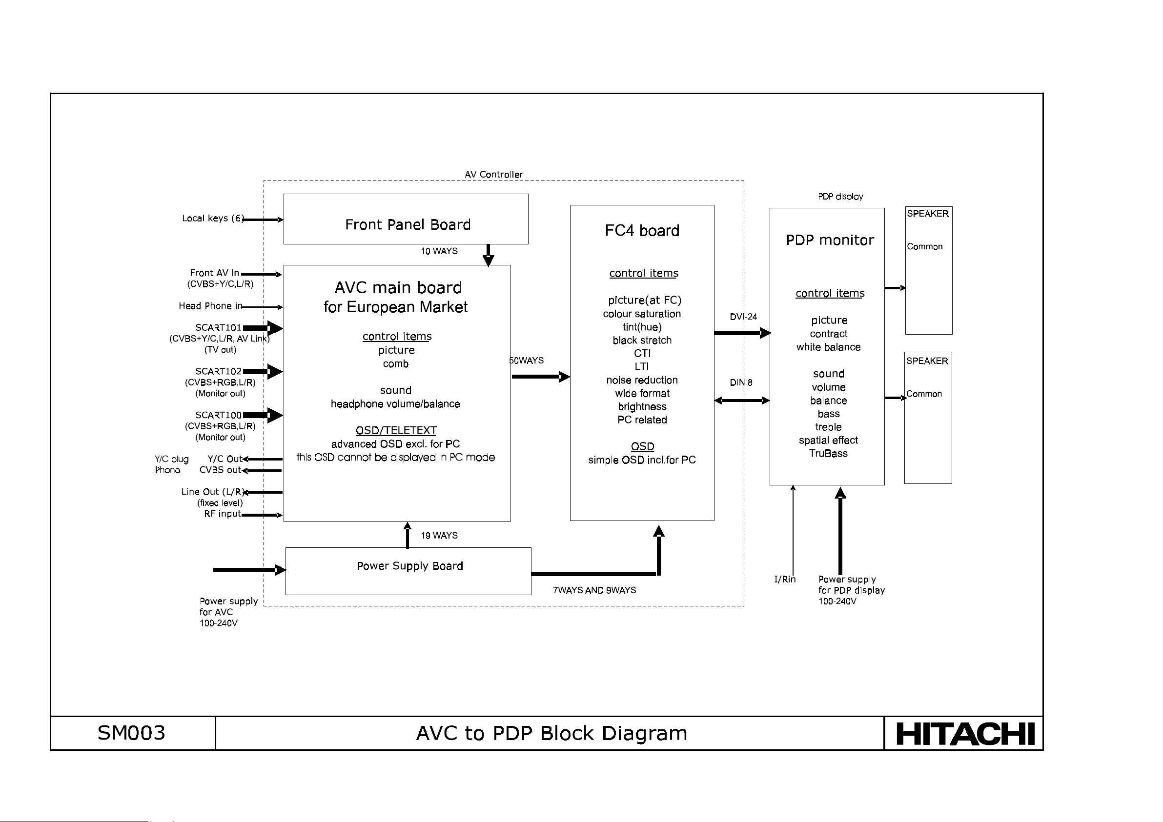
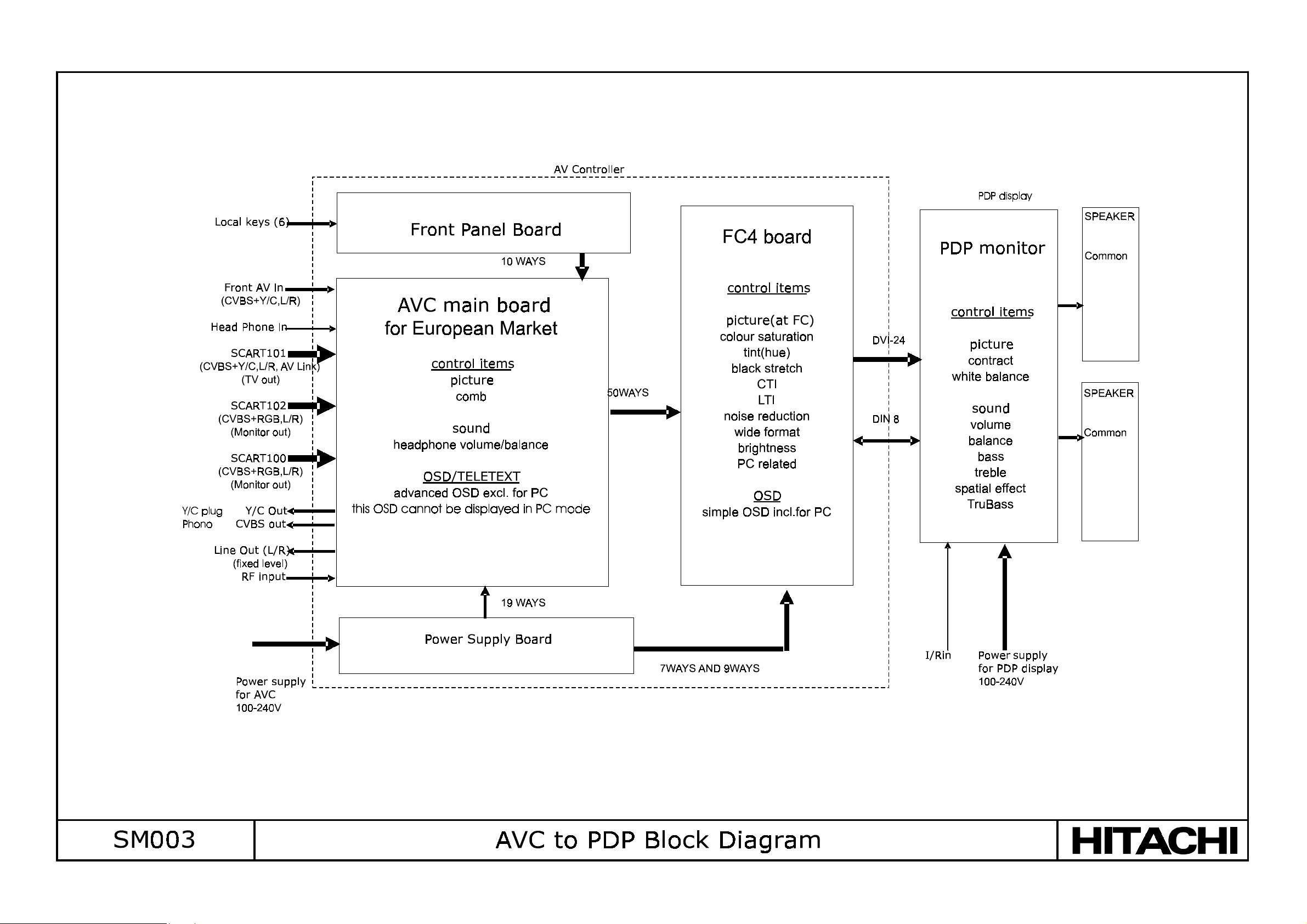
Block Diagrams
AVC to PDP Block Diagram
16
AVC Block Diagram
32PD3000 / 42PD3000
17
32PD3000 / 42PD3000
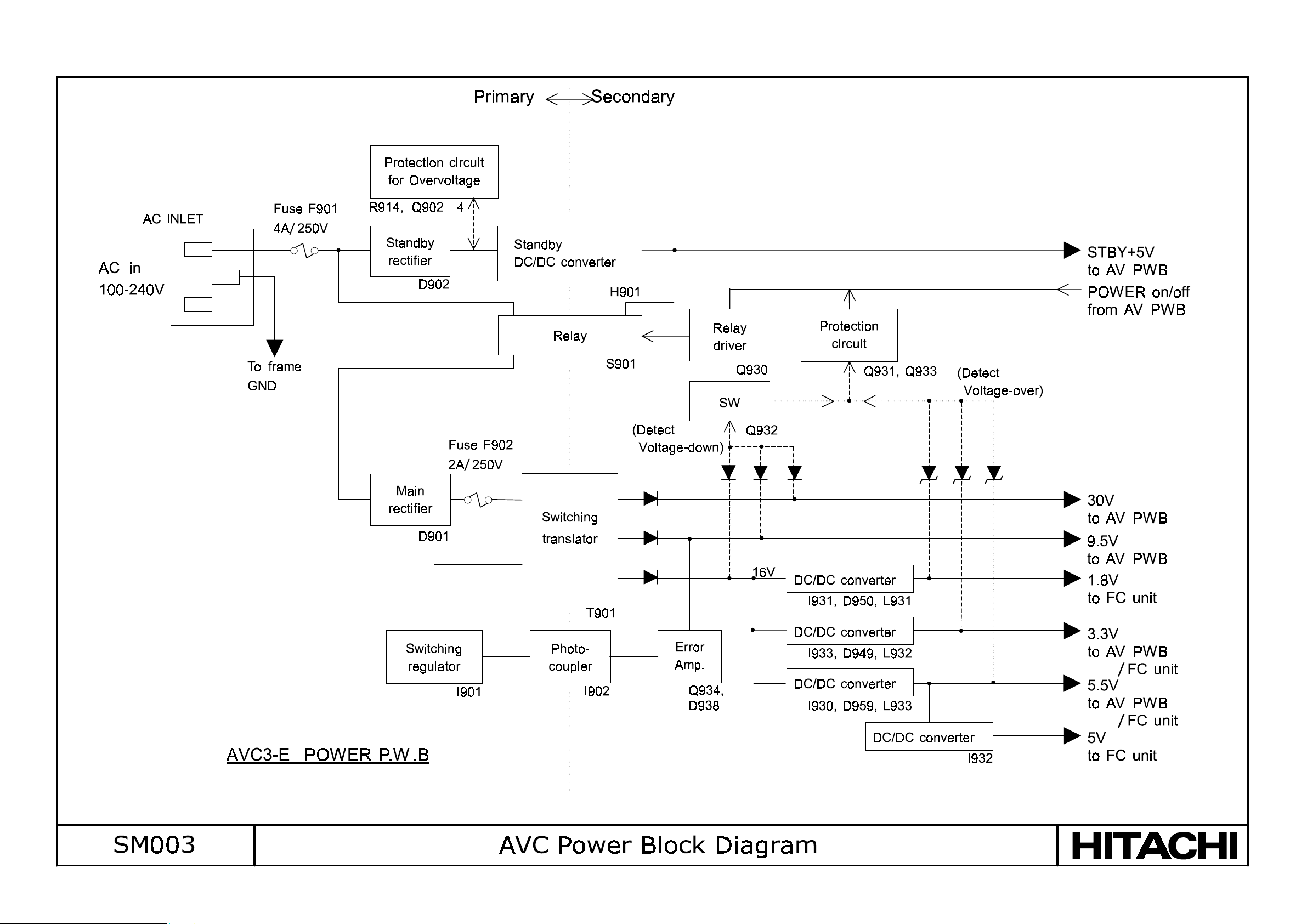
AVC Power Block Diagram
18
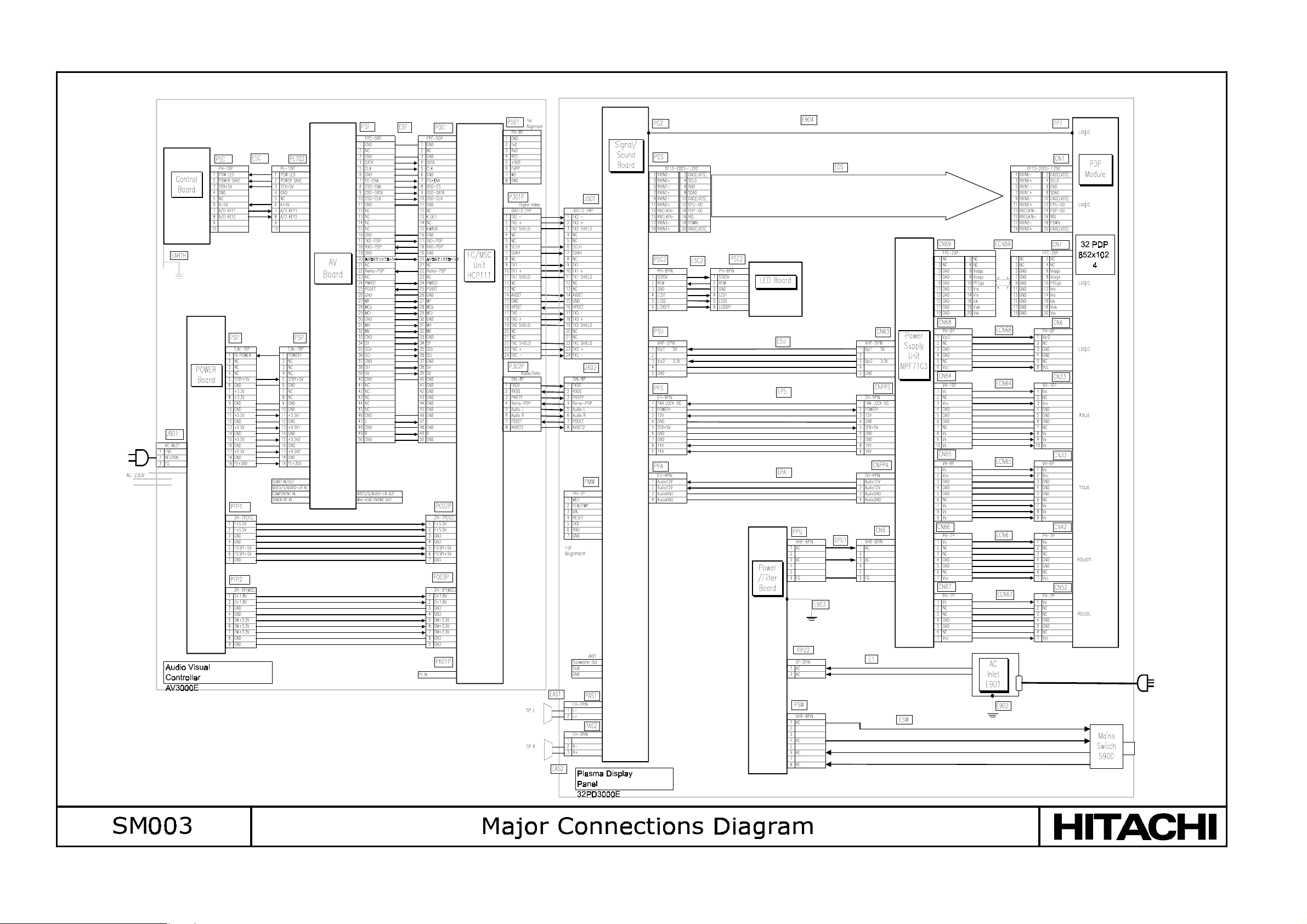
Major Connectors
32PD3000 / 42PD3000
19
32PD3000 / 42PD3000
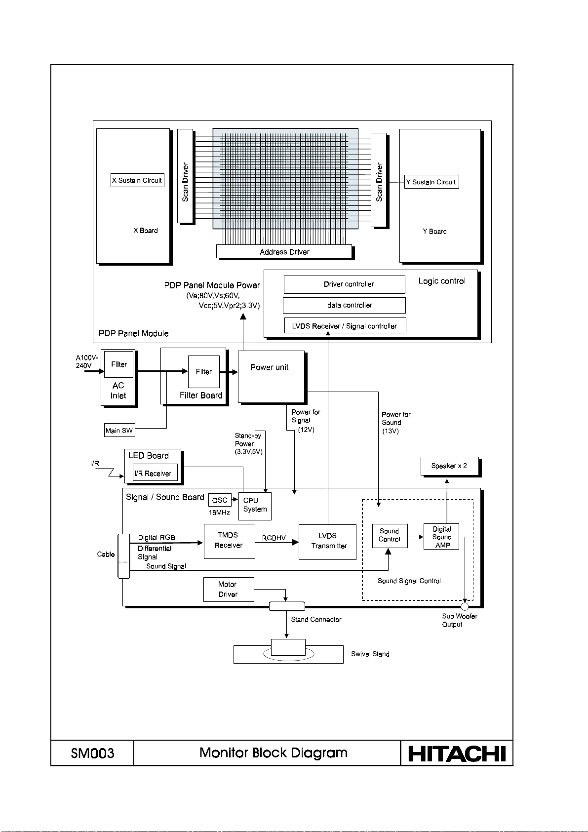
Monitor Block Diagram
20

32PD3000 / 42PD3000
Schematic Drawing Descriptions
Schematic Page 1 ; Tuner / Video Chroma
TUN100 Asymmetrical type tuner ; UV1316/A 1G-3 313914716781
SAW100 K3953M
SAW101 K9456M sound carrier 40.40MHz for standard L
IC100 Video chroma and video switch TDA9321H
TR100 TPWA01B - nominal centre freq. Fn1=6.0MHz and fn2=6.5MHz
TR101 TPWA04B - nominal centre freq. Fn1=5.5MHz and fn2=5.742MHz
X100 3.58MHz X'tal
X101 4.43MHz X'tal
Demodulated video signal is output from pin 10 going to sound traps
The TV signal from pin13 is also connected to SCART1 as TV signal output.
supply voltage ; +5V at pin 7 and +33V at pin 9
control by I2C, SDA at pin 5 and SCL at pin 4
picture carrier 33.90MHz, picture to sound carrier distance 6.5MHz for
standard L
VHF/UHF asymmetrical type tuner converts RF input signal to IF signal output
through pin 11.
AGC voltage is supplied at pin1 from IC100 pin62
IF output is going through buffer Q101 to SAW filter SAW100 for VIF at pin 2 and 3
of IC100 and to SAW101 for SIF at pin 63 and 64.
supply voltage ; +8V at pin 11 and 48 (AS)
control by I2C, SDA at pin 47 and SCL at pin 46
* IF demodulator and video chroma
There are two sound traps, TR100 for I/L signal and TR101 for BG, output from
which are switched by SOUND-SWITCH from IC301 pin 5
After group delay correction at pin 13, it is connected to pin 14 where TV picture is
supplied into video switch.
Quasi Split Sound converted from SIF input is output at pin 5 to connect with sound
decoder IC301
H and V sync pulses are output at pin 60 and 61 to go to FC/MSC for synchronization to
convert progressive scan. H pulse must be inverted by Q126.
When selecting one of video signal in video switch of IC100, CVBS signal is going to
COMB filter if the video is CVBS PAL/NTSC format.
Then Y/C separated signal is coming back at pin 28 and 29. The clock must be
provided from pin 30.
The video or Y/C signal selected pass through video chroma section and finally
converted to YUV format at pin 49, 50, 51
IC100 is supplied 4.43MHz and 3.58MHz clock from crystal X100 and X101,
which is automatically selected according to the signal received.
2 RGB inputs are also switched at the last stage in IC100. RGB signals are also
converted to YUV.
* video switch
21

32PD3000 / 42PD3000
input pin 14 TV signal input
pin 16 CVBS - SCART102 (AV2) input
pin 18 CVBS - SCART100 (AV3) input
pin 20 CVBS/Y - SCART101 (AV1) input
pin 21 C - SCART101 (AV1) input
pin 23 CVBS/Y - front AV (FRONT) input
pin 24 C - front AV (FRONT) input
pin 28 Y - from COMB filter
pin 29 C - from COMB filter
input pin 15 SCART102 (AV2) pin8 detection
control pin 17 SCART100 (AV3) pin8 detection
--- SCART101 (AV1) pin8 detection is done by micro IC704 pin28
output pin 26 go to COMB filter and phono video output
pin 32 go to micro for TELETEXT decoding
pin 34 go to SCART102(AV2) and SCART100(AV3) as monitor video output
output pin 20 L/L' switch for SAW filter in/out at SAW101
control pin 22 micro switch to switch SVHS or CVBS for front AV input
22

Schematic Page 2 ; Sound / AV3 Control
IC301 NICAM/A2 sound decoder and audio switch ; MSP3410
X300 18.432MHz
input pin 52 SCART101(AV1) sound L input
pin 53 SCART101(AV1) sound R input
pin 49 SCART102(AV2) sound L input
pin 50 SCART102(AV2) sound R input
pin 46 SCART100(AV3) sound L input
pin 47 SCART100(AV3) sound R input
pin 43 front AV (FRONT) sound L inout
pin 44 front AV (FRONT) sound R inout
pin 55 mono sound input from IC100
output pin 37 SCART101(AV1) sound L output
pin 36 SCART101(AV1) sound R output
pin 34 SCART102(AV2) / SCART3(AV3) sound L output
pin 33 SCART102(AV2) / SCART3(AV3) sound R output
pin 29 Speaker / Headphone/phone sound L output
pin 28 Speaker / Headphone/phone sound R output
output pin 5 SOUND SWITCH for trap of TV input signal
supply voltage ; +5V at pin 18 and pin 51
control by ; I2C, SDA at pin 10 and SCL at pin 9
* NICAM/A2 decoder and sound control
QSS signal is coming from IC100 to pin 58 through amplifier Q308/307. The signal
level at pin 58 should be 0.1 ~ 0.8Vpp.
Sound output L/R at pin 28 and 29 are connected through amplifier Q310/Q312 for L
and Q309/Q311 for R to adjust 500mVrms at PL700 pin 4 and 6 In the condition of AV
sound input 500mVrms, FM modulation 54%
Sound output L/R at pin 28 and 29 are also connected through IC300 TDA7433 and
IC303 to headphone.
* Audio switch
32PD3000 / 42PD3000
IC300 Basic audio processor ; TDA7433
supply voltage ; +8V at pin 17
control by ; I2C, SDA at pin 19 and SCL at pin 18
Monitor sound L/R outputs for speaker are connected headphone and phone out. IC300
contributes separate volume control
input pin 6 Audio sound L input
pin 5 Audio sound R input
23

32PD3000 / 42PD3000
output pin 16 Phono sound L output
pin 15 Phono sound R output
pin 14 Headphone sound L output
pin 13 Headphone sound R output
IC303 Headphone sound amplifier ; TDA2822D
Headphone sound L/R controlled its level by IC300 are amplified.
**** front AV video switch
PL300 connector for front control PCB
At pin 12 of PL700, CVBS from AV3 is coming.
At pin 11 of PL700, Y from AV3SVHS is coming
At pin 15 of PL700, C from AV3SVHS is coming to connect to pin 24 of IC100
supply voltage ; +6.5V at pin 2
At pin 9 indication of SVHS connector insertion is supplied to micro IC704 pin38 and
then it controls micro-switch from pin22 of IC100 in order to select Y from pin11 of
PL700 (micro-sw=H) or to select CVBS from pin12 of PL700 (micro-sw=L)
IC302
(OPTION)
TDA8440 is the option in the future. This is not used for this model.
24

32PD3000 / 42PD3000
Schematic Page 3 ; Interface Board (component input, progressive sync
separation, centre audio channel
IC08 Sync separation for Component (progressive) input ; TA1370
XC01 50KHz
supply voltage ; +9V at pin 11
control by ; I2C, SDA at pin 21 and SCL at pin 22
Sync separation for progressive YPbPr input (50Hz and 60Hz) are carried out at
TA1370.
Input video signal is specifically given from AV4 and connected at pin 26 through
clamping circuit constituted with QC25~QC28
Sync separation for all input signal other than Progressive input are carried out at
TDA9321 (page1)
TA1370 includes switch of sync signal (H and V) between H/V input (pin I and
pin2) from TDA9321 and internal sync separation.
TA1370 outputs H at pin16 and V at pin 28, which are connected to PSF for FC4
board. There are 2 inputs of the connector for each main and sub.
H output at pin 16 on TA1370 is fed to IC10 to shorten H pulse waveform to avoid
jittering.
)
IC02/IC03 YUV/RGB switch ; TA1287
input IC02 YUV; Main signal
IC03 YUV; from IC02
YUV ; at pin 1/2/3, Y:1Vpp (incl.sync), UV:0.3Vpp
RGB ; at pin 6/7/8, 0.7Vpp
output IC02 connect to IC03
IC03 connect to FC4 through buffers
YUV ; at pin13/14/15, Y:1Vpp (incl.sync), UV:0.3Vpp
IC02 0V; through
IC03 always 1.6V:RGB --> YUV
control IC02 0V; external (Components input)
IC03 0V; Video
supply voltage ; +9V at pin 16
control by ; DC voltage at pin 9/10/11 and matrix at pin 16
matrix control of RGB input (YUV can also input. In this case, matrix control
should be through)
IC04/IC05/IC06 Analogue switch ; BU4066
supply voltage +9V at pin 14
25

32PD3000 / 42PD3000
IC04
IC05
IC06
Audio switch, main L/R or AV4 (components input) L/R. main L/R comes
from MSP3410 audio switch.
Video switch, Front video or AV4 (in case of YCbCr normal components),
which is connected to TDA9321 for sync separation
Audio switch, Centre sound or AV4 (components input) L/R. Output goes
to IC04 to switch another audio input.
IC07 Analogue Switch for Sub video ; BU4053
supply voltage ; +9V at pin 16
2 inputs, main YUV from IC03 and RGB from micro (TELETXT), are switched
and connected to sub video input for FC4
This is enabled when TV+TEXT is selected (SUB TELETEXT), and when PC
window is selected (SUB VIDEO)
IC09 I/O expanders ; M62320FP
supply voltage ; +5V at pin 13
control by ; I2C, SDA at pin 3 and SCL at pin 2
D00 pin 4
D01 pin 5
D02 pin 6
D03 pin 7
D04 pin 9
D05 pin 10
D06 pin 11
D07 pin 12
component video IC02, IC05 components input other than components
Matrix IC02 RGB --> YUV through
PC IC07 Not PC mode (SUB TEXT) PC mode (SUB video in PCW)
OSD-blank IC03 kill OSD OSD enabled
Cinema IC06, IC04 Audio centre not selected Audio centre selected
Clamp-source IC05 CP from TA1370 SC from TDA9321
TV/TEXT IC03 TEXT (select RGB input) TV
N.C.
connect to L
H
26

32PD3000 / 42PD3000
Schematic Page 4 ; Power Circuit (Voltage Regulator) / Level Shifter
Power supply connector PSP from Power Supply board
1 POWER1 Power ON/Stand-by control H;ON, L;Stand-by
2 N.C.
3 N.C.
4 N.C.
5 +5VSTB Stand-by 5V for micro controller circuit
6 GND
7 N.C.
8 N.C.
9 GND
10 GND
11 +5.5V1 5.5V supply 1
12 GND
13 +9.5V1 9.5V supply 1
14 GND
15 +5.5V2 5.5V supply 2
16 GND
17 +9.5V2 9.5V supply2
18 GND
19 FE+30V 30V supply for tuner
Voltage regulators
I603
BA06T Input +9.5V2 - Output +8V
For video chroma circuit (page1)
IC602
SI-3050LSA Input +5.5V1 - Output +5VFE
For tuner (page1)
IC603
SI-3050LSA Input +5.5V2 - Output +5V
For audio processor circuit (page2), comb filter (page6)
IC601
SI-3033LSA Input +5VSTB - Output 3.3VSTB
For micro controller circuit
Q602
TK11125M Input +5VSTB - Output 2.5VSTB
For micro controller circuit
IC604
BA09FP Input +9.5V1 - Output +9V
For interface circuit (page 3)
Level shift for control buses
Q607
Q603
Q604
Q605
Q614
BSS138 3WB-DATA to change from 3V3 to 5V
2SC2412K 3WB-CLOCK to invert with 5V range
2SC2412K FC-ENABLE to invert with 5V range
2SC2412K MSC-ENABLE to invert with 5V range
BSS138 1900TX to change from 3V3 to 5V
27
 Loading...