

HIT HSC119 Datasheet
HSC119
Silicon Epitaxial Planar Diode for High Speed Switching
Features
• Low capacitance. (C=2.0pF max)
• Short reverse recovery time. (trr =3.0ns max)
• U ltra small F lat P ackage (UFP) is suitable for surface mount design.
Ordering Information
Type No. Laser Mark Package Code
HSC119 H1 UFP
ADE-208-615 (Z)
Rev 0
Apr. 1998
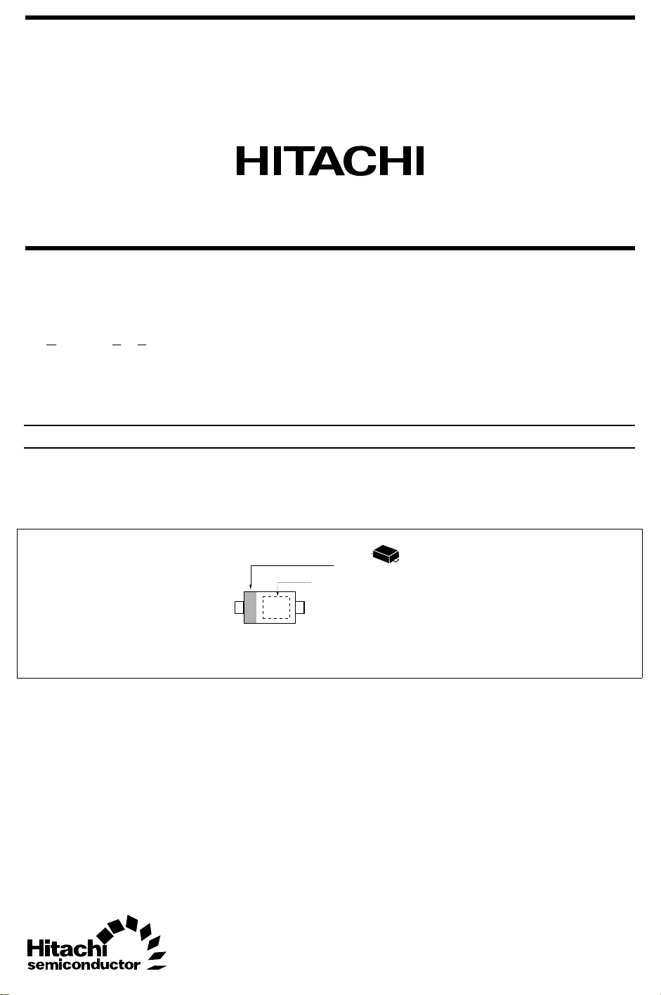
Outline
Cathode mark
Mark
12
H1
1. Cathode
2. Anode
HSC119
Absolute Maximum Ratings (Ta = 25°C)
Item Symbol Value Unit
Peak reverse voltage V
Reverse voltage V
Average forward current I
Peak rectified current I
Non-Repetitive peak
RM
R
O
FM
*1
I
FSM
forward surge current
Junction temperature Tj 125 °C
Storage temperature Tstg –55 to +125 °C
Note 1. Within 1µs forward surge current.
Electrical Characteristics (Ta = 25°C)
Item Symbol Min Typ Max Unit Test Condition
Forward voltage V
Reverse current I
F1
V
F2
R
Capacitance C — — 2.0 pF VR = 0V, f = 1 MHz
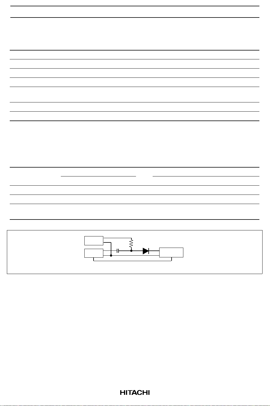
Reverse recovery
*1
time
t
rr
Notes 1. Reverse recovery time test circuit
— — 0.8 V IF = 10 mA
— — 1.2 IF = 100 mA
— — 0.1 µAVR = 80V
— — 3.0 ns IF = 10 mA, VR = 6V RL=50Ω
85 V
80 V
100 mA
300 mA
4A
DC
Ro =50
Ω
Pulse
Generator
Supply
0.1µF
Trigger
Ω
3k
Sampling
Oscilloscope
Rin =50
Ω
2
 Loading...