

HIT HN58S65AT-15 Datasheet

HN58S65A Series
64 k EEPROM (8-kword × 8-bit)
Ready/Busy function
ADE-203-691A (Z)
Preliminary
Rev. 0.3
Nov. 1997
Description
The Hitachi HN58S65A series is electrically erasable and programmable ROM organized as 8192-word
× 8-bit. It has realized high speed, low power consumption and high reliability by employing advanced
MNOS memory technology and CMOS process and circuitry technology. They also have a 64-byte
page programming function to make their write operations faster.
Features
• Single supply: 2.2 to 3.6 V
• Access time: 150 ns (max)
• Power dissipation
Active: 10 mW/MHz (typ)
Standby: 36 µW (max)
• On-chip latches: address, data, CE, OE, WE
• Automatic byte write: 15 ms (max)
• Automatic page write (64 bytes): 15 ms (max)
• Ready/Busy
• Data polling and Toggle bit
• Data protection circuit on power on/off
• Conforms to JEDEC byte-wide standard
• Reliable CMOS with MNOS cell technology
• 105 erase/write cycles (in page mode)
• 10 years data retention
• Software data protection
• Industrial versions (Temperature range: – 40 to + 85˚C) are also available.
Preliminary: This document contains information on a new product. Specifications and information
contained herein are subject to change without notice.
HN58S65A Series
Ordering Information
Type No. Access time Package
HN58S65AT-15 150 ns 28-pin plastic TSOP(TFP-28DB)
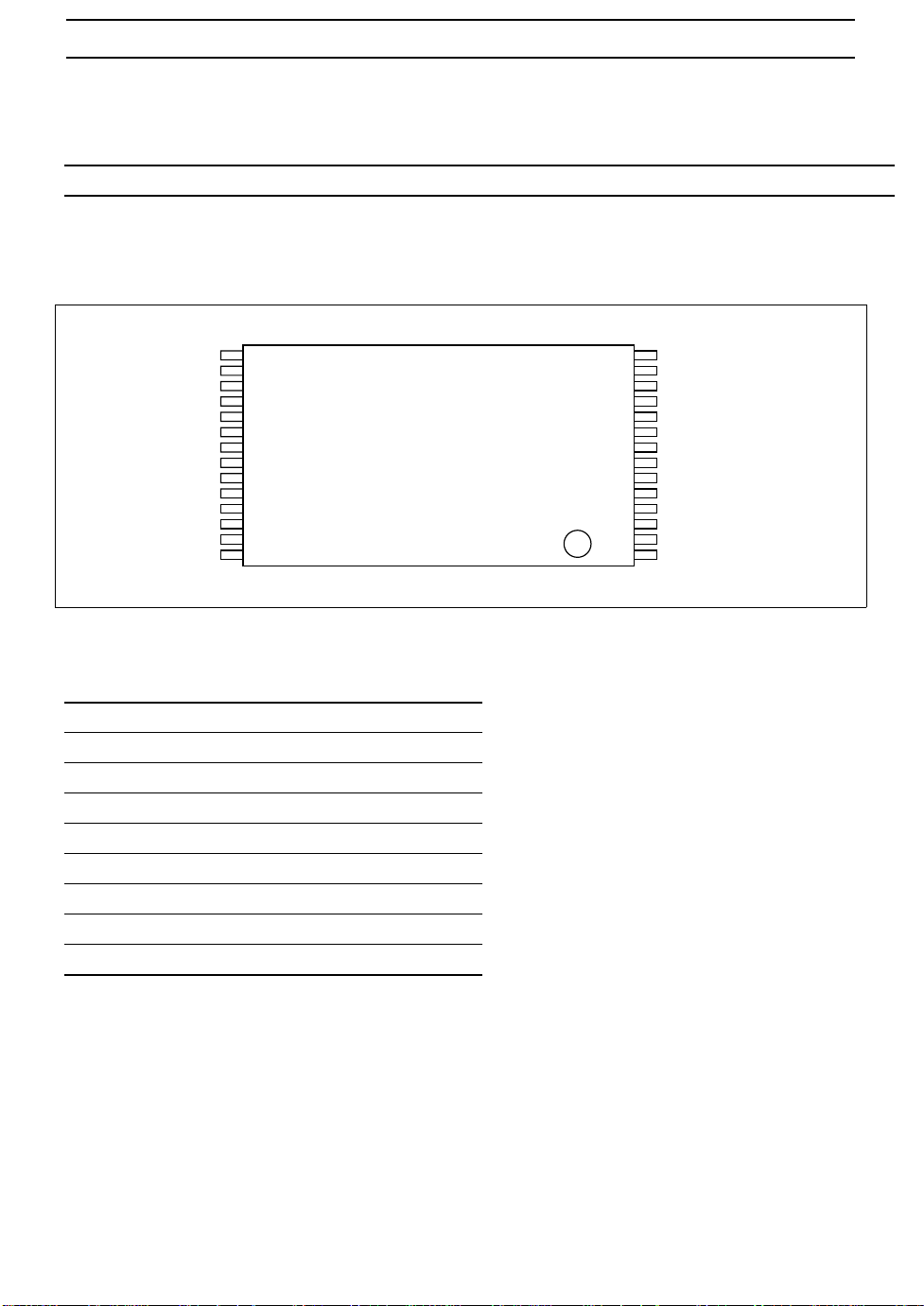
Pin Arrangement
HN58S65AT Series
SS
15
16
17
18
19
20
21
22
23
24
25
26
27
28
(Top view)
A2
A1
A0
I/O0
I/O1
I/O2
V
I/O3
I/O4
I/O5
I/O6
I/O7
CE
A10
14
13
12
11
10
9
8
7
6
5
4
3
2
1
A3
A4
A5
A6
A7
A12
RDY/Busy
V
CC
WE
NC
A8
A9
A11
OE
Pin Description
Pin name Function
A0 to A12 Address input
I/O0 to I/O7 Data input/output
OE Output enable
CE Chip enable
WE Write enable
V
CC
V
SS
RDY/Busy Ready busy
NC No connection
Power supply
Ground
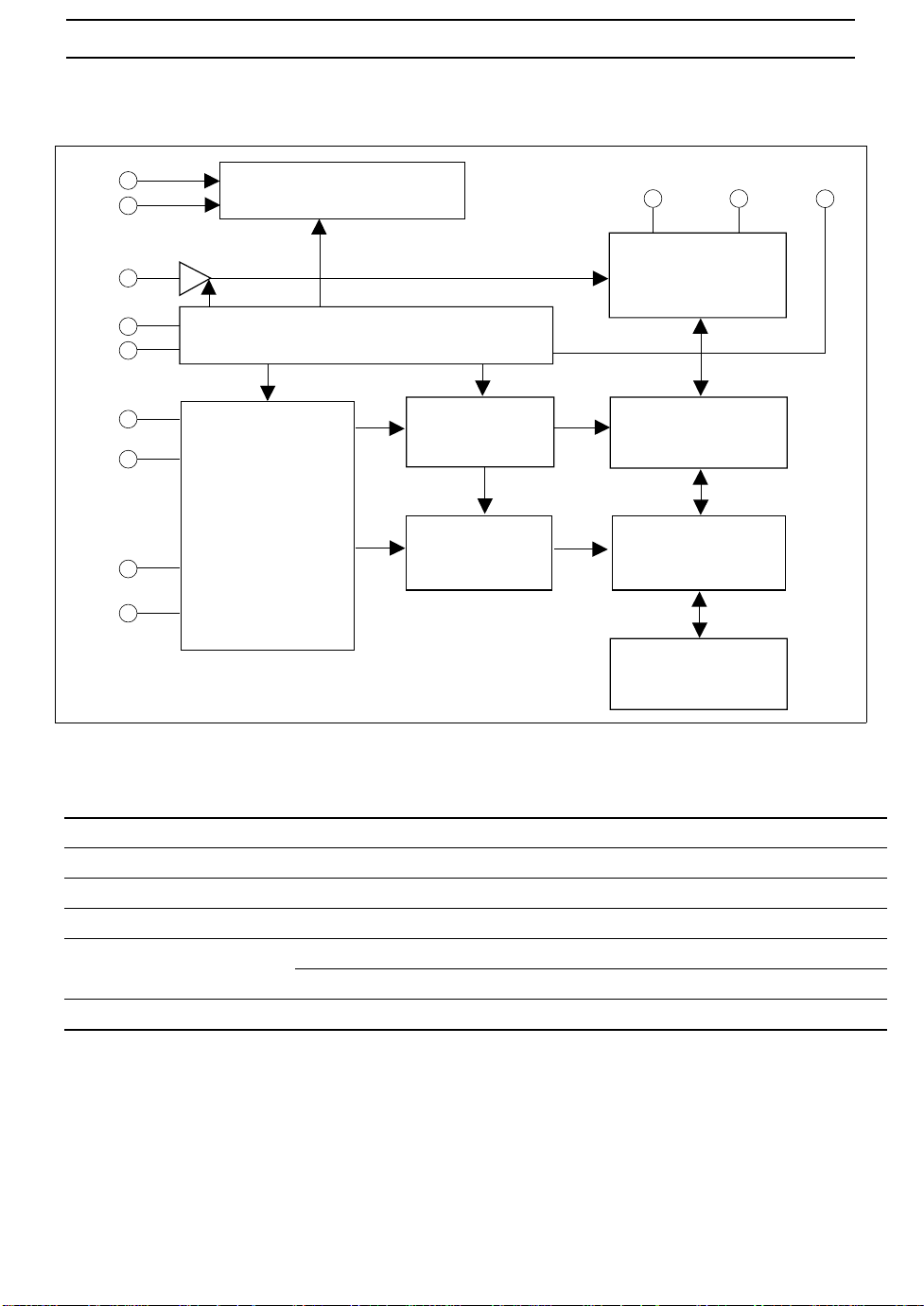
Block Diagram
V
CC
V
SS
OE
CE
WE
High voltage generator
Control logic and timing
HN58S65A Series
to
I/O0 I/O7
I/O buffer
and
input latch
RDY/Busy
A0
to
Y decoder
Y gating
A5
Address
buffer and
latch
X decoder
Memory array
A6
to
A12
Data latch
Operation Table
Operation CE OE WE RDY/Busy I/O
Read V
Standby V
Write V
Deselect V
IL
IH
IL
IL
V
×*
V
V
IL
1
IH
IH
Write Inhibit ××V
Data Polling V
× V
IL
IL
V
IL
Notes: 1. × : Don’t care
V
IH
High-Z Dout
× High-Z High-Z
V
IL
V
IH
IH
High-Z to V
Din
OL
High-Z High-Z
——
× ——
V
IH
V
OL
Dout (I/O7)

HN58S65A Series
Absolute Maximum Ratings
Parameter Symbol Value Unit
Power supply voltage relative to V
Input voltage relative to V
Operating temperature range *
SS
2
SS
V
CC
Vin –0.5*1 to +7.0*
Topr 0 to +70 ˚C
Storage temperature range Tstg –55 to +125 ˚C
Notes: 1. Vin min : –3.0 V for pulse width ≤ 50 ns.
2. Including electrical characteristics and data retention.
3. Should not exceed V
+ 1.0 V.
CC
Recommended DC Operating Conditions
Parameter Symbol Min Typ Max Unit
Supply voltage V
Input voltage V
CC
V
SS
IL
V
IH
Operating temperature Topr 0 — 70 ˚C
Notes: 1. VIL min: –1.0 V for pulse width ≤ 50 ns.
2. V
max: VCC + 1.0 V for pulse width ≤ 50 ns.
IH
2.2 3.0 3.6 V
000V
–0.3*
VCC × 0.7 — VCC + 0.3*2V
–0.6 to +7.0 V
3
1
— 0.4 V
V
DC Characteristics (Ta = 0 to + 70˚C, VCC = 2.2 to 3.6 V)
Parameter Symbol Min Typ Max Unit Test conditions
Input leakage current I
Output leakage current I
Standby VCC current I
Operating VCC current I
Output low voltage V
Output high voltage V
LI
LO
CC1
I
CC2
CC3
OL
OH
——2µAVCC = 5.5 V, Vin = 5.5 V
——2µAVCC = 5.5 V, Vout = 5.5/0.4 V
— 1 to 2 3.5 µA CE = V
— — 500 µA CE = V
CC
IH
— — 6 mA Iout = 0 mA, Duty = 100%,
Cycle = 1 µs at V
— — 12 mA Iout = 0 mA, Duty = 100%,
Cycle = 150 ns at V
— — 0.4 V IOL = 1.0 mA
VCC × 0.8 — — V IOH = –100 µA
= 3.6 V
CC
CC
= 3.6 V

HN58S65A Series
Capacitance (Ta = 25˚C, f = 1 MHz)
Parameter Symbol Min Typ Max Unit Test conditions
Input capacitance Cin*
Output capacitance Cout*
1
1
Note: 1. This parameter is sampled and not 100% tested.
AC Characteristics (Ta = 0 to + 70˚C, VCC = 2.2 to 3.6 V)
Test Conditions
• Input pulse levels : 0.4 V to 2.4 V (VCC = 2.7 to 3.6 V), 0.4 V to 1.9 V (VCC = 2.2 to 2.7 V)
• Input rise and fall time : ≤ 5 ns
• Input timing reference levels : 0.8, 1.8 V
• Output load : 1TTL Gate +100 pF
• Output reference levels : 1.5 V, 1.5 V (VCC = 2.7 to 3.6 V)
1.1 V, 1.1 V (VCC = 2.2 to 2.7 V)
— — 6 pF Vin = 0 V
— — 12 pF Vout = 0 V
Read Cycle
HN58S65A
-15
Parameter Symbol Min Max Unit Test conditions
Address to output delay t
CE to output delay t
OE to output delay t
Address to output hold t
OE (CE) high to output float*1t
ACC
CE
OE
OH
DF
— 150 ns CE = OE = VIL, WE = V
— 150 ns OE = VIL, WE = V
10 80 ns CE = VIL, WE = V
0—nsCE = OE = VIL, WE = V
080nsCE = VIL, WE = V
IH
IH
IH
IH
IH
HN58S65A Series
Write Cycle
Test
conditions
ms
Parameter Symbol Min*
Address setup time t
Address hold time t
CE to write setup time (WE controlled) t
CE hold time (WE controlled) t
WE to write setup time (CE controlled) t
WE hold time (CE controlled) t
OE to write setup time t
OE hold time t
Data setup time t
Data hold time t
WE pulse width (WE controlled) t
CE pulse width (CE controlled) t
Data latch time t
Byte load cycle t
Byte load window t
Write cycle time t
Time to device busy t
Write start time t
AS
AH
CS
CH
WS
WH
OES
OEH
DS
DH
WP
CW
DL
BLC
BL
WC
DB
DW
0——ns
150 — — ns
0——ns
0——ns
0——ns
0——ns
0——ns
0——ns
150 — — ns
0——ns
200 — — ns
200 — — ns
200 — — ns
0.4 — 30 µs
100 — — µs
— — 15*
120 — — ns
4
0*
2
Typ Max Unit
3
——ns
Notes: 1. tDF is defined as the time at which the outputs achieve the open circuit conditions and are no
longer driven.
2. Use this device in longer cycle than this value.
3. t
must be longer than this value unless polling techniques or RDY/Busy are used. This
WC
device automatically completes the internal write operation within this value.
4. Next read or write operation can be initiated after t
if polling techniques or RDY/Busy are
DW
used.
5. A6 through A12 are page addresses and these addresses are latched at the first falling edge
of WE.
6. A6 through A12 are page addresses and these addresses are latched at the first falling edge
of CE.
7. See AC read characteristics.
 Loading...