HN58C65 Series
8192-word × 8-bit Electrically Erasable and Programmable CMOS
ROM
ADE-203-374A (Z)
Rev. 1.0
Apr. 12, 1995
Description
The Hitachi HN58C65 is a electrically erasable and programmable ROM organized as 8192-word × 8-bit. It
realizes high speed, low power consumption, and a high level of reliability, employing advanced MNOS
memory technology and CMOS process and circuitry technology. It also has a 32-byte page programming
function to make its erase and write operations faster.
Features
• Single 5 V Supply
• On chip latches: address, data, CE, OE, WE
• Automatic byte write: 10 ms max
• Automatic page write (32 byte): 10 ms max
• Fast access time: 250 ns max
• Low power dissipation: 20 mW/MHz typ (Active)
2.0 mW typ (Standby)
• Data polling and Ready/Busy
• Data protection circuity on power on/power off
• Conforms to JEDEC byte-wide standard
• Reliable CMOS with MNOS cell technology
• 105 erase/write cycles (in page mode)
• 10 year data retention
Ordering Information
Type No. Access Time Package
HN58C65P-25 250 ns 600 mil 28 pin plastic DIP (DP-28)
HN58C65FP-25 250 ns 28 pin plastic SOP*1 (FP-28D/DA)
Note: 1. T is added to the end of the type no. for a SOP of 3.0 mm (max) thickness.

HN58C65 Series
Pin Arrangement
HN58C65P/FP Series
RDY/Busy
V
A12
A7
A6
A5
A4
A3
A2
A1
A0
I/O0
I/O1
I/O2
SS
1
2
3
4
5
6
7
8
9
10
11
12
13
14
28
27
26
25
24
23
22
21
20
19
18
17
16
15
(Top View)
Pin Description
Pin Name Function
A0 – A12 Address input
I/O1 – I/O7 Data input/output
OE Output enable
CE Chip enable
WE Write enable
V
CC
V
SS
NC No connection
RDY/Busy Ready/Busy
Power (+5 V)
Ground
V
CC
WE
NC
A8
A9
A11
OE
A10
CE
I/O7
I/O6
I/O5
I/O4
I/O3
2

Block Diagram
HN58C65 Series
V
CC
V
SS
OE
CE
WE
A0
A4
A5
A12
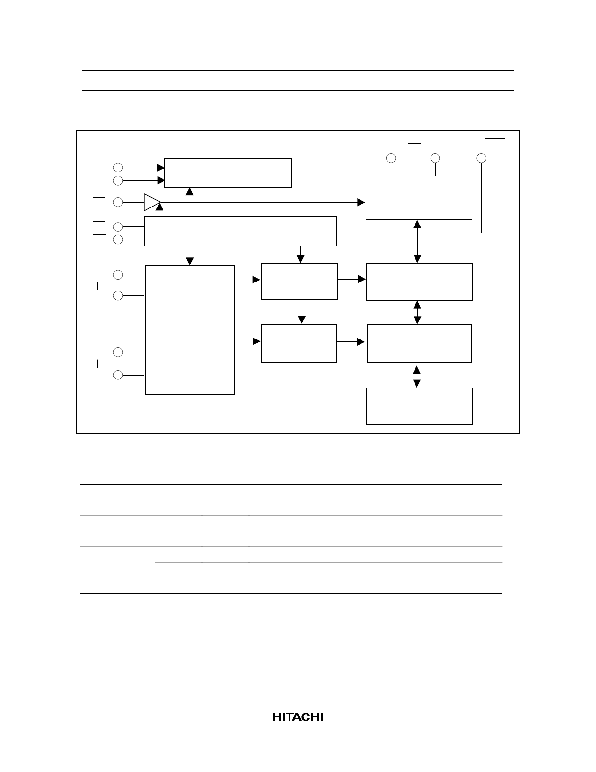
High Voltage Generator
Control Logic and Timing
Address
Buffer and
Latch
Y Decoder
X Decoder
I/O0 I/O7
I/O Buffer
and
Input Latch
Y Gating
Memory Array
Data Latch
RDY/Busy
Mode Selection
Pin Mode CE OE WE RDY/Busy I/O
Read V
Standby V
Write V
Deselect V
IL
IH
IL
IL
Write inhibit X X V
XVILX High-Z —
Data polling V
IL
Note: 1. X = Don’t care
V
IL
*1
X
V
IH
V
IH
V
IL
V
IH
High-Z Dout
X High-Z High-Z
V
IL
V
IH
IH
V
IH
High-Z to V
OL
Din
High-Z High-Z
V
OL
Data out (I/O7)
3

HN58C65 Series
Absolute Maximum Ratings
Parameter Symbol Value Unit
Supply voltage
Input voltage
*1
*1
Operating temperature range
Storage temperature range Tstg –55 to +125 °C
Notes: 1. With respect to V
2. –3.0 V for pulse width ≤ 50 ns.
3. Including electrical characteristics and data retention.
Recommended DC Operating Conditions
Parameter Symbol Min Typ Max Unit
Supply voltage V
Input voltage V
Operating temperature Topr 0 — 70 °C
V
CC
–0.6 to +7.0 V
Vin –0.5*2 to +7.0 V
*3
Topr 0 to +70 °C
SS
CC
IL
V
IH
4.5 5.0 5.5 V
–0.3 — 0.8 V
2.2 — VCC + 1 V
4

HN58C65 Series
DC Characteristics (Ta = 0 to +70°C, VCC = 5 V ± 10%)
Parameter Symbol Min Typ Max Unit Test Conditions
Input leakage current I
Output leakage current I
VCC current (Standby) I
VCC current (Active) I
Input low voltage V
Input high voltage V
Output low voltage V
Output high voltage V
LI
LO
CC1
CC2
IL
IH
OL
OH
Note: 1. –1.0 V for pulse width ≤ 50 ns
——2 µAV
——2 µAV
——1 mACE = VIH, CE = V
— — 8 mA Iout = 0 mA
— — 25 mA Iout = 0 mA
*1
–0.3
— 0.8 V
2.2 — VCC + 1 V
— — 0.4 V IOL = 2.1 mA
2.4 — — V I
= 5.5 V
CC
Vin = 5.5 V
= 5.5 V
CC
Vout = 5.5/0.4 V
Duty = 100%
Cycle = 1 µs at
V
= 5.5 V
CC
Duty = 100%
Cycle = 250 ns at
V
= 5.5 V
CC
= –400 µA
OH
CC
Capacitance (Ta = 25°C, f = 1 MHz)
Parameter Symbol Min Typ Max Unit Test Conditions
Input capacitance
Output capacitance
*1
*1
Cin — — 6 pF Vin = 0 V
Cout — — 12 pF Vout = 0 V
Note: 1. This parameter is periodically sampled and not 100% tested.
AC Characteristics (Ta = 0 to +70°C, VCC = 5 V ± 10%)
Test Conditions
• Input pulse levels: 0.4 V to 2.4 V
• Input rise and fall time: ≤ 20 ns
• Output load: 1TTL gate + 100 pF
• Reference levels for measuring timing: 0.8 V and 2 V
5
 Loading...