

HM62W16258B Series
4 M SRAM (256-kword × 16-bit)
ADE-203-976B (Z)
Rev. 2.0
Oct. 14, 1999
Description
The Hitachi HM62W16258B Series is 4-Mbit static RAM organized 262,144-word × 16-bit. HM62W16258B
Series has realized higher density, higher performance and low power consumption by employing Hi-CMOS
process technology. It offers low power standby power dissipation; therefore, it is suitable for battery backup
systems. It is packaged in standard 44-pin plastic TSOPII.
Features
• Single 3.3 V supply: 3.3 V ± 0.3 V
• Fast access time: 55 ns/70 ns (max)
• Power dissipation:
Active: 9.9 mW (typ)
Standby: 3.3 µW (typ)
• Completely static memory.
No clock or timing strobe required
• Equal access and cycle times
• Common data input and output.
Three state output
• Battery backup operation.
HM62W16258B Series
Ordering Information
Type No. Access time Package
HM62W16258BLTT-5
HM62W16258BLTT-7
HM62W16258BLTT-5SL
HM62W16258BLTT-7SL
55 ns
70 ns
55 ns
70 ns
400-mil 44-pin plastic TSOPII (normal-bend type) (TTP-44DB)
2
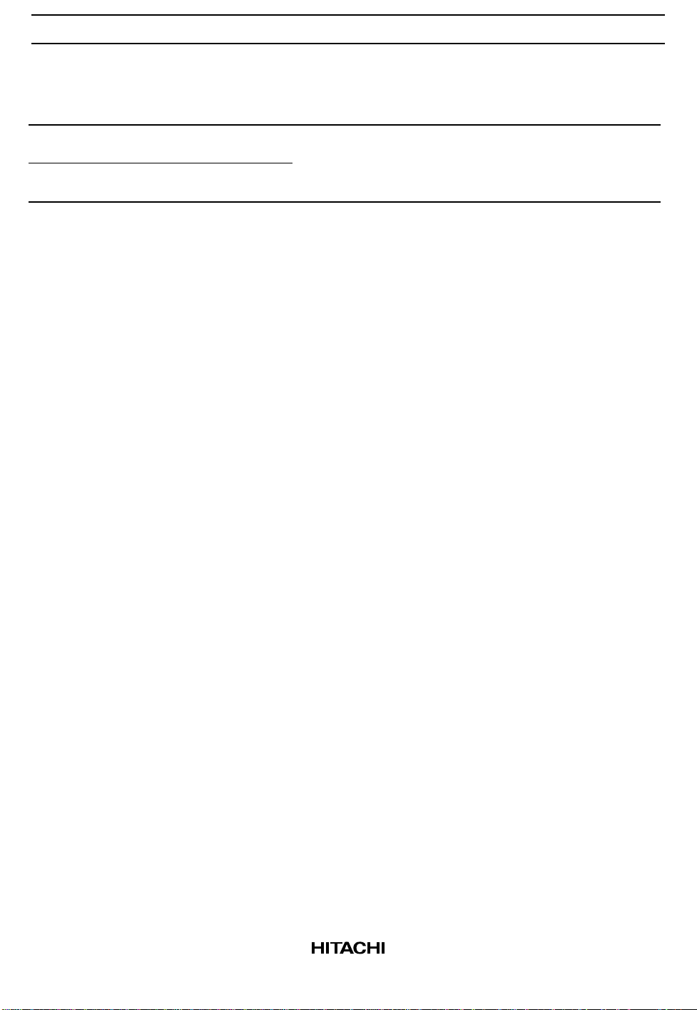
Pin Arrangement
HM62W16258B Series
44-pin TSOP
A4
A3
A2
A1
A0
CS
I/O0
I/O1
I/O2
I/O3
V
CC
V
SS
I/O4
I/O5
I/O6
I/O7
WE
A17
A16
A15
A14
A13
1
2
3
4
5
6
7
8
9
10
11
12
13
14
15
16
17
18
19
20
21
22
(Top view)
44
43
42
41
40
39
38
37
36
35
34
33
32
31
30
29
28
27
26
25
24
23
A5
A6
A7
OE
UB
LB
I/O15
I/O14
I/O13
I/O12
V
SS
V
CC
I/O11
I/O10
I/O9
I/O8
NC
A8
A9
A10
A11
A12
Pin Description
Pin name Function
A0 to A17 Address input
I/O0 to I/O15 Data input/output
CS Chip select
WE Write enable
OE Output enable
LB Lower byte select
UB Upper byte select
V
CC
V
SS
NC No connection
Power supply
Ground
3
HM62W16258B Series
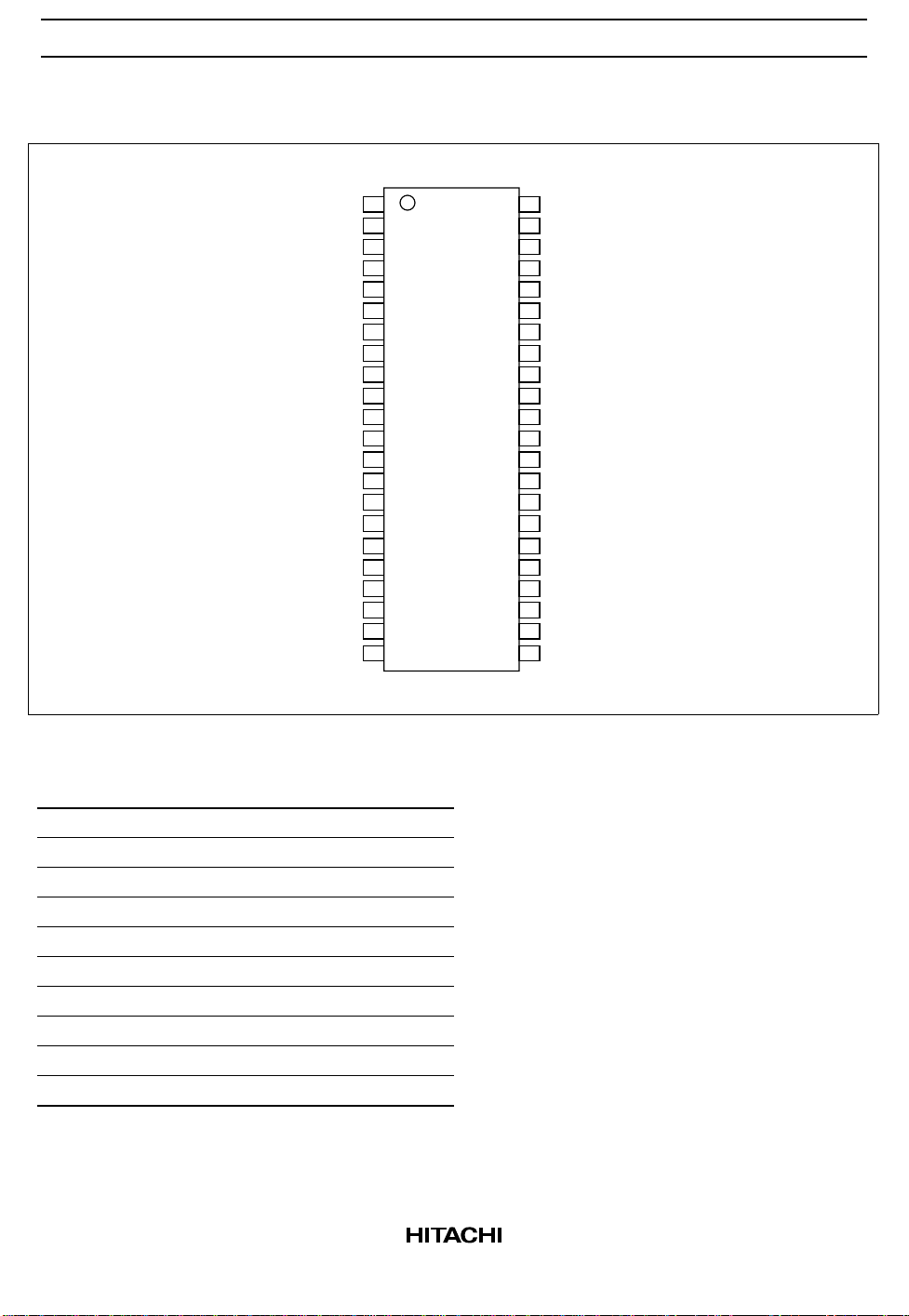
Block Diagram
LSB
MSB
A4
A3
A15
A14
A16
A1
A2
A17
A0
A13
I/O0
I/O15
Row
decoder
Input
data
control
V
CC
V
SS
•
•
•
•
•
•
•
Memory matrix
2,048 x 2,048
Column I/O
•
•
Column decoder
CS
LB
UB
WE
OE
Control logic
LSB
A7
A6
•
•
A5
A8
A9
A10
A11
A12
MSB
4
HM62W16258B Series
Operation Table
CS WE OE UB LB I/O0 to I/O7 I/O8 to I/O15 Operation
H ××××High-Z High-Z Standby
×××H H High-Z High-Z Standby
L H L L L Dout Dout Read
L H L H L Dout High-Z Lower byte read
L H L L H High-Z Dout Upper byte read
LL×L L Din Din write
LL×H L Din High-Z Lower byte write
LL×L H High-Z Din Upper byte write
LHH××High-Z High-Z Output disable
Note: H: VIH, L: VIL, ×: VIH or V
Absolute Maximum Ratings
Parameter Symbol Value Unit
Power supply voltage relative to V
Terminal voltage on any pin relative to V
Power dissipation P
Storage temperature range Tstg –55 to +125 °C
Storage temperature range under bias Tbias –10 to +85 °C
Notes: 1. VT min: –3.0 V for pulse half-width ≤ 30 ns.
2. Maximum voltage is +4.6 V.
IL
SS
SS
V
CC
V
T
T
–0.5 to + 4.6 V
–0.5*1 to VCC + 0.3*
2
V
1.0 W
DC Operating Conditions
Parameter Symbol Min Typ Max Unit Note
Supply voltage V
Input high voltage V
Input low voltage V
CC
V
SS
IH
IL
Ambient temperature range Ta 0 — 70 °C
Note: 1. VIL min: –3.0 V for pulse half-width ≤ 30 ns.
3.0 3.3 3.6 V
000V
2.0 — VCC + 0.3 V
–0.3 — 0.8 V 1
5

HM62W16258B Series
DC Characteristics
Parameter Symbol Min Typ*1Max Unit Test conditions
Input leakage current |I
Output leakage current |ILO|— —1 µACS = VIH or OE = VIH or WE = VIL, or
Operating current I
Average
HM62W16258B-5 I
operating
current
HM62W16258B-7 I
Standby current I
Standby current I
Output high voltage V
Output low voltage V
Notes: 1. Typical values are at VCC = 3.0 V, Ta = +25°C and not guaranteed.
2. This characteristic is guaranteed only for L-version.
3. This characteristic is guaranteed only for L-SL version.
|——1 µA Vin = VSS to V
LI
L B = UB =V
CC
CC1
— — 20 mA CS = VIL, Others = VIH/VIL, I
— — 80 mA Min. cycle, duty = 100%,
I
= 0 mA, CS = VIL,
I/O
Others = V
CC1
I
CC2
SB
SB1
— — 70 mA
— 3 15 mA Cycle time = 1 µs, duty = 100%,
I
= 0 mA, CS ≤ 0.2 V,
I/O
V
≥ VCC – 0.2 V, VIL ≤ 0.2 V
IH
— — 0.3 mA CS = V
2
*
—140µA 0 V ≤ Vin
CS ≥ V
3
I
*
SB1
OH
OL
—120µA
2.4 — — V IOH = –1 mA
V
– 0.2 — — V IOH = –100 µA
CC
— — 0.4 V IOL = 2 mA
— — 0.2 V IOL = 100 µA
IH
– 0.2 V
CC
IH ,
IH/VIL
CC
, V
I/O
= VSS to V
CC
= 0 mA
I/O
Capacitance (Ta = +25°C, f = 1.0 MHz)
Parameter Symbol Min Typ Max Unit Test conditions Note
Input capacitance Cin — — 8 pF Vin = 0 V 1
Input/output capacitance C
I/O
Note: 1. This parameter is sampled and not 100% tested.
6
— — 10 pF V
= 0 V 1
I/O

HM62W16258B Series
AC Characteristics (Ta = 0 to +70°C, VCC = 3.3 V ± 0.3 V, unless otherwise noted.)
Test Conditions
• Input pulse levels: VIL = 0.4 V, VIH = 2.4 V
• Input rise and fall time: 5 ns
• Input timing reference levels: 1.4 V
• Output timing reference levels: 1.4 V/1.4 V (HM62W16258B-5)
: 2.0 V/0.8 V (HM62W16258B-7)
• Output load (Including scope and jig)
500
Ω
Dout
50 pF
Read Cycle
1.4 V
HM62W16258B
-5 -7
Parameter Symbol Min Max Min Max Unit Notes
Read cycle time t
Address access time t
Chip select access time t
Output enable to output valid t
Output hold from address change t
LB, UB access time t
Chip select to output in low-Z t
LB, UB enable to low-z t
Output enable to output in low-Z t
Chip deselect to output in high-Z t
LB, UB disable to high-Z t
Output disable to output in high-Z t
RC
AA
ACS
OE
OH
BA
CLZ
BLZ
OLZ
CHZ
BHZ
OHZ
55 — 70 — ns
— 55 — 70 ns
— 55 — 70 ns
— 35 — 40 ns
10 — 10 — ns
— 55 — 70 ns
10 — 10 — ns 2, 3
5 — 5 — ns 2, 3
5 — 5 — ns 2, 3
0 20 0 25 ns 1, 2, 3
0 20 0 25 ns 1, 2, 3
0 20 0 25 ns 1, 2, 3
7

HM62W16258B Series
Write Cycle
HM62W16258B
-5 -7
Parameter Symbol Min Max Min Max Unit Notes
Write cycle time t
Address valid to end of write t
Chip selection to end of write t
Write pulse width t
LB, UB valid to end of write t
Address setup time t
Write recovery time t
Data to write time overlap t
Data hold from write time t
Output active from end of write t
Output disable to output in High-Z t
Write to output in high-Z t
Notes: 1. t
CHZ
, t
, t
OHZ
WHZ
and t
are defined as the time at which the outputs achieve the open circuit
BHZ
conditions and are not referred to output voltage levels.
2. This parameter is sampled and not 100% tested.
3. At any given temperature and voltage condition, t
and from device to device.
4. A write occures during the overlap of a low CS, a low WE and a low LB or a low UB. A write begins
at the latest transition among CS going low, WE going low and LB going low or UB going low. A
write ends at the earliest transition among CS going high, WE going high and LB going high or UB
going high. t
5. t
is measured from the later of CS going low to the end of write.
CW
6. t
is measured from the address valid to the beginning of write.
AS
7. t
is measured from the earliest of CS or WE going high to the end of write cycle.
WR
is measured from the beginning of write to the end of write.
WP
WC
AW
CW
WP
BW
AS
WR
DW
DH
OW
OHZ
WHZ
55 — 70 — ns
50 — 60 — ns
50 — 60 — ns 5
40 — 50 — ns 4
50 — 55 — ns
0—0—ns6
0—0—ns7
25 — 30 — ns
0—0—ns
5—5—ns2
0 20 0 25 ns 1, 2
0 20 0 25 ns 1, 2
max is less than tLZ min both for a given device
HZ
8

Timing Waveform
Read Cycle
HM62W16258B Series
t
RC
Address
CS
LB, UB
OE
Dout
t
AA
High impedance
Valid address
t
ACS
2, 3
t
*
CLZ
t
BA
2, 3
t
*
BLZ
t
OLZ
*
t
OE
2, 3
Valid data
t
CHZ
t
BHZ
t
OHZ
1, 2, 3
*
1, 2, 3
*
1, 2, 3
*
t
OH
9

HM62W16258B Series
Write Cycle (1) (WE Clock)
t
WC
Address
CS
LB, UB
WE
Din
Dout
tAS*
Valid address
7
5
tCW*
t
BW
t
AW
4
tWP*
6
t
DW
tWR*
t
DH
Valid data
1, 2
*
t
WHZ
tOW*
2
High impedance
10

Write Cycle (2) (CS Clock, OE = VIH)
t
HM62W16258B Series
WC
Address
CS
LB, UB
WE
Din
Dout
tAS*
Valid address
t
6
AW
t
BW
tCW*
tWP*
5
4
t
DW
tWR*
t
DH
7
Valid data
High impedance
11

HM62W16258B Series
Write Cycle (3) (LB, UB Clock, OE = VIH)
t
WC
Address
CS
LB, UB
WE
Din
Dout
tAS*
Valid address
t
AW
6
tCW*
t
BW
5
tWP*
7
tWR*
4
t
DW
t
DH
Valid data
High impedance
12
Low VCC Data Retention Characteristics (Ta = 0 to +70°C)
HM62W16258B Series
Parameter Symbol Min Typ*4Max Unit Test conditions
VCC for data retention V
DR
2.0 — — V Vin ≥ 0V
(1) CS ≥ V
– 0.2 V or
CC
(2) LB = UB ≥ V
CS ≤ 0.2 V
Data retention current I
CCDR
*1
— 0.8 20 µAVCC = 3.0 V, Vin ≥ 0V
(1) CS ≥ V
– 0.2 V or
CC
(2) LB = UB ≥ V
CS ≤ 0.2 V
*2
Chip deselect to data
I
CCDR
t
CDR
— 0.8 10 µA
0 — — ns See retention waveform
retention time
Operation recovery time t
R
*5
t
——ns
RC
Notes: 1. This characteristic is guaranteed only for L-version, 10 µA max. at Ta = 0 to +40°C.
2. This characteristic is guaranteed only for L-SL version, 5 µA max. at Ta = 0 to +40°C.
3. CS controls address buffer, WE buffer, OE buffer, LB, UB buffer and Din buffer. If CS controls data
retention mode, Vin levels (address, WE, OE, LB, UB, I/O) can be in the high impedance state. If
LB, UB controls data retention mode, LB, UB must be LB = UB ≥ V
– 0.2 V, CS must be CS ≤ 0.2
CC
V. The other input levels (address, WE, OE, I/O) can be in the high impedance state.
4. Typical values are at V
5. t
= read cycle time.
RC
= 3.0 V, Ta = +25˚C and not guaranteed.
CC
*3
– 0.2 V
CC
– 0.2 V
CC
13

HM62W16258B Series
Low VCC Data Retention Timing Waveform (1) (CS Controlled)
t
CDR
V
CC
Data retention mode
3.0 V
V
DR
2.0 V
CS
0 V
≥
CS V – 0.2 V
CC
Low VCC Data Retention Timing Waveform (2) (LB, UB Controlled)
Data retention mode
LB, UB V – 0.2 V
≥
CC
V
CC
3.0 V
V
DR
2.0 V
LB, UB
0 V
t
CDR
t
R
t
R
14

Package Dimensions
HM62W16258BLTT Series (TTP-44DB)
18.41
18.81 Max
44 23
HM62W16258B Series
Unit: mm
10.16
122
0.30 ± 0.10
0.25 ± 0.05
0.80
0.13
M
1.005 Max
0.10
1.20 Max
Dimension including the plating thickness
Base material dimension
0.17 ± 0.05
0.125 ± 0.04
11.76 ± 0.20
Hitachi Code
0.13 ± 0.05
JEDEC
EIAJ
Weight
0° – 5°
(reference value)
0.80
0.50 ± 0.10
TTP-44DB
—
—
0.43 g
15

HM62W16258B Series
Cautions
1. Hitachi neither warrants nor grants licenses of any rights of Hitachi’s or any third party’s patent,
copyright, trademark, or other intellectual property rights for information contained in this document.
Hitachi bears no responsibility for problems that may arise with third party’s rights, including intellectual
property rights, in connection with use of the information contained in this document.
2. Products and product specifications may be subject to change without notice. Confirm that you have
received the latest product standards or specifications before final design, purchase or use.
3. Hitachi makes every attempt to ensure that its products are of high quality and reliability. However,
contact Hitachi’s sales office before using the product in an application that demands especially high
quality and reliability or where its failure or malfunction may directly threaten human life or cause risk of
bodily injury, such as aerospace, aeronautics, nuclear power, combustion control, transportation, traffic,
safety equipment or medical equipment for life support.
4. Design your application so that the product is used within the ranges guaranteed by Hitachi particularly for
maximum rating, operating supply voltage range, heat radiation characteristics, installation conditions and
other characteristics. Hitachi bears no responsibility for failure or damage when used beyond the
guaranteed ranges. Even within the guaranteed ranges, consider normally foreseeable failure rates or
failure modes in semiconductor devices and employ systemic measures such as fail-safes, so that the
equipment incorporating Hitachi product does not cause bodily injury, fire or other consequential damage
due to operation of the Hitachi product.
5. This product is not designed to be radiation resistant.
6. No one is permitted to reproduce or duplicate, in any form, the whole or part of this document without
written approval from Hitachi.
7. Contact Hitachi’s sales office for any questions regarding this document or Hitachi semiconductor
products.
Hitachi, Ltd.
Semiconductor & Integrated Circuits.
Nippon Bldg., 2-6-2, Ohte-machi, Chiyoda-ku, Tokyo 100-0004, Japan
Tel: Tokyo (03) 3270-2111 Fax: (03) 3270-5109
URL NorthAmerica : http:semiconductor.hitachi.com/
For further information write to:
Hitachi Semiconductor
(America) Inc.
179 East Tasman Drive,
San Jose,CA 95134
Tel: <1> (408) 433-1990
Fax: <1>(408) 433-0223
Europe : http://www.hitachi-eu.com/hel/ecg
Asia (Singapore) : http://www.has.hitachi.com.sg/grp3/sicd/index.htm
Asia (Taiwan) : http://www.hitachi.com.tw/E/Product/SICD_Frame.htm
Asia (HongKong) : http://www.hitachi.com.hk/eng/bo/grp3/index.htm
Japan : http://www.hitachi.co.jp/Sicd/indx.htm
Hitachi Europe GmbH
Electronic components Group
Dornacher Straße 3
D-85622 Feldkirchen, Munich
Germany
Tel: <49> (89) 9 9180-0
Fax: <49> (89) 9 29 30 00
Hitachi Europe Ltd.
Electronic Components Group.
Whitebrook Park
Lower Cookham Road
Maidenhead
Berkshire SL6 8YA, United Kingdom
Tel: <44> (1628) 585000
Fax: <44> (1628) 778322
Hitachi Asia Pte. Ltd.
16 Collyer Quay #20-00
Hitachi Tower
Singapore 049318
Tel: 535-2100
Fax: 535-1533
Hitachi Asia Ltd.
Taipei Branch Office
3F, Hung Kuo Building. No.167,
Tun-Hwa North Road, Taipei (105)
Tel: <886> (2) 2718-3666
Fax: <886> (2) 2718-8180
16
Hitachi Asia (Hong Kong) Ltd.
Group III (Electronic Components)
7/F., North Tower, World Finance Centre,
Harbour City, Canton Road, Tsim Sha Tsui,
Kowloon, Hong Kong
Tel: <852> (2) 735 9218
Fax: <852> (2) 730 0281
Telex: 40815 HITEC HX
Copyright © Hitachi, Ltd., 1998. All rights reserved. Printed in Japan.
 Loading...