HA17741/PS
General-Purpose Operational Amplifier
(Frequency Compensated)
Description
The HA17741/PS is an internal phase compensation high-performance operational amplifier, that is
appropriate for use in a wide range of applications in the test and control fields.
Features
• High voltage gain : 106 dB (Typ)
• Wide output amplitude : ±13 V (Typ) (at RL ≥ 2 kΩ)
• Shorted output protection
• Adjustable offset voltage
• Internal phase compensation
Ordering Information
Application Type No. Package
Industrial use HA17741PS DP-8
Commercial use HA17741
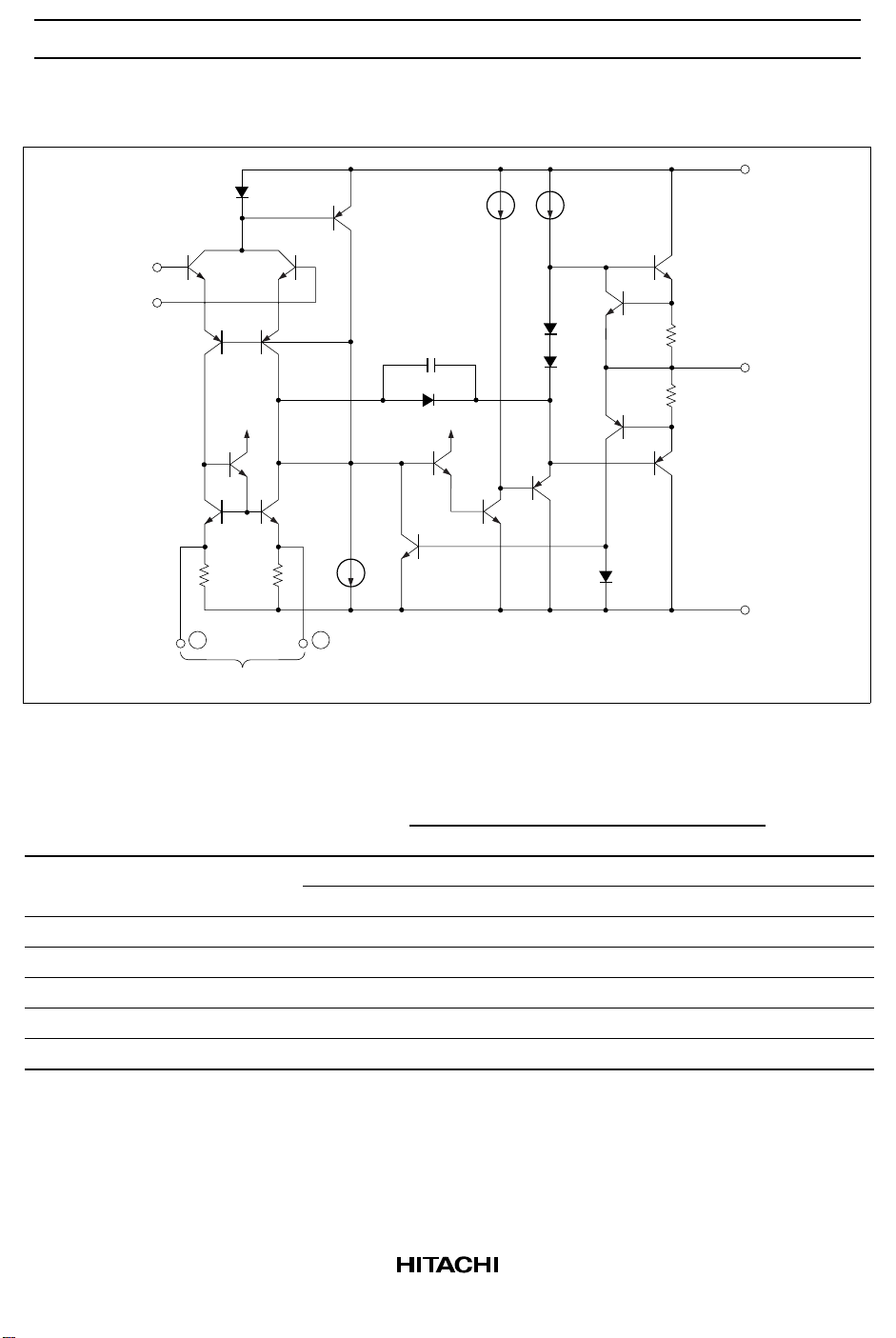
Pin Arrangement
Offset
Vin(−)
Vin(+)
Null
V
EE
1
2
3
4
−
+
(Top view)
8
7
6
5
NC
V
CC
Vout
Offset
Null

HA17741/PS
Circuit Structure
Vin(+)
Vin(−)
V
CC
Vout
To V
CC
1
Pin
5
Pin
To V
CC
V
EE
Offset Null
Absolute Maximum Ratings (Ta = 25°C)
Ratings
Item Symbol HA17741PS HA17741 Unit
Power-supply voltage V
CC
V
EE
Input voltage Vin ±15 ±15 V
Differential input voltage Vin(diff) ±30 ±30 V
Allowable power dissipation P
T
Operating temperature Topr –20 to +75 –20 to +75 °C
Storage temperature Tstg –55 to +125 –55 to +125 °C
Note: These are the allowable values up to Ta = 45°C. Derate by 8.3 mW/°C above that temperature.
+18 +18 V
–18 –18 V
670 * 670 * mW
2

HA17741/PS
Electrical Characteristics
Electrical Characteristics-1 (VCC = –VEE = 15 V, Ta = 25°C)
Item Symbol Min Typ Max Unit Test Condition
Input offset voltage V
Input offset current I
Input bias current I
IO
IO
IB
Power-supply ∆VIO/∆VCC— 30 150 µV/V RS ≤ 10 kΩ
rejection ratio ∆VIO/∆VEE— 30 150 µV/V RS ≤ 10 kΩ
Voltage gain A
Common-mode
VD
CMR 70 90 — dB RS ≤ 10 kΩ
rejection ratio
Common-mode input
V
CM
voltage range
Maximum output V
OP-P
voltage amplitude ±10 ±13 — V RL ≥ 2 kΩ
Power dissipation Pd — 65 100 mW No load
Slew rate SR — 1.0 — V/µsRL ≥ 2 kΩ
Rise time t
r
Overshoot Vover — 5.0 — % CL = 100 pF
Input resistance Rin 0.3 1.0 — MΩ
— 1.0 6.0 mV RS ≤ 10 kΩ
— 18 200 nA
— 75 500 nA
86 106 — dB RL ≥ 2 kΩ, Vout = ±10 V
±12 ±13 — V RS ≤ 10 kΩ
±12 ±14 — V RL ≥ 10 kΩ
— 0.3 — µs Vin = 20 mV, RL = 2 kΩ,
Electrical Characteristics-2 (VCC = –VEE = 15 V, Ta = –20 to +75°C)
Item Symbol Min Typ Max Unit Test Condition
Input offset voltage V
Input offset current I
Input bias current I
Voltage gain A
Maximum output
voltage amplitude
IO
IO
IB
VD
V
OP-P
— — 9.0 mV RS ≤ 10 kΩ
— — 400 nA
— — 1,100 nA
80——dBR
±10——VR
≥ 2 kΩ, Vout = ±10 V
L
≥ 2 kΩ
L
3

HA17741/PS
IC Operational Amplifier Application Examples
Multivibrator
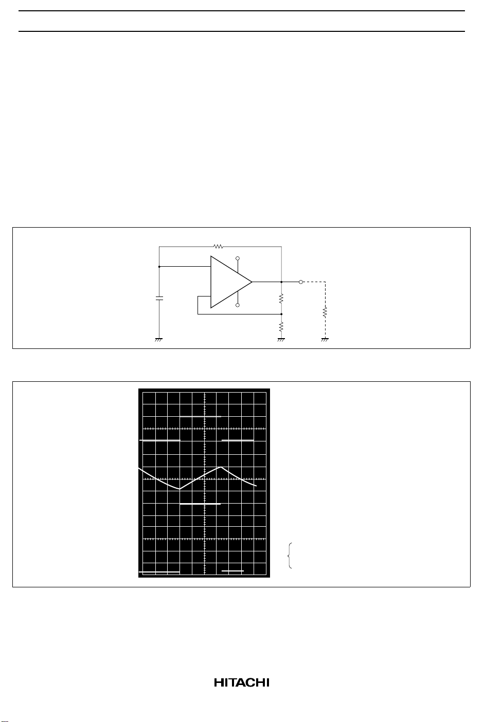
A multivibrator is a square wave generator that uses an RC circuit charge/discharge operation to generate
the waveform. Multivibrators are widely used as the square wave source in such applications as power
supplies and electronic switches.
Multivibrators are classified into three types, astable multivibrators, which have no stable states,
monostable multivibrators, which have one stable state, and bistable multivibrators, which have two stable
states.
1. Astable Multivibrator
R
3
V
Vin(−)
−
Vin(+)
C
1
+
CC
Vout
R
V
EE
1
R
L
R
2
Figure 1 Astable Multivibrator Operating Circuit
Vin(+) 0
Vin(−) 0
Vout 0
Vertical:
Horizontal:
Circuit constants
R
R
R
V
5 V/div
2 ms/div
= 8 kΩ, R2 = 4 kΩ
1
= 100 kΩ, C1 = 0.1 µF
3
= ∞
L
= 15 V, VEE = −15 V
CC
Figure 2 HA17741 Astable Multivibrator Operating Waveform
4

2. Monostable Multivibrator
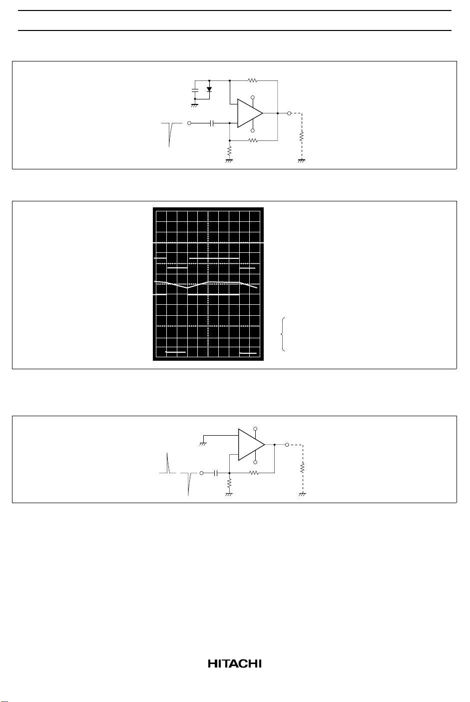
Figure 3 Monostable Multivibrator Operating Circuit
Trigger input 0
Vin(+) 0
HA17741/PS
R
3
C
1
Input
0
C
2
V
CC
−
+
R
R
2
Vout
V
EE
1
R
L
Figure 4 HA17741 Monostable Multivibrator Operating Waveform
3. Bistable Multivibrator
Vin(−) 0
Vertical:
Horizontal:
Circuit constants
= 10 kΩ, R2 = 2 kΩ
R
Vout 0
Vin(−)
Vin(+)
Input
0
C
V
−
+
V
R
L
R
2
1
= 40 kΩ, C1 = 0.47 µF
R
3
C2 = 0.0068 µF
= ∞
R
L
= 15 V, VEE = −15 V
V
CC
CC
Vout
EE
R
1
Figure 5 Bistable Multivibrator Operating Circuit
5

HA17741/PS
Trigger input 0
Vin(+) 0
Vout 0
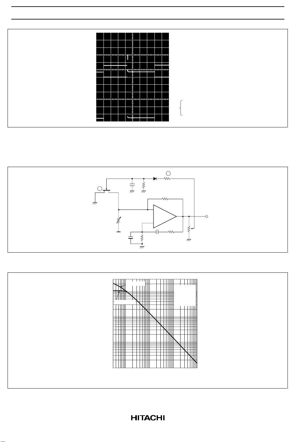
Figure 6 HA17741 Bistable Multivibrator Operating Waveform
Wien Bridge Sine Wave Oscillator
2SK16 H
Figure 7 Wien Bridge Sine Wave Oscillator
500 Ω
Rin
Vertical:
Horizontal:
5 V/div
2 ms/div
Circuit constants
R1 = 10 kΩ, R2 = 2 kΩ
C = 0.0068 µF
= ∞
R
L
= 15 V, VEE = −15 V
V
CC
1S2074 H
R
1 MΩ
R
C
3
3
4
470 kΩ
5.1 kΩ
R
S
−
+
R
C
R
2
2
1
C
1
R
Vout
50 kΩ
L
30 k
10 k
Oscillator Frequency f (Hz)
V
= 2 V
OP-P
V
= 20 V
OP-P
3 k
1 k
300
100
30
10
30 p 100 p 300 p 1,000 p 3,000 p 0.01 µ 0.03 µ 0.1 µ
VCC = 15 V,
= −15 V
V
EE
= C2/10
C
1
= 110 kΩ,
R
1
= 11 kΩ
R
2
C1 Capacitance (F)
Figure 8 HA17741 Wien Bridge Sine Wave Oscillator f–C Characteristics
6
 Loading...