HIT HA17723P, HA17723F, HA17723 Datasheet

HA17723/F/P
Precision Voltage Regulator
Description
The HA17723 high-accuracy general-purpose voltage regulator features a very low stand-by current,
(quiescent current) a low temperature drift, and high ripple rejection ratio. If you need over than 150mA
output current, adding external PNP or NPN transistor. This voltage regulator is suitable for various
applications, for example, series or parallel regulator, switching regulator.
Ordering Information
Type No. Application Package
HA17723 Commercial use DP-14
HA17723F FP-14DA
HA17723P Industrial use DP-14
Pin Arrangement
NC
CURRENT
LIMIT
CURRENT
SENSE
(–)
V
IN
V
(+)
IN
V
REF
V
EE
1
2
3
4
5
6
7
(Top View)
14
13
12
11
10
NC
COMP
V
CC
V
C
V
OUT
V
9
8
Z
NC
HA17723/F/P
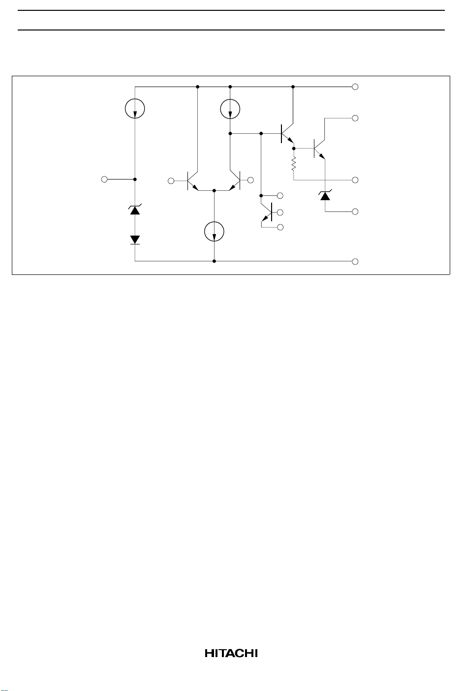
Circuit Schematic
V
REF
VIN (+)
V
CC
V
C
(–)
V
IN
V
OUT
COMP
CL
V
Z
CS
V
EE
2
HA17723/F/P
Absolute Maximum Ratings (Ta = 25°C)
Item Symbol HA17723/P HA17723F Unit
Supply voltage VCC 40 40 V
Input/Output voltage differential Vdiff (IN-O) 40 40 V
Differential input voltage VIN (diff) ±5 ±5V
Maximum output current I
Current from VREF I
Power dissipation P
OUT
REF
T
Operating temperature Topr 0 to +70 / –20 to +75 0 to +70 °C
Storage temperature Tstg –55 to +125 –55 to +125 °C
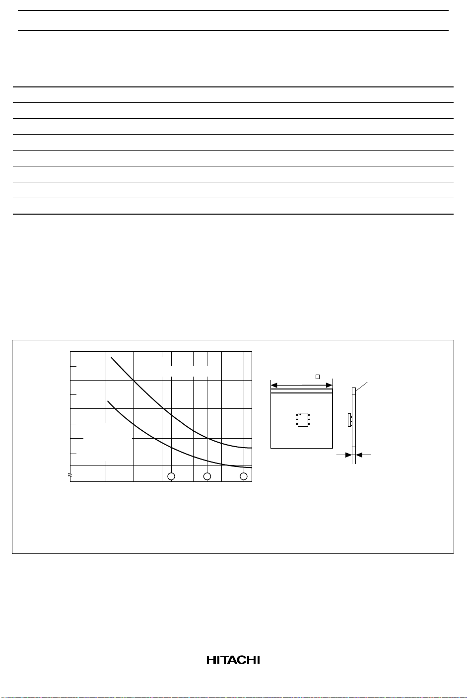
Notes: 1. Above 25°C derate by 8.3mW/°C
2. Allowable temperature of IC junction part, Tj (max), is as shown below.
Tj (max) = θj - a • Pc (max)+Ta
(θj - a is thermal resistance value during mounting, and Pc (max) is the maximum value of IC
power dissipation.)
Therefore, to keep Tj (max) ≤ 125°C, wiring density and board material must be selected
according to the board thermal conductivity ratio shown below.
Be careful that the value of Pc (max) does not exceed that P
150 150 mA
15 15 mA
830 (Note 1) 625 (Note 2) mW
.
T
240
220
SOP14
without compound
200
180
160
140
120
100
SOP14
using paste
containing
compound
80
Thermal resistance θj–a (°C/W)
21
0.5 1 2 5 10 20
Board thermal conductivity (W/m°C)
(1) Glass epoxy board with 10% wiring density
(2) Glass epoxy board with 30% wiring density
(3) Ceramic board with 96% alumina coefficient
40 mm
Board
0.8 t ceramic or
1.5 t epoxy
3
3
HA17723/F/P
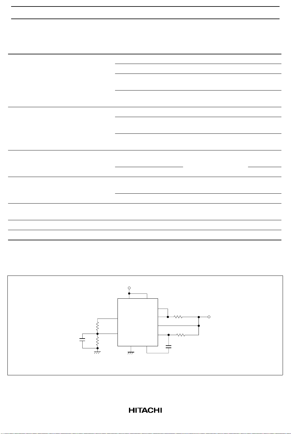
Electrical Characteristics (Ta = 25°C)
Item Symbol Min Typ Max Unit Test Conditions
Line regulation δV
Load regulation δVO Load — 0.03 0.2 % I
Ripple rejection R
Average temperature
coefficient of output voltage
Reference voltage V
Standby current I
Short circuit current limit I
Line — 0.01 0.1 % VIN = 12 to 15V
O
— 0.1 0.5 % VIN = 12 to 40V
——0.4%V
= 12 to 15V,
IN
TA = –20 to +75°C
——0.3%V
= 12 to 15V,
IN
Ta = 0 to +70°C
= 1 to 50mA
OUT
——0.7%V
= 12 to 15V,
IN
TA = –20 to +75°C
——0.6%I
= 1 to 50mA,
OUT
Ta = 0 to +70°C
REJ
— 74 — dB f = 50Hz to
10kHz
—86— C
δVO/δT — 0.003 0.018 %/°C TA = –20 to +75°C
— 0.003 0.015 %/°C Ta = 0 to +70°C
REF
ST
SC
6.80 7.15 7.50 V VIN = VCC = VC = 12V,
V
= 0
EE
— — 4.0 mA VIN = 30V, IL = 0
— 65 — mA RSC = 10Ω, V
OUT
C
= 0
REF
REF
= 0
= 5µF
Electrical Characteristics Measuring Circuit
V
IN
C
REF
VIN = VCC = VC = 12V, VEE = 0, V
RSC = 0, C1 = 100pF, C
= 0, R2 ≈ 5kΩ, R3 = R1R2/(R1+R2)
REF
4
R
1
VIN(+)
R
2
= 5.0V, IL = 1mA,
OUT
V
V
REF
V
CC
C
V
V
EE
IN
COMP
V
OUT
CL
CS
(+)
R
SC
R
3
C
1
V
OUT
HA17723/F/P
HA17723 Applications
Fixed Voltage Source in Series
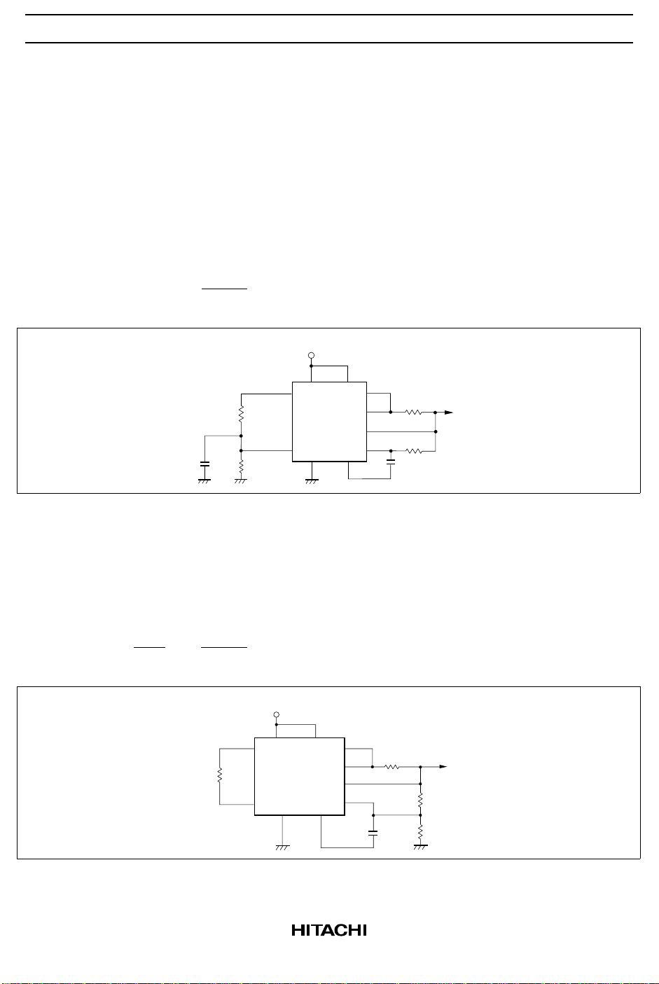
Low Voltage (2 to 7 V) Regulator: Figure 1 shows the construction of a basic low voltage regulator. The
divider (resistors R1 and R2) from V
noninverted input of the error amplifier, less than output voltage. In the fixed voltage source where the
output voltage will be fed back to the error amplifier directly as shown in figure 1. Output voltage will be
divided VREF since the output voltage is equal to the reference voltage.
makes the reference voltage, which will be provided to the
REF
Thus, the output voltage V
V
= nV
OUT
REF
OUT
, n =
C
REF
1µF
is:
R1 + R
R
2
2
R
1
2.15kΩ
R
2
4.99kΩ
V
IN
V
CC
V
REF
V
IN
(+)
V
EE
V
V
V
OUT
CL
CS
(–)
IN
COMP
C
R
= 0
R
3
SC
1.5kΩ
C
1
100pF
V
OUT
Figure 1 Low Voltage (2 to 7 V) Regulator
High Voltage (7 to 37 V) Regulator: Figure 2 shows the construction of a regulator whose output voltage
is higher than the reference voltage, V
REF
. V
is added to the non-inverted input of the error amplifier via
REF
a resistor, R3. The feedback voltage is produced by dividing the output voltage with resistors R1 and R2.
Thus, the output voltage V
V
V
OUT
REF
= , n =
n
OUT
is:
R1 + R
R
2
2
V
IN
V
V
IN
V
C
OUT
CL
CS
(–)
COMP
RSC = 0
C
1
100pF
R
3.8kΩ
V
CC
V
REF
3
V
(+)
IN
V
EE
Figure 2 High Voltage (7 to 37 V) Regulator
V
R
1
7.87kΩ
R
2
7.15kΩ
OUT
5
HA17723/F/P
Negative Voltage Regulator: Figure 3 shows the construction of a so-called negative voltage regulator,
which generates a negative output voltage with regard to GND. Assume that the output voltage, –V
increases in the negative direction. As the voltage across the R1 is larger than that across the R3, which
provides the reference voltage, the output current of the error amplifier increases. In the control circuit, the
impedance decreases with the increase of input current, which makes the base current of the external
transistor Q approach GND. As a result, the output voltage returns to the established value and output
voltage is stable.
The output voltage –VOUT of this circuit is:
OUT
,
–V
OUT
R1 + R
= –
R3 + R
= – V
R
· (R3 + R4) – R4 · (R1 + R2)
2
R
2
3
×
V
REF
R
4
1
(R1 + R2) · (R3 + R4)
V
R
2
R
3kΩ
11.5kΩ
4
V
CC
REF
×
R3 + R
V
OUT
V
V
CL
R
3
REF
4
V
C
R
5
2kΩ
Z
IN
Q
CS
VIN(+) VIN(–)
C
R
3kΩ
3
R
3.65kΩ
V
1
EE
COMP
1
100pF
V
OUT
Figure 3 Negative Voltage Regulator
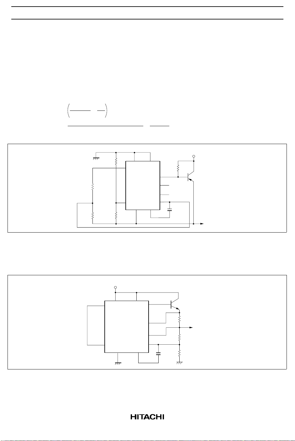
How to Increase the Output Current: To increase the output current, you must increase the current
capacity of the control circuit. Figures 4 and 5 show examples with external transistors.
V
IN
V
CC
V
REF
VIN(+) VIN(–)
V
EE
V
V
OUT
CL
CS
COMP
C
Q
R
SC
0.7Ω
V
OUT
R
1
7.87kΩ
C
500pF
R
1
2
7.15kΩ
Figure 4 Increasing Output Current (1)
6
 Loading...