HIT HA17558PS, HA17558FP, HA17558F, HA17558 Datasheet

HA17558 Serise
Dual Operational Amplifier
Description
HA17558 is dual operational amplifiers which provides internal frequency compensation and high
performance. It can be applied widely to measuring control equipment and to general Use. The two
amplifiers share a common bias network and power supply leads.
Features
• High voltage Gain: 104dB (Typ)
• High speed: 1V/µs
• Continuous short-circuit protection
• Low-noise operational amplifiers
• Internal frequency compensation
Ordering Information
Type No. Application Package
HA17558FP Industrial use FP-8D
HA17558F Commercial use FP-8D
HA17558 Commercial use DP-8
HA17558PS Industrial use DP-8

HA17558 Serise
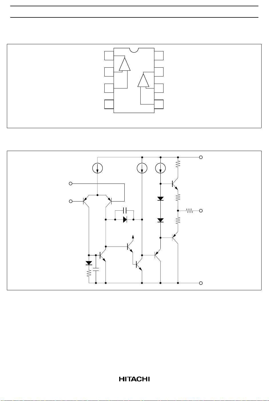
Pin Arrangement
Circuit Schematic (1/2)
Vin(+)
Vin(–)
Vout1
Vin(–)1
Vin(+)1
V
EE
1
2
3
4
1
–+
(Top View)
2
+–
8
7
6
5
V
CC
Vout2
Vin(–)2
Vin(+)2
V
CC
out
V
to V
CC
V
EE
2

HA17558 Serise
Absolute Maximum Ratings (Ta = 25°C)
Ratings
HA17558 HA17558PSHA17558FHA17558
Item Symbol
Supply voltage V
Differential input voltage V
V
CC
EE
IN (diff)
Common-mode input voltage VCM*
Power dissipation P
T
3
+18 +18 +18 +18 V
–18 –18 –18 –18 V
±30 ±30 ±30 ±30 V
±15 ±15 ±15 ±15 V
670*
Operating temperature Topr –20 to
+75
Storage temperature Tstg –55 to
+125
1
670*
–20 to
+75
–55 to
+125
1
385*
2
–20 to
+75
–55 to
+125
FP
385*
–20 to
+75
–55 to
+125
2
Notes: 1. These are the allowable values up to Ta = 45 °C. Derate by 8.3mW/°C above that temperature.
2. These are the allowable values up to Ta = 31 °C mounting on 30% wiring density glass epoxy
board. Derate by 7.14mW/°C above that temperature.
3. If the supply voltage is less than ±15V, input voltage should be less than supply voltage.
Unit
mW
–20 to
+75
°C
Electrical Characteristics (Ta = 25°C, VCC = +15V, VEE = –15V)
Item Symbol Min Typ Max Unit Test conditions
Input offset voltage V
Input offset current I
Input bias current I
Voltage gain A
IO
IO
IB
VD
Maximum output voltage Vop-p ±12 ±14 — V RL ≥ 10kΩ
Maximum output voltage Vop-p ±10 ±12.4 — V RL ≥ 2kΩ
Common mode input voltage
V
CM
range
Common mode rejection ratio CMR 70 100 — dB RS ≤ 10kΩ
Supply voltage rejection ratio PSRR — 10 150 µV/V RS ≤ 10kΩ
Power dissipation Pd — 90 170 mW 2-channel, No load
Slew rate SR — 1.0 — V/µsAVD = 1
Equivalent input noise voltage V
NI
Channel separation CS — 105 — dB f = 1kHz
— 0.5 6 mV RS ≤ 10kΩ
— 5 200 nA
— 50 500 nA
86 104 — dB RL ≥ 2kΩ, VO = ±10V
±12 ±14 — V
—6 —µVp-p RS = 1kΩ, f = 1HZ to 1kH
Z
3

HA17558 Serise
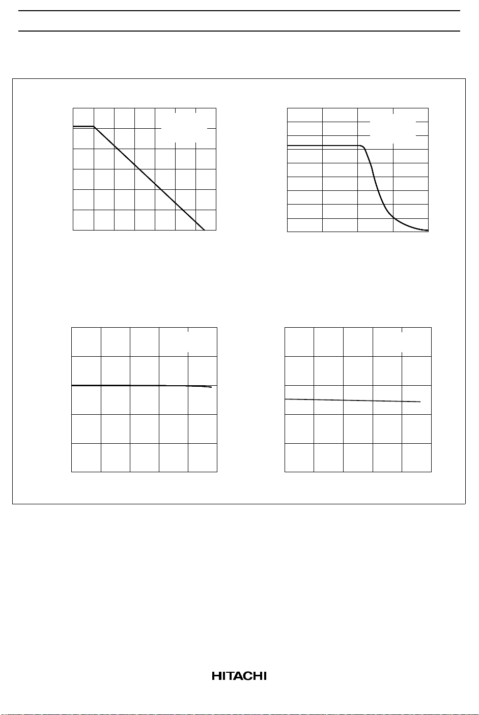
Characteristic Curves
Open Loop Voltage Gain vs. Frequency
120
(dB)
100
V(OL)
VCC = 15 V
V
EE
R
= 2 kΩ
L
80
60
40
20
0
Open Loop Voltage Gain A
1 10 100 1 k 10 k 100 k 1 M 10 M
Frequency f (Hz)
Power Supply Rejection Ratio
vs. Ambient Temperature
120
VCC = 15 V
V
110
EE
100
= –15 V
= –15 V
Maximum Output Voltage vs. Frequency
36
(V)
32
OP-P
28
VCC = 15 V
V
R
24
20
16
12
8
4
0
Maximum Output Voltage V
100
1 k 10 k 100 k 1 M
Frequency f (Hz)
Voltage Gain vs. Ambient Temperature
130
120
(dB)
VD
110
= –15 V
EE
= 2 kΩ
L
VCC = 15 V
= –15 V
V
EE
90
80
70
Power Supply Rejection Ratio PSRR (dB)
–20
0 20406080
Ambient Temperature Ta (°C)
4
100
Voltage Gain A
90
80
–20
Ambient Temperature Ta (°C)
0 20406080
 Loading...