

Page 1
Global LCD Panel Exchange Center
˖
TFT LCD Preliminary Specification
www.panelook.com
MODEL NO.
Customer:
Approved by:
Note:
HC315BH-D04
Approved By Date:
Reviewed By Date:
Prepared By Date:
1
One step solution for LCD / PDP / OLED panel application: Datasheet, inventory and accessory!
www.panelook.com
Page 2
Global LCD Panel Exchange Center
NO. ITEM PAGE
CONTENT 2
DESCRIPTION 3
1 ABSOLUTE MAXIMUM RATINGS 4
2 INITIAL OPTICAL CHARACTERISTICS 6
3 ELECTRICAL CHARACTERISTICS 9
4 BLOCK DIAGRAM 12
5 INTERFACE PIN ASSIGNMENT 13
6 MECHANICAL CHARACTERISTICS 19
7 PACKAGING 21
8 PRECAUTIONS 23
www.panelook.com
CONTENT
2
One step solution for LCD / PDP / OLED panel application: Datasheet, inventory and accessory!
www.panelook.com
Page 3

Global LCD Panel Exchange Center
www.panelook.com
DESCRIPTION
The following specifications are applied to the following Hisense module.
Product Name: HC315BH-D04
General Specifications
Effective Display Area :(H)697.6845×(V)392.256 (mm)
Number of Pixels :(H)1366×R.G..B×(V)768 (Pixels)
Pixel Pitch :(H)0.17025×(V)0.51075 (mm)
Color Pixel Arrangement : R+G+B Vertical Stripe
Display Mode : Transmissive Mode
Normally Black Mode
Top polarizer Type : Anti-Glare
Number of Colors : 16.7M (colors)
Viewing Angle Range : +88/-88(H), +88/-88(V) Typ.
Back Light : 6 CCFL
Color Chromaticity : R=0.642, 0.332
G=0.277, 0.598
B=0.145, 0.066
W=0.285, 0.293
External Dimensions : (H)760.0×(V)450.0×(D)32.5 (mm)
Weight : 6.3 (Kg)
3
One step solution for LCD / PDP / OLED panel application: Datasheet, inventory and accessory!
www.panelook.com
Page 4
Global LCD Panel Exchange Center
www.panelook.com
1. ABSOLUTE MAXIMUM RATINGS
1.1 Environment Absolute Maximum Ratings
The following items are maximum values which, if exceeded, may cause faulty operation or
damage to the LCD module.
TFT Module
Parameter Symbol
Va l ue
Min. Max.
Operating
Temperature
Storage
Temperature
Altitude
Operating
Vibration
(Non-Operating)
TOP 0 50 ć (1),(2),(3)
TST -20 60 ć (1),(3)
AOP 0 5000 M (3)
AST 0 12000 M (3)
Notes : 1) Temperature and relative humidity range is shown in the figure below.
(a) 90 %RH Max. (Taİ40 ºC).
(b) Wet-bulb temperature should be 39 ºC Max. (Ta > 40 ºC).
(c) No condensation.
Unit Note
2) The maximum operating temperature is based on the test condition that the surface
temperature of display area is less than or equal to 65 ºC with LCD module alone in a
temperature controlled chamber. Thermal management should be considered in final
product design to prevent the surface temperature of display area from being over 65 ºC.
4
One step solution for LCD / PDP / OLED panel application: Datasheet, inventory and accessory!
www.panelook.com
Page 5
Global LCD Panel Exchange Center
www.panelook.com
The range of operating temperature may degrade in case of improper thermal management
in final product design.
3) The rating of environment is base on LCD module. Leave LCD cell alone, this environment
condition can’t be guaranteed. Except LCD cell, the customer has to consider the ability
of other parts of LCD module and LCD module process.
1.2 BACKLIGHT UNIT
1.2.1 TFT LCD MODULE
ITEM Symbol
Va l ue
Unit Note
Min. Max.
Power Supply Voltage
VCC -0.3 13.0 V (1)
1.2.2 BACKLIGHT UNIT
ITEM Symbol
Va l ue
Unit Note
Min. Max.
Lamp Voltage Vw - 3000 VRMS
Power Supply Voltage VBL 0 30 V (1)
Control Signal Level -0.3 7 V (1),(3)
Note (1) Permanent damage to the device may occur if maximum values are exceeded. Functional
operation should be restricted to the conditions described under normal operating conditions.
Note (2) No moisture condensation or freezing.
Note (3) The control signals includes Backlight On/Off Control, I_PWM Control, E_PWM Control and
ERR signal for inverter status output.
5
One step solution for LCD / PDP / OLED panel application: Datasheet, inventory and accessory!
www.panelook.com
Page 6
Global LCD Panel Exchange Center
www.panelook.com
2. INITIAL OPTICAL CHARACTERISTICS
The following optical characteristics are measured under stable conditions. It takes about 30 minutes to
reach stable conditions. The measuring point is the center of display area unless otherwise noted. The
optical characteristics should be measured in a dark room or equivalent state.
Measuring equipment˖SR-3 and LIPS
Ambient Temperature=25±2°C, V
=12.0V, fV=60Hz, Dclk=74.25MHz V
LCD
Item Symbol Condition Min. Typ. Max. Unit Note
Red
Green
Color
Chromaticity
Blue
white
Center Transmittance T% - 5.8 ˁ (1),(7)
Contrast Ratio CR
Response Time
White Variation W x=0°, y=0° 1.5 - (1),(6)
Horizontal
Viewing
Angle
Vertical
x 0.652
y 0.332
x 0.277
y 0.598
x 0.145
y 0.066
x=0°, y=0° viewing
angle at normal
direction
Typ.- 0.03
x 0.285
y
0.293
x=0°, y=0°
2000 3000 - (1),(3)
Gray to
gray
average
+
80 88 -
X
-
X
+
80 88 -
Y
-
Y
x=0°, y=0° with
Module@60Hz
CRı20
- 6.5 12 ms (4)
80 88 -
80 88 -
Note (1) Driving voltages are based on suitable gamma voltages.
The calculated method is as following:
1. Measure module’s and backlight’s spectrum. White and R, G, B are with signal input.
2. Calculate cell’s spectrum.
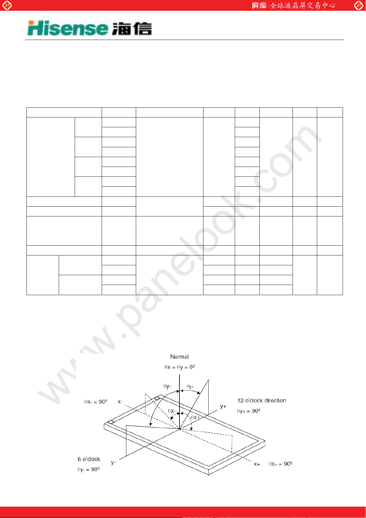
Note (2) Definition of Viewing Angle (x, y):
Viewing angles are measured by EZ-Contrast 160R (Eldim)
=1.65V, EXTV
BR_A
Typ.+0.03 - (1),(5)
Deg. (1),(2)
BR_B
=100%
6
One step solution for LCD / PDP / OLED panel application: Datasheet, inventory and accessory!
www.panelook.com
Page 7
Global LCD Panel Exchange Center
www.panelook.com
Note (3) Definition of Contrast Ratio (CR):
The contrast ratio can be calculated by the following expression.
Contrast Ratio (CR) = L255 / L0
L255: Luminance of gray level 255
L 0: Luminance of gray level 0
CR = CR (5), where CR (X) is corresponding to the Contrast Ratio of the point X at the figure
in Note (6).
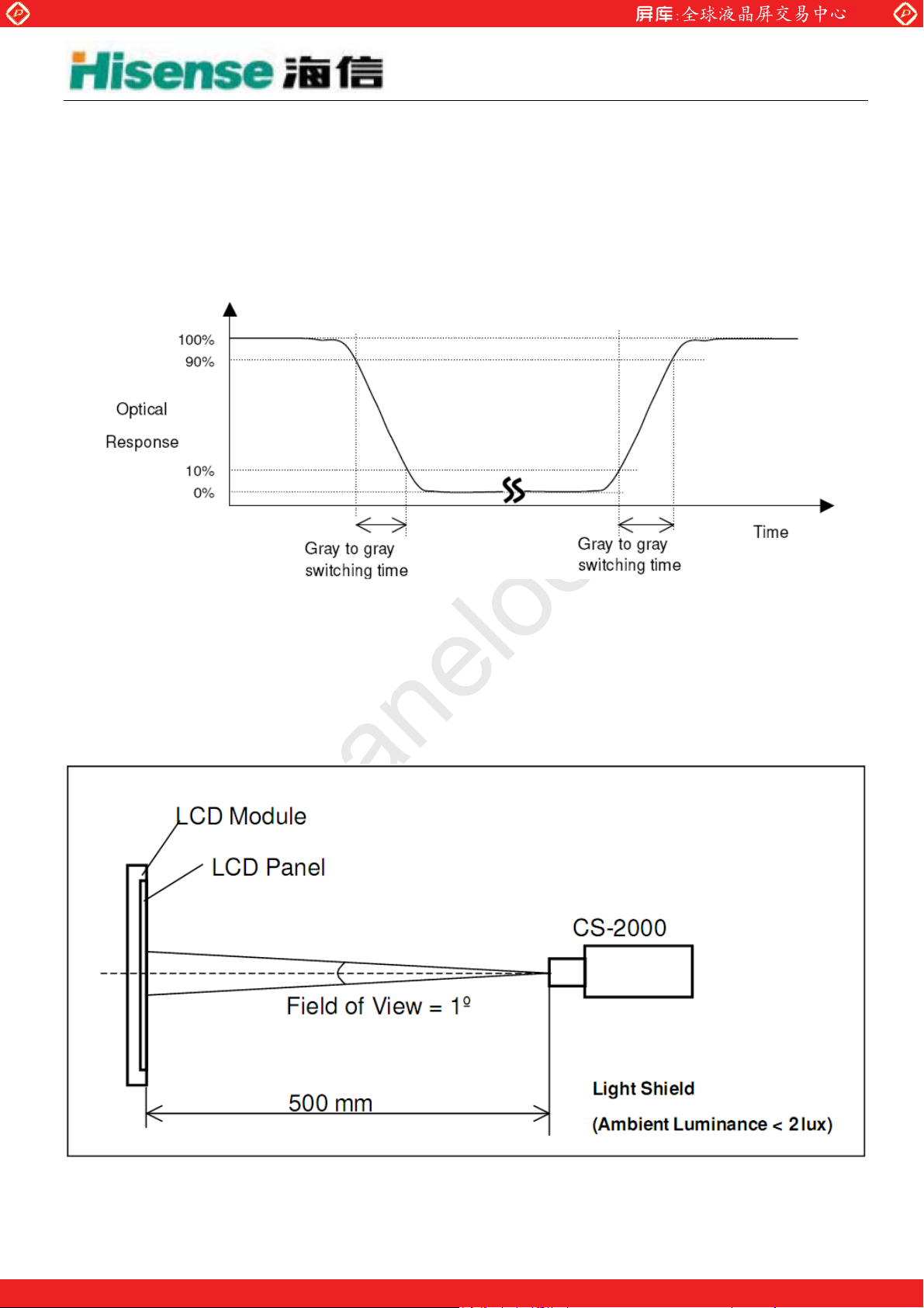
Note (4) Definition of Gray to Gray Switching Time:
The driving signal means the signal of gray level 0, 123, 168, 202, 230, 255. Gray to gray average
time means the average switching time of gray level 0, 123, 168, 202, 230, 255 to each other.
Note (5) Measurement Setup:
The LCD module should be stabilized at given temperature for 60 minutes to
avoid abrupt temperature change during measuring. In order to stabilize the luminance,
the measurement should be executed after lighting Backlight for 60 minutes in a windless room.
7
One step solution for LCD / PDP / OLED panel application: Datasheet, inventory and accessory!
www.panelook.com
Page 8

Global LCD Panel Exchange Center
Note (6) Definition of White Variation (W):
Measure the luminance of gray level 255 at 5 points
W = Maximum [L (1), L (2), L (3), L (4), L (5)] / Minimum [L (1), L (2), L (3), L (4), L (5)]
where L (X) is corresponding to the luminance of the point X at the figure below.
www.panelook.com
Note (7) Definition of Transmittance (T%):
Module is without signal input.
8
One step solution for LCD / PDP / OLED panel application: Datasheet, inventory and accessory!
www.panelook.com
Page 9

Global LCD Panel Exchange Center
3. ELECTRICAL CHARACTERISTICS
3.1 TFT-LCD Module
www.panelook.com
Parameter Symbol
Va l ue
Min. Typ. Max.
Power Supply Voltage VCC 11.4 12.0 12.6 V (1)
Rush Current I
- - 3.4 A (2)
RUSH
White - 0.45 0.52 A
Power Supply
Current
Black - 0.33 - A
Vertical
Stripe
I
CC
- 0.45 - A
Differential input
High Threshold
V
- - +100 mV
LV TH
Voltage
Differential input
LVDS
Low Threshold
Voltage
V
-100 - - mV
LV TL
Interface
Common input
Voltage
VCM 1.0 1.2 1.4 V
Terminating Resistor RT - 100 - ohm
CMOS
Interface
Differential input
voltage
Input High
Threshold Voltage
Input Low
Threshold Voltage
| 200 - 600 mV
|V
ID
VIH 2.7 - 3.3 V
0 - 0.7 V
V
IL
Note (1) The module should be always operated within above ranges.
Unit Note
(3)
9
One step solution for LCD / PDP / OLED panel application: Datasheet, inventory and accessory!
www.panelook.com
Page 10

Global LCD Panel Exchange Center
Note (2) Measurement Conditions:
www.panelook.com
10
One step solution for LCD / PDP / OLED panel application: Datasheet, inventory and accessory!
www.panelook.com
Page 11

Global LCD Panel Exchange Center
www.panelook.com
Note (3) The specified power supply current is under the conditions at Vcc =12V, Ta = 25 ± 2 ºC, fv = 60
Hz, where as a power dissipation check pattern below is displayed.
Note (4) The LVDS input characteristics are as follows:
11
One step solution for LCD / PDP / OLED panel application: Datasheet, inventory and accessory!
www.panelook.com
Page 12

Global LCD Panel Exchange Center
4. BLOCK DIAGRAM
4.1 TFT Module
www.panelook.com
12
One step solution for LCD / PDP / OLED panel application: Datasheet, inventory and accessory!
www.panelook.com
Page 13

Global LCD Panel Exchange Center
5. INTERFACE PIN ASSIGNMENT
5.1 TFT-LCD MODULE
CNF1 Connector Pin Assignment
Pin No. Symbol Description Note
1 VCC Power supply: +12V
2 VCC Power supply: +12V
3 VCC Power supply: +12V
4 VCC Power supply: +12V
5 GND Ground
6 GND Ground
7 GND Ground
8 GND Ground
9 SELLVDS Select LVDS data format (2)
10 ODSEL Overdrive Lookup Table Selection (3)
11 GND Ground
12 RX0- Negative transmission data of pixel 0
13 RX0+ Positive transmission data of pixel 0
14 GND Ground
15 RX1- Negative transmission data of pixel 1
16 RX1+ Positive transmission data of pixel 1
17 GND Ground
18 RX2- Negative transmission data of pixel 2
19 RX2+ Positive transmission data of pixel 2
20 GND Ground
21 RXCLK- Negative of clock
22 RXCLK+ Positive of clock
23 GND Ground
24 RX3- Negative transmission data of pixel 3
25 RX3+ Positive transmission data of pixel 3
26 GND Ground
27 TST_AGE Aging Mode (4)
28 NC No connection (5)
29 GND Ground
30 GND Ground
Note (1) Connector type: STARCONN 093G30-B0001A or P-TWO 187053-30091or compatible
LVDS connector pin orderdefined as follows
www.panelook.com
Note (2) Low = Open or connect to GND: VESA Format, High = Connect to +3.3V: JEIDA Format.
Please refer to 5.5 LVDS INTERFACE
13
One step solution for LCD / PDP / OLED panel application: Datasheet, inventory and accessory!
www.panelook.com
Page 14

Global LCD Panel Exchange Center
Note (3) Overdrive lookup table selection. The Overdrive lookup table should be selected in
accordance to the frame rate to optimize image quality.
Low = Open or connect to GND, High = Connect to +3.3V
ODSEL Note
L or Open Lookup table was optimized for 60 Hz frame rate
H Lookup table was optimized for 50 Hz frame rate
Note (4) Ground or OPEN: Disable, High: Enable.
Note (5) Reserved for internal use. Left it open.
Note (6) LVDS signal pin connected to the LCM side has the following diagram.
R1 in the system side should be less than 1K Ohm. (R1 < 1K Ohm)
www.panelook.com
14
One step solution for LCD / PDP / OLED panel application: Datasheet, inventory and accessory!
www.panelook.com
Page 15

Global LCD Panel Exchange Center
www.panelook.com
5.2 RELATIONSHIP BETWEEN DISPLAY COLORS AND INPUT SIGNALS
The brightness of each primary color(red,green,blue) is based on the 8-bit gray scale data input for
the color. The higher binary input, the brighter the color. The table below provides the assignment of
color versus data input.
15
One step solution for LCD / PDP / OLED panel application: Datasheet, inventory and accessory!
www.panelook.com
Page 16

Global LCD Panel Exchange Center
www.panelook.com
5.4. Signal Timing Specifications
The following table shows the signal timing required at the input of the LVDS transmitter. All of the
interface signal timing should be satisfied with the following specification for normal operation.
Signal Item Symbol Min. Typ. Max. Unit Note
Frequency 1/Tc 60 76 82 MHz
LVDS Receiver Clock
Input cycle to cycle
jitter
Spread spectrum
modulation range
Trcl - - 200 ps (3)
F
clkin_modFclkin
-ˁ - F
+ˁ MHz
clkin
Spread spectrum
modulation
200 KHz
F
SSM
frequency
LVDS Receiver Data
Setup Time Tlvsu 600 - - ps
Hold Time Tlvhd 600 - - ps
Frame Rate
Fr5 47 50 53 Hz
Fr6 57 60 63 Hz
Vertical Active Display
Term
Total Tv 778 806 888 Th Tv=Tvd+Tvb
Display Tvd 768 768 768 Th -
Blank Tvb 10 38 120 Th -
Total Th 1442 1560 1936 Tc Th=Thd+Thb
Horizontal Active Display
Term
Display Thd 1366 1366 1366 Tc -
Blank Thb 76 194 570 Tc -
Note (1) Please make sure the range of pixel clock has follow the below equation:
Fclkin(maxı)Uh7Yh7K
)Uh7Yh7Kı)FONLQPLQ
Note(2) This mode is operated in DE only mode and please follow the input signal timing diagram below:
(4)
(5)
(2)
16
One step solution for LCD / PDP / OLED panel application: Datasheet, inventory and accessory!
www.panelook.com
Page 17

Global LCD Panel Exchange Center
www.panelook.com
Note (3) The input clock cycle-to-cycle jitter is defined as below figures. Trcl = |T1 – T|
Note (4) The SSCG (Spread spectrum clock generator) is defined as below figures.
Note (5) The LVDS timing diagram and setup/hold time is defined and showing as the following figures.
17
One step solution for LCD / PDP / OLED panel application: Datasheet, inventory and accessory!
www.panelook.com
Page 18

Global LCD Panel Exchange Center
5.5. Power On/Off Sequence
www.panelook.com
18
One step solution for LCD / PDP / OLED panel application: Datasheet, inventory and accessory!
www.panelook.com
Page 19

Global LCD Panel Exchange Center
6. MECHANICAL CHARACTERISTICS
www.panelook.com
19
One step solution for LCD / PDP / OLED panel application: Datasheet, inventory and accessory!
www.panelook.com
Page 20

Global LCD Panel Exchange Center
www.panelook.com
20
One step solution for LCD / PDP / OLED panel application: Datasheet, inventory and accessory!
www.panelook.com
Page 21

Global LCD Panel Exchange Center
7. PACKAGING
7.1 PACKAGING SPECIFICATION
(1) 5 LCD TV modules / 1 Box
(2) Box dimensions : 826(L)x376(W)x540(H)mm
(3) Weight : approximately 50Kg (5 modules per box)
7.2 PACKAGING METHOD
Figures 7-1 and 7-2 are the packing method
www.panelook.com
Figure.7-1 packing method
21
One step solution for LCD / PDP / OLED panel application: Datasheet, inventory and accessory!
www.panelook.com
Page 22

Global LCD Panel Exchange Center
www.panelook.com
Figure.7-2 packing method
22
One step solution for LCD / PDP / OLED panel application: Datasheet, inventory and accessory!
www.panelook.com
Page 23

Global LCD Panel Exchange Center
www.panelook.com
8. PRECAUTIONS
8.1 ASSEMBLY AND HANDLING PRECAUTIONS
1) Do not apply rough force such as bending or twisting to the module during assembly.
2) It is recommended to assemble or to install a module into the user’s system in clean working areas.
The dust and oil may cause electrical short or worsen the polarizer.
3) Do not apply pressure or impulse to the module to prevent the damage of LCD panel and
backlight.
4) Always follow the correct power-on sequence when the LCD module is turned on. This can
prevent the damage and latch-up of the CMOS LSI chips.
5) Do not plug in or pull out the I/F connector while the module is in operation.
6) Do not disassemble the module.
7) Use a soft dry cloth without chemicals for cleaning, because the surface of polarizer is very soft
and easily scratched.
8) Moisture can easily penetrate into LCD module and may cause the damage during operation.
9) High temperature or humidity may deteriorate the performance of LCD module. Please store LCD
modules in the specified storage conditions.
10) When ambient temperature is lower than 10ºC, the display quality might be reduced. For
example, the response time will become slow, and the starting voltage of CCFL will be higher than
that of room temperature.
8.2 SAFETY PRECAUTIONS
1) The startup voltage of a backlight is over 1000 Volts. It may cause an electrical shock while
assembling with the inverter. Do not disassemble the module or insert anything into the backlight unit.
2) If the liquid crystal material leaks from the panel, it should be kept away from the eyes or mouth.
In case of contact with hands, skin or clothes, it has to be washed away thoroughly with soap.
3) After the module’s end of life, it is not harmful in case of normal operation and storage.
8.3 STORAGE PRECAUTIONS
When storing modules as spares for a long time, the following precaution is necessary. 1) Do not
leave the module in high temperature, and high humidity for a long time. It is highly
recommended to store the module with temperature from 0 to 35ćat normal humidity without
condensation.
2) The module shall be stored in dark place. Do not store the TFT-LCD module in direct sunlight or
fluorescent light.
23
One step solution for LCD / PDP / OLED panel application: Datasheet, inventory and accessory!
www.panelook.com
 Loading...