


Instruction Manual
SM7860-01 to -07
SM7860-21 to -27
POWER SOURCE UNIT
February 2012 Revised edition 1 SM7860A981-01 12-02H


Contents
Introduction.................................................................................1
i
Contents
1
Confirming Packa g e Co n te n ts.............. .. ... .. ... ..................... ... .. ..1
Safety Informa tion ............. .. ... .. .. ...................... .. ... .. ...................2
Operating Precautions................................................................3
Chapter 1
Overview___________________________________ 7
1.1 Product Overview and Features .........................................7
1.2 Names and Functions of Parts ............................................8
1.3 Screen Layout ...................................................................10
Chapter 2
Preparing to Use the Device and
Supplying Power ___________________________ 11
2.1 Installation & Connection Procedures ...............................11
2.2 Connecting the Power Cord ..............................................12
2.3 Connecting the Device to the Measuring Instrument ........13
2
3
4
5
6
7
2.4 Pre-Operation Inspection ..................................................14
2.5 Turning the Power On and Off ..........................................15
2.6 Setting the Operating Conditions ......................................16
Chapter 3
Communication (GP-IB/RS-232C Interface)______ 17
3.1 Overview and Features .....................................................17
3.2 Specifications ............................................................ ........ 18
3.3 Connect a cable to the GP-IB
connector or RS-232C connector 19
3.4 Configuring the Communications Protocol ........................21
3.5 Communication Methods ..................................................22
Status Byte Register .........................................................................24
Eve n t R e g is te rs ..... ... ..................................... ...................................2 6
Error Registers ..................................................................................28
3.6 Message List .....................................................................29
3.7 Listener Specification Precautions ....................................32
Input buffer size ................................................................................32
Reading from the output buffer .........................................................32
8
9
10
11
12
付
録
索
引

ii
Contents
Chapter 4
External Control ____________________________33
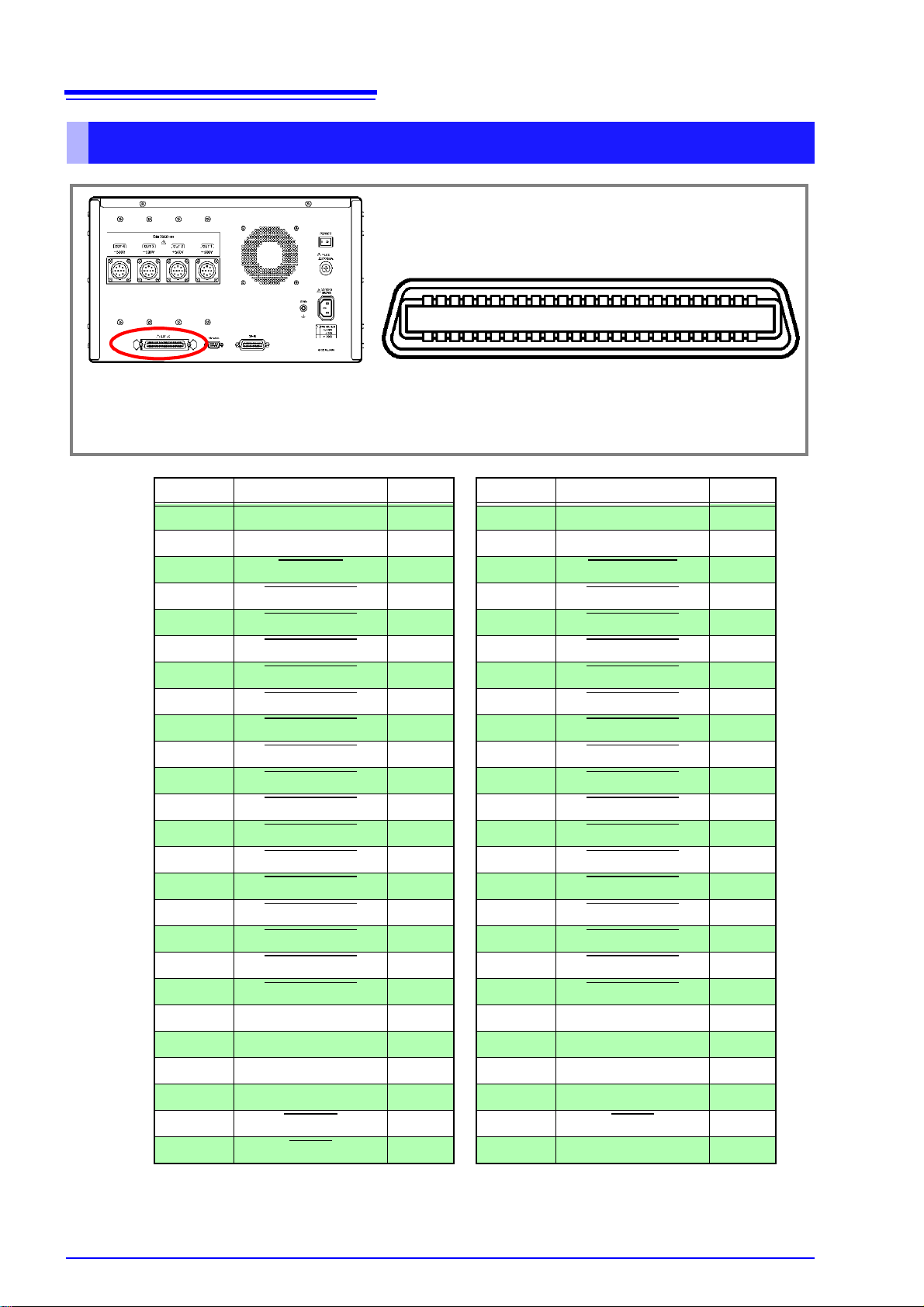
4.1 External Input/Output Connector and Signals ..................33
Connector Type and Signal Pinouts .................................................34
Signal Descriptions ..........................................................................35
4.2 Timing Chart .....................................................................36
4.3 Internal Circuitry ................................................................38
Chapter 5
Specifications______________________________39
5.1 General Specifications ......................................................39
5.2 Basic Specifications ..........................................................40
5.3 Input / Output Functions ...................................................44
Chapter 6
Maintenance and Service ____________________45
6.1 Troubleshooting ................................................................ 45
Inspection and Repair ......................................................................45
6.2 Replacing the Power Fuse ................................................47
6.3 Error Displays ...................................................................48
6.4 Cleaning .................................................... ........................48
Introduction
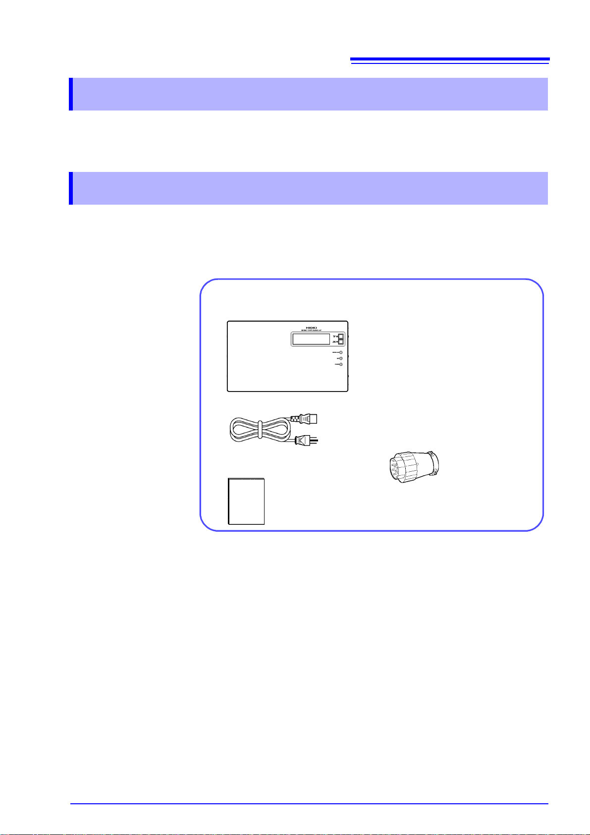
Confirm that th e se contents are provided.
□ SM7860 series Power Source Unit (1)
□ Power Cord (1)
□ Instruction Manual (1)
□ Voltage output connector
SM7860-01, -02, -21, -22.............2
SM7860-03, -04, -05, -06, -07,
-23, -24, -25, -26, -27 ......4
Thank you for purchas ing the HIOKI Model SM7860 series Power Source Unit.
To obtain maximum performance from the devic e, please read this manu al first,
and keep it handy for future reference.
Confirming Package Contents
When you receive the device, inspect it carefully to ensure that no damage
occurred during shipp ing. In particular, check the accessor ies, panel switches,
and connectors . If damage is evident, or if it fa ils to operate according to the
specifications, contact your dealer or Hioki representative.
1
Introduction
Options □ Model 9637 RS-232C Cable (9pin-9pin/Cross/1.8m)
Transportation
Notes on
□ Model 9638 RS-232C Cable (9pin-25pin/Cross/1.8m)
□ Model 9151-02 GP-IB Connector Cable (2 m)
• To ensure safe handling, when transporting the device, please use the original
box and packing materials, but do not use if the box is damaged or warped, or
if the packing materials are in poor condition or incomple te.
• When packing the device, m ake sure to disconnec t the power c ords from t he
main device.
• When transporting, avoid dropping or other excessive impact.

2
Safety Information
Safety Information
This device is des igned to comply with IEC 61010 Safety Standards, and
has been thoroughly tested for safety prior to shipment. However, mishandling during use could result in injury or death, as well as damage to the
device. Using the device in a way not described in this manual may negate
the provided safety features.
Be certain that you understand the instructions and precautions in the
manual before use. We disclaim any responsibility for accidents or injuries
not resulting directly from device defects.
This manual contain s information and warnings essential for safe operation of
the device and for maintaining it in safe operati ng condition. Be fore using it, b e
sure to carefully read the following safety precautions.
Safety Symbols
In the manual, the symbol indicates particularly important information that
the user should read before using the device.
The symbol printed on the device indicates that the user should refer to a
corresponding topic in the manual (marked with the symbol) before using
the relevant function.
Indicates a grounding termi nal.
Indicates DC (Direct Current).
Indicates AC (Alternating Current).
Indicates the ON side of the power switch.
Indicates the OFF side of the power switch.
The following symbols in this manual indicate the relative importance of cautions
and warnings.
Indicates that incorrect operation presents an extreme hazard that
could result in serious injury or death to the user.
Indicates that incorrect operation presents a significant hazard that
could result in serious injury or death to the user.
Indicates that incor rect operatio n presen ts a po ssib ility of injury to the
user or damage to the device.
Indicates advisory items related to performance or correct operation
of the device.
Other symbols
*
PA GE UP
(Bold)
( p. )
Indicates a prohibited action.
Indicates that descriptive information is provided below.
Bold characters within the text indicate operating key labels.
Indicates the location of reference information.
Operating Precautions
Follow these precaut ions to ensure s afe ope ration an d to obta in the fu ll bene fits
of the various functions.
Preliminary Checks
Before using the device for the first time, verify that it operates normally to
ensure that no damage occurred during storage or shipping. If you find any damage, contact your dealer or Hioki representative.
Device Installation
Operating temperature and humidity
Temperature and humidity range for guaranteed accuracy
3
Operating Precautions
: 0 to 40°C at 80%RH or less (non-condensing)
: 23±5°C, 80%RH or less (non-condensing)
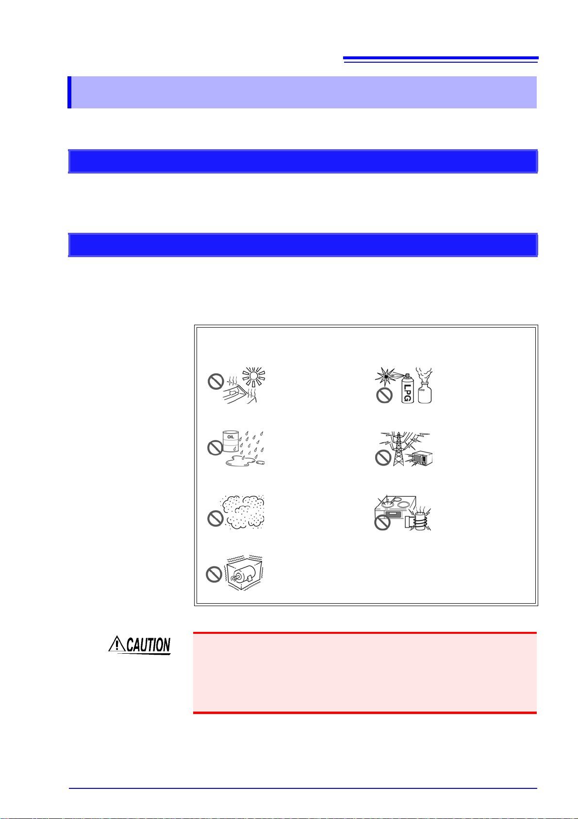
Avoid the following locations that could cause an accident or damage
to the device.
Exposed to direct sunlight
Exposed to high temperature
Exposed to water, oil,
other chemicals, or
solvents
Exposed to high humidity or condensation
Exposed to high levels of particulate dust
Subject to vibration
In the presence of corrosive or explos ive gas es
Exposed to strong electromagnetic fields
Near electromagnetic
radiators
Near electromagnetic
radiators (e.g., high-frequency induction heating systems and IH
cooking utensils)
• Do not slant the device or place it on top of an uneven surfa ce. Dropping or
knocking down the device can cause injury or damage to the device.
• Ventilation holes for heat radiation are provided on the si de and re ar panels of
the device. Leave sufficient space aroun d the ventilation holes and install t he
device with the holes unobstructed. Installation o f the device with the venti lation holes obstructed may cause a malfunction or fire.
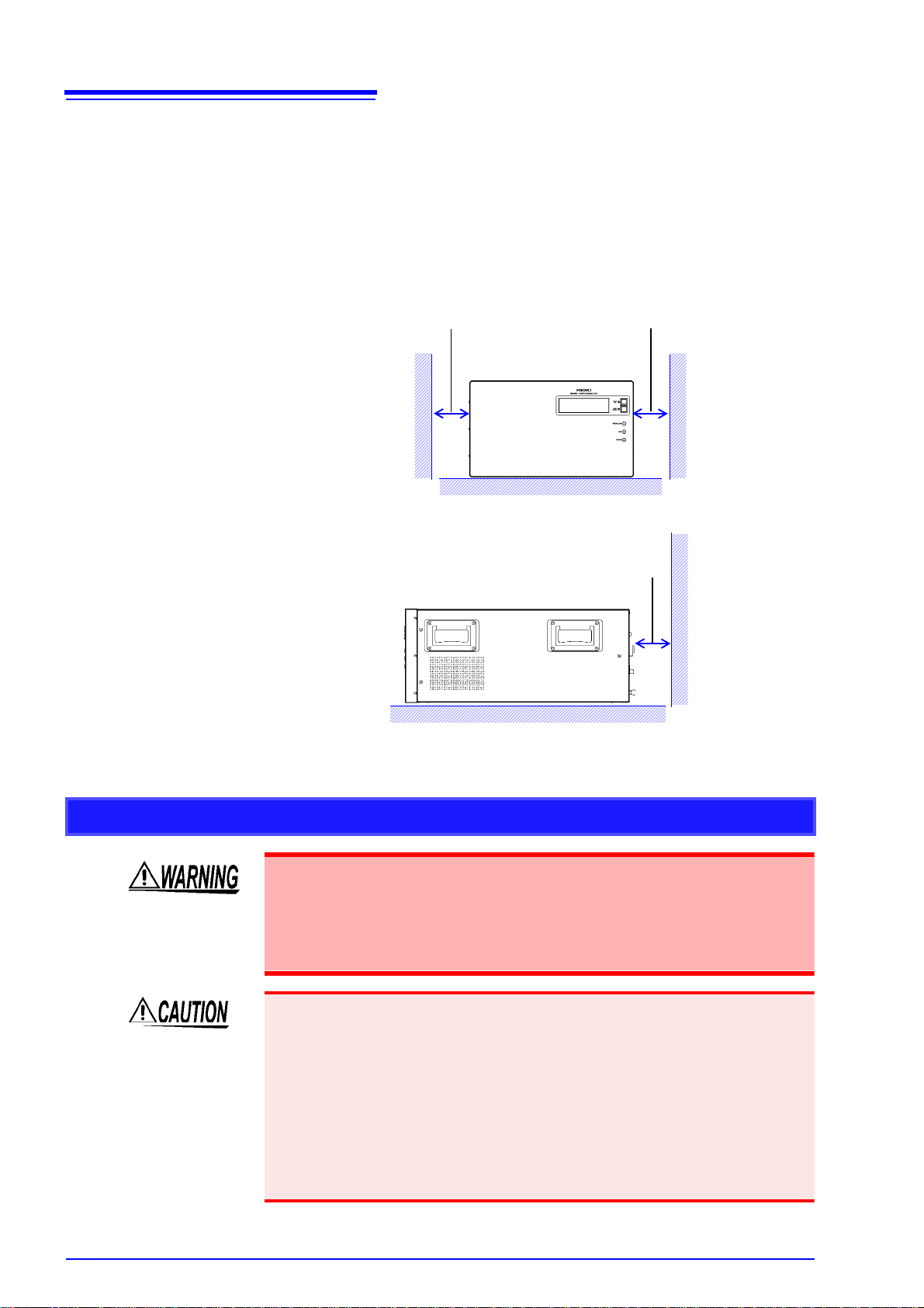
4
100 mm or more
50 mm or more
50 mm or more
Operating Precautions
Installing To prevent overheating, be sure to leave the specified clearances around the
unit.
• Vents must not be obstructed.
• When rack-mounting the dev i ce, fans must be in stalle d abov e or on top of the
rack to ensure proper ventila tion. Be sure that the rack is adequately ven tilated so that the i nternal temperature remains at o r below 40°C. Continued
use of the device in a high-temperature envir onment will shorten its servic e
life. Keep the temperature as low as possible.
Handling the Device
• Do not allow the device to get wet, and do not take measurements with
wet hands. This may cause an electric shock.
• Touching any of the high-voltage points inside the device is very danger-
ous. Do not attempt to modify, disassemble or repair the device; as fire,
electric shock and injury could result.
• To avoid damage to the device, protec t it from physic al shock whe n transport-
ing and handling. Be especially careful to avoid physical shock from dropping.
Failure to observe the following precaution may result in bodily injury.
• The device weighs approxi mately 45 kg (SM7860-07, -27: approximately 32
kg). It should be move d by at least two people, who should grip it using the
handles on the left and right sides.
• The device is he avy. When transporting it, foll ow your company's workplace
safety standards to assure safety (for example, by wearing non-slip gloves and
protective footwear).

Handling the Cords
5
Operating Precautions
Before using the device, make sure that the insulation on the Connection
Cable is undamaged and that no bare conductors are improperly exposed.
Using the de v i ce i n s u c h conditions could cause an e lec t r i c shock, so con tact your dealer or Hioki representative for replacements.
• Avoid stepping on or pinching cab les, which could damage the cable insulation.
• To avoid breaking the cables, do not bend or pull them.
• To avoid damaging the power cord, grasp the plug, not the cord, when unplugging it from the power outlet.
• Keep the cables we ll away from heat sources, as bare c onductors could be
exposed if the insulation melts.
Use only the specified connection cables. Using a non-specified cable may
result in incorrect measurements due to poor connection or other reasons.
Before Connecting
• Before turning the device on, make sure the supply voltage matches that
indicated on its power connector. Connection to an improper supply voltage may damage the device and present an electrical hazard.
• To avoid electrical accidents and to maintain the safety speci ficat ion s of
this device, connect the power cord only to a 3-contact (two-conductor +
ground) outlet.
T o ensure measurements are accurate,
• Warm up the device an hour or more before use.
• The device should be calibrated once a year.

6
Operating Precautions

1.1 Product Overview and Features
Overview Chapter 1
1.1 Product Overview and Features
The SM7860-01 to -07 and SM786 0-21 to -27 ar e power supp ly units d esigned
for use with the Model SM7810 or SM7810-20 Super MΩ HiTester. They support
bipolar, multi-channel output and are compatible with multi-channel systems.
Used in combination with the Model SM7810 or SM7810-20 Super MΩ HiTester,
they are ideal for use in automated testing and measurement of capacitors.
Bipolar, multi-channel output
The device delive rs an 8-channel, positive/negative power supply, allowing an
optimized test ing line to be built using th e smallest possible number of power
supplies.
7
Independent on/off output switching and current limitations
for all channels
Since each channel has its own output on/off switch, it is possible to control voltage application without an external circuit (allowing charging and dis charging).
Use of semiconduc tor switches elimina tes the need for mainten ance. Additionally, the ability to limit current (to 50 mA) for individual channels means the measurement of other channe ls won't be affected when a target workpiece has a
short.
Output current capacity: 50 mA/channel
High-capacity capacitors can be charged rapidly, and the number of charges can
be reduced.
Output voltage: 1,000 V/channel
Devices are available with output voltages of up to ±1,000 V.
Standard interfaces
Devices ship standard with external I/O, GP-IB, and RS-232C interfaces for
sequencing. Interfaces are used to configure and power the devices.
Inter-lock Function

8
LCD screen
The screen uses a 2-page
layout to display setting values and setting status inf ormation.
"1.3 Screen Layout" (p.10)
Front Panel
Scroll keys (PAGE UP▲/ PAGE DOWN▼)
Used to scroll through the display pages.
"1.3 Screen Layout" (p.10)
The scroll keys are also used to se t the GP-IB add ress.
(p.21)
Inter-lock indicator
Lights up when the interlock is
on.
V oltage output indicator
Lights up when a voltage is being output.
Power indicator
Lights up when the d evi ce is on.
Rear Panel
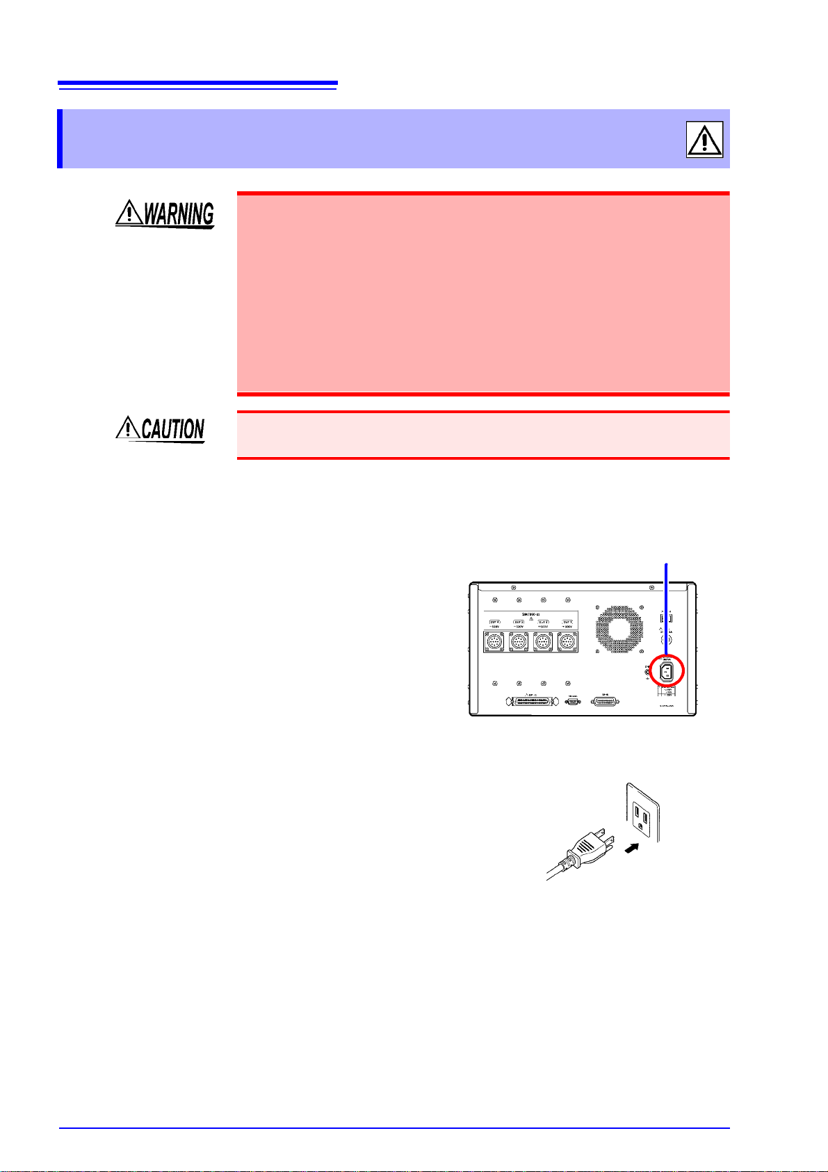
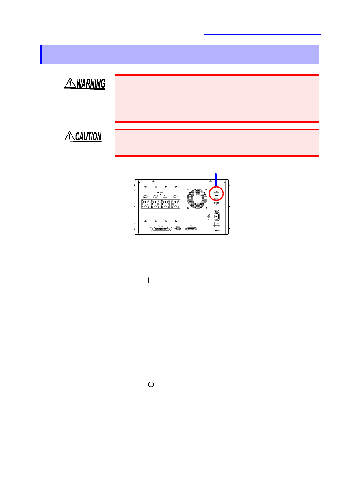
Power inlet
Connect the supplied power cord
here. (p.12)
Fuse holder
Allows the fuse to be replaced.
(p.47)
RS-232C connector
Connect to a compute r when
using the RS-232C interface.
(p.19)
EXT I/O connector
The external I/O connector
can be used to control the
device.
(p.33)
Voltage output terminal
Connect the included voltage
output connector.
(p.13)
Vent
Keep clear of obstructions.
POWER switch
Turns the device o n and off .
: Power On
: Power Off
(p.15)
GP-IB connector
Connect to a compu ter whe n using the
GP-IB interface.
(p.19)
GND terminal
Serves as the ground terminal.
The GND terminal is connected
to the device’s enclosure.
1.2 Names and Functions of Parts
1.2 Names and Function s of Parts
9
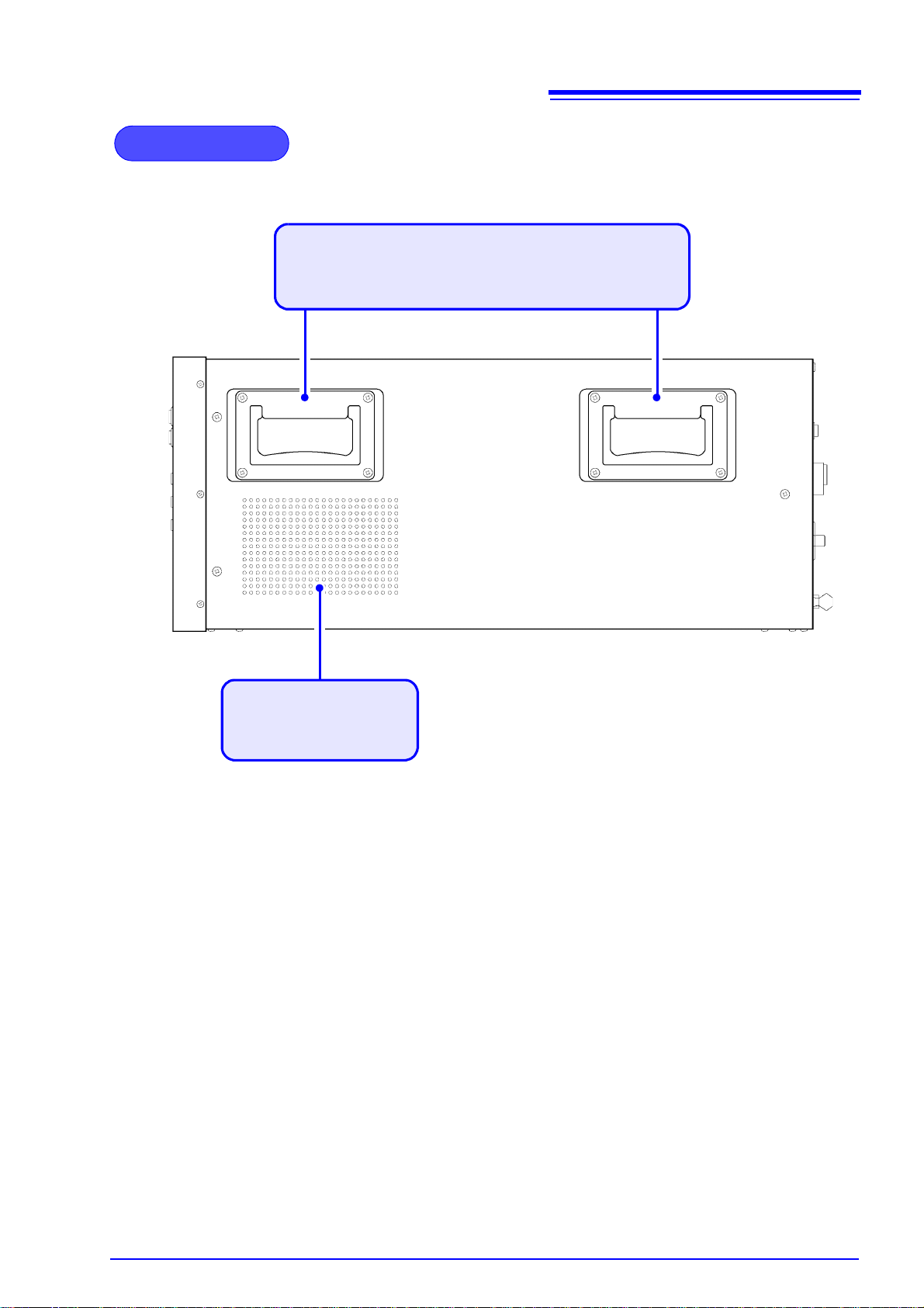
Side Panel
Handle
It should be moved by at least two p eople, who shoul d grip it using
the handles on the left and right sides.
Vent
Keep clear of obstructions.
1.2 Names and Functions of Parts

10
VA (+) IR:1000.0
VB (+) IR: 250.0
TERMINAL:
OUT1:11100000
OUT2:11100000
OUT3:11100000
OUT4:11100000 VMA:1000.0 OK
VMB: 250.0 OK
■ Screen P1 : Displays output voltage settings.
■ Screen P2: Alarm/GP-IB address setting display
Output voltage setting
VA: Displays the power supply A circuit voltage setting.
VB: Displays the power supply B circuit voltage setting.
Temperature error display
When a temperature error is d ete cte d,
"TEMP" flashes in reverse video.
Terminal output setting state
The setting is 0 or 1.
From left to right, OUTn row 1 → row 8
0: High-impedance
1: ON
Monitor voltage value
VMA: Displays the voltage
monitor value for the
power supply A circuit.
VMB: Displays the voltage
monitor value for the
power supply B circuit.
*Fixed-po int, zero-suppr essed.
Voltage error alarm results
VA ALARM: 19
VB ALARM: 19
GPIB ADDR: 1
Voltage error alarm setting
VA: Power supply A circ uit voltage error alar m setting ± (% )
VB: Power supply B circ uit voltage error alar m setting ± (% )
OK: The monitor voltage error
relative to the output voltage setting falls with in the
normal range relative to
the voltage error alarm
setting.
NG: The monitor voltage error
relative to the output voltage setting indicates an
error relative to the voltage
error alarm setting.
Temperature error display
When a temperature error is
detected, "TEMP" flashes in reverse video.
GP-IB address
L
Key lock display
When the keys are
locked, flashes
in reverse video.
L
TEMP
TEMP
L
TEMP
TEMP
1.3 Screen Layout
1.3 Screen Layout
The LCD screen cons ists of two dis play pa ges. W hen th e SM78 60 i s turne d on,
page 1 is shown.
The scroll keys on th e front of the device (PA GE UP ▲/ PAG E D OW N▼) are
used to scroll among the di splay pages, which can also be selected directly by
sending the “
See: Message List "PAG" (p.30)
PAG” command from the GP-IB or RS-232C interface.

11
8
Install this device (p.3)
1
Rear PanelFront Panel
Turn the power on (p.15)
6
Connect the external interface
4
• Using the GP-IB or RS-232C interface
(p.17)
• Using the EXT I/O (p.33)
Connect the power cord (p.12)
2
Make device settings (p.16)
(via the external interface)
7
Connect the device to the measuring instrument. (p.13)
3
Be sure to complete the pre-operation inspection (p.14) before
using the device
5
Activate the power source
2
4
6
3
2.1 Installation & Connection Procedures
Preparing to Use the Device
and Supplying
Power Chapter 2
2.1 Installation & Connection Procedures
Be sure to read the "Operating Precautions" (p.3) befo re installing and connecting
this device.
12
Rear Panel
1 Confirm that the device is turned off.
2 Confirm that the mains supply voltage
matches the device, and connect the
power cord to the power inlet on the
device.
3 Plug the power cord into the mains outlet.
Power inlet
2.2 Connecting the Power Cord
2.2 Connecting the Power Cord
• Before turning the device on, make sure the supply voltage matches that
indicated on its power connector . Connection to an improper supply voltage may damage the device and present an electrical hazard.
• To avoid electrical accidents and to maintain the safety specific at ion s of
this device, connect the power cord only to a 3-contact (two-conductor +
ground) outlet.
• Before using the device, make sure that the insulation on the power cord
is undamaged and that no bare conductors are improperly exposed.
Using the device in such conditions could cause an electric shock, so
contact your dealer or Hioki representative for replacements.
To avoid damaging the po wer cord, grasp the plug, not the cord, wh en unplugging it from the power outlet.
Turn off the power before disconnecting the power cord.
Connection Methods

2.3 Connecting the Device to the Measuring Instrument
Rear Panel
1 Confirm that the device is turned off.
2 Connect the included voltage output con-
nector to the voltage output terminal on
the rear of the device.
Voltage output terminal
6 5 47
3
2
10
8
9
1
Voltage output pin assignments
(View of terminal on device)
*1 On the SM7860-05, -06, -2 5, an d - 26, ser v es as t he di s ch argin g
terminal.
*2 On the SM7860-05, -06, -07, -25, -26 and -27, serves as the dis-
charging terminal.
Pin No. OUT1
Circuit A
OUT2
*1
Circuit A
OUT3
Circuit B
OUT4
*2
Circuit B
1 CH1 CH1 CH1 CH1
2 CH2 CH2 CH2 CH2
3 CH3 CH3 CH3 CH3
4 CH4 CH4 CH4 CH4
5 CH5 CH5 CH5 CH5
6 CH6 CH6 CH6 CH6
7 CH7 CH7 CH7 CH7
8 CH8 CH8 CH8 CH8
9 NC NC NC NC
10 COM COM COM COM
2.3 Connecting the Device t o the Measuring
Instrument
To avoid electric shock or damage to the equ ipment, always observe the
following precautions when connecting to voltage output terminal.
• Always turn off the power to the device and to any dev ices to be con-
nected before connecting the voltage output connectors.
To avoid damaging the device, be sure to observe the following precautions:
• Do not connect the device to a load with a charge in exc ess of the output v oltage range.
• Do not connect the device to a load with a charge that has the opposite polarity
of the output voltage range.
• Do not connect the device to a load that has a charge when the device's power
supply is turned off.
13
Connection Methods
Specifications

14
Do not use a damaged cor d because
doing so may result in electric
shock. (Replace the cord with a new
one.)
Metal Exposed
• Is the power cord insulation torn, or is
any metal exposed?
• Is the connection cord insulation torn, or
is any metal exposed?
1
No Metal Exposed
Before using the device the fir st time, verify that it operates nor mally to ensure that the no
damage occurred during storage or shipping. If you find any damage, contact your dealer or
Hioki representative.
Peripheral Device Inspection
If damage is evident, request repairs.
Yes
Is damage to the device evident?
Device Inspecti on
2
No
Inspection complete
Please read the "Operating Precautions" (p.3) before use.
Use of a supply voltage outside the
specified range may damage the device or cause electric shock.
No
Does the supply voltage of your power
source match the supply voltage indicated
above the power source inlet on the rear of
the device?
Yes
2.4 Pre-Operation Inspection
2.4 Pre-Operation Inspection
2.5 Turning the Power On and Off
Rear Panel
POWER switch
Turn the POWER switch on ( ).
The power indicator and LCD screen on the front of the device will light up.
Before Starting Measurement
To obtain precise measurements, provide about an hour warm-up after turning power on.
Turn the POWER switch off ( ).
2.5 Turning the Power On and Off
• Before turning the device on, make sure the supply voltage matches that
indicated on its power connector. Connection to an improper supply voltage may damage the device and present an electrical hazard.
• When turning the device on and off, do not touch the voltage output terminals. Doing so may cause electric shock.
When turning the device on and off, do not connect a load to the voltag e output
terminals. Tur ning the device o n or off with a l oad connected may damage the
load.
15
Turning Power On
Turning Power Off

16
2.6 Setting the Operating Conditions
2.6 Setting the Operating Conditions
This section describes how to set the operating conditions according to the manner in which the device is to be used.
Settings are configured via either of the device’s external interfaces:
See: GP-IB/RS-232C Interface (p.17)
The device cannot be configured directly in a standalone manner.
Setting function Description of operation and settings See page
Output voltage
Voltage error alarm
LCD display mode
Sets the output volta ge.
Setup ranges: 1.0 to 1000.0 V (0.1 V resolution)
Generates an alarm when the monitor voltage error relative to the output
voltage setting falls outside the set value range.
Setup ranges: ±2 to ±19% (1% resolution)
Turns the LCD dis play on and off.
[OFF/ ON]
p.29
p.29
p.30

17
Wiring Diagram ( p.19)
Connect the device and Controller with a GP-IB or RS-232C
Interface Cable
Communications Protocol Settings
Enter a GP-IB address.
Set the device to the same
communications protocol as
the controller
Set the transmission format.
3.1 Overview and Features
Communication
(GP-IB/RS-232C Interface) Chapter 3
The symbol shown below in dicates that the following ins tructions are sp ecific to
the RS-232C or the GP -IB interface. Instructio ns without these symbo ls are for
both the RS-232C and the GP-IB interface.
: GP-IB only
: RS-232C only
Before Use • Always make use of the connector screws to affix the GP-IB or RS-232C con-
nectors.
• When issuing commands tha t contain data, make certain tha t the data is pro-
vided in the specified format.
3.1 Overview and Features
The device provides standard communication fun ctionality in the form of GP-IB
and RS-232C interfaces, both of which can be used to control the device
remotely and to transfer data.
• This device is designed with reference to the following standard:
Reference standard IEEE 488.1-1987

18
3.2 Specifications
3.2 Specifications
Precautions
RS-232C and GP-IB communications cannot be used simultaneously.
GP-IB Specifica-
tions
Electrical machinery specifications: IEEE std. 488.1-1987 compliant
Address setting : Can be set to talker/listener addresses 1 to 30.
Interface Functions
SH1 All Source Handshake functions ●
AH1 All Acceptor Handshake functions ●
T6 Basic talker functions
Serial poll function
Talk-only mode
The talker cancel function with MLA (My Listen Address)
L4 Basic listener functions
Listen-only mode
The listener cancel function with MTA (My Talk Address)
SR1 All Service Request functions ●
RL1 All Remote/Local functions ●
PP0 Parallel Poll function −
DC1 All Device Clear functions ●
DT1 All Device Trigger functions ●
C0 Controller functions −
E2 Tri-state output
Operating Code: ASCII codes
●
●
−
●
●
−
●
RS-232C Specifica-
tions
Transfer method Communications: Full duplex
Synchron ization: Start-stop synchronization
Baud rate 38400 bps
Data length 8 bits
Parity none
Stop bit 1 bit
Flow control none
Electrical specification Input voltage levels 5 to 15 V : ON
-15 to -5 V : OFF
Output voltage levels +5 V or more : ON
-5 V or less : OFF
Connector RS-232C Interface Connector Pinout
(Male 9-pin D-sub, with #4-40 attachment screws)
The I/O connector is a DTE (Data Terminal Equipment)
configuration
Recommended cables:
• Model 9637 RS-232C Cable
• Model 9638 RS-232C Cable
See: "3.3 Connect a cable to the GP-IB connector or
RS-232C connector" (p.19)
Operating Code: ASCII codes
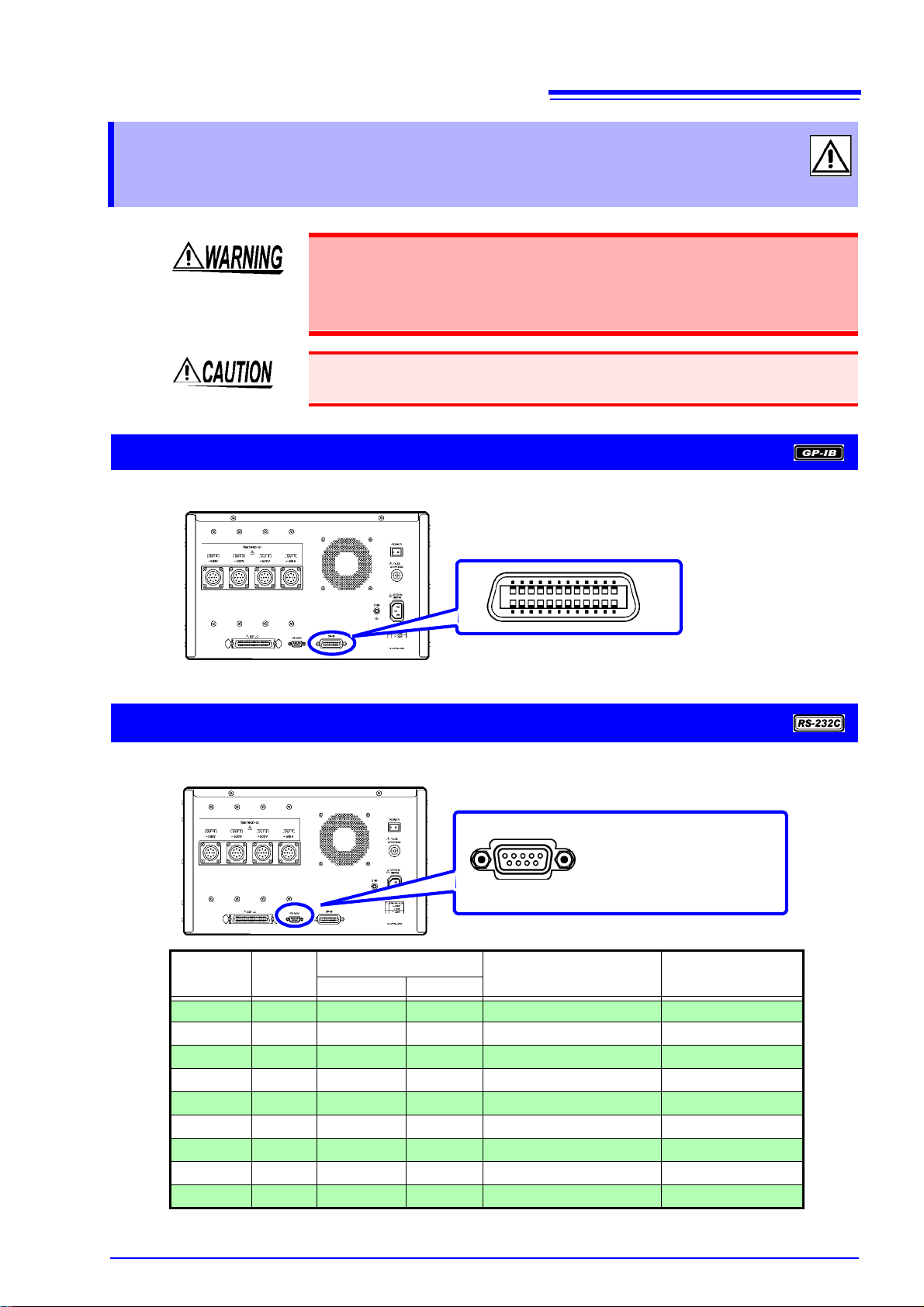
3.3 Connect a cable to the GP-IB connector or RS-232C connector
Rear Panel
Recommended cable:
HIOKI Model 9151-02 GP-IB Connector Cable (2 m)
6 7 8 9
1 2 3 4 5
Rear Panel
Male 9-pin D-sub
#4-40 attaching screws
3.3 Connect a cable to the GP-IB
connector or RS-232C connector
• Always turn both devices OFF when connecting and disconnecting an
interface connector. Otherwise, an electric shock accident may occur.
• Failure to fasten the connect ors properly may re sult is sub-spe cification
performance or damage to the equipment.
To avoid damage to the device, do not short-circuit the terminal and do not input
voltage to the terminal.
Using the GP-IB Interface
Connect the GP-IB cable to the GP-IB connector.
19
Using the RS-232C Interface
Connect the RS-232C cable to the RS-232C connector.
Pin No.
1 DCD CF CD
2 RXD BB RD
3 TXD BA SD
4DTRCD ER
5 GND AB SG
6DSRCC DR
7 RTS CA RS
8 CTS CB CS
9 RI CE CI
Signal
Name
Code Addr.
EIA JIS
Mutual connection
circuit name
Carrier Detect Not used
Receive Data
Transm it Data
Data Terminal Ready Not used
Signal Ground
Data Set Ready Not used
Request to Send Not used
Clear to Send Not used
Ring Indicator Not used
Remarks

20
Recommended cable:
HIOKI
Model 9637 RS-232C
Cable (1.8 m)
Crossover Wiring
Female 9-pin
D-sub
Model SM7860
end
Female 9-pin
D-sub
PC/AT-end
Pin No. Pin No.
DCD 1 1 DCD
RxD 2 2 RxD
TxD 3 3 TxD
DTR 4 4 DTR
GND 5 5 GND
DSR 6 6 DSR
RTS 7 7 RTS
CTS 8 8 CTS
RI 9 9 RI
3.3 Connect a cable to the GP-IB connector or RS-232C connector
When connecting the device to a computer
Use a crossover cable with female 9-pin D-sub connectors.

3.4 Configuring the Communications Protocol
1 Press and hold the scroll keys (PAG E U P▲/PA GE D O WN ▼) on the front of the device
for about 7 seconds. (The address can be set from the P1 or P2 screen.)
■ Screen P1: Status display
3 When finished making the setting, turn off the device.
4 Turn on the device.
The device will revert to the initial screen, and the GP-IB address will be set to the
selected address.
GPIB ADDR: 1
VA (+) IR:1000.0
VB (+) IR: 250.0
TERMINAL:
OUT1:11100000
OUT2:11100000
OUT3:11100000
OUT4:11100000 VMA:1000.0 OK
VMB: 250.0 OK
2 Using the scroll keys (PAGE UP▲/PAGE DOWN▼), set the desired address.
(Valid setting range: 1 to 30)
3.4 Configuring the Communications Protocol
Configuring GP-IB Interface Communications
Setting the address
21
Configuring RS-232C Interface Communications
Communication conditions
Baud rate 38400 bps
Parity none
Stop bit 1 bit
Data 8 bits
Flow control none
Remote switching requests
Send the “RMT” command from the RS-232C interface.
RS-232C interface communications will not be available until the “RMT” com-
mand is sent.
22
Program Messages
Response Messages
SM7860
Program Messages
Messages
Command Message
Query Message
Response Message
Controller
Message types are further categorized as follows
When issuing commands that contain data, make certain that the data is provided in the specified format.
3.5 Communication Methods
3.5 Communication Methods
Various messages are supported for controlling the device through the interfaces.
Messages can be either program messages, sent from the controller such as PC to the
device, or response messages, sent from the device to the controller.
Program Messages
1. Command Messages and Query Messages
(1) Command Messages
Commands that control the device, for example to configure settings or reset the
device.
(2) Query Messages
Requests for respon ses relating to result s of operation or me asurement, or the
state of device settings.
Query commands end with a question (
2. Message delimiter (terminator)
This device recognizes the following input message delimiters:
CR+LR with EOI
LF with EOI
CR with EOI
EOI
CR+LF
LF
?) mark.
Response Messages
1. Response Messages
When a query messag e is recei ved, its s yntax is c hecked and a r espons e message is generated.
2. Message delimiter (terminator)
The following three response message delimiters can be specified with the
“
DLM” command:
LF (initial setting)
CR+LF
EOI
Separators
1. Message Unit Separator
Multiple messag e can be writte n in on e line by se parati ng them wi th semicol ons
“
; ”
2. Header Separator
In a message consisting of both a header and data, the header is separated from
the data by a space “ ” (ASCII code 20H).
3. Data Separator
In a message containing mu ltiple data items, commas are required to separate
the data items from one another.
Data Formats
Query messages use the formats outlined in Table 1. The format is selected
according to the command.
23
3.5 Communication Methods
Table 1: Response Messages and Parameter Data Types
Data
type
NR1 Integer 0, 1, 2, 3, etc. Parameter settings, etc.
NR2
NR3
ASCII ASCII string XXXXXXXXXXXXXXXX Primarily hardware IDs
Description Example Notes
Fixed-point decimal number
Floating-point decimal number
+12.345, 400.0, etc. Primarily settings
+1.234±50, etc.
Primarily settings and measured values

24
bit 7bit 6bit 5bit 4bit 3bit 2bit 1bit 0
ERR
RQS
ESB MAV DSB
unused unused
unused
MSS
& &&&&&&
bit 7bit 6bit 5bit 4bit 3bit 2bit 1bit 0
ERR x ESB MAV DSB
unused unused
unused
Logical
sum
Status Byte
Register (STB)
Service Request Enable
Register (SRER)
Service Request
occurrence
Output Queue data information
Stand ard Event Register Information
Each of these bits corresponds to a specific event register
Overview of Service Request Occurrence
3.5 Communication Methods
Status Byte Register
RS-232C reads the status bytes to find out the status of the device.
The device adopts th e IE E E48 8.1 -1987 def ined status model for parts related to
the serial polling performed by the service request function. A trigger for
generating a service request is called an event.
The Status Byte Register contains information about the event registers and the
output queue. Required items are selected from this information by masking with
the Service Request Enable Register. When any bit selected by the mask is set,
bit 6 (MSS; the Master Summary Status) of the Status Byte Register is also set,
which generates an SRQ (Service Request) message and dispatches a service
request.
For RS-232C, bit 4 (MAV message available) of the status byte register is not
set.
25
3.5 Communication Methods
Status Byte Register (STB)_______________________________________
A status byte register is an 8-bit register output from the unit to the controller
during serial polling. If even one of the status byte register bits enabled by the
service request enable register changes from "0" to "1" the MSS bit becomes 1.
At the same time, the RQS bit also becomes "1" and a service request is
generated.
The RQS bit is always synchronized with the service request and only read and
simultaneously cleared upon being serial polled. The MSS bit is only read by an
"
*STB?" query and is not cleared until the event is cleared by a command such
as a "
*CLS" command.
Bit 7 ERR
Bit 6 RQS
MSS
Bit 5 ESB
Bit 4 MAV
Bit 3 DSB
Bit 2 −
Bit 1 −
Bit 0 −
Unrecoverable error
Set to 1 when a service request is dispatched.
This is the logical sum of the other bits of the Status Byte Regis-
ter.
Standard Event Status (logical sum) bit
This is logical sum of the St andard Event Status Register.
Message available
Indicates that a message is present in the output queue.
Event Status (logical sum) bit
This is the logical sum of Event Status Register.
unused
unused
unused
Service Request Enable Register (SRER)___________________________
This register masks the Status Byte Register. Setting a bit of this register to 1
enables the corresponding bit of the Status Byte Register to be used.

26
3.5 Communication Methods
Event Registers
Standard Event Status Register (SESR)____________________________
A standard event status register is an 8-bit register.
If any bit in the Standard Event Status Register is set to 1 (after masking by the
Standard Event Status Enable Register), bit 5 (ESB) of the Status Byte Register
is set to 1.
See: "Standard Event Status Enable Register (SESER)" (p.27)
The standard event status register is cleared at the following times:
• When a "
• When a "
• When the device is powered on
*CLS" command is executed
ERR?" command is executed
Bit 7 PON
Bit 6 URQ
Bit 5 CME
Bit 4 EXE
Bit 3 DDE
Bit 2 QYE
Bit 1 RQC
Bit 0 OPC
Power-On Flag
Set to 1 when the power is turned on, or upon recovery from an outage.
User Request
unused
Command error (The command to the message terminator is ignored.)
This bit is set to 1 when a recei ved command contains a sy ntactic or sema ntic
error:
• Program header error
• Incorrect number of data parameters
• Invalid parameter format
• Received a command not supported by the device
Execution Error
This bit is set to 1 when a received command cannot be executed for some
reason.
• The specified data value is outside of the set range
• The specified setting data cannot be set
• Execution is prevented by some other operation being performed
Device-Dependent Error
This bit is set to 1 when a comm and ca nnot be ex ecute d due to some reason
other than a command error, a query error or an execution error.
• When the command cannot be executed because there is an internal
anomaly
Query Error (the output queue is cleared)
This bit is set to 1 when a q uery erro r is detected by the co ntroller of th e output
queue.
• When an attempt has been made to read an empty output queue (GP-IB
only)
• When the data overflows the output queue
• When data in the output queue has been lost
Request Control
unused
Operation Complete
This bit is set to 1 in response to an "
• It indicates the com pletio n of operati ons of all mess ages up to th e "*OPC"
command
*OPC" command.
27
bit 7bit 6bit 5bit 4bit 3bit 2bit 1bit 0
PON URQ CME EXE DDE QYE RQC OPC
&&&&&&&&
bit 7bit 6bit 5bit 4bit 3bit 2bit 1bit 0
PON URQ CME EXE DDE QYE RQC OPC
Standard Event Status Register (SESR)
Standard Event Status Enable Register (SESER)
bit 6bit 5bit 4
SRQ
MSS
ESB MAV
Logical
sum
3.5 Communication Methods
Standar d Event Status Enable Register (SESER) ____________________
Setting any bit of the Standard Event Status Enable Register to 1 enables access
to the corresponding bit of the Standard Event Status Register.
Standard Event Status Register (SESR) and Standard Event Status Enable
Register (SESER)

28
bit 7bit 6bit 5bit 4bit 3bit 2bit 1bit 0
− MLE
HDE DFE DRE CNE ISE BDE
Error Register
PON URQ CME EXE DDE QYE RQC OPC
Standard Event Status Register
bit 7bit 6bit 5bit 4bit 3bit 2bit 1bit 0
MLE: Message Length Error HDE: Header Error
DFE: Data Format Error DRE: Data Range Error
CNE: Can Not Execute ISE: Internal communication Error
BDE: Environment Backup was Damaged (RAM)
Error Register structure
3.5 Communication Methods
Error Registers
The Error Register, which consists of 8 bits, manages error information. The
contents of this register are aggregated in the CME, EXE, DDE, and QYE bits of
the Standard Event Status Register (no mask processing is performed).
Error register-related message are listed below.
*CLS
Clears the following registers:
• Status Byte Register
• Standard Event Status Register
• Error Register
ERR?
Queries and clears the Error Register.
Bit No. Name Event/status indicated by set bit
Bit 7 −
Bit 6
Bit 5
Bit 4
Bit 3
Bit 2
Bit 1
Bit 0
MLE
HDE
DFE
DRE
CNE
ISE
BDE
Unused
Message Length Error
Set when the message length exceeds the allowable range.
The bit is reset after the register is read.
Message Header Error
Set when an unrecognizable message header is received.
The bit is reset after the register is read.
Data Format Error
Set when the number of parameters exceeds the stipulated number or
when there is an unrecognizable parameter.
The bit is reset after the register is read.
Data Range Error
Set when a parameter falls outside the stipulated range.
The bit is reset after the register is read.
Unexecutable command
Set when an unexecutable command is received.
The bit is reset after the register is read.
Internal communication Error
Set when an internal communication error occurs.
The bit is reset after the register is read.
Environment Backup was Damaged
Set when data stored in the instrument's backup RAM is corrupted.
The bit is reset after the register is read.

3.6 Message List
Model Lower limit (V) Uppe r limit (V)
SM7860-01, -21 1.0 500.0
SM7860-02, -22 250.0 1000.0
SM7860-03, -23 1.0 500.0
SM7860-04, -24 250.0 1000.0
SM7860-05, -25 1.0 500.0
SM7860-06, -26 250.0 1000.0
SM7860-07, -27 1.0 10.0
3.6 Message List
RS-232C-only commands are indicated by .
When using the RS -232C interface to send com mands, include a unifor m wait
time of 100 ms (excluding the following exceptions).
Command Description Formats
Communication conditions
RMT
Remote switching request
Delimiter
DLM
DLM?
Talker delimiter specification
d1 (delimiter specification: 0 to 2)
0: LF<EOI> Default
1: CRLF<EOI>
2: <EOI>
Note: This setting reverts to it s defa ul t v alu e when th e instrument
Delimiter query
The contents of responses are the same as the settings.
Output voltage setting
VAI
VAI?
VBI
VBI?
Circuit A output voltage setting
d1: 1.0 to 1000.0 V
Note: Set as an absolute value.
Circuit A output voltage setting query
The contents of responses are the same as the settings.
Circuit B output voltage setting
d1: 1.0 to 1000.0 V
Note: Set as an absolute value.
Circuit B output voltage setting query
The contents of responses are the same as the settings.
Output voltage sett ing range by mo del
is powered on. A combination CR+LF is used as the RS232C delimiter for both data transmission and reception.
The valid setting range varies with the model.
The valid setting range varies with the model.
[Format] RMT
[Format] DLM d1
[Format] DLM?
[Response] d1
[Format] VAI d1
[Format] VAI?
[Response] d1
[Format] VBI d1
[Format] VBI?
[Response] d1
29
d1: NR1 format
d1: NR2 format
d1: NR2 format
Alarm setting
ARM
ARM?
Voltage error alarm setting
d1: 2 to 19%, Circuit A voltage error alarm setting
d2: 2 to 19%, Circuit B voltage error alarm setting
Note: d1 or d2 can be omitted.
Volt age error alarm setting query
The contents of responses are the same as the settings.
[Format] ARM d1,d2
ARM d1
ARM ,d2
[Format] ARM?
[Response] d1,d2

30
3.6 Message List
Command Description Formats
Voltage monitor
VMA?
VMB?
LCD display mode
LCD
LCD?
PAG
Error information
ERR?
Others
*RST
*IDN?
*SAV
*RCL
*CLS
*SRE
*SRE?
Circuit A power supply voltage monitor value query [Format] VMA?
[Response] d1: NR2 format
Circuit B power supply voltage monitor value query [Format] VMB?
[Response] d1: NR2 format
LCD display mode setting
d1 (Display mode: 0 to 1)
0: OFF (Display off)
1: ON (Display on)
LCD display mode query
The contents of responses are the same as the settings.
LCD display page specification
d1 (Page number: 0 to 1)
0: Output voltage setting, monitor voltage value, channel-spe-
cific output setting state
1: Alarm setting, GP-IB address
Error information query
d1 (Error information: 0 to 127)
Note: Error information is cleared when the response is output.
Device initialization
Initializes all settings to their factory values.
Device operation will be stopped.
Hardware ID query
Returns the device’s hard ware ID as the respo ns e.
d1 (HIOKI, SM7860-XX, 0, 01.00)
Note: The SM7860-2X is shown as "SM7860-0X."
Save environmental data
(output voltage setting and alarm setting)
d1 (Environmental data no.: 0 to 3)
Recall environmental data
(output voltage setting and alarm setting)
d1 (Environmental data no.: 0 to 3)
Clear status register
Sets the service request enable register.
d1 (0 to 255)
Service request enable register query
d1 (0 to 63, 128 to 191)
[Format] LCD d1
[Format] LCD?
[Response] d1: NR1 format
[Format] PAG d1
[Format] ERR?
[Response] d1: NR1 format
[Format] *RST
[Format] *IDN?
[Response] d1: String
[Format] *SAV d1
[Format] *RCL d1
[Format] *CLS
[Format] *SRE d1
[Format] *SRE?
[Response] d1: NR1 format
d1: NR1 format
d1: NR1 format
d1: NR1 format
d1: NR1 format
d1: NR1 format
*STB?
*ESE
*ESE?
*ESR?
Note: Bit 6 is not set by
Status byte register query
d1 (0 to 255)
Sets the standard event status enable register.
d1 (0 to 255)
Standard event status enable register query
The contents of responses are the same as the settings.
Standard event status register query
d1 (0 to 255)
*SRE.
[Format] *STB?
[Response] d1: NR1 format
[Format] *ESE d1
d1: NR1 format
[Format] *ESE?
[Response] d1: NR1 format
[Format] *ESR?
[Response] d1: NR1 format

3.6 Message List
Command Description Formats
*OPC
*OPC?
CNF
CNF?
KLC
KLC?
Sets the standard event status register’s OPC bit after all ongoing
operations have completed.
This command is used to detect the compl etion of comman ds that
involve time-consuming processing.
Returns the value 1 when all ongoing operations have completed.
d1: 1
Operating environment se ttin g
d1 (Interlock control enable/disable: 0 to 1)
0: CONNECT (Enables interlock.)
1: CUTOFF (Disables interlock.) Default
Operating environment que ry
The contents of responses are the same as the settings.
Key lock setting
d1 (0 to 1)
0: Key lock off
1: Key lock on
Key lock query
d1 (0 to 1)
The contents of responses are the same as the settings.
[Format] *OPC
[Format] *OPC?
[Response] d1: NR1 format
[Format] CNF d1
[Format] CNF?
[Response] d1
[Format] KLC d1
[Format] KLC?
[Response] d1: NR1 format
31
d1: NR1 format
d1: NR1 format

32
3.7 Listener Specification Precautions
3.7 Listener Specification Precautions
Input buffer size
Multiple command messages can be transferred at once by joining them with
message separators. Since the instrument provides an 128-byte input buffer, the
instrument is unabl e to receive message str ings in excess of 127 cha racters in
length. In this case, the entire command will be ignored (discarded), and the
Error Register's MLE (Message Length Error) bit will be set.
Reading from the output buffer
The output buffer us es a FIFO design, with old er data being read first. Consequently, the read value may diffe r from the expe cte d va lue under ce rta in circ umstances, for example if no response is acquired after issuing a query.
Additionally, the o utpu t b uffe r is 511 b yte s i n s i ze. If d ata in excess of 511 by tes
is written to the buffer , it will be di scarded, and the Error Registe r's QY E (Que ry
Error) bit will be set.
33
Connect the device’s EXT I/O
connector to the signal output
or input device.
Rear Panel
4.1 External Input/Output Connector and Signals
External Control Chapter 4
This chapter describes how to use the EXT I/O connector on the rear of the
device to control the device.
4.1 External Input/Output Connector and
Signals
To avoid electric shock or damage to the equ ipment, always observe the
following precautions when connecting to the EXT I/O connector.
• Always turn off the power to the device and to any dev ices to be con-
nected before making connections.
• During operation, a wire becoming dislocated and contacting another
conductive object can be serious hazard. Ensure that the cable is
securely attached to the EXT I/O connector.
• Ensure that devices and systems to be connected to the EXT I/O connec-
tor are properly isolated.
To avoid damage to the device, observe the following cautions:
• Do not apply voltage or current to the EXT I/O connector that exceeds their ratings.
• When driving relay s, be sure to ins tall diodes to abso rb counter-elec tromotive
force.
See: "Connector Type and Signal Pinouts" (p.34)
34
EXT I/O connector
Connector
• 57RE-40500-730B (50-pin: DDK)
Rear Panel
252423222120191817161514
1312111098765432
1
50494847464544434241403938373635343332313029282726
4.1 External Input/Output Connector and Signals
Connector Type and Signal Pinouts
Pin Signal name I/O Pin Signal name I/O
1 COM - 26 COM 2 EXT_DCV2(+24V)
3 OUTPUT
4 OUT1(1)_ON
5 OUT1(3)_ON
6 OUT1(5)_ON
7 OUT1(7)_ON
8 OUT2(1)_ON
9 OUT2(3)_ON
10 OUT2(5)_ON
11 OUT2(7)_ON
12 OUT3(1)_ON
13 OUT3(3)_ON
14 OUT3(5)_ON
15 OUT3(7)_ON
16 OUT4(1)_ON
17 OUT4(3)_ON
18 OUT4(5)_ON
19 OUT4(7)_ON
20
21
22
23
(Reserved)
(Reserved)
(Reserved)
(Reserved)
24 ALARM
25 TEMP
Input
Input
Input
Input
Input
Input
Input
Input
Input
Input
Input
Input
Input
Input
Input
Input
Input
Input
Output
Output
27 EXT_DCV2(+24V)
28 INTERLOCK
29 OUT1(2)_ON
30 OUT1(4)_ON
31 OUT1(6)_ON
32 OUT1(8)_ON
33 OUT2(2)_ON
34 OUT2(4)_ON
35 OUT2(6)_ON
36 OUT2(8)_ON
37 OUT3(2)_ON
38 OUT3(4)_ON
39 OUT3(6)_ON
40 OUT3(8)_ON
41 OUT4(2)_ON
42 OUT4(4)_ON
43 OUT4(6)_ON
44 OUT4(8)_ON
45
46
47
48
(Reserved)
(Reserved)
(Reserved)
(Reserved)
49 BUSY
50
(Reserved)
Output
Input
Input
Input
Input
Input
Input
Input
Input
Input
Input
Input
Input
Input
Input
Input
Input
Input
Input
Do not connect to reserved pins.

4.1 External Input/Output Connector and Signals
Signal Descriptions
Input Signals
EXT_DCV2(+24V) External power source input
OUTPUT Output on/off setting
OUT 1(1)_ON to OUT 1(8)_ON Channel-specific on/off settin g
OUT 2(1)_ON to OUT 2(8)_ON Channel-specific on/off settin g
OUT 3(1)_ON to OUT 3(8)_ON Channel-specific on/off settin g
OUT 4(1)_ON to OUT 4(8)_ON Channel-specific on/off settin g
INTERLOCK When on, no volt ag e can be generated.
•The INTERLOCK signal cannot be used unl ess it has been enabled with the
operating environ ment s etting (CNF =0). The devi ce s hips with this settin g disabled (CNF=1).
See: Message List "CNF" (p.31)
35
• The output voltage cannot be changed while the OUTPUT
Output Signals
ALARM Generated voltage alarm
BUSY Voltage being output
TEMP Temperature alarm
signal is enabled.

36
OUTPUT
BUSY
t1
Pre v ious ALARM r es u lt
ALARM
OUT1 (CH1) to (CH8)
OUT2 (CH1) to (CH8)
OUT3 (CH1) to (CH8)
Volt age out put * 1
New ALARM resu lt
t2
t5
t6
t4
t9
t3 t7
t8
t11t10
High-impedance
Discharge
OUT2 (CH1) to (CH8)
OUT4 (CH1) to (CH8)
Discharge*3
OUT1(1)_ON to (8)_ON
OUT2(1)_ON to (8)_ON
OUT3(1)_ON to (8)_ON
OUT4(1)_ON to (8)_ON
OUT3 (CH1) to (CH8)
OUT4 (CH1) to (CH8)
Volt age out pu t *2
High-impedance
High-impedance
High-impedance
High-impedance
High-impedance
External output terminal
Voltage output terminal
*1 to *3 vary with the model.
*1: SM7860-01, -02, -21, 22 : OUT1
SM7860-03, 04, 05, 06, -23, 24, 25, 26 : OUT1 to OUT2
SM7860-07, -27 : OUT1 to OUT3
*2: SM7860-01, 02, 05, 06, -21, 22, 25, 26 : OUT3
SM7860-03, 04, -23, 24 : OUT3 to OUT4
*3: SM7860-05, 06, -25, 26 : OUT2, OUT4
SM7860-07, -27 : OUT4
4.2 Timing Chart
4.2 Timing Chart
Each signal level indicates a corresponding voltage level.

Timing Chart Interval Descriptions
Interval Description Duration
Channel setup time 100 μs or more
t1
Channel hold time 200 μs or more
t2
t3
t4
t5
t6
t7
t8
t9
t10
t11
OUTPUT ON → Busy delay time
OUTPUT ON → Voltage output delay time
Alarm delay time 3.5 ms or less
Output pulse width 8 ms or more
OUTPUT OFF → Busy delay time
OUTPUT OFF → Voltage output delay time
Output off time 4 ms or more
OUTPUT ON → Discharging start delay time
OUTPUT OFF → Discharging complete delay time
200 μs or less
600
μs or less
800 μs or less
2.5 ms or less
1.2 ms or less
1.1 ms or less
37
4.2 Timing Chart
38
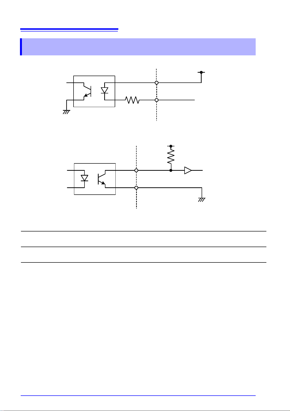
Input Circuit
Output Circuit
SM7860 side
External device side
EXT_DC2
Input signals
24 VDC
SM7860 side
External device side
COM
5 to 24 VDC
Output signals
4.3 Internal Circuitry
4.3 Internal Circuitry
Input Signals
Output Signals
Input method Photocoupler-isolated input
Input voltage LOW: 0 to 0.5 V, HIGH: 24 V±10%
Output method Photocoupler -open collector output
Output voltage/ current LOW < 0.5 V, HIGH > 5 to 24 V (depends on external voltage)/ Max. 5 mA

5.1 General Specifications
Specifications Chapter 5
5.1 General Specifications
Operating environment Indoors, Pollution degree 2, up to 2,000 m (6562-ft.) ASL
39
Operating temperature and
humidity
Storage temperature and
humidity
Dielectric strength 1.62 kV AC for 60 s, Cutoff cu rren t 10 m A, be tween all pow e r term ina ls and prot ect iv e
Applicable Standards
Safety
Power source Rated supply voltage
Maximum rated power 860 VA
Dimensions Approx. 425W × 249H × 581D mm (16.73"W × 9.80"H × 22.87"D)
Mass Approx. 45 kg (1587.3 oz.) (SM7860-01, 02, 03, 04, 05, 06, 21, 22, 23, 24, 25, 26)
Accessories Power Cord......................................... ...... ..... ...... ...... ..... ...... ..1
0 to 40°C (32 to 104°F), 80%RH or less (non-condensing)
-10 to 55°C (14 to 131°F), 80%RH or less (non-condensing)
ground, interfaces, a nd measurem ent termin als, b etween p ower supply line and power
supply neutral
EN61010
SM7860-01, 02, 03, 04, 05, 06, 07: 100 VAC, 110 VAC (Must specify when ordering)
SM7860-21, 22, 23, 24, 25, 26, 27: 220 VAC
(Voltage fluctuations of
Rated supply frequency : 50/60 Hz
Anticipated transient overvoltage : 2,500 V
Approx. 32 kg (1128.7 oz.) (SM7860-07, 27)
Instruction manual..................................................................1
Voltage output connector
SM7860-01, -02, -21, -22....................................................2
SM7860-03, -04, -05, -06, -07, -23, -24, -25, -26, -27.........4
±10% from the rated supply voltage are taken into account)
Options Model 9637 RS-232C Cable (9pin-9pin/Cross/1.8m)
Model 9638 RS-232C Cable (9pin-25pin/Cross/1.8m)
Model 9151-02 GP-IB Connector Cable (2 m)
Replacement part Fuse: MF60NRF-8A (250V M 8.0A φ6.4×30 mm)

40
5.2 Basic Specifications
5.2 Basic Specificat io n s
Design
Model Circuit A Circuit B
Maximum outp ut current 430 mA (200 VA) 430 mA (200 VA)
SM7860-01
SM7860-21
SM7860-02
SM7860-22
SM7860-03
SM7860-23
SM7860-04
SM7860-24
SM7860-05
SM7860-25
SM7860-06
SM7860-26
SM7860-07
SM7860-27
Output voltage rang e
Channels
Current limit ±50 mA/CH ±50 mA/CH
Maximum outp ut current 100 mA (100 VA) 100 mA (100 VA)
Output voltage rang e
Channels
Current limit ±10 mA/CH ±10 mA/CH
Maximum outp ut current 430 mA (200 VA) 430 mA (200 VA)
Output voltage rang e
Channels
Current limit ±50 mA/CH ±50mA/CH
Maximum outp ut current 100 mA (100 VA) 100 mA (100 VA)
Output voltage rang e
Channels
Current limit ±10 mA/CH ±10 mA/CH
Maximum outp ut current 430 mA (200 VA) 430 mA (200 VA)
Output voltage rang e
Channels
Current limit ±50 mA/CH ±50 mA/CH
Maximum outp ut current 100 mA (100 VA) 100 mA (100 VA)
Output voltage rang e
Channels
Current limit ±10 mA/CH ±10 mA/CH
Maximum outp ut current 430 mA (200 VA) 430 mA (200 VA)
Output voltage rang e
Channels
Current limit ±50 mA/CH ±50 mA/CH
1.0 V to 500.0 V
(0.1 V resolution)
OUT 1 (1) to (8): Voltage output OUT 3 (1) to (8): Voltage output
OUT 2 (1) to (8): None OUT 4 (1) to (8): None
250.0 V to 1000.0 V
(0.1 V resolution)
OUT 1 (1) to (8): Voltage output OUT 3 (1) to (8): Voltage output
OUT 2 (1) to (8): None OUT 4 (1) to (8): None
1.0 V to 500.0 V
(0.1 V resolution)
OUT 1 (1) to (8): Voltage output OUT 3 (1) to (8): Voltage output
OUT 2 (1) to (8): Voltage output OUT 4 (1) to (8): Voltage output
250.0 V to 1000.0 V
(0.1 V resolution)
OUT 1 (1) to (8): Voltage output OUT 3 (1) to (8): Voltage output
OUT 2 (1) to (8): Voltage output OUT 4 (1) to (8): Voltage output
1.0 V to 500.0 V
(0.1 V resolution)
OUT 1 (1) to (8): Voltage output OUT 3 (1) to (8): Voltage output
OUT 2 (1) to (8): Discharge OUT 4 (1) to (8): Discharge
250.0 V to 1000.0 V
(0.1 V resolution)
OUT 1 (1) to (8): Voltage output OUT 3 (1) to (8): Voltage output
OUT 2 (1) to (8): Discharge OUT 4 (1) to (8): Discharge
1.0 V to 10.0 V
(0.1 V resolution)
OUT 1 (1) to (8): Voltage output OUT 3 (1) to (8): Voltage output
OUT 2 (1) to (8): Voltage output OUT 4 (1) to (8): Discharge
-1.0 V to -500.0 V
(0.1 V resolution)
-250.0 V to -1000.0 V
(0.1 V resolution)
-1.0 V to -500.0 V
(0.1 V resolution)
-250.0 V to -1000.0 V
(0.1 V resolution)
-1.0 V to -500.0 V
(0.1 V resolution)
-250.0 V to -1000.0 V
(0.1 V resolution)
1.0 V to 10.0 V
(0.1 V resolution)

Output terminals Special round connector (support for 8 channels)
41
5.2 Basic Specifications
Setup method and operation
LED indicator POWER, Voltage output, Inter-lock
LCD screen P1: Output voltage setting, monitor voltage value, channel-specific output setting state
Supported model HIOKI Model SM7810, SM7810-20 Super MΩ HiTester
GP-IB Interface, RS-232C Interface, EXT I/O
(No setup available on the SM7860 front panel except settings for GP-IB address)
P2: Alarm setting, GP-IB address
Functions
Voltage output function
Operating method Sink/source (support for charging and discharging)
Generation control Output only when external I/O interface's OUTPUT signal is on.
Output on/off Can be set independently for each channel.
Voltage error alarm Operation : Alarm is generated when the monitor voltage falls outside the set
range.
Valid setting range: ±2 to ±19% (1% resolution)
Current limit function
Limit method Current can be limited independently for each channel.
Current limit direction Current can be limited in both directions.
Backup Function
Backup Items Output voltage setting, alarm setting, GP-IB address
Voltage monitor function
Voltage monitor Measures and displays output voltage for each circuit.
Accuracy
Conditions of guaranteed accuracy
Warm-up time 1 hour or more
Temperature and humid-
ity range for guaranteed
accuracy
Temperature coefficient From 0°C to 18°C and 28°C to 40°C, add 0.1 × accuracy specifications per °C.
Period of guaranteed ac-
curacy
Generation accuracy
Output voltage accuracy ±2% of setting ±0.5 V (no load)
Channel error ±0.01 V or less (no load, between outputs from same circuit)
Voltage monitor accuracy ±2% of output voltage ±0.5 V
23±5°C (73±9°F), 80%RH or less (non-condensing)
1 year
Limit current accuracy
SM7860-01, -03, -05, -07,
-21, -23, -25, -27
SM7860-02, -04, -06,
-22, -24, -26
50 mA ± 5 mA
10 mA ± 3 mA

42
0.1
1.0
10.0
100.0
10 100 1000
充電間隔(msec)
印加電圧
250V
500V
1000V
印加電圧
0.1
1.0
10.0
100.0
10 100 1000
充電間隔(msec)
静電容量(
4
6.3V 10V 16V 25V 50V 100V
500V
250V
100V
Figure 1: Charging Interval by Applied Voltage and Capacity
(SM7860-01, 03, 05, 07, 21, 23, 25, 27)
Figure 2: Charging Interval by Applied Voltage and Capacity
(SM7860-02, 04, 06, 22, 24, 26)
250 V
500 V
1000 V
Capacitance [μF]
Charging interval [ms]
Applied voltage
4 V 6.3 V 10 V 16 V 25 V 50 V 100 V
Applied voltage
Capacitance [μF]
Charging interval [ms]
5.2 Basic Specifications
Limitations
Voltage application target Laminated ceramic capacitor
Number of charging chan-
Up to 8 channels/circuit
nels
Operating conditions Cha rgin g in terv al must be gre ater than or equal to the time cal cu late d fro m the gra ph s
shown in Figure 1 and Figure 2 below. (Continuous charging is not supported.)
μ
V

43
37 ms
15 ms
Contact
Movement
Contact
Movement
Automated system
operation
Charging current
Almost no current during this interval
5.2 Basic Specifications
Graph description and operating precautions
Because the SM7860 is designed to be embedded in an automated system in applications in which it charges
capacitors, it cannot be used with a continuous load. Figures 1 and 2 define the minimum cycle times at which
this automated system can operate based on the output voltage and capacitor capacitance.
For example, when char ging a 25 V, 30
from the point at which a line extend ing from the 30
μF capacitor, a charge inter val of approximate ly 37 ms can be re ad
μF position on t he vert ical axis intersects the 25 V l ine.
This figure (37 ms) defines the minimum cycle for the automated system.
The time (
T) representing the interval during the 37 ms for which the SM7860 charges the capacitor at the full
power of 50 mA or 10 mA can be calculated as follows:
T = C × V / I
C : Capacitor capacitance
V : Voltage
I : Current (50 mA)
Using values of 25 V, 30
μF, and 50 mA yields:
T= 30 μF × 25 V / 50 mA
= 15 ms
The following diagram expresses this as a timing chart:
During the 37 ms interval, the charging current flows for 15 ms, and almost no current flows for the remaining
22 ms. If, for example, the automated system's cycle time were 100 ms instead of 37 ms, the charging current
would flow for 15 ms, and almost no current would flow for the remaining 85 ms. This operation describes the
normal manner in which the SM7860 is used.
Using the instrument when there are shorted components
If the capacitor being char ged were shorted, for example due to defective ins ulation, the charging current
would flow for the e ntire c ontact interva l, rathe r than just 15 ms. If the te st run is expe cted t o includ e sho rted
components, check each component before initiating testing and avoid applying current if shorted.
(1) Design the system so that each of the external input (EXT I/O) signals, from OUT1(1)_ON
OUT4(8)_ON
(2) When outputting voltage from the SM7860, check each capacitor for a short before initiating testing.
(Have the automate d system store the results of checks perfo rmed before testing, for example using
capacitance measurement.)
(3) When a shorted compo nent is encountered, turn the OUT (X)_ON
channel off before turning the external input (EXT I/O) signal's OUTPUT
Using the instrument when capacitors are not mounted by the automated system
When capacitors ar e not properly mo unted from the automat ed system's part feede r, the archite cture of the
system may cause the S M7860's output to enter the sho rted state . This i ssue can be addr essed i n the sa me
manner as described in "Using the instrument when there are shorted components" above.
, can be controlled (turned on and off) independently.
to
signal for the shorted componen t's
signal on.

44
5.3 Input / Output Functions
5.3 Input / Output Functions
GP-IB Interface
Data reception Output voltage setting, output on/off, voltage error alarm setting
Data transmission Setting read access, error description
RS-232C Interface
Data reception Output voltage setting, output on/off, voltage error alarm setting
Data transmission Setting read access, error description
Communication conditions
Baud rate
Parity
Stop bit
Data
Flow control
38.4kbps
none
1 bit
8 bit
none
External I/O
Input/Output signals
Input OUTPUT : Output on/off setting
OUT 1(1)_ON
OUT 2(1)_ON
OUT 3(1)_ON
OUT 4(1)_ON
INTERLOCK
Output BUSY : Voltage being output
ALARM
TEMP
Electrical characteristics
Input Input method : Photocoupler-isolated input
Input voltage : LOW; 0 to 0.5 V, HIGH; 24 V±10%
Output Output method : Photocoupler-open collector output
Output voltage/current : LOW <0.5 V, HIGH> 5 to 24 V (depen ds on e xternal v oltage ) /
Connector 57RE-40500-730B (50-pin: DDK)
to OUT 1(8)_ON : Channel-specific on/off setting
to OUT 2(8)_ON : Channel-specific on/off setting
to OUT 3(8)_ON : Channel-specific on/off setting
to OUT 4(8)_ON : Channel-specific on/off setting
: When on, no voltage can be generated.
: Generated voltage alarm
: Temperature alarm
Max. 5 mA
6.1 Troubleshooting
Maintenance and
Service Chapter 6
6.1 Troubleshooting
Inspection and Repair
Touching any of the high-voltage points inside the device is very dangerous. Do not attempt to modify, disassemble or repair the device; as fire,
electric shock and injury could result.
45
If the device se ems to be malfunc tioning, confirm that "If the unit malfun ctions/
before you have it repaired" (p.46) befor e contacting your dealer or Hioki representative.
Transporting
Pack the device so that it wi ll not s us tai n dam age dur ing shi pp ing , and inc lu de a
description of existi ng damage. We do not take any responsibility for damage
incurred during shipping.
Replaceable Parts and Operating Lifetimes
Useful life depends o n the oper ating envi ronment and f requency of use. Oper ation cannot be guaranteed beyond the following periods.
For replacement parts, contact your dealer or Hioki representative.
Part Life
Electrolytic Capacitors Approx. 10 years
LCD backlight Approx. 20,000 hours
Relay Approx. 1 million operations

46
6.1 Troubleshooting
If the unit malfunctions/before you have it repaired
Symptom Cause Solution See page
Neither the screen nor
LEDs light up, even when
the power switch is turned
on.
The unit isn't accepting
key input.
Settings cannot be configured from the GP-IB interface.
Settings cannot be configured from the RS-232C
interface.
No voltage is being output
from the voltage outpu t
terminal.
No voltage is being output
from the voltage outpu t
terminal. The monitor
voltage shown on the
screen is 0.0 V, and the
abnormal voltage ala rm
result is NG.
"TEMP" is flashing in reverse video on the
screen, and a voltage is
no longer being output
from the voltage outpu t
terminal.
"ERROR:011" is being
shown in reverse video
on the screen, and a volt age is no longer being
output from the voltage
output terminal.
"ERROR:012" is being
shown in reverse video
on the screen, and a volt age is no longer being
output from the voltage
output terminal.
Is the power cord properly connected? Connect th e power cord. p.12
Is the power supply fuse inst alled? Install the pow er s upply fuse. p.47
Has the power supply fuse been
tripped?
Is the uni t in the key-lo ck state (ind icated
by the key-lock display on t he screen)?
Do the GP-IB address settings on the
unit and controller differ?
Did you use the RS-232C interface? The GP-IB interface cannot be used after the
Did you send t he "
Do the controller's RS-232C settings differ from the unit's communications conditions?
Did you use the GP-IB interface? The RS- 232C inter face canno t be used aft er the
Are you usin g a straight cabl e? Use a cross cable. p.20
Is the interlock operating?
Is the interlock indicator lit up?
Is the signal that turns the output channel on being input to the external I/O
connector?
Is the signal that turns output on being
input to the external I/O connector?
Does the voltage output indi cat or light
up when output is turned on ?
The unit's protective circuit ry may have
been triggered due to a failure.
The overheat protection function has
been activ ated . Are th e limit atio ns list ed
in the basi c specifications being complied with?
The power supply A circuit's overcurrent
protection function has been activated.
Are the limitations listed in the ba si c
specifications being complied with?
The power supply B circuit's overcurrent
protection function has been activated.
Ar
e the limitations listed in the basic
specifications being complied with?
RMT" command? Send the "RMT" command. The RS-232C inter-
Replace th e power supply fu se. p.47
Cancel the key-lock st at e. p.10
Set the correct GP-IB address. p.10
RS-232C interface is used. Turn the unit off,
wait a short amount of time, and then turn the
unit back on.
face cannot be used to communicate unless the
"
RMT" command is sent first.
Change the controller's R S- 232C communications settings.
GP-IB interface is used. Turn the unit off, wait a
short amount of time, and then turn the unit back
on.
The external I/O connector's interlock input signal is on. Check the reaso n th at in te rlock has
been activated and recti fy it.
Set the channel being used to on with the input
pins that turn each channel on and off.
Set the input pin that turn s output on and off t o
on.
Please contact your dea le r or H i oki representative.
Set the operating conditions so that the limitations in the basic specifi cations are complied
with.
While "TEMP" is displayed, all channels will be
turned off, and the ability to control the unit fro m
the interfaces and external I/O connector is disabled. Once the internal temperature decreases, the "TEMP" indicator on the screen will turn
off, and you will once more be able to control the
unit. All channels will be turned off when the unit
resumes op erat ion, so yo u wi ll n eed t o rec onfi gure the output channels fo r us e.
Set the operating conditions so that the limitations in the basic specifi cations are complied
with.
All channels will turn off, a nd the inst rument will
not accept control instru ct i ons from either interface or the external I/O co nnector. There is no
way to recover from this state. Turn the unit off,
wait a short amount of time, and then turn the
unit back on.
p.31
p.21
p.18
p.21
p.21
p.18
p.8
p.34
p.34
p.34
p.10
p.10
p.42
p.10
p.42

6.2 Replacing the Power Fuse
Screwdriver
Fuse holder
Fuse:
φ6.4 mm × 30 mm
Replacing the Power Fuse
Rear panel of the device
Tools to Prepare: Phillips head screwdriver
1 Turn off the power switch and
disconnect the power cord.
2 Loosen the fuse holder screw
with the Phillips head screwdriver and remove.
3 Replace the power fuse with a
fuse of the designated rating.
4 Insert the fuse holder into its
original location and tighten the
screw.
Removing the Fuse Holder
• To avoid electric shock, turn off the power switch and disconnect the
connection cables before replacing the fuse.
• Replace the fuse only with one of t he specified characteris tics and volt-
age and current rating s. Never use unspeci fied fuses and ne ver use the
device after the fuse holder has shorted. This will damage the device and
cause injury.
Fuse type: MF60NRF-8A φ6.4 mm × 30 mm Normal-acting fuse
47
6.2 Replacing the Power Fuse

48
6.3 Error Displays
6.3 Error Displays
Error Display Description Remedy
ERROR:001 Call Service Center Backup data corrupt
ERROR:002 Call Service Center Backup data write failure
ERROR:007 Call Service Center
ERROR:011 Call Service Center Power supply circuit A overcurrent
ERROR:012 Call Service Center Power supply circuit B overcurrent
Power source controller internal
communication failure
Please contact your dealer or Hioki representative.
Please contact your dealer or Hioki representative.
Please contact your dealer or Hioki representative.
Check "If the unit malfunc tio ns /be fore y ou
have it repaired" (p.46).
Check "If the unit malfunc tio ns /be fore y ou
have it repaired" (p.46).
6.4 Cleaning
• To clean the device, wipe it gently with a soft cloth moistened with water or mild
• Wipe the LCD gently with a soft, dry cloth.
detergent. Never use solvents such as benzene, alcohol, acetone, ether,
ketones, thinners or gasoline, as they can deform and discolor the case.

 Loading...