

Page 1

9150, 9155
Evaluation Card
User Guide
Hifn Confidential
Page 2

UG-0210-00, 9150, 9155 Evaluation Card User Guide © April 15, 2010, Hi/fn
04/10
No part of this publication may be reproduced, transmitted, transcribed, stored in a retrieval system, or
translated into any language in any form by any means without the written permission of Hi/fn, Inc. (“Hifn”)
®
, Inc. All rights reserved.
Licensing and Government Use
Any Hifn software (“Licensed Programs”) described in this document is furnished under a license and may be
used and copied only in accordance with the terms of such license and with the inclusion of this copyright
notice. Distribution of this document or any copies thereof and the ability to transfer title or ownership of this
document’s contents are subject to the terms of such license.
Such Licensed Programs and their documentation have been developed at private expense and no part of such
Licensed Programs is in the public domain. Use, duplication, disclosure, and acquisition by the U.S.
Government of such Licensed Programs is subject to the terms and definitions of their applicable license.
Disclaimer
Hifn reserves the right to make changes to its products, including the contents of this document, or to
discontinue any product or service without notice. Hifn advises its customers to obtain the latest version of
relevant information to verify, before placing orders, that information being relied upon is current. Every
effort has been made to keep the information in this document current and accurate as of the date of this
document’s publication or revision.
Hifn warrants performance of its products to the specifications applicable at the time of sale in accordance
with Hifn's standard warranty or the warranty provisions specified in any applicable license. Testing and other
quality control techniques are utilized to the extent Hifn deems necessary to support such warranty. Specific
testing of all parameters, with the exception of those mandated by government requirements, of each product
is not necessarily performed.
Certain applications using Hifn products may involve potential risks of death, personal injury, or severe
property or environmental damage (“Critical Applications”). Hifn products are not designed, intended,
authorized, or warranted to be suitable for use in life saving, or life support applications, devices or systems
or other critical applications. Inclusion of Hifn products in such critical applications is understood to be fully at
the risk of the customer. Questions concerning potential risk applications should be directed to Hifn through a
local sales office.
In order to minimize risks associated with the customer's applications, adequate design and operating
safeguards should be provided by the customer to minimize inherent or procedural hazards. “Typical”
parameters can and do vary in different applications. All operating parameters, including “Typicals,” should be
validated for each customer application by the customer’s technical experts.
Hifn does not warrant that its products are free from infringement of any patents, copyrights or other
proprietary rights of third parties. In no event shall Hifn be liable for any special, incidental or consequential
damages arising from infringement or alleged infringement of any patents, copyright, or other third party
intellectual property rights.
The use of this product in stateful compression protocols (for example, PPP or multi-history applications) with
certain configurations may require a license from Motorola. In such cases, a license agreement for the right to
use Motorola patents may be obtained through Hifn or directly from Motorola.
Patents
May include one or more of the following United States patents: 4,701,745; 5,003,307; 5,016,009;
5,126,739; 5,146,221; 5,414,425; 5,463,390; 5,506,580; and 5,5532,694. Other patents pending.
Trademarks
Hi/fn®, MeterFlow®, MeterWorks®, and LZS®, are registered trademarks of Hi/fn, Inc. HifnTM,
FlowThrough
property of their respective holders.
IBM, IBM Logo, and IBM PowerPC are trademarks of International Business Machines Corporation in the
United States, or other countries.
Microsoft, Windows, Windows NT and the Windows logo are trademarks of Microsoft Corporation in the United
States, and/or other countries.
TM
, and the Hifn logo are trademarks of Hi/fn, Inc. All other trademarks and trade names are the
Exporting
This product may only be exported from the United States in accordance with applicable Export Administration
Regulations. Diversion contrary to United States laws is prohibited.
Hifn Confidential
If you have signed a Hifn Confidential Disclosure Agreement that includes this document as part of its subject
matter, please use this document in accordance with the terms of the agreement. If not, please destroy the
document.
9150, 9155 Evaluation Card User Guide, UG-0210-00 Page 2
Hifn Confidential
Page 3

Contents
1 Introduction . . . . . . . . . . . . . . . . . . . . . . . . . . . . . . . . . . . . . . . . . . . 9
1.1 Applications . . . . . . . . . . . . . . . . . . . . . . . . . . . . . . . . . . . . . . . . . . . . . . .9
2 Overview . . . . . . . . . . . . . . . . . . . . . . . . . . . . . . . . . . . . . . . . . . . . . 11
2.1 Card Layout . . . . . . . . . . . . . . . . . . . . . . . . . . . . . . . . . . . . . . . . . . . . . .11
2.2 Functional Overview . . . . . . . . . . . . . . . . . . . . . . . . . . . . . . . . . . . . . . . . . 12
2.2.1 Block Diagram . . . . . . . . . . . . . . . . . . . . . . . . . . . . . . . . . . . . 12
2.2.2 Hifn Security Processor Chip . . . . . . . . . . . . . . . . . . . . . . . . . . 13
2.2.3 Gigabit Ethernet Interfaces . . . . . . . . . . . . . . . . . . . . . . . . . . . 13
2.2.4 Flash Memory Interface . . . . . . . . . . . . . . . . . . . . . . . . . . . . . . 13
2.2.5 DDR2 SDRAM Interface . . . . . . . . . . . . . . . . . . . . . . . . . . . . . . 14
2.2.6 RMII Fast Ethernet Interface . . . . . . . . . . . . . . . . . . . . . . . . . . 14
2.2.7 JTAG Interface . . . . . . . . . . . . . . . . . . . . . . . . . . . . . . . . . . . . 15
2.2.8 CPLD Interface . . . . . . . . . . . . . . . . . . . . . . . . . . . . . . . . . . . . 15
2.2.9 GPIO Interface . . . . . . . . . . . . . . . . . . . . . . . . . . . . . . . . . . . . 15
3 Connectors . . . . . . . . . . . . . . . . . . . . . . . . . . . . . . . . . . . . . . . . . . . 18
3.1 Power Connectors . . . . . . . . . . . . . . . . . . . . . . . . . . . . . . . . . . . . . . . . . .18
3.1.1 JP28: External Power Supply Connector. . . . . . . . . . . . . . . . . . . 18
3.1.2 P4: PCI Connector . . . . . . . . . . . . . . . . . . . . . . . . . . . . . . . . . 19
3.2 Ethernet Connectors. . . . . . . . . . . . . . . . . . . . . . . . . . . . . . . . . . . . . . . . . 19
3.2.1 U54, U56: SFP Connectors . . . . . . . . . . . . . . . . . . . . . . . . . . . . 20
3.2.2 U64, U65, U67: RJ45 Connectors . . . . . . . . . . . . . . . . . . . . . . . 20
3.3 P1: JTAG Connector . . . . . . . . . . . . . . . . . . . . . . . . . . . . . . . . . . . . . . . . . 20
3.4 Debug Connectors . . . . . . . . . . . . . . . . . . . . . . . . . . . . . . . . . . . . . . . . . . 21
3.4.1 JP6: SFP Control/Status. . . . . . . . . . . . . . . . . . . . . . . . . . . . . . 21
3.4.2 Amp MICTOR Headers . . . . . . . . . . . . . . . . . . . . . . . . . . . . . . . 22
4 Jumpers, LEDs, and Switches . . . . . . . . . . . . . . . . . . . . . . . . . . . 28
4.1 Jumpers . . . . . . . . . . . . . . . . . . . . . . . . . . . . . . . . . . . . . . . . . . . . . . . . . 28
9150, 9155 Evaluation Card User Guide, UG-0210-00 Page 3
Hifn Confidential
Page 4

4.1.1 JP34: Device ID Header (DEV-ID). . . . . . . . . . . . . . . . . . . . . . . 29
4.1.2 JP45: Secure Features Header (SEC) . . . . . . . . . . . . . . . . . . . . 29
4.1.3 JP49: System Configuration Header 1 (MISC-1) . . . . . . . . . . . . . 29
4.1.4 JP42: System Configuration Header 2 (MISC-2) . . . . . . . . . . . . . 30
4.1.5 JP43: SMI/I2C Interface Select Header . . . . . . . . . . . . . . . . . . . 31
4.1.6 JP41: Flash/RTC Interface Select Header . . . . . . . . . . . . . . . . . . 31
4.2 LEDs . . . . . . . . . . . . . . . . . . . . . . . . . . . . . . . . . . . . . . . . . . . . . . . . . . . 32
4.2.1 Communications Status LEDs . . . . . . . . . . . . . . . . . . . . . . . . . . 32
4.2.2 Card Status LED . . . . . . . . . . . . . . . . . . . . . . . . . . . . . . . . . . . 33
4.2.3 915x Status LEDs . . . . . . . . . . . . . . . . . . . . . . . . . . . . . . . . . . 33
4.3 Switches. . . . . . . . . . . . . . . . . . . . . . . . . . . . . . . . . . . . . . . . . . . . . . . . . 34
5 Operation . . . . . . . . . . . . . . . . . . . . . . . . . . . . . . . . . . . . . . . . . . . . 35
5.1 PHY Configuration . . . . . . . . . . . . . . . . . . . . . . . . . . . . . . . . . . . . . . . . . . 35
5.1.1 SFP Ports (Host-0 and Net-0) . . . . . . . . . . . . . . . . . . . . . . . . . . 35
5.1.2 MDI Ports (Host-1 and Net-1) . . . . . . . . . . . . . . . . . . . . . . . . . 35
5.1.3 MII Port. . . . . . . . . . . . . . . . . . . . . . . . . . . . . . . . . . . . . . . . . 36
6 Specifications. . . . . . . . . . . . . . . . . . . . . . . . . . . . . . . . . . . . . . . . . 37
6.1 General . . . . . . . . . . . . . . . . . . . . . . . . . . . . . . . . . . . . . . . . . . . . . . . . .37
6.2 Environmental . . . . . . . . . . . . . . . . . . . . . . . . . . . . . . . . . . . . . . . . . . . . . 37
Addendum I Document Changes/Revisions . . . . . . . . . . . . . . . . . . 38
9150, 9155 Evaluation Card User Guide, UG-0210-00 Page 4
Hifn Confidential
Page 5

List of Figures
Figure 1-1. Evaluation Card Typical Application . . . . . . . . . . . . . . . . . . . . . . . . . . .10
Figure 2-1. Evaluation Card Layout . . . . . . . . . . . . . . . . . . . . . . . . . . . . . . . . . . . 11
Figure 2-2. Evaluation Card Block Diagram . . . . . . . . . . . . . . . . . . . . . . . . . . . . . . 12
Figure 3-1. 915x Evaluation Card Connectors . . . . . . . . . . . . . . . . . . . . . . . . . . . . 18
Figure 3-2. SFP Connector Diagram . . . . . . . . . . . . . . . . . . . . . . . . . . . . . . . . . . .21
Figure 3-3. Debug Connector Usage . . . . . . . . . . . . . . . . . . . . . . . . . . . . . . . . . . . 23
Figure 4-1. Jumpers, LEDs, and Switch Locations . . . . . . . . . . . . . . . . . . . . . . . . .28
Figure 4-2. JP34 Device ID Jumper Diagram . . . . . . . . . . . . . . . . . . . . . . . . . . . . .29
Figure 4-3. JP45 Secure Features Jumpers Diagram . . . . . . . . . . . . . . . . . . . . . . . .29
Figure 4-4. JP49 System Configuration Header 1 Diagram . . . . . . . . . . . . . . . . . . .29
Figure 4-5. JP42 System Configuration Header 2 Diagram . . . . . . . . . . . . . . . . . . .30
Figure 4-6. JP43 SMI/I2C Select Header Diagram . . . . . . . . . . . . . . . . . . . . . . . . .31
Figure 4-7. JP41 Flash/RTC Select Header Diagram . . . . . . . . . . . . . . . . . . . . . . . .32
9150, 9155 Evaluation Card User Guide, UG-0210-00 Page 5
Hifn Confidential
Page 6

List of Tables
Table 2-1. PHY Device Operating Modes . . . . . . . . . . . . . . . . . . . . . . . . . . . . . . . .13
Table 2-2. JTAG Chip and Revision IDs . . . . . . . . . . . . . . . . . . . . . . . . . . . . . . . . .15
Table 2-3. General Purpose I/O Pins. . . . . . . . . . . . . . . . . . . . . . . . . . . . . . . . . . . 16
Table 3-1. External Power Supply Connections . . . . . . . . . . . . . . . . . . . . . . . . . . .19
Table 3-2. PCI Power Pin Assignment . . . . . . . . . . . . . . . . . . . . . . . . . . . . . . . . . . 19
Table 3-3. SFP Transceiver Modules . . . . . . . . . . . . . . . . . . . . . . . . . . . . . . . . . . . 20
Table 3-4. JTAG Connector Pinout . . . . . . . . . . . . . . . . . . . . . . . . . . . . . . . . . . . . 21
Table 3-5. SFP Control/Status Connector . . . . . . . . . . . . . . . . . . . . . . . . . . . . . . . 22
Table 3-6. J6: Net-0/Net-1Gigabit Port . . . . . . . . . . . . . . . . . . . . . . . . . . . . . . . . . 23
Table 3-7. J5: Host-1 Gigabit Port . . . . . . . . . . . . . . . . . . . . . . . . . . . . . . . . . . . .24
Table 3-8. J7: Host-0 Gigabit Port . . . . . . . . . . . . . . . . . . . . . . . . . . . . . . . . . . . .24
Table 3-9. J1: System Interfaces . . . . . . . . . . . . . . . . . . . . . . . . . . . . . . . . . . . . .25
Table 3-10. J2: DDR2 Addr/Ctl . . . . . . . . . . . . . . . . . . . . . . . . . . . . . . . . . . . . . . 26
Table 3-11. J3: DDR2 Data . . . . . . . . . . . . . . . . . . . . . . . . . . . . . . . . . . . . . . . . .26
Table 3-12. JP48: 915x Serial Port . . . . . . . . . . . . . . . . . . . . . . . . . . . . . . . . . . . . 27
Table 4-1. Device ID Configuration Jumpers . . . . . . . . . . . . . . . . . . . . . . . . . . . . .29
Table 4-2. JP49 System Configuration Header 1 . . . . . . . . . . . . . . . . . . . . . . . . . .30
Table 4-3. JP42 System Configuration Header 2 . . . . . . . . . . . . . . . . . . . . . . . . . .31
Table 4-4. JP43 SMI/I2C Select Header . . . . . . . . . . . . . . . . . . . . . . . . . . . . . . . .31
Table 4-5. JP41 Flash/RTC Select Header . . . . . . . . . . . . . . . . . . . . . . . . . . . . . . .32
Table 4-6. PHY-Driven Communications LEDs . . . . . . . . . . . . . . . . . . . . . . . . . . . .32
Table 4-7. 915x-Driven Communications LEDs . . . . . . . . . . . . . . . . . . . . . . . . . . .33
Table 4-8. LEDs for RMII AC Access Port. . . . . . . . . . . . . . . . . . . . . . . . . . . . . . . .33
Table 4-9. Card Status LED . . . . . . . . . . . . . . . . . . . . . . . . . . . . . . . . . . . . . . . . . 33
Table 4-10. 915x Status LED. . . . . . . . . . . . . . . . . . . . . . . . . . . . . . . . . . . . . . . .34
Table 4-11. Switches . . . . . . . . . . . . . . . . . . . . . . . . . . . . . . . . . . . . . . . . . . . . .34
Table 6-1. Evaluation Card Specifications . . . . . . . . . . . . . . . . . . . . . . . . . . . . . . . 37
Table 6-2. Environmental Specifications . . . . . . . . . . . . . . . . . . . . . . . . . . . . . . . .37
9150, 9155 Evaluation Card User Guide, UG-0210-00 Page 6
Hifn Confidential
Page 7

Preface
About this Document
Welcome to the User Guide for the Hifn 9150/9155 Evaluation Card. This document
provides details on configuration, connection and operation of the 9150/9155 Evaluation
Card.
The term “915x” will be used to denote either of the 9150 or 9155 devices. A single
evaluation card supports both the 9150 and 9155 devices and has the following part
number:
915xREF
Audience
This document assumes you are already familiar with the Hifn 9150 or 9155 security
processor devices. The intended audience is integrators and application developers
responsible for and familiar with software and hardware architecture of a target system.
Prerequisite
Before proceeding, you should generally understand:
• Software and hardware of the target system
• General networking concepts
Related Documents
• UG-0202, 9150, 9155 FlowThrough Application Programming Interface
Programming Guide
• UG-0204, 9150, 9155 Security Manager Application Programming Interface
Programming Guide
Document Organization
This document is organized as follows:
Chapter 1, “Introduction", describes the system application and basic connectivity.
Chapter 2, “Overview", provides brief description of each of the major components and
interfaces.
9150, 9155 Evaluation Card User Guide, UG-0210-00 Page 7
Hifn Confidential
Page 8

Chapter 3, “Connectors", provides connectivity details for the power and signal interfaces.
Chapter 4, “Jumpers, LEDs, and Switches", defines the jumpers, LEDs and switch settings.
Chapter 5, “Operation", describes the high level evaluation card operation and PHY
configuration.
Chapter 6, “Specifications", lists the A/C, D/C and environmental specification for the
evaluation card.
Customer Support
For technical support about this product, please contact your local Hifn sales office,
representative, or distributor.
Web Site
For general information about Hifn and Hifn products refer to:
www.hifn.com
9150, 9155 Evaluation Card User Guide, UG-0210-00 Page 8
Hifn Confidential
Page 9

1 Introduction
The Hifn 9150/9155 (915x) Evaluation Card is a standard PCI form-factor card that
connects as a “bump-in-the-wire” in Gigabit Ethernet links. It plugs into a standard 32-bit
PCI slot, however it only uses the PCI connector for power. An optional power connection
layout is provided to allow using the evaluation card on a bench top, rather than installed
in a PCI slot.
All communications with the card is done through its rear-panel Gigabit Ethernet
connections, or optionally via the 100 Mbps Fast Ethernet control port at the opposite edge
of the card. The primary ports are capable of operating at 10/100/1000 Mbps speeds (in
copper mode).
The Hifn 915x FlowThrough™ security processor chip is the heart of this card. Its two host
ports and two network ports interface through four separate single-port Gigabit PHY devices
to the rear panel Ethernet connectors. These four interfaces make up two distinct channels
through the 915x where each channel is composed of one host port and one network port.
The channel 0 ports utilize “SFP” pluggable modules, allowing either copper or fiber-optic
connections. The channel 1 ports are supported with RJ-45 copper-only connectors.
All of the bus interfaces to the 915x devices are instrumented with MICTOR test connectors
for interfacing with a Logic Analyzer or digital oscilloscope. A JTAG test connector is also
populated to allow boundary scan testing as well as for access to the on-chip processors.
1.1 Applications
The 915x Evaluation Card is a useful tool to allow design, development and debug of
software running on a target host system. The host port(s) of the 915x Evaluation Card are
connected to GigE ports on the host platform (i.e. HBA, TBA, NIC, Switch) and the network
port(s) are connected into a test network.
Refer to the sample system diagram in Figure 1-1.
9150, 9155 Evaluation Card User Guide, UG-0210-00 Page 9
Hifn Confidential
Page 10
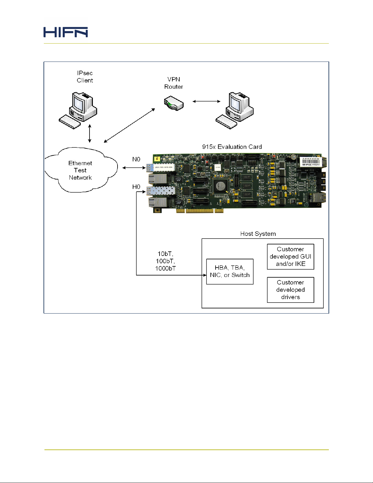
Figure 1-1. Evaluation Card Typical Application
The intent of the evaluation card is to simulate the actual software environment of the end
system to the greatest extent possible. This is easily achieved due to the FlowThrough
nature of the Hifn 915x devices. From the host perspective, software commands sent out
the Ethernet port will be intercepted and acted upon just as if the chip were installed on the
same PCB as the host GMAC/TOE/Network Processor. Given this, the evaluation card can be
used to test virtually all of the customer-developed software at both the driver and the
application layers. This includes: boot-load, initialization, port control & monitoring,
fragment reassembly, and security management.
9150, 9155 Evaluation Card User Guide, UG-0210-00 Page 10
Hifn Confidential
Page 11
2 Overview
2.1 Card Layout
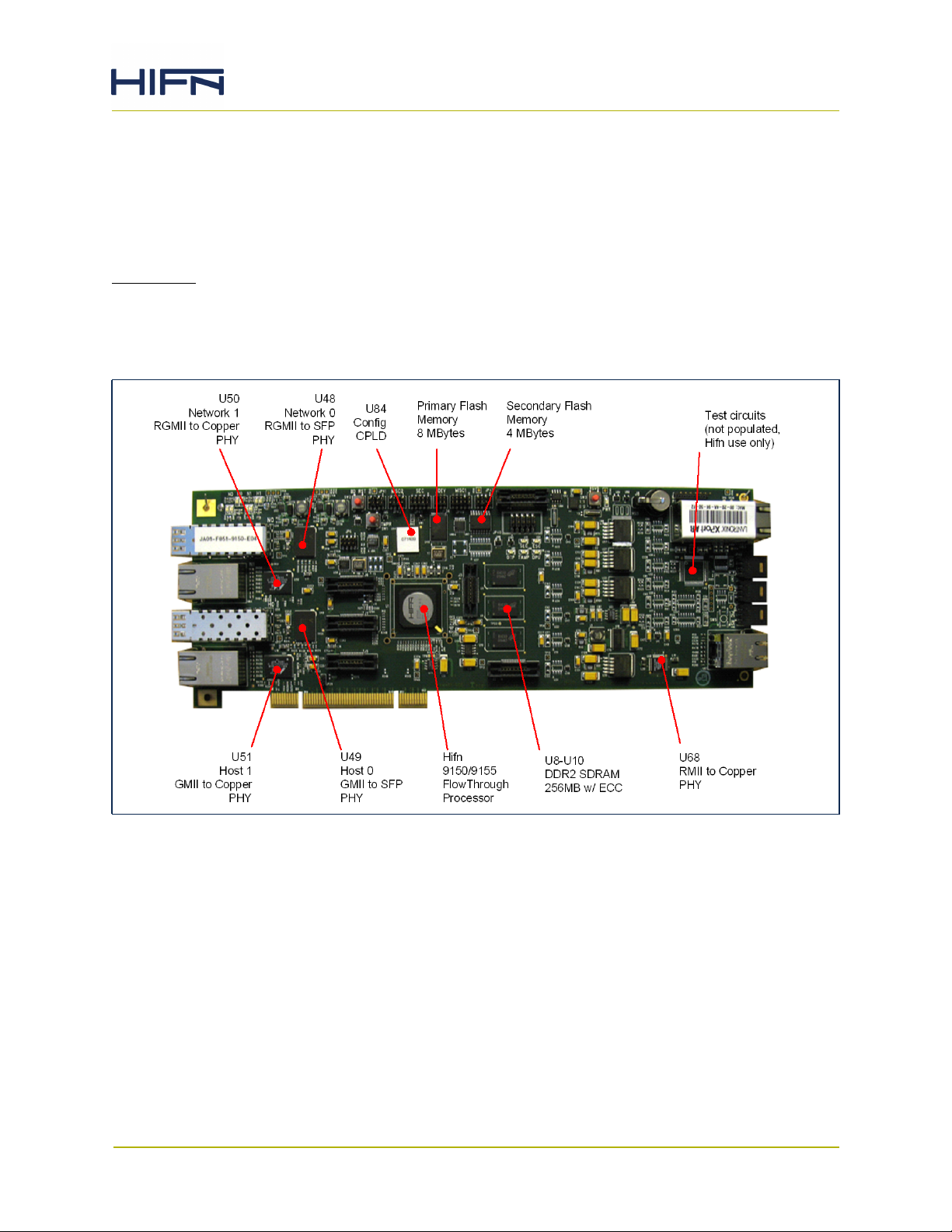
Figure 2-1 below identifies the significant functional components on the evaluation card
with the exception of the LEDs, jumpers, connectors, and switches, which are described
fully in a later chapter. The Hifn security processor chip is in the center of the card and
clearly labeled.
Figure 2-1. Evaluation Card Layout
9150, 9155 Evaluation Card User Guide, UG-0210-00 Page 11
Hifn Confidential
Page 12
2.2 Functional Overview
2.2.1 Block Diagram
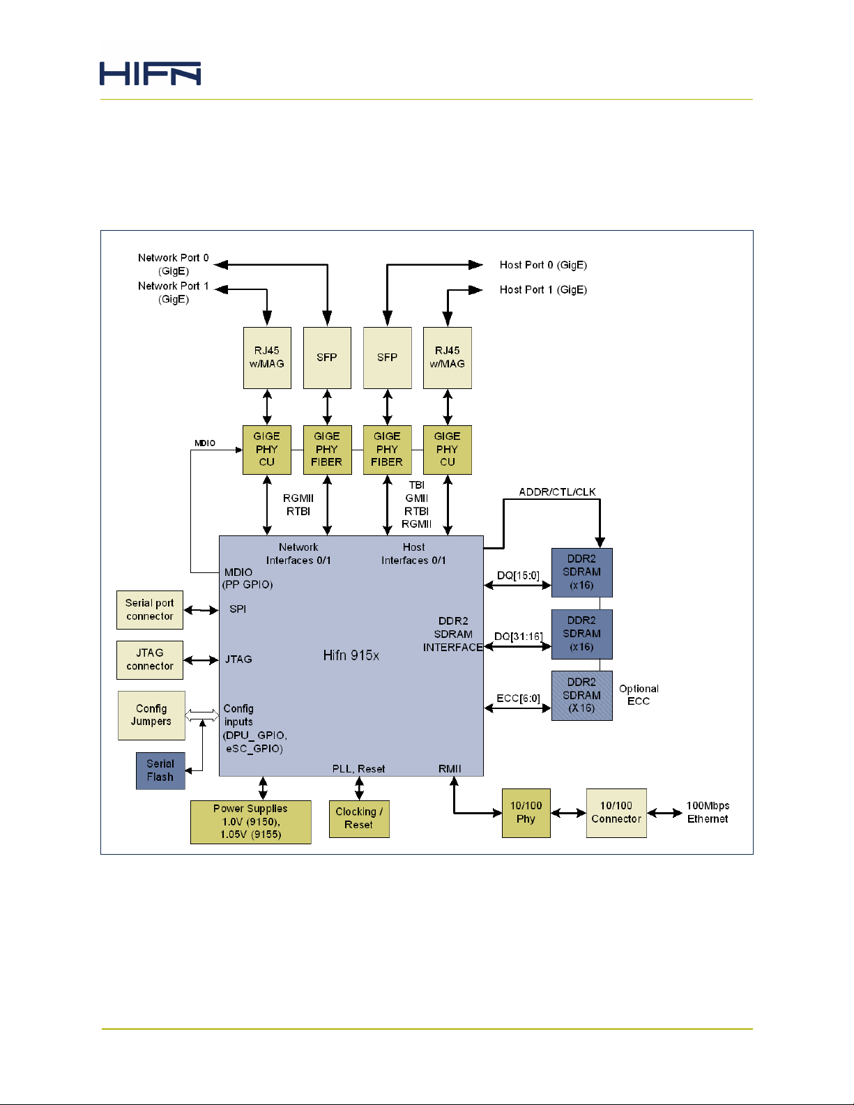
Figure 2-2. Evaluation Card Block Diagram
9150, 9155 Evaluation Card User Guide, UG-0210-00 Page 12
Hifn Confidential
Page 13
2.2.2 Hifn Security Processor Chip
At the heart of the evaluation card is the Hifn 915x applied services processor. The 915x
device combines high performance throughput, full Internet Key Exchange (IKE) support,
Internet Protocol Security (IPsec) support, and Internet Protocol Payload Compression
(IPComp) support with the intelligent packet processing functionality of Hifn's product
family.
Consult the 9150, 9155 Applied Services Processor Data Sheet and 9150, 9155 User Guide
for complete details on each device.
2.2.3 Gigabit Ethernet Interfaces
On this evaluation card, the Hifn applied services processor’s Gigabit Ethernet interfaces are
connected to either copper or fiber cabling environments through physical layer devices
(PHY) and connectors. For MAC-PHY connections to copper cabling and RJ45 connectors, the
Marvell 88E1111 PHY is used. For MAC-PHY connections to SFP connectors, the Vitesse
VSC8211 PHY is used. Refer to the table below for the combinations of PHY devices and
operating modes.
Table 2-1. PHY Device Operating Modes
Port Mode Connectivity Vendor Part Number
Network-0 RGMII SFP (Copper or Fiber) Vitesse VSC8211
Network-1 RGMII Copper (RJ45) Marvell 88E1111
Host-0 GMII SFP (Copper or Fiber) Vitesse VSC8211
Host-1 GMII Copper (RJ45) Marvell 88E1111
The evaluation card also supports other interface modes including TBI and SERDES. Please
note, however, that support for other interfaces requires card modifications that should not
be attempted by the user.
Each of the four gigabit Ethernet interfaces is accessible for debug or monitoring through a
high-density test connector (Amp MICTOR series) that easily interfaces to a logic analyzer.
Use of these connectors is discussed in a later section.
2.2.4 Flash Memory Interface
The eSC (sometimes referred to as the AP) is an embedded RISC core in the 915x chip that
is used to perform functions such as error and exception handling, and IKE processing. This
processor core on the evaluation card has access to the external flash memory devices
described in this section.
Flash memory can be used to store processor boot images, configuration data for other oncard devices such as network physical layer devices, and code development/storage. A flash
write utility is provided with the 915x SDK to allow code images and configuration data to
be written to flash.
9150, 9155 Evaluation Card User Guide, UG-0210-00 Page 13
Hifn Confidential
Page 14

The flash memory devices on the evaluation card are designed to be compatible with the 4wire SPI serial interface which is composed of the following signals: chip select, clock, serial
data in, and serial data out. These signals are shared with other chip functions on the eSC
processor's GPIO pins. The eSC flash memory interface signals are also available for debug
on one of the MICTOR debug connectors as shown in Section 3.4.
Flash Memory Devices
Two styles of flash memory devices are provided on the 915x Evaluation Card.
The two different flash memory devices are configured on the evaluation card as primary
flash and secondary flash. The terms ‘primary’ and ‘secondary’ are used to distinguish
which flash is connected to FLASH_CS0 (ESC_GPIO[0]) and FLASH_CS1 (ESC_GPIO[4]).
Selection of the primary and secondary flash can be configured through the MISC-2 header
as described in Section 4.1.4. The default configuration has the primary flash assigned to
an 8-MByte Atmel device (AT45DB642D) and secondary flash assigned to a 4-MBytes Atmel
device (AT25DF321).
Please note that the 915x security processor requires a minimum of 8MB when the flash
interface is utilized. Due to this requirement, the AT25DF321 is no longer recommended.
2.2.5 DDR2 SDRAM Interface
Each of the embedded 915x processor cores (DPU, eSC, PCP) has access to external DDR2
SDRAM memory. The 915x chip supports up to 512 Mbytes of DDR2 SDRAM memory,
excluding the optional ECC.
The 915x Evaluation Card is shipped with 256 MBytes of DDR2 SDRAM memory. The DDR2
SDRAM interface is available for debug and monitoring on Amp MICTOR-style connectors
(one for address/control, one for data). Note that the DDR2 SDRAM interface signals are
high speed SSTL-18 signals, and appropriate adapters and test equipment must be used
when probing these signals.
2.2.6 RMII Fast Ethernet Interface
The 915x Evaluation Card includes a general purpose RMII (100 Mbps) Ethernet MAC
interface. This interface may be used for out-of-band boot load, chip initialization and
management, as well as for inter-chip communications when multiple chips are used to
scale the performance or port count. All of the management features that can be
accomplished “in-band” over the host side GMAC ports can also be accomplished via the
RMII port.
Note
The RMII port is intended only for local communications between 915x devices or to a
control processor. It is NOT intended to be connected to a network interface since it does
not support the requisite networking features that would be required such as unique MAC
addressing, ARP, etc.
The MII interface consists of the seven RMII signals, a Fast Ethernet PHY transceiver, and
an integrated magnetics-RJ45 connector module.
9150, 9155 Evaluation Card User Guide, UG-0210-00 Page 14
Hifn Confidential
Page 15

2.2.7 JTAG Interface
The JTAG (Joint Test Action Group) interface provides access to the boundary-scan logic
within the 915x devices. The boundary-scan logic is used for testing the interconnections
between the 915x and other integrated circuits on the printed circuit card at manufacturing
time. The boundary-scan logic is compliant with the IEEE 1149.1 standard for boundaryscan testing. In addition, the JTAG interface is used for chip manufacturing tests and is also
used by Hifn for developing and debugging the firmware for the embedded processors. The
JTAG connector and pin descriptions are shown in a later chapter.
The JTAG circuit in the 915x device has a Chip ID and a Revision ID that is used by the test
equipment to identify the device and revision level in order to run the appropriate test
patterns. The following table shows the JTAG Chip and Revision IDs for the 915x devices.
Table 2-2. JTAG Chip and Revision IDs
Model JTAG Chip ID JTAG Revision ID
915x 0x0002526D 0x02
2.2.8 CPLD Interface
In order to easily configure the evaluation card for a variety of interface options and test
configurations, a CPLD (complex programmable logic device) is used to provide the majority
of connectivity for pins used for chip configuration including GPIO. Although there is no
customer access to the CPLD internal logic elements, a brief summary of the CPLD functions
is included here for Hifn professionals:
• Host/Network Link and Activity LED Mux
• 3-Way Mux for all GPIO pins (Reset Capture, Primary Usage, and Disconnect for PC
Mode
• Control of all 915x config pins (PLL_MODE, DDR2_CONFIG, GMAC_CONFIG, etc)
• Interface for Lantronix XPORT-AR module
• Interface to SFP modules
• Interface to Flash Memory, Ds3641, and RTC chips
2.2.9 GPIO Interface
The eSC and DPU embedded processor cores both contain 16-bit external GPIO (General
Purpose Input/Output) buses that can be used for functions such as boot mode
configuration, Flash memory connectivity, or customer-specific functions. All GPIO pins
default to inputs and are sampled following reset for various configuration purposes.
Internal registers accessed by the eSC and DPU processors control the I/O direction of each
pin. Other internal registers are used to read the GPIO pin states when they are inputs or
set their state when they are an output.
9150, 9155 Evaluation Card User Guide, UG-0210-00 Page 15
Hifn Confidential
Page 16
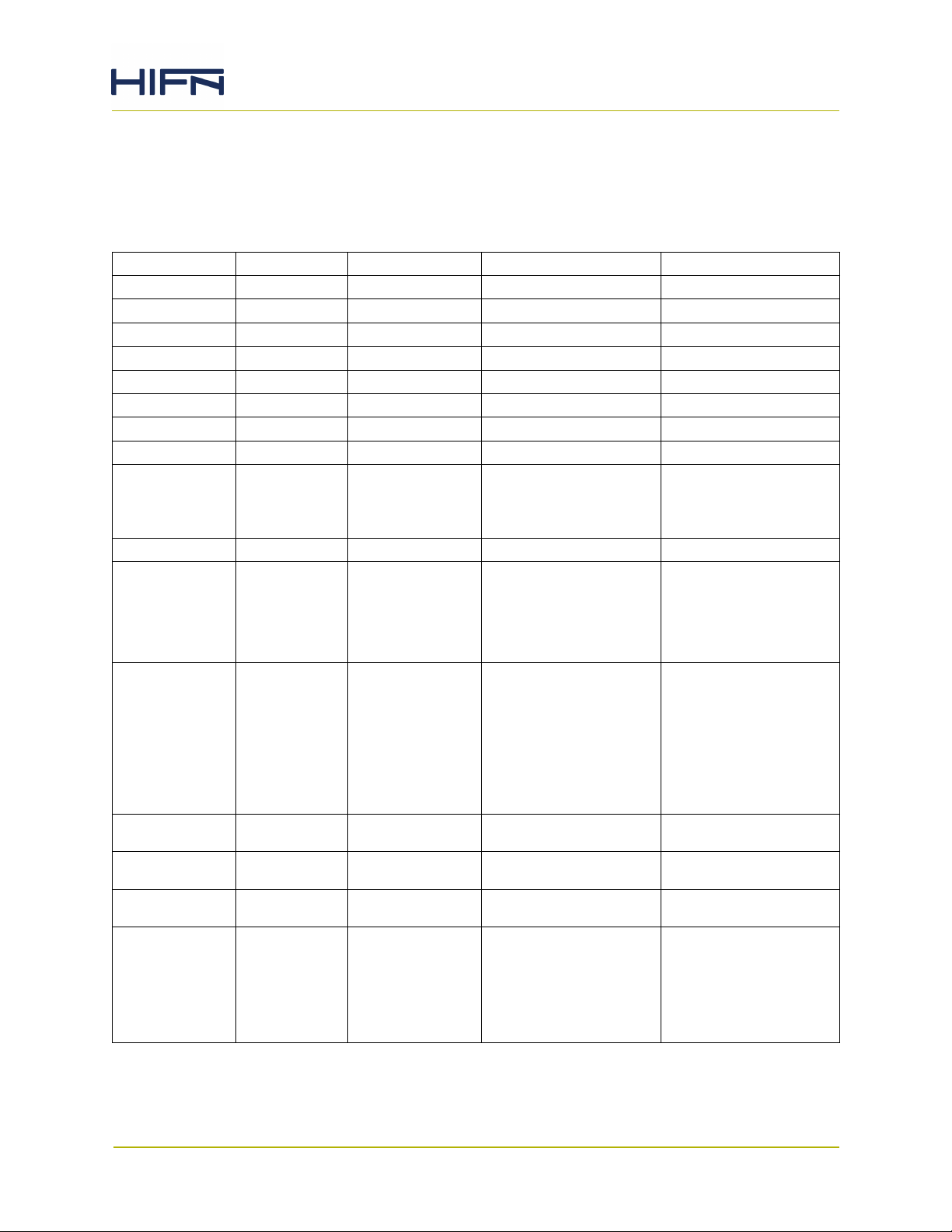
Most of the GPIO pins have pre-defined functions as shown in the table below. These
functions are subject to change, so the user should consult the latest data sheet revision
applicable to the Hifn device selected for detailed and accurate GPIO descriptions.
Table 2-3. General Purpose I/O Pins
Signal Name Primary Use Reset Capture Reset Capture Function Card Connection
dpu_gpio[15] Host1_Link Unused Unused CPLD (LED Mux)
dpu_gpio[14] Host0_Link Unused Unused CPLD (LED Mux)
dpu_gpio[13] Host1_Act Unused Unused CPLD (LED Mux)
dpu_gpio[12] Host0_Act Unused Unused CPLD (LED Mux)
dpu_gpio[11] Net1_Link Unused Unused CPLD (LED Mux)
dpu_gpio[10] Net0_Link Unused Unused CPLD (LED Mux)
dpu_gpio[9] Net1_Act Unused Unused CPLD (LED Mux)
dpu_gpio[8] Net0_Act Unused Unused CPLD (LED Mux)
dpu_gpio[7] DPU Status
LED
1=LED on
0= LED off
dpu_gpio[6] MDIO/SDA Unused Unused GPIO Mux
dpu_gpio[5] MDC/SCL serdes_hidrv 0=tx_lvl[4:0] should
dpu_gpio[4] Net0
TX_DISABLE
dpu_gpio[3] Net1
TX_DISABLE
dpu_gpio[2] Net0
RX_LOSS
dpu_gpio[1] Net1
RX_LOSS
dpu_gpio[0] Secure Mode
LED
Unused Unused CPLD (LED Driver)
be set to 5'b 01000
(1.0v transmit level)
1=tx_lvl[4:0] should
be set to 5'b 11000
(1.16v transmit level)
ddr_config_1 ddr_config_1:
ddr_config[1:0]
determines the size of
the installed DDR2
SDRAM memory
00=64MB
01=128MB
10=256MB
11=512MB
ddr_config_0 ddr_config_0 CPLD (GPIO Mux)
RGMII Voltage
Level
boot_config_1 1=Flash, 0=No Flash CPLD (GPIO Mux)
boot_config_0 0=All PPCI commands
1=1.5V HSTL, 0=2.5V
LVCMOS
received over Host0 /
Host1 will be
discarded.
1=Accept PPCI
commands over Host0
/ Host1
GPIO Mux
CPLD (GPIO Mux)
CPLD (GPIO Mux)
CPLD (GPIO Mux)
9150, 9155 Evaluation Card User Guide, UG-0210-00 Page 16
Hifn Confidential
Page 17
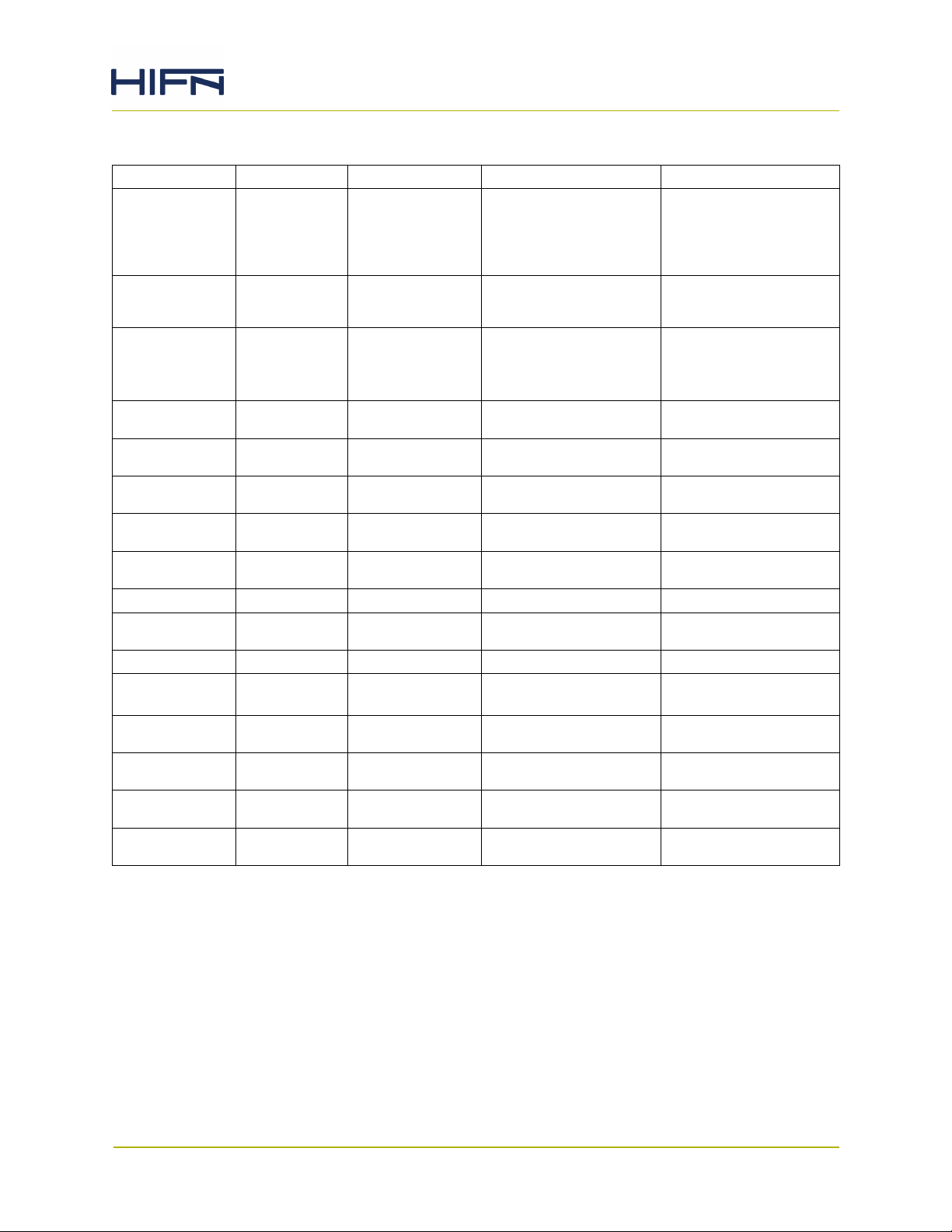
Table 2-3. General Purpose I/O Pins
Signal Name Primary Use Reset Capture Reset Capture Function Card Connection
esc_gpio[15] eSC_gpio
[15]
esc_gpio[14] OTP_VPP_EN_NUnused Active low signal to
esc_gpio[13] CAPTURE_
COMPLETE
esc_gpio[12] eSC_gpio
[12]
esc_gpio[11] eSC_gpio
[11]
esc_gpio[10] eSC_gpio
[10]
esc_gpio[9] eSC_gpio[9] Secure_Feature
esc_gpio[8] eSC_gpio[8] Secure_Feature
esc_gpio[7] eSC Status Unused Unused CPLD (LED Driver)
esc_gpio[6] PHY
Interrupt
esc_gpio[5] Flash_CS2 Device_ID[1] Device_ID[1] CPLD (GPIO Mux)
esc_gpio[4] eSC_Flash_C
S1/I
2
C Data
esc_gpio[3] eSC_Flash_SORMII MAC/PHY 1=PHY, 0=MAC CPLD (GPIO Mux)
MemClr 0=Some parts of
CPLD (GPIO Mux)
SRAM left uncleared
during soft reset
1=Clear SRAM
memory during reset
CPLD
control the OTP_VPP
voltage
Unused 0=reset capture not
CPLD
complete
1=reset capture
complete
Secure_Feature
Reserved CPLD (GPIO Mux)
[4]
Secure_Feature
Reserved CPLD (GPIO Mux)
[3]
Secure_Feature
Reserved CPLD (GPIO Mux)
[2]
Suite B Only CPLD (GPIO Mux)
[1]
Bypass Disable CPLD (GPIO Mux)
[0]
Device_ID[2] Device_ID[2] CPLD (GPIO Mux)
Device_ID[0} Device_ID[0} GPIO Mux
esc_gpio[2] eSC_Flash_SI100M/1G Boot 1= 100M boot, 0= 1G
CPLD (GPIO Mux)
boot
esc_gpio[1] eSC_Flash_
Unused Unused GPIO Mux
CLK
esc_gpio[0] eSC_Flash_
Unused Unused CPLD (GPIO Mux)
CS0
9150, 9155 Evaluation Card User Guide, UG-0210-00 Page 17
Hifn Confidential
Page 18
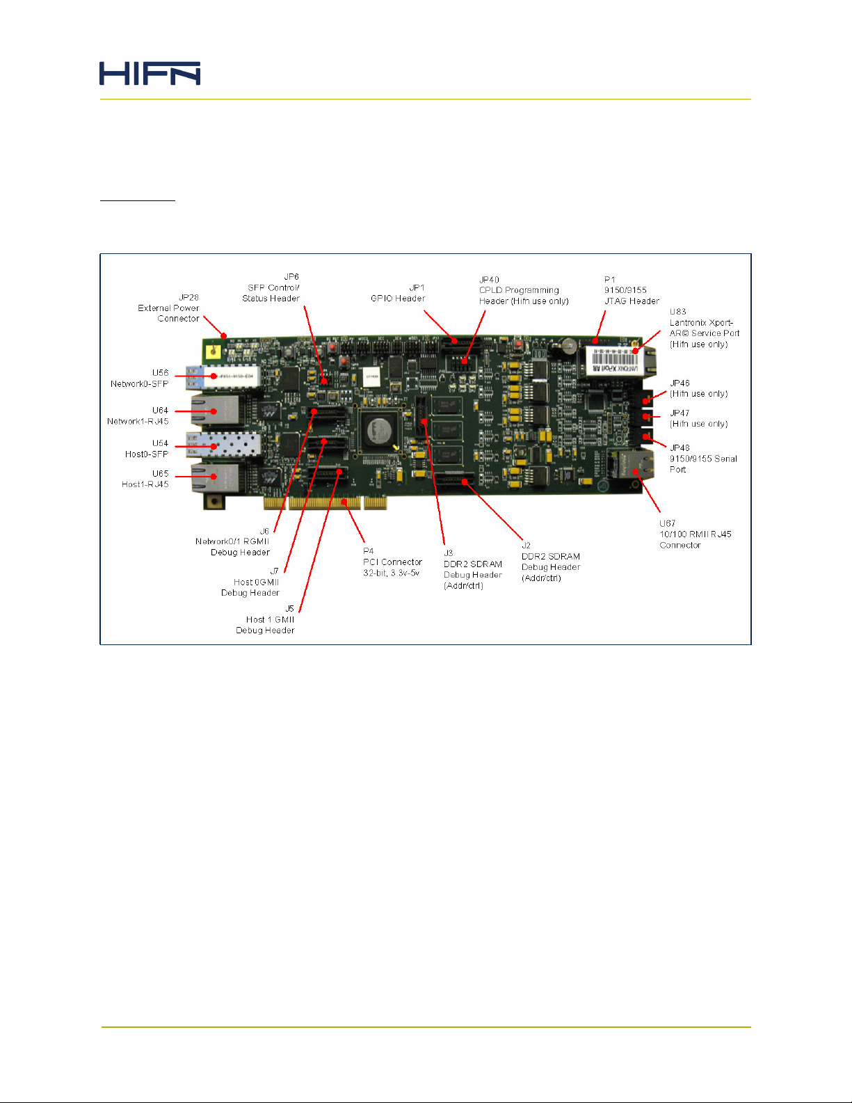
3 Connectors
Figure 3-1 illustrates the location of the power and signal connectors on the 915x
Evaluation Card:
Figure 3-1. 915x Evaluation Card Connectors
3.1 Power Connectors
The 915x Hifn Evaluation Card can be powered from either an external power supply or
through the PCI connector. Two voltages are required for proper operation: +5V and
+3.3V.
3.1.1 JP28: External Power Supply Connector
A four-pin plastic power connector is provided in the upper left-hand corner on the back
side of the card. The connector style is right-angle disk-drive style power connector and
uses a Molex connector PN 53109-0410. A suitable mating receptacle is the
AMP 1-480424-0. The pins are numbered from 1 to 4 on the PCB, from left to right, with
9150, 9155 Evaluation Card User Guide, UG-0210-00 Page 18
Hifn Confidential
Page 19
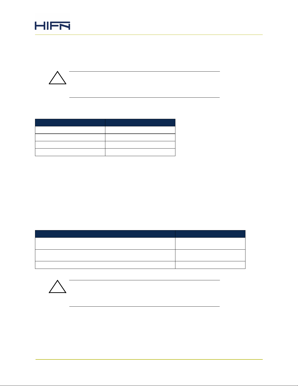
pin 1 of the connector associated with the only square pad on the PCB footprint. A standard
PC power supply can be modified to include the mating connector and must include the
connections listed in the table below.
!
Caution
Do not use un-modified disk-drive power cable as this will result
in catastrophic damage to the card.
Table 3-1. External Power Supply Connections
Pin Number Description
1 +3.3V
2 GND
3 GND
4 +5V
3.1.2 P4: PCI Connector
A PCI connector is available solely for the purposes of providing an alternative power
source. There are no other PCI connections provided, so slot assignment is not an issue as
long as +3.3V and +5.5V are provided as per the following table.
Note
PRSNT1* and PRSNT2* are grounded through 0-ohm resistors on the evaluation card.
Table 3-2. PCI Power Pin Assignment
Pin Number Description
A21, B25, A27, B31, A33, B36, A39, B41, B43, A45, A53,
B54
B3, A12, B12, A13, B13, B15, B17, A18, B22, A24, B28,
A30, B34, A35, A37, B38, A42, B46, A48, A56, B57
A5, B5, B6, A8, A61, B61, A62, B62 +5V
Caution
+3.3V
GND
!
Do not reverse polarity on power connections. Possible damage
to the card may result
3.2 Ethernet Connectors
Four Gigabit Ethernet interfaces and one RMII 100Mbps Ethernet interface exist on this
card.
9150, 9155 Evaluation Card User Guide, UG-0210-00 Page 19
Hifn Confidential
Page 20
3.2.1 U54, U56: SFP Connectors
The Host-0 and Network-0 network ports are configured as SFP ports (Small FormFactor
Pluggable). On-card Gigabit Ethernet PHY devices provide the necessary GMII/TBI/RGMII/
RTBI and embedded SERDES interfaces to receive and transmit data on these ports to and
from the Hifn security processor. SFP ports are physically composed of a 20-pin surfacemount connector that is encased in a metal cage that provides some amount of heat
transfer and EMI protection. Note that this evaluation card is not designed to comply with
any EMI susceptibility or interference standards. Though SFP ports were originally designed
for use in optical networking, SFP transceivers are now available which support copper
cabling (RJ45-style connectors).
There are many suppliers for SFP transceivers, and the minimum requirements for their use
with this evaluation card are: 3.3V, 1.250 Gbps. The following transceivers have been used
successfully at Hifn and may be ordered through Hifn along with the evaluation card.
Table 3-3. SFP Transceiver Modules
Hifn SKU Number Part Number Description
SFP FTRJ-8619 Finisar Short Wavelength (850nm) SFP Transceiver
SFP FCMJ-8521 Finisar 1000Base-T Copper SFP Transceiver
Each of the SFP modules' internal EEPROMs and registers are accessible through a two-wire
serial interface (I2C via GPIO) that is connected through the on-card CPLD device. Since all
SFP modules are hard-wired for the same I2C address, the evaluation card also includes an
I2C mux that can be accessed via I2C commands. Please contact Hifn for further details on
GPIO-driven SFP communication.
3.2.2 U64, U65, U67: RJ45 Connectors
The Host-1 and Network-1 network ports and the RMII port are configured with RJ45
connectors that provide copper Ethernet connectivity with the vast majority of network
infrastructures.
Please note that the RMII port is not intended to be connected to a generic LAN since it
does not support the requisite networking features that would be required such as unique
MAC addressing, ARP, etc. Rather, it is intended to connect to the customer's host control
processor running specialized code for managing the 915x chip. Refer to the 9150, 9155
User Guide, UG-0195 for further information.
3.3 P1: JTAG Connector
Access to the Hifn security processor’s JTAG interface is accomplished through an on-card
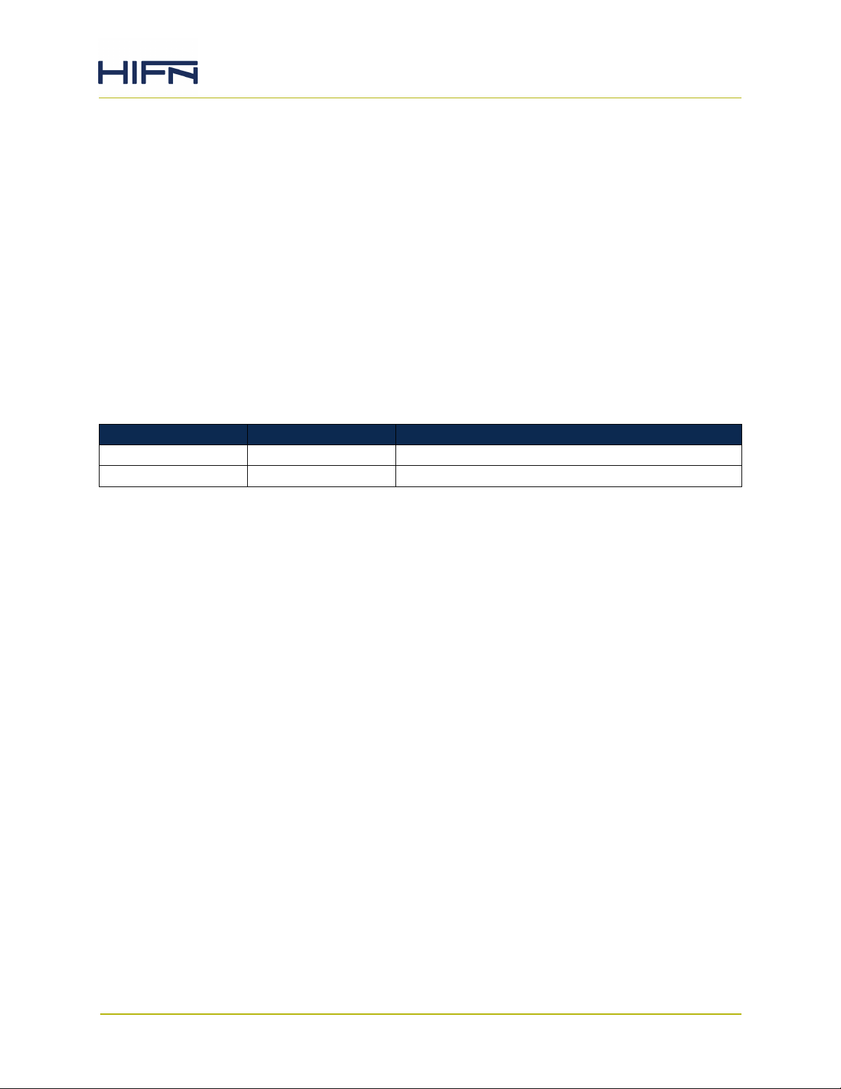
seven-pin single-in-line header at location P1. To support the more common two-row by 5pin JTAG connector, a simple transition header can be assembled (contact Hifn for further
information). The JTAG connector's pins are numbered 1 through 7 from top to bottom, and
the JTAG signals are assigned to those pins as shown in the following table.
9150, 9155 Evaluation Card User Guide, UG-0210-00 Page 20
Hifn Confidential
Page 21
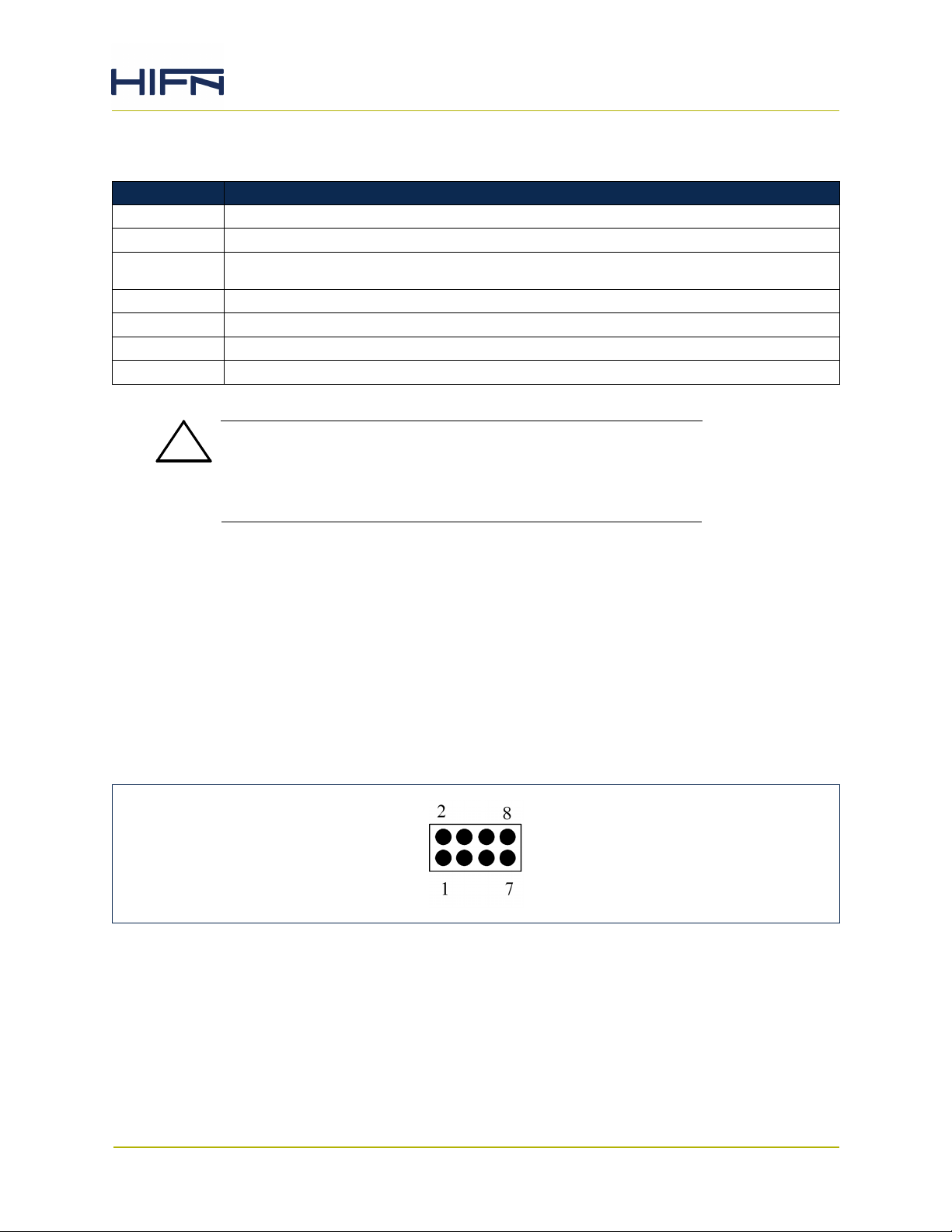
Table 3-4. JTAG Connector Pinout
Pin Number Description
1 +3.3V
2 GND
3 JTAG_RST*: This signal is not supported in the Hifn security chip and should be
4 JTAG_TCK: JTAG Test Clock
5 JTAG_TDI: JTAG Test Data Input
6 JTAG_TDO: JTAG Test Data Output
7 JTAG_TMS: JTAG Test Mode Select
left unconnected.
!
Caution
Care must be taken when attaching cables to the JTAG header.
Misalignment of the connector and cable could result in a short
between power and ground, and cause card damage.
3.4 Debug Connectors
3.4.1 JP6: SFP Control/Status
This header can be used to monitor status signals driven by the SFP modules and also to
communicate with the serial EEPROM and PHY devices inside the SFP modules. Hifn has
successfully configured SFP modules for SGMII operation using this header along with some
3rd party hardware/software for I2C emulation. Contact Hifn for further details on
configuring SFP modules for SGMII operation.
Figure 3-2. SFP Connector Diagram
9150, 9155 Evaluation Card User Guide, UG-0210-00 Page 21
Hifn Confidential
Page 22
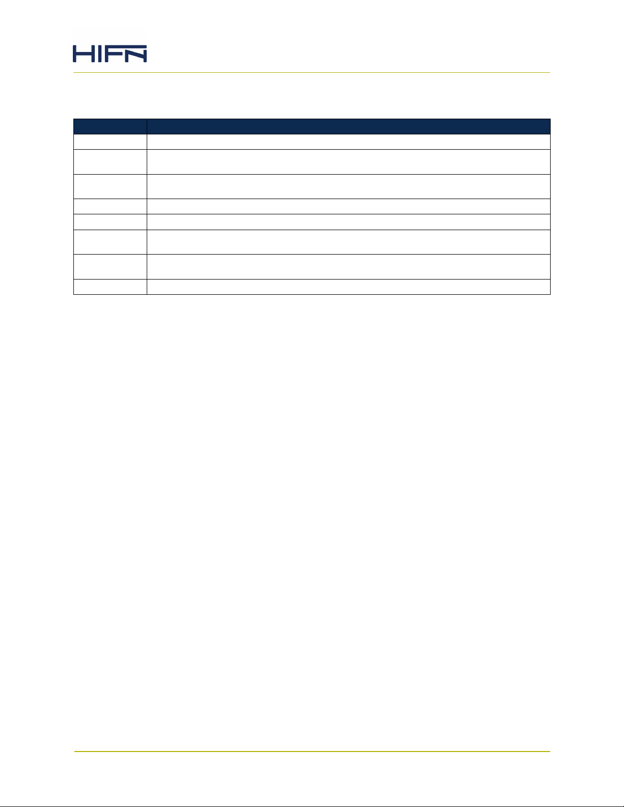
Table 3-5. SFP Control/Status Connector
Pin Number Description
1 H0_SFP_MOD0 (Module Present, Grounded inside SFP module)
2 H0_SFP_MOD1_SCL (Clock signal for two-wire serial interface to SFP's EEPROM
3 H0_SFP_MOD2_SDA (Data signal for two-wire serial interface to SFP's EEPROM
4 H0_SFP_FAULT (When high, indicates laser fault)
5 N0_SFP_MOD0 (Module Present, Grounded inside SFP module)
6 N0_SFP_MOD1_SCL (Clock signal for two-wire serial interface to SFP's EEPROM
7 N0_SFP_MOD2_SDA (Data signal for two-wire serial interface to SFP's EEPROM
8 N0_SFP_FAULT (When high, indicates laser fault)
and PHY registers)
and PHY registers)
and PHY registers)
and PHY registers)
3.4.2 Amp MICTOR Headers
High-density connectors and probe adapters facilitate access to most interfaces on the
evaluation card.
The illustration below is an excerpt from the Agilent Technologies document “Probing
Solutions for Logic Analysis Systems” and shows how the logic analyzer pod is connected to
a PCB. Note that the 38-pin MICTOR connector is surface-mounted on the evaluation card.
It should also be noted that the connector includes through-hole ground pins, which
provides good noise immunity.
9150, 9155 Evaluation Card User Guide, UG-0210-00 Page 22
Hifn Confidential
Page 23
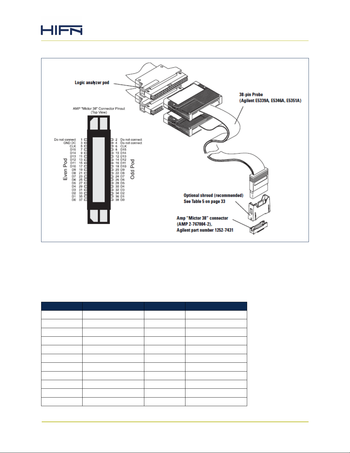
Figure 3-3. Debug Connector Usage
MICTOR connectors are used widely in the computer industry for achieving debug access in
high-density designs. The connector is available at TYCO-AMP (pn: 2-767004-2), and the
logic analyzer probe adapter is available through Agilent (pn E5346A).
Table 3-6. J6: Net-0/Net-1Gigabit Port
Pin Number Signal Pin Number Signal
1NC 2NC
3 GND 4 NC
5 N0_TXC 6 N1_TXC (Note 1)
7 N0_SFP_RLOS 8 NC
9 N0_PHY_SDET 10 NC
11 NC 12 NC
13 N0_TXD4 14 N1_TXD4
15 N0_TXD3 16 N1_TXD3
17 N0_TXD2 18 N1_TXD2
19 N0_TXD1 20 N1_TXD1
21 N0_TXD0 22 N1_TXD0
9150, 9155 Evaluation Card User Guide, UG-0210-00 Page 23
Hifn Confidential
Page 24
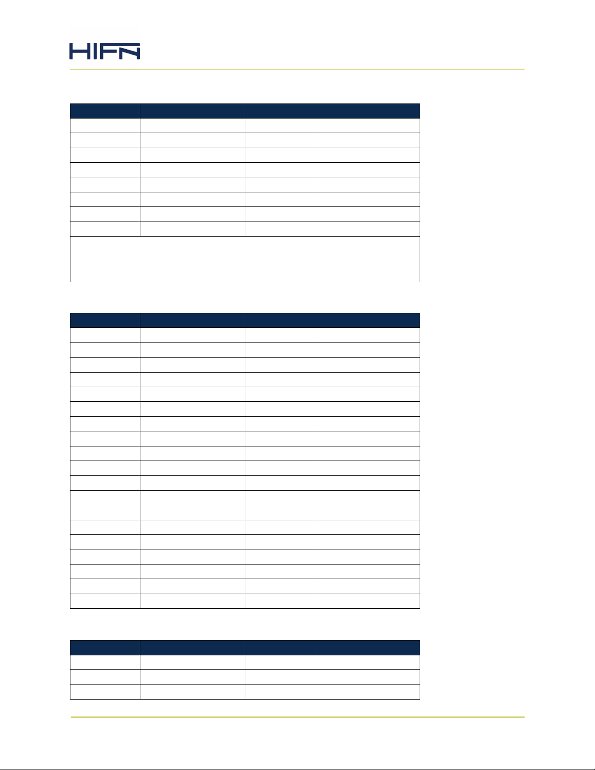
Table 3-6. J6: Net-0/Net-1Gigabit Port
Pin Number Signal Pin Number Signal
23 NC 24 NC
25 NC 26 NC
27 NC 28 NC
29 N0_RXD4 30 N1_RXD4
31 N0_RXD3 32 N1_RXD3
33 N0_RXD2 34 N1_RXD2
35 N0_RXD1 36 N1_RXD1
37 N0_RXD0 38 N1_RXD0
Notes:
1. Both clock ports on the Net-0/Net-1 debug connector can be configured
for N0_RXC and N1_RXC through simple on-card resistor changes.
Please contact Hifn for further details.
Table 3-7. J5: Host-1 Gigabit Port
Pin Number Signal Pin Number Signal
1NC 2NC
3 GND 4 NC
5 H1_GTXCLK 6 H1_PHY_REFCLK
7NC 8NC
9 NC 10 H1_CRS
11 NC 12 H1_COL
13 NC 14 NC
15 H1_TXCTL 16 H1_RXCTL
17 NC 18 NC
19 H1_TXD9 20 H1_RXD9
21 H1_TXD8 22 H1_RXD8
23 H1_TXD7 24 H1_RXD7
25 H1_TXD6 26 H1_RXD6
27 H1_TXD5 28 H1_RXD5
29 H1_TXD4 30 H1_RXD4
31 H1_TXD3 32 H1_RXD3
33 H1_TXD2 34 H1_RXD2
35 H1_TXD1 36 H1_RXD1
37 H1_TXD0 38 H1_RXD0
Table 3-8. J7: Host-0 Gigabit Port
Pin Number Signal Pin Number Signal
1NC 2NC
3 GND 4 NC
5 H0_GTXCLK 6 H0_PHY_REFCLK
9150, 9155 Evaluation Card User Guide, UG-0210-00 Page 24
Hifn Confidential
Page 25
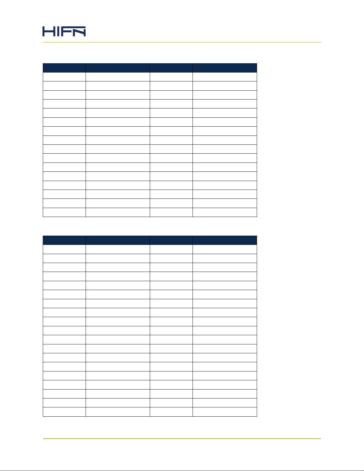
Table 3-8. J7: Host-0 Gigabit Port
Pin Number Signal Pin Number Signal
7 H0_SFP_RLOS 8 H0_PHY_SIGDET
9 NC 10 H0_CRS
11 NC 12 H0_COL
13 NC 14 NC
15 NC 16 H0_RXCTL
17 H0_TXD9 18 NC
19 H0_TXD8 20 H0_RXD9
21 H0_TXD7 22 H0_RXD8
23 H0_TXD6 24 H0_RXD7
25 H0_TXD5 26 H0_RXD6
27 H0_TXD4 28 H0_RXD5
29 H0_TXCTL 30 H0_RXD4
31 H0_TXD3 32 H0_RXD3
33 H0_TXD2 34 H0_RXD2
35 H0_TXD1 36 H0_RXD1
37 H0_TXD0 38 H0_RXD0
Table 3-9. J1: System Interfaces
Pin Number Signal Pin Number Signal
1NC 2NC
3 GND 4 NC
5 DPU_GPIO_15 6 NC
7 DPU_GPIO_15 8 MDIO
9 DPU_GPIO_14 10 MDC
11 DPU_GPIO_13 12 PHY_INTERRUPT
13 DPU_GPIO_12 14 SFP_SCL
15 DPU_GPIO_11 16 SFP_SDA
17 DPU_GPIO_10 18 NC
19 DPU_GPIO_9 20 NC
21 DPU_GPIO_8 22 NC
23 DPU_GPIO_7 24 ESC_GPIO7
25 DPU_GPIO_6 26 ESC_GPIO6
27 DPU_GPIO_5 28 ESC_GPIO5
29 DPU_GPIO_4 30 ESC_GPIO4
31 DPU_GPIO_3 32 ESC_GPIO3
33 DPU_GPIO_2 34 ESC_GPIO2
35 DPU_GPIO_1 36 ESC_GPIO1
37 DPU_GPIO_0 38 ESC_GPIO0
9150, 9155 Evaluation Card User Guide, UG-0210-00 Page 25
Hifn Confidential
Page 26
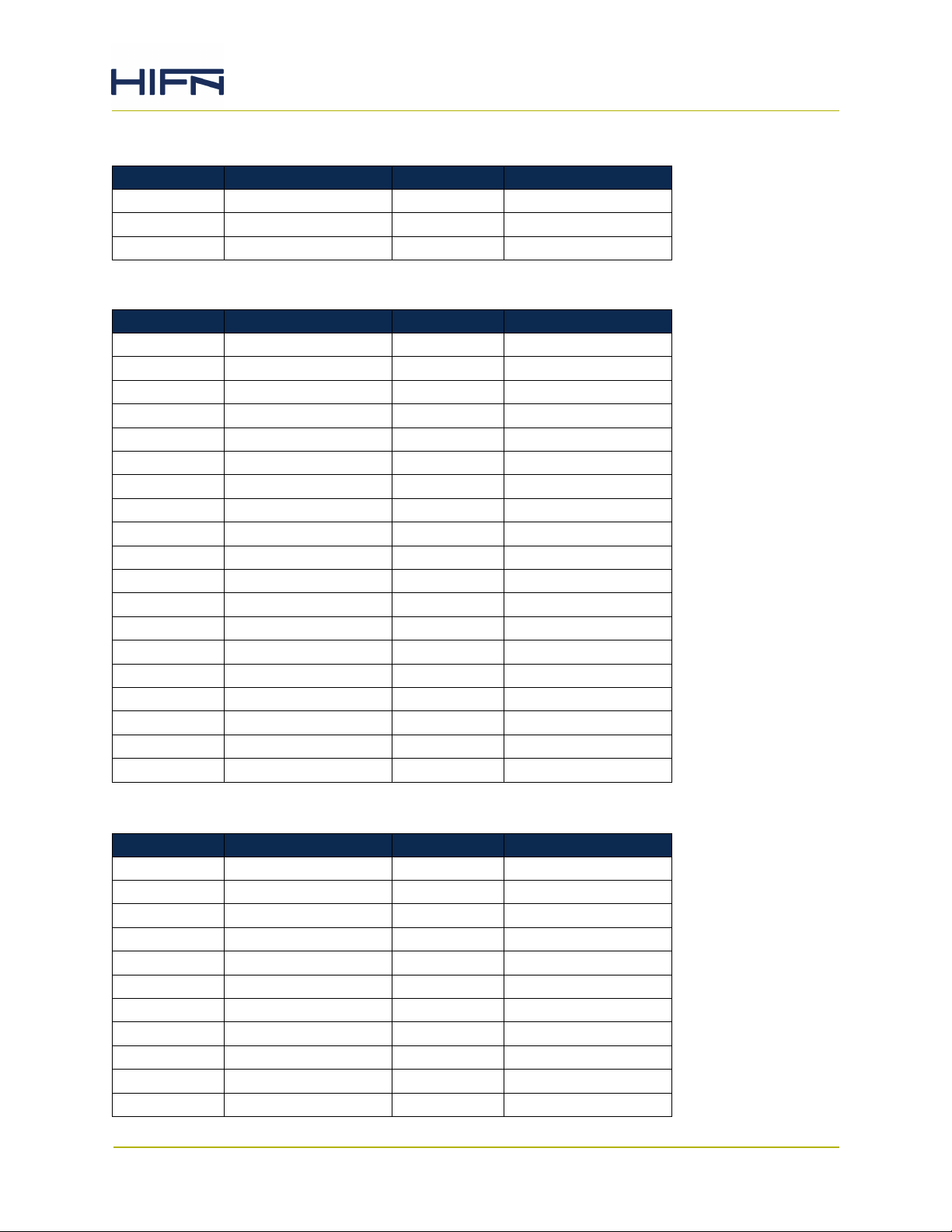
Table 3-9. J1: System Interfaces
Pin Number Signal Pin Number Signal
39 GND 40 GND
41 GND 42 GND
43 GND 44 NC
Table 3-10. J2: DDR2 Addr/Ctl
Pin Number Signal Pin Number Signal
1NC 2NC
3 GND 4 NC
5 DDR2_DIFFCLK_P 6 DDR2_DIFFCLK_N
7NC 8NC
9 DDR2_WE_N 10 NC
11 NC 12 NC
13 DDR2_BA2 14 DDR2_RAS_N
15 DDR2_CKE 16 DDR2_CAS_N
17 DDR2_BA0 18 DDR2_CS_N
19 DDR2_BA1 20 DDR2_ODT
21 NC 22 NC
23 DDR2_A10 24 DDR2_A6
25 DDR2_A5 26 DDR2_A2
27 DDR2_A1 28 DDR2_A0
29 NC 30 DDR2_A4
31 DDR2_A3 32 NC
33 DDR2_A12 34 DDR2_A11
35 DDR2_A7 36 DDR2_A8
37 DDR2_A9 38 DDR2_A13
Table 3-11. J3: DDR2 Data
Pin Number Signal Pin Number Signal
1NC 2NC
3 GND 4 NC
5NC 6NC
7 DDR2_DQ26 8 DDR2_DQ31
9 DDR2_DQ27 10 DDR2_DQ30
11 DDR2_DQ28 12 DDR2_DQ25
13 DDR2_DQ29 14 DDR2_DQ24
15 DDR2_DQ20 16 DDR2_DQ19
17 DDR2_DQ21 18 DDR2_DQ18
19 DDR2_DQ22 20 DDR2_DQ17
21 DDR2_DQ23 22 DDR2_DQ16
9150, 9155 Evaluation Card User Guide, UG-0210-00 Page 26
Hifn Confidential
Page 27
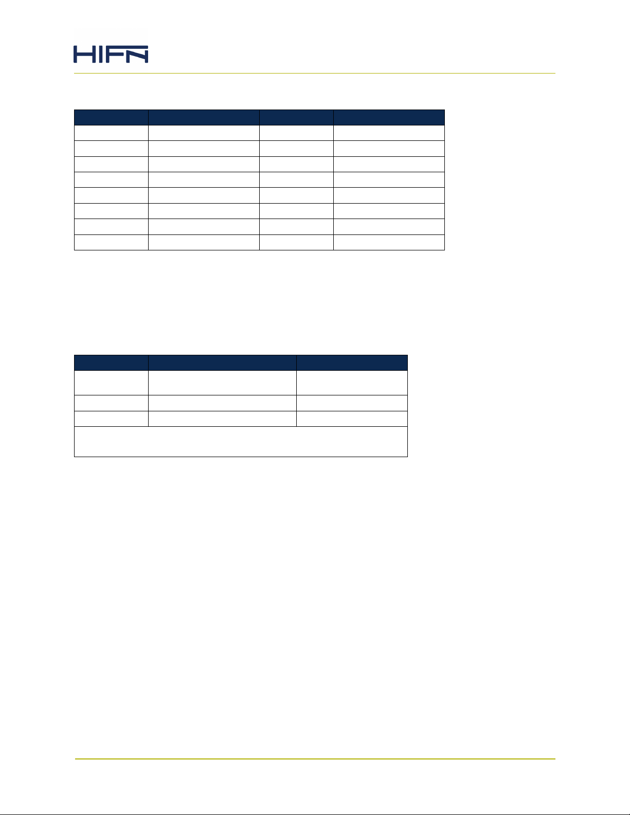
Table 3-11. J3: DDR2 Data
Pin Number Signal Pin Number Signal
23 DDR2_DQ10 24 DDR2_DQ15
25 DDR2_DQ11 26 DDR2_DQ14
27 DDR2_DQ12 28 DDR2_DQ9
29 DDR2_DQ13 30 DDR2_DQ8
31 DDR2_DQ4 32 DDR2_DQ3
33 DDR2_DQ5 34 DDR2_DQ2
35 DDR2_DQ6 36 DDR2_DQ1
37 DDR2_DQ7 38 DDR2_DQ0
U83: Lantronix XPOR-AR Module, Hifn Use Only
JP46, JP47: Hifn Use Only
JP40: CPLD Programming Header, Hifn Use Only
Table 3-12. JP48: 915x Serial Port
Pin Number Description Signal
1 Bottom pin, rectangular pad
on back of PCB
2 Center pin GND
3 Top pin TXOUT
3-pin right-angle rectangular connector, Amp 103361-1.
Mating connector is Amp 103976.
RXIN
9150, 9155 Evaluation Card User Guide, UG-0210-00 Page 27
Hifn Confidential
Page 28
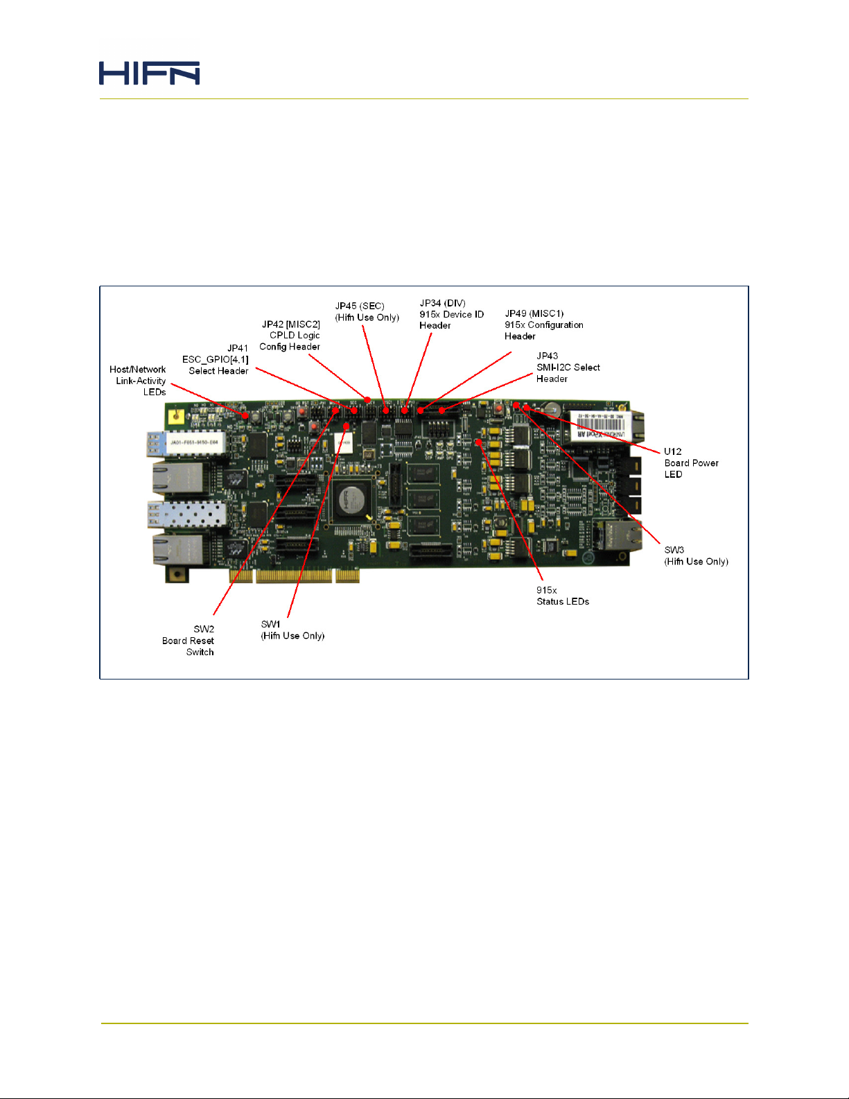
4 Jumpers, LEDs, and Switches
There are a number of jumpers on the 915x Evaluation Card. Most of these are factory set
and need not be re-configured. However, a few of the jumpers are user-configured to select
operating modes and settings. The following illustration identifies jumper locations,
switches, and LEDs on the evaluation card.
Figure 4-1. Jumpers, LEDs, and Switch Locations
4.1 Jumpers
Unless otherwise specified, the table values represent the following:
0: Jumper Installed
1: Jumper Not Installed
The text inside parenthesis represents the identification of the header in the silkscreen on
the PCB. Also, default manufacturing jumper settings are highlighted in bold.
9150, 9155 Evaluation Card User Guide, UG-0210-00 Page 28
Hifn Confidential
Page 29
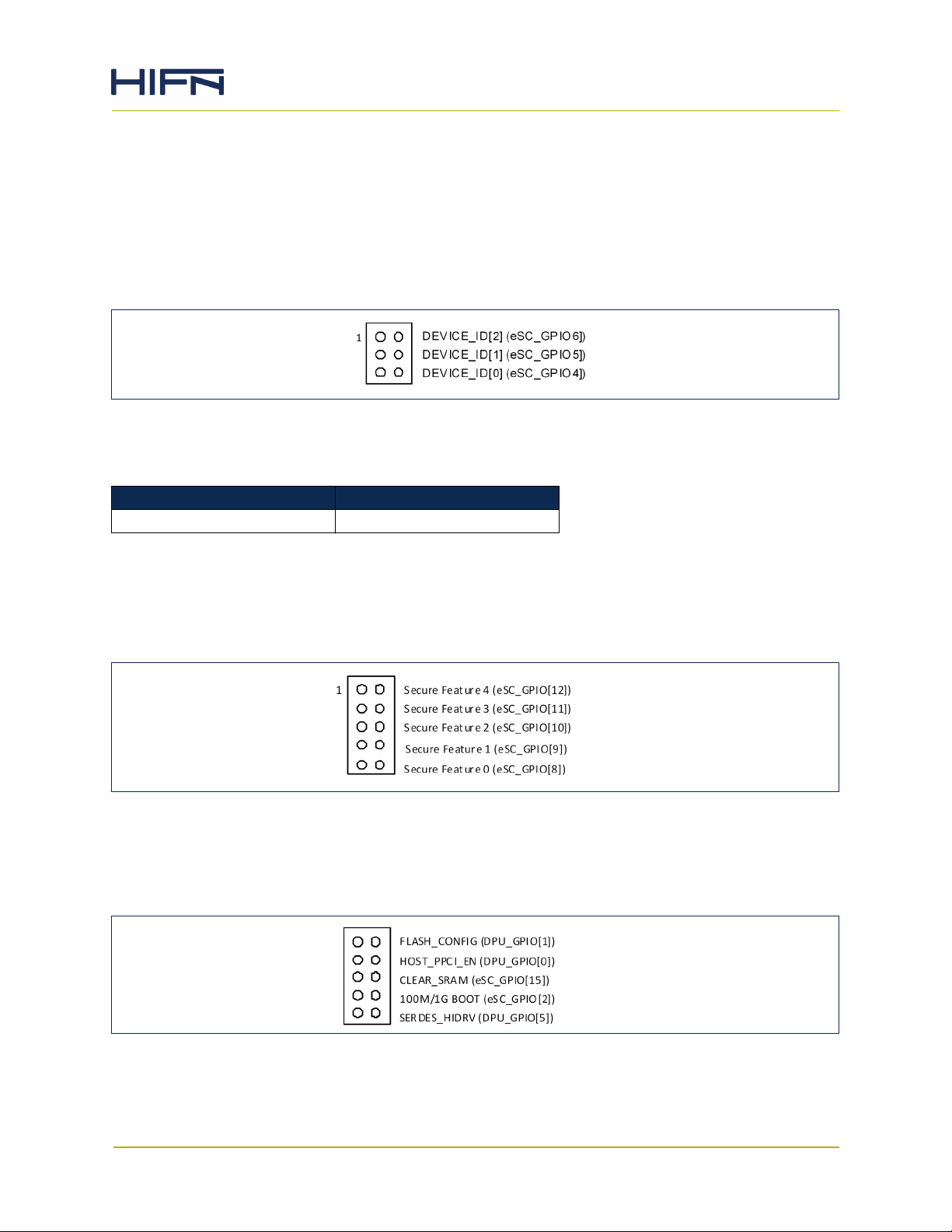
4.1.1 JP34: Device ID Header (DEV-ID)
This jumper header is used to uniquely identify each 915x chip in a multi-chip card
configuration. It has also been useful in development environments where multiple cards
are in the same system. These jumpers are typically not modified unless a development
system includes more than one evaluation card. In that case, these jumpers can be used to
uniquely identify each card.
Figure 4-2. JP34 Device ID Jumper Diagram
Table 4-1. Device ID Configuration Jumpers
Device_ID[2:0] Setting
000 Device ID = '000' (Default)
4.1.2 JP45: Secure Features Header (SEC)
These jumpers are for Hifn use only and should not be modified.
Figure 4-3. JP45 Secure Features Jumpers Diagram
4.1.3 JP49: System Configuration Header 1 (MISC-1)
Figure 4-4. JP49 System Configuration Header 1 Diagram
9150, 9155 Evaluation Card User Guide, UG-0210-00 Page 29
Hifn Confidential
Page 30
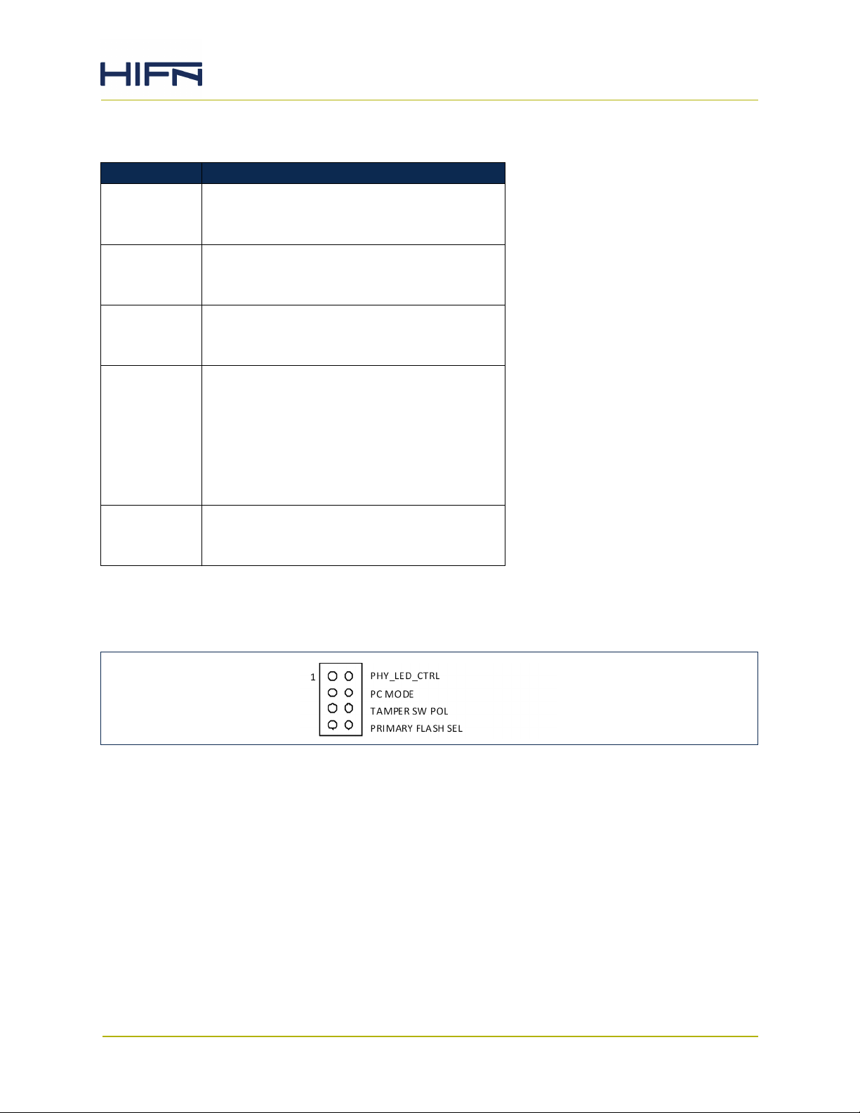
Table 4-2. JP49 System Configuration Header 1
Pin Number Description
1-2 Flash Configuration
0 = Ignore Flash
1 = Use Flash
3-4 Host PPCI Enable
0 = PPCI disabled
1 = PPCI enabled
5-6 Clear SRAM
0 = Clear SRAM
1 = Do not clear SRAM
7-8 100M/1G Boot Mode
For TBI, RTBI, SERDES and SGMII Modes:
0 = Enable Autonegotiate
1 = Disable Autonegotiate
For GMII, RGMII modes:
0 = 1G boot
1 = 100M boot
9-10 SerDes Transmit Level
0 = SerDes transmit level = 1.0V
1 = SerDes transmit level = 1.16V
4.1.4 JP42: System Configuration Header 2 (MISC-2)
Figure 4-5. JP42 System Configuration Header 2 Diagram
9150, 9155 Evaluation Card User Guide, UG-0210-00 Page 30
Hifn Confidential
Page 31
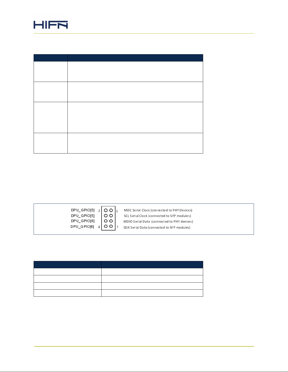
Table 4-3. JP42 System Configuration Header 2
Pin Number Description
1-2 PHY LED Control
0 = COMM LEDs are 915x driven
1 = COMM LEDs are PHY driven
3-4 PC Mode
0 = GPIO are used as I/O
1 = Reserved, customer must not modify
5-6 Tamper Switch Polarity
This jumper changes the way the on-card tamper switch is
handled inside the CPLD.
0 = [tamper_in_0_n] is asserted low when SW1 is closed
1 = [tamper_in_0] is asserted high when SW1 is closed
7-8 Primary Flash Select
0 = CS0=SOIC, CS1=TSOP
1 = CS0=TSOP, CS1=SOIC
4.1.5 JP43: SMI/I2C Interface Select Header
Two of the 915x’s GPIOs can be used as either SMI (MDC/MDIO) for communication with
PHY devices or I2C (SCL/SDA) for communication with SFP modules. The following two
jumpers are used to provide a selection of either SMI or I2C.
Figure 4-6. JP43 SMI/I2C Select Header Diagram
Table 4-4. JP43 SMI/I2C Select Header
Pin Number Description
1-2 DPU_GPIO[5] is used as MDC
3-4 DPU_GPIO[5] is used as SCL
5-6 DPU_GPIO[6] is used as MDIO
7-8 DPU_GPIO[6] is used as SDA
4.1.6 JP41: Flash/RTC Interface Select Header
Two of the 915x's GPIOs can be used as either Flash interface signals (FLASH_CLK and
CLASH_CS1_N) or RTC interface signals (AUX_SCL/AUX_SDA). The following two jumpers
are used to provide this selection.
9150, 9155 Evaluation Card User Guide, UG-0210-00 Page 31
Hifn Confidential
Page 32
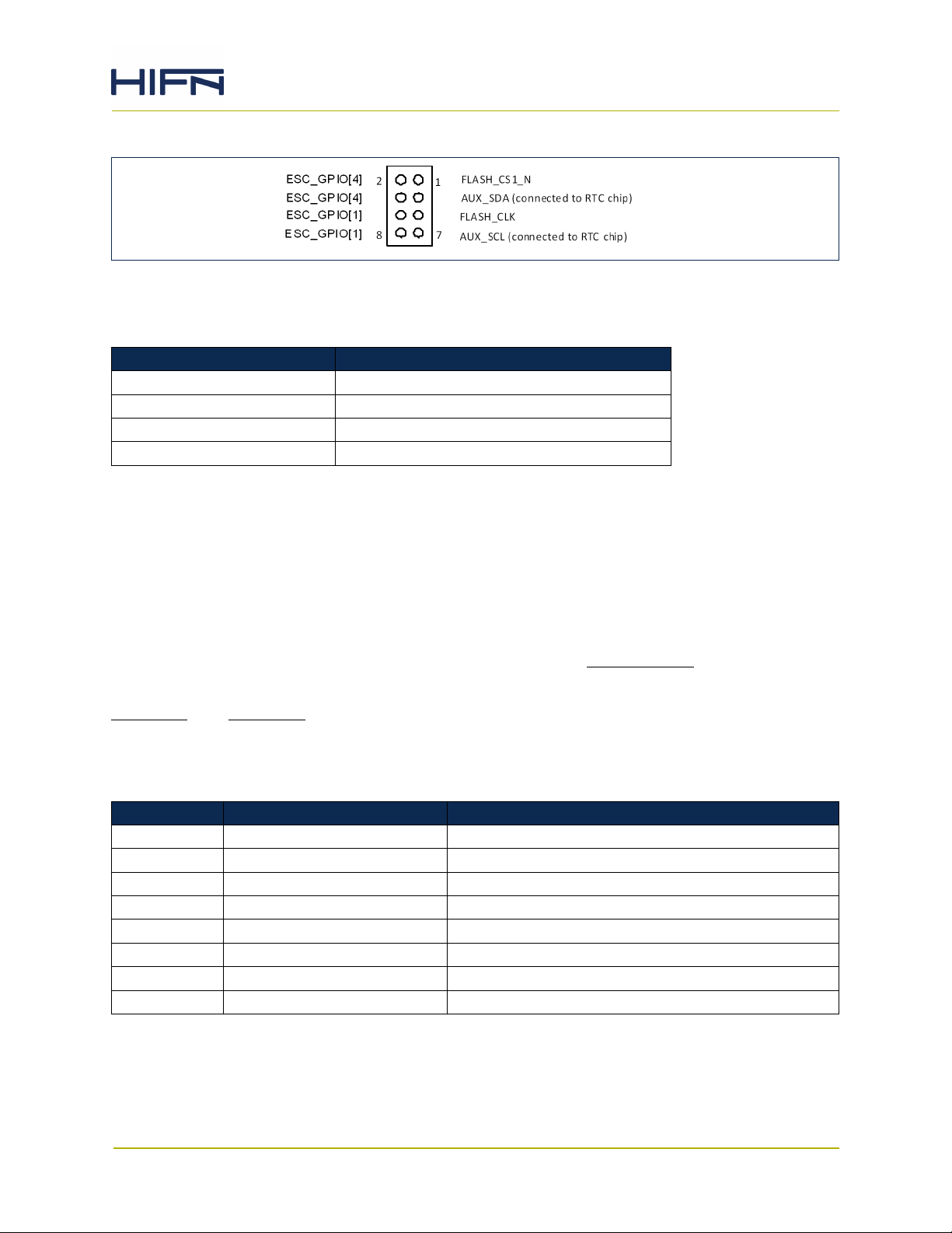
Figure 4-7. JP41 Flash/RTC Select Header Diagram
Table 4-5. JP41 Flash/RTC Select Header
Pin Number Description
1-2 ESC_GPIO[4] is used as FLASH_CS1_N
3-4 ESC_GPIO[4] is used as AUX_SDA
5-6 ESC_GPIO[1] is used as FLASH_CLK
7-8 ESC_GPIO[1] is used as AUX_SCL
4.2 LEDs
4.2.1 Communications Status LEDs
There are two LED's assigned to each of the 4 Gigabit Ethernet ports to display Link and
Activity Status. These LEDs are driven by the on-card CPLD which includes an internal mux
that allows the LEDs to be controlled by either the on-card PHY devices (default) or
optionally by the 915x device via GPIO pins. Jumper JP42 (Section 4.1.4) enables this
selection.
Table 4-6 and Table 4-7 define the behavioral differences when the LEDs are controlled by
the PHY versus the 915x for a Marvell or a Vitesse PHY.
Table 4-6. PHY-Driven Communications LEDs
LED PHY Pin Description
U63 (Marvell): LED_TX Net-1 Transmit Activity
U47 (Marvell): LINK1000 Net-1 Link (1G)
U66 (Marvell): LED_TX Host-1 Transmit Activity
U73 (Marvell): LINK1000 Host-1 Link (1G)
U43 (Vitesse): LED_1 Net-0 Link10/100/Activity
U60 (Vitesse): LED_0 Net-0 Link1000/Activity
U61 (Vitesse): LED_1 Host-0 Link10/100/Activity
U62 (Vitesse): LED_0 Host-0 Link1000/Activity
9150, 9155 Evaluation Card User Guide, UG-0210-00 Page 32
Hifn Confidential
Page 33
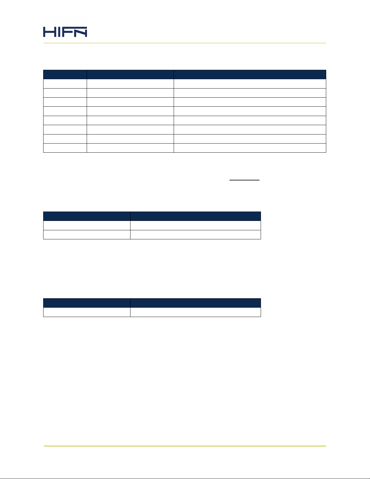
Table 4-7. 915x-Driven Communications LEDs
LED 915x Pin Description
U63 DPU_GPIO[9] Net-1 Activity
U47 DPU_GPIO[11] Net-1 Link
U66 DPU_GPIO[13] Host-1 Activity
U73 DPU_GPIO[15] Host-1 Link
U43 DPU_GPIO[8] Net-0 Activity
U60 DPU_GPIO[10] Net-0 Link
U61 DPU_GPIO[12] Host-0 Activity
U62 DPU_GPIO[14] Host-0 Link
The RMII AP Access Port is configured with a Micrel PHY device, which also provides
multiple LED output options. These LEDs are integrated into the connector. In order to
maintain similarity with the Triton card, the assignments in Table 4-8 are made on the
915x card.
Table 4-8. LEDs for RMII AC Access Port
Micrel PHY Pin Description
LED_1 Speed
LED_0 Link Activity
4.2.2 Card Status LED
A single LED will illuminate whenever power (+3.3V) is applied to the card.
Table 4-9. Card Status LED
LED Description
U12 (PWR) The 3.3V power supply is on
4.2.3 915x Status LEDs
Two LED's provide visual indication of the state of 915x's DPU and eSC processors and
firmware. The state of these LED's is undefined when the GPIO outputs are being used for
PC Mode (Hifn Use Only).
9150, 9155 Evaluation Card User Guide, UG-0210-00 Page 33
Hifn Confidential
Page 34
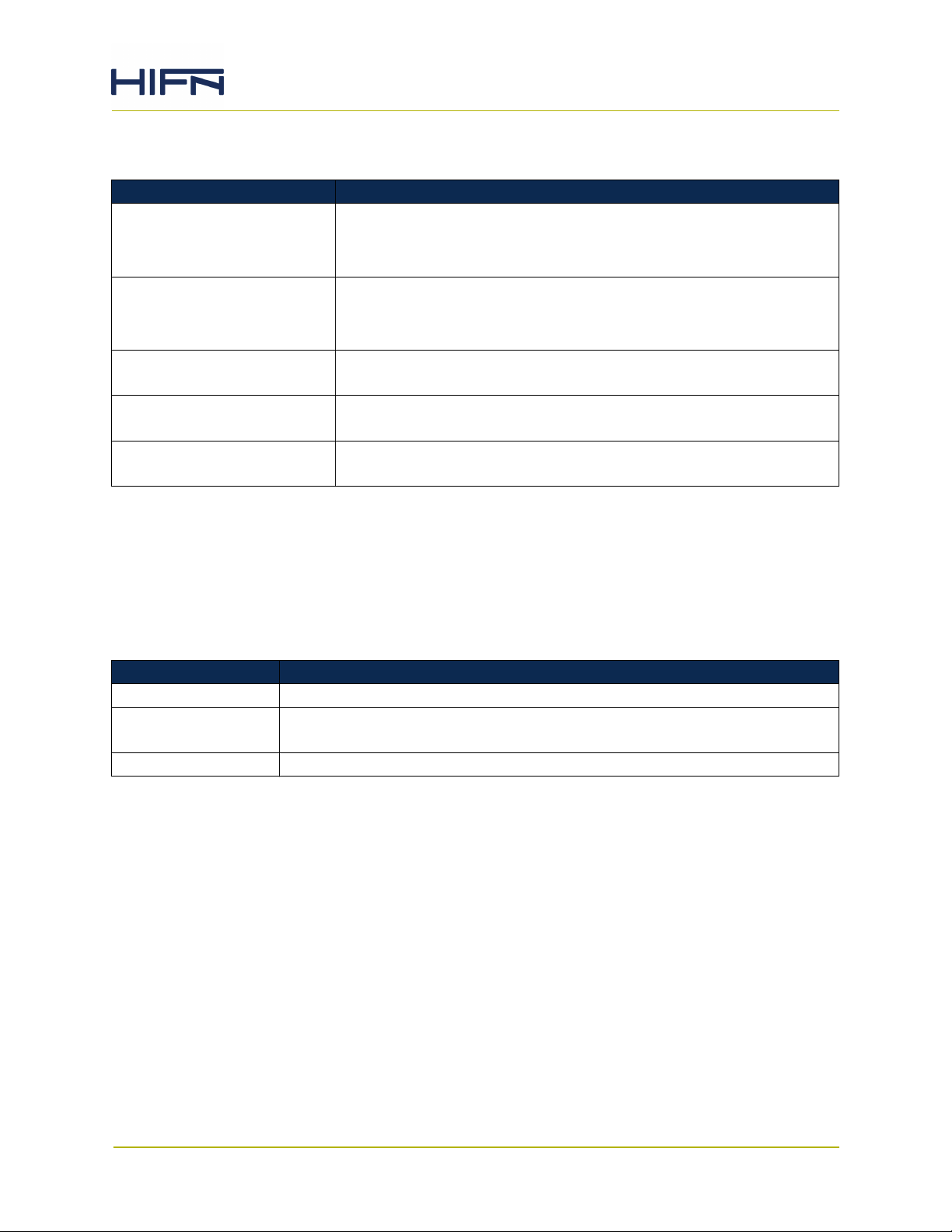
Table 4-10. 915x Status LED
LED Description
U6 (DPU) DPU Status
Connected to DPU_GPIO7, this LED may be illuminated following
power on; after DPU firmware has been loaded successfully this
LED will blink.
U24 (ESC) ESC Status
Connected to eSC_GPIO7, this LED may be illuminated following
power on; after eSC firmware has been loaded successfully this
LED will blink
U15 (SEC) Secure Mode
Hifn Use Only
U88 (TAMP) Tamper Event
Hifn Use Only
U91 (OTP) OTP Active
Hifn Use Only
4.3 Switches
There are two push-button switches for resetting various sections of the evaluation card.
The following table describes the two switches and their functionality:
Table 4-11. Switches
Switch Description
SW1 (TMPR) Hifn Use Only
SW2 (BR RST) Card Reset
When depressed, resets all on-card logic including PHY and 915x devices.
SW3 (RSVD) Hifn Use Only
9150, 9155 Evaluation Card User Guide, UG-0210-00 Page 34
Hifn Confidential
Page 35

5 Operation
As delivered from the factory, the 915x Evaluation Card includes a software kit that will
provide a mechanism for downloading code into the 915x security processor, as well as
code to initialize and configure the PHY chips on the card. After initializing the PHYs to allow
communications with the host, the firmware performs a run-time code download from the
host system.
Once the card successfully boots, the LED U6 (DPU) will illuminate to indicate that the 915x
processor is running. If this LED does not illuminate, it suggests that there is a fault with
the card power connections, jumper settings or something wrong with the card itself.
Once the run-time code is downloaded into the 915x device, the default state of the U6 LED
is a 200ms blinking rate. (Note that this the opposite of the normal default state of steadyon. The evaluation card sets a flag to the run-time code to override the default). In any
case, one of the configuration data block parameters (also known as DPU Options) can
select the LED behavior - blinking or steady on.
Refer to the 915x SDK for the necessary software tools to bootload, configure and operate
the device.
5.1 PHY Configuration
The Marvell and Vitesse Gigabit PHY devices and the Micrel RMII PHY device contain
extensive registers for control and status of the on-card Ethernet ports. These Ethernet
ports are configured through MDIO operations between the Hifn security processor and the
PHY devices. The RMII Ethernet port is also configured through MDIO operations between
the Hifn security processor and the 100 Mbps PHY. Some of the significant register
assignments that are set with the evaluation card Flash memory are listed in the following
sections.
5.1.1 SFP Ports (Host-0 and Net-0)
• Speed: 1000 Mbps
• Duplex: Full
• Pause Frames: Enable
• Port: SerDes (connects to SFP's)
5.1.2 MDI Ports (Host-1 and Net-1)
• Speed: 1000 Mbps
• Duplex: Full
• Pause Frames: Enable
• Port: Copper
9150, 9155 Evaluation Card User Guide, UG-0210-00 Page 35
Hifn Confidential
Page 36

5.1.3 MII Port
• Speed: 100 Mbps forced
• Duplex: Half
• Pause Frames: N/A
9150, 9155 Evaluation Card User Guide, UG-0210-00 Page 36
Hifn Confidential
Page 37
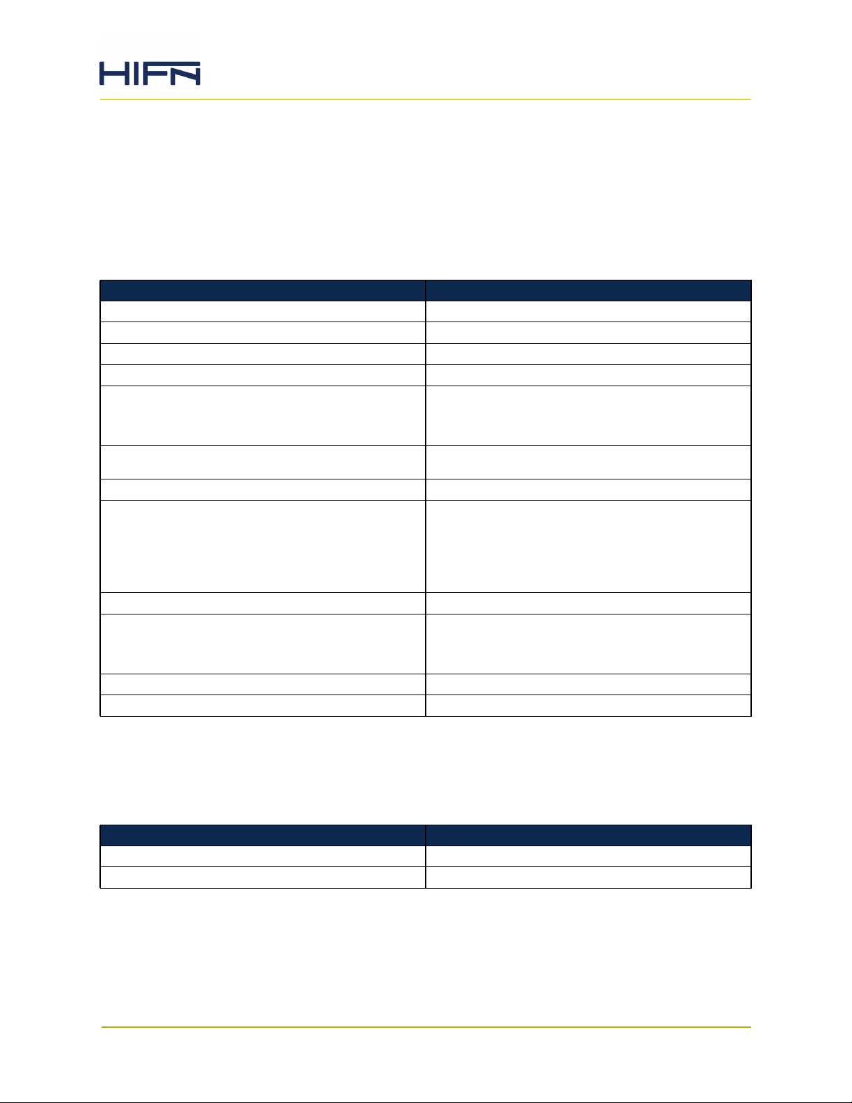
6 Specifications
6.1 General
Table 6-1. Evaluation Card Specifications
Specification Description
Dimensions 4.2" (10.7cm) x 11.15" (28.3cm)
Max component-side height 0.57" (14.5mm)
Max solder-side height 0.105" (2.7mm)
Host Interface Via Ethernet connections (No PCI bus)
Number of Gigabit Ports:
Host Ports
Network Ports
100Base-T Ports 1 (RJ45, Limited Functionality - for host
DDR2 SDRAM memory 256 Mbytes
Flash Memory
Primary Flash - AT45DB642D
Secondary Flash - AT25DF321
Note: The AT25DF321 is no longer
supported.
Card Clock Frequency 25 MHz
Hifn Device Frequency
9150
9155
SDRAM Clock Frequency 200 MHz (DDR400)
Maximum Power Consumption 15 Watts (+5V/+3.3V Combined)
2
2
control)
8 Mbytes
4 MBytes
200 MHz
250 MHz
6.2 Environmental
Table 6-2. Environmental Specifications
Specification Description
Temperature (operating) 0°C to 50°C
Temperature (storage) -20°C to 75°C
9150, 9155 Evaluation Card User Guide, UG-0210-00 Page 37
Hifn Confidential
Page 38

I Document Changes/Revisions
Documentation Changes include additions, deletions, and modifications made to this
document. This section identifies the changes made in each release of the document.
I.1 Document Revision 00
Initial release.
9150, 9155 Evaluation Card User Guide, UG-0210-00 Page 38
Hifn Confidential
Page 39

48720 Kato Road
Fremont, CA 94538
tel: 510.668.7000
www.hifn.com
Hifn Confidential
 Loading...