

Page 1

15370 Barranca Parkway
Irvine, CA 92618
iCLASS OEM75
INTEGRATION GUIDE
3141-907, Rev. B.0
January 2014
HID GLOBAL CONFIDENTIAL AND/OR PROPRIETARY INFORMATION. This document contains confidential and/or
proprietary information, which may not be duplicated, published, disseminated or disclosed, or used for any purpose,
without the written consent of HID Global Corporation. If you are an unintended recipient of this information or are
unwilling to accept the above restrictions, please immediately return this document to HID Global Corporation, 15370
Barranca Pkwy, Irvine, CA 92618-3106.
Page 2

iCLASS OEM75 Integration Guide, 3141-907, Rev. B.0
Contents
1 Overview ................................................................................................................................... 5
1.1 Introduction ........................................................................................................................................ 5
1.2 References ........................................................................................................................................ 5
1.3 Ordering ............................................................................................................................................. 5
2 Getting Started ......................................................................................................................... 6
2.1 Theory of Operation ........................................................................................................................... 6
2.2 Peripheral Circuits ............................................................................................................................. 7
2.2.1 External Noise Filter ...............................................................................................................................7
2.2.2 Adding External LEDs or Beeper ............................................................................................................7
2.2.3 Adding External Resistors ......................................................................................................................7
2.3 Transitioning from HID’s OEM50 or eProx Lock modules .................................................................. 7
2.3.1 OEM50 ...................................................................................................................................................8
2.3.2 eProx Lock Module .................................................................................................................................8
3 Software Integration Recommendations ............................................................................... 9
4 Mechanical Specifications .................................................................................................... 11
4.1 OEM75 Module – 3141Axx .............................................................................................................. 12
4.2 OEM75 Module – 3141ADx ............................................................................................................. 13
4.3 Antennas ......................................................................................................................................... 14
4.3.1 Antenna Model 3142 ............................................................................................................................ 15
4.3.2 Antenna Model 3144 ............................................................................................................................ 15
4.3.3 Antenna Model 3146 ............................................................................................................................ 16
4.3.4 Antenna Model 3148 ............................................................................................................................ 16
4.3.5 Antenna Model 3153 ............................................................................................................................ 17
4.4 Antenna Interfacing.......................................................................................................................... 17
5 Electrical Specifications ........................................................................................................ 18
5.1 Power Supply .................................................................................................................................. 18
5.2 Electrical Connections ..................................................................................................................... 18
5.3 I/O Specifications ............................................................................................................................. 20
5.4 P1 connector Ping Mode Static States ............................................................................................ 22
5.5 Electrical Application Hints .............................................................................................................. 22
6 Firmware ................................................................................................................................. 23
6.1 Applications ..................................................................................................................................... 23
6.2 Feature Bundles and Configuration ................................................................................................. 23
6.3 Updates ........................................................................................................................................... 23
6.4 Communication ................................................................................................................................ 23
6.5 SPI Implementation ......................................................................................................................... 23
6.6 General Recommendations ............................................................................................................. 24
6.7 SPI Message Transmission ............................................................................................................. 27
6.7.1 Host SPI Master Write Function ........................................................................................................... 27
6.7.2 Host SPI Master Read Function ........................................................................................................... 27
6.7.3 Peripheral Processor SPI Slave Interrupt Processing ........................................................................... 27
6.7.4 Sample Source Code ........................................................................................................................... 28
6.8 I²C Implementation .......................................................................................................................... 32
6.8.1 General Recommendations .................................................................................................................. 32
6.8.2 I²C Baud Rates and Clock Stretching ................................................................................................... 32
6.8.3 I²C Message Transmission ................................................................................................................... 32
Page 2 of 49 January 2014
6.8.4 Sample Source Code - I²C ................................................................................................................... 34
HID GLOBAL CONFIDENTIAL AND/OR PROPRIETARY INFORMATION. This document contains confidential and/or proprietary
information, which may not be duplicated, published, disseminated or disclosed, or used for any purpose, without the written
consent of HID Global Corporation. If you are an unintended recipient of this information or are unwilling to accept the above
restrictions, please immediately return this document to HID Global Corporation, 15370 Barranca Pkwy, Irvine, CA 92618-3106.
Page 3

iCLASS OEM75 Integration Guide, 3141-907, Rev. B.0
6.8.5 Wiegand ............................................................................................................................................... 43
6.8.6 Serial .................................................................................................................................................... 43
6.8.7 Timing .................................................................................................................................................. 44
7 OEM75 Module Configuration ............................................................................................... 45
7.1 Configuration Options ...................................................................................................................... 45
7.2 Configuration Card Availability ......................................................................................................... 45
7.3 Custom Configurations for High Volume Manufacturing Availability ................................................ 45
7.4 Reconfiguring the OEM75 in Normal Power Mode .......................................................................... 45
7.5 Reconfiguring the OEM75 in Ultra Low Power Mode....................................................................... 45
7.6 Regulatory ....................................................................................................................................... 47
8 Additional Tools ..................................................................................................................... 48
January 2014 Page 3 of 49
HID GLOBAL CONFIDENTIAL AND/OR PROPRIETARY INFORMATION. This document contains confidential and/or proprietary
information, which may not be duplicated, published, disseminated or disclosed, or used for any purpose, without the written
consent of HID Global Corporation. If you are an unintended recipient of this information or are unwilling to accept the above
restrictions, please immediately return this document to HID Global Corporation, 15370 Barranca Pkwy, Irvine, CA 92618-3106.
Page 4

03/2011
First Release
A.0
Fax: 949 732 2120
Phoenix Road
Fax: 852 3160 4809
Copyright
© 2010-2014 HID Global Corporation/ASSA ABLOY AB. All rights reserved.
Trademarks
HID GLOBAL, HID, the HID logo, iCLASS, OEM 75, and eProx are the trademarks or registered
trademarks of HID Global Corporation, or its licensors, in the U.S. and other countries.
MIFARE is a registered trademarks of NXP B.V. and are used under license.
Disclaimer
This guide presents suggestions for proper usage and integration. Good Mechanical and
Electrical Engineering practices are required to insure a quality final product.
Revision History
Date Description Version
01/14/2014 Update Module Dimensions B.0
iCLASS OEM75 Integration Guide, 3141-907, Rev. B.0
Contacts
North America
15370 Barranca Parkway
Irvine, CA 92618
USA
Phone: 800 237 7769
Europe, Middle East and Africa
Haverhill, Suffolk CB9 7AE
England
Phone: +44 1440 714 850
Fax: +44 1440 714 840
Asia Pacific
19/F 625 King’s Road
North Point, Island East
Hong Kong
Phone: 852 3160 9800
support.hidglobal.com
Page 4 of 49 January 2014
HID GLOBAL CONFIDENTIAL AND/OR PROPRIETARY INFORMATION. This document contains confidential and/or proprietary
information, which may not be duplicated, published, disseminated or disclosed, or used for any purpose, without the written
consent of HID Global Corporation. If you are an unintended recipient of this information or are unwilling to accept the above
restrictions, please immediately return this document to HID Global Corporation, 15370 Barranca Pkwy, Irvine, CA 92618-3106.
Page 5

iCLASS OEM75 Integration Guide, 3141-907, Rev. B.0
HID
3141-901
OEM75 User Manual
1 Overview
1.1 Introduction
The OEM75® is designed to offer iCLASS® and MIFARE® technology to a wide variety of service
providers using applications such as vending machines, biometric readers, card printers, time and
attendance terminals, and alarm panels and more. The OEM75 is a third generation iCLASS
module, offers ultra-low power consumption (configuration dependent), on-board voltage regulation,
versatile ISO polling configuration, and various data outputs to enable a variety of hardware
communication protocols. The UART, SPI, I2C and Wiegand communications allow for an OEM to
have the power of iCLASS at their fingertips.
The OEM75 is designed to be a component in an upper level assembly and can operate with one of
several antenna sizes. This Integration Guide provides recommendations which improve the
integrator’s experience. This guide addresses Electrical, Mechanical, Software Interface and
Antenna integration issues.
1.2 References
Source Part Number Description
HID 1356_MHz HTOG How to Order Guide (HTOG)
http://www.hidcorp.com > documents > 13.56 MHz How to
Order Guide
Security Industry
Association
HID 3141-905 OEM75 Interface Protocol
SIA AC-01 (1996.10) Wiegand Card Reader Interface Standard
1.3 Ordering
See the iCLASS OEM75 User Manual for ordering considerations. This document assumes that
OEM75 hardware and the Development Kit are in the user’s possession.
January 2014 Page 5 of 49
HID GLOBAL CONFIDENTIAL AND/OR PROPRIETARY INFORMATION. This document contains confidential and/or proprietary
information, which may not be duplicated, published, disseminated or disclosed, or used for any purpose, without the written
consent of HID Global Corporation. If you are an unintended recipient of this information or are unwilling to accept the above
restrictions, please immediately return this document to HID Global Corporation, 15370 Barranca Pkwy, Irvine, CA 92618-3106.
Page 6

Ultra Low Power
OEM75 Module
OEM75
Antenna
iCLASS
Card
/RESET
/HOLD
/GREEN_LED_
CARD_PRESENT
Host Hardware/Application
Wiegand Data 0
Wiegand Data 1
/BEEPER
/RED_LED
UART RX
UART TX
I
2
C SCLK / SPI_ CLK
SPI_CS
SPI_MISO
I
2
C CSDA / SPI_MOSI
4
4
5
2 Getting Started
2.1 Theory of Operation
Configurable operation modes include:
• Autonomous – In this mode, the module polls for a card constantly and will not accept
serial commands unless a card is in the field. Autonomous is the default operation of the
OEM75.
• API – The module acts the same as in Autonomous operation except the module is always
ready to receive a command from the host. When an RF or Serial command is received,
the module will wait a configurable amount of time before it returns to polling for a card.
iCLASS OEM75 Integration Guide, 3141-907, Rev. B.0
Page 6 of 49 January 2014
HID GLOBAL CONFIDENTIAL AND/OR PROPRIETARY INFORMATION. This document contains confidential and/or proprietary
information, which may not be duplicated, published, disseminated or disclosed, or used for any purpose, without the written
consent of HID Global Corporation. If you are an unintended recipient of this information or are unwilling to accept the above
restrictions, please immediately return this document to HID Global Corporation, 15370 Barranca Pkwy, Irvine, CA 92618-3106.
Figure 2-1: OEM75 Operation
Power Modes Include:
• Ultra Low Power – The module is in Ultra Low Power mode as it polls for a card. When a
card is detected in the RF field, the module wakes up, reads the card data, changes the
Card Present line, outputs the card data, and goes back to sleep within a configured period
of time to conserve power. Use this mode with battery power.
• Standard – The module is constantly powered on and polling for cards. The module is
never asleep in this mode. Use this mode with an external power supply.
Power Autonomous Mode Remote Mode Autonomous Remote Mode
Standard Power
Page 7

iCLASS OEM75 Integration Guide, 3141-907, Rev. B.0
2.2 Peripheral Circuits
The following section details recommended peripheral circuitry.
2.2.1 External Noise Filter
If false card detections occur in Ultra Low Power Mode, or the host has spectral noise, a line filter
designed to block frequencies in the 10 KHz to 50 KHz range is beneficial when inlined with the
power line.
2.2.2 Adding External LEDs or Beeper
Connect external LEDs to the OEM75 by connecting wires to the P2 connector The LEDs are
connected to an external +3.3VDC supply with an external series current limit resistor.
See Table 5-5: P2 I/O Electrical Specifications.
The Cathodes are connected through an external resistor to the RED or GREEN LED connector
port signals. The OEM supplies current limiting resistors for modules.
The value of these resistors will depend on how much current is provided for the LEDs. The
combined voltage drop of the resistor and output low voltage of the OEM75 on these signal lines
should be factored in when selecting the LED brightness.
2.2.3 Adding External Resistors
For I2C Mode operation, external 10k pull-up resistors are required on the SCLK signals.
Note: There is already an internal pull-up resistor on the I2C SDA signal.
2.3 Transitioning from HID’s OEM50 or eProx Lock modules
Provided are suggestions for transitioning from the HID OEM50 and HID eProx Lock modules to the
OEM75.
January 2014 Page 7 of 49
HID GLOBAL CONFIDENTIAL AND/OR PROPRIETARY INFORMATION. This document contains confidential and/or proprietary
information, which may not be duplicated, published, disseminated or disclosed, or used for any purpose, without the written
consent of HID Global Corporation. If you are an unintended recipient of this information or are unwilling to accept the above
restrictions, please immediately return this document to HID Global Corporation, 15370 Barranca Pkwy, Irvine, CA 92618-3106.
Page 8

P2 Connector
Pin 1
Exc Supply
No signal on the OEM75
Pin 3
Serial Transmit
Same as OEM75 P1 pin 8 - UART Transmit
Pin 4
Serial Receive
Same as OEM75 P1 pin 7 - UART Receive
and 5VDC is a good supply voltage
P1 Connector
Pin 1
Open Output
OEM75 does not have a similar signal
Pin 2
Ground
Same as OEM75 P1 pin 2, signal Ground
OEM50 is inverted logic
2.3.1 OEM50
If transitioning from an OEM50 – here are the differences.
The OEM50 connector is a 2 X 6 0.1" space pin header or PWB hole pattern.
The OEM50 has a two-wire interface to the antenna and the OEM75 has a four-wire interface.
Therefore, the OEM50 antenna will not work with the OEM75, and vice versa.
The harness and signal changes to adapt the signals from the OEM50 2 X 6 pattern to an
OEM75 1 x 9 1.25mm pattern are the following.
Note: The additional P2 for HSI and SPI interfaces are 1 x 8 1.25mm pattern.
OEM50 OEM75
iCLASS OEM75 Integration Guide, 3141-907, Rev. B.0
Pin 2
Exc Return is not
used
Pin 5 Vdd Return Same as OEM75 P2 pin 2 - Battery Minus
Pin 6 Vdd +5VDC
Pin 3 Wiegand Data1
Pin 4 Wiegand Data0
2.3.2 eProx Lock Module
The eProx® Lock connector is mechanically the same as the OEM75’s connector P2. Be aware
however, that the connections between the OEM75 module and the eProx Lock module are
reversed. This implies that a straight-thru cable will not work. A 180 degree twist of the cable is
required to insure that Pin 1 on one of the modules correctly mates with Pin 1 on the other module.
No signal on the OEM75
Same as OEM75 P2 pin 1 - Battery Positive
Wiegand data output is per the SIA AC-01 (1996.10)
specification, except Voh is 3.3VDC max, and not 4.0
to 5.5 VDC
Wiegand data output is per the SIA AC-01 (1996.10)
specification, except Voh is 3.3VDC max, and not 4.0
to 5.5 VDC
OEM50 is inverted logic
The two-wire 125 kHz antenna for the eProx Lock is not interchangeable with an OEM75 antenna.
Page 8 of 49 January 2014
HID GLOBAL CONFIDENTIAL AND/OR PROPRIETARY INFORMATION. This document contains confidential and/or proprietary
information, which may not be duplicated, published, disseminated or disclosed, or used for any purpose, without the written
consent of HID Global Corporation. If you are an unintended recipient of this information or are unwilling to accept the above
restrictions, please immediately return this document to HID Global Corporation, 15370 Barranca Pkwy, Irvine, CA 92618-3106.
Page 9
iCLASS OEM75 Integration Guide, 3141-907, Rev. B.0
3 Software Integration Recommendations
The following section details recommended software operational interfacing. The reader of this
guide should use this information in conjunction with the OEM75 Interface Protocol Manual.
Previously it has been shown how the OEM75 reader module interacts with the processor in the
OEM75 Development Kit.
This discourse applies to a Host based application communicating/controlling/querying the OEM75
based reader firmware. The explanation of the operation is independent of type of hardware used to
communicate with the OEM75. This information applies whether a UART, SPI or I2C serial
connection is used. A user application must first update the data structure Application Protocol Data
Unit APDB
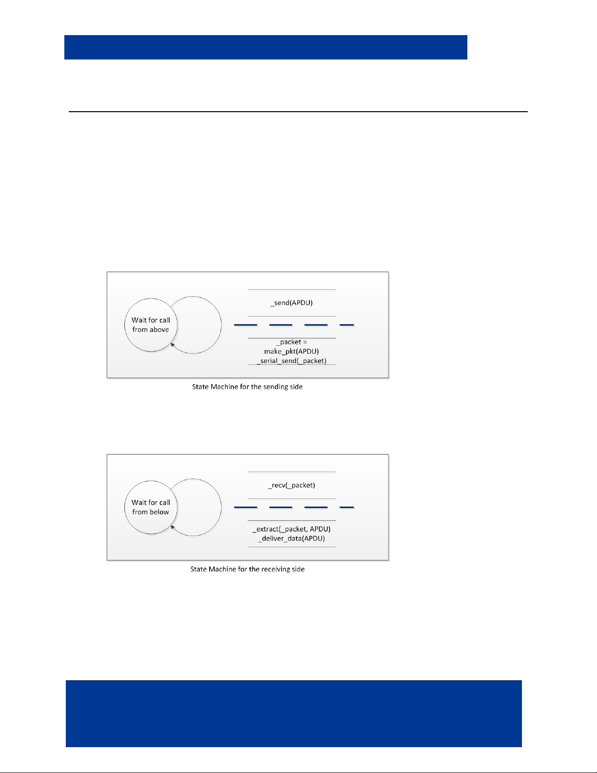
Consider initially the transmission of a command to the OEM75 from a host. The state machine
representation indicates the state of the task, the event that transitions the task is indicated above
the dotted line and the action taken is indicated below the dotted line in the figure below.
When the host application has properly initialized an APDU, it raises the event _send(APDU). This
event triggers a call to make_pkt(APDU) which encapsulates the control block into a serial packet
and then calls _serial_send(_packet) which places the _packet on the serial output lines. The state
machine then reverts back to a “Wait for call from above” state.
When the OEM75 recognizes the receipt of a packet by means of the event _recv(_packet), it
makes a call to _extract(_packet, APDU) in order to extract the APDU from the packet and then call
_deliver_data(APDU) which passes the APDU up to the higher layers for evaluation. The state
machine returns to a state of “Wait for call from below”.
The above state machines represent the transmission of a command from the host to the reader at
its most simplistic level. The operations also assume a perfect world in which no transmission line
bit corruption occurs. In actuality the state machines must be a bit more complicated than initially
January 2014 Page 9 of 49
HID GLOBAL CONFIDENTIAL AND/OR PROPRIETARY INFORMATION. This document contains confidential and/or proprietary
information, which may not be duplicated, published, disseminated or disclosed, or used for any purpose, without the written
consent of HID Global Corporation. If you are an unintended recipient of this information or are unwilling to accept the above
restrictions, please immediately return this document to HID Global Corporation, 15370 Barranca Pkwy, Irvine, CA 92618-3106.
Page 10

iCLASS OEM75 Integration Guide, 3141-907, Rev. B.0
presented in order to recover from potential errors. It must be kept in mind that a similar set of state
machines apply to the communication from the OEM75 to the host computer. The protocol
operating in the OEM75 expects the delay between the stop bit of the preceding byte and the start
bit of the next byte to be less than 500 milliseconds. This implies that a complete APDU is
transmitted.
Let us now take into account the potential of sending the packet over an extended distance. Let us
assume a maximum packet size of 263 bytes. For the most basic UART transmission at 57.6 Kbps
with 2 stop bits and even parity. The recommended length of cable for proper operation is no longer
than 50 feet and smaller lengths are specified for higher speed connections. The speed of an
electrical signal is approximately 3 nsecs. per foot. A signal change on one end of the cable will be
recognized approximately 3 nsecs/ft. *50 ft = 150 nsecs later on the other end of the cable. The bit
time, that is the time to generate a bit is 1.0 / 57.6 Kbps = 17.36 microseconds per bit. Since this
time is much greater than the transmission time of any change we can effectively ignore the transit
time or the time it takes an electron to move from the source side to the destination side. The time it
takes to transmit an entire byte including the start, stop and parity bits is then just 12 * 17.36
microseconds = 208 microseconds per byte. The time it takes to transmit a maximum length APDU
is 208 * 263 = 54.79 milliseconds. The time to transmit back a 2 byte status is 416 microseconds, or
0.000416 milliseconds. If we assume no processing delays in the OEM75 the time from
transmission to complete reception of an acknowledgement is then 55.206 milliseconds. The above
analysis indicates that any timeout value used must be at least this large independent of the time it
takes to process a command. The time it takes to execute each of the commands is command
dependent.
This protocol cannot recover from multiple bit errors. A single bit error per byte can be detected, in
which case either the host or the reader should ignore the entire message. A timeout should occur
and the communication can be re-initiated. It is possible for an APDU to be corrupted when
transmitting it to the OEM75 if the unit is connected to the host by means of a very long cable and
that cable is routed near sources of electromagnetic interference. It is possible with the above
conditions that bit corruption modifies the command field of an APDU resulting in an invalid
execution. It is not recommended that the OEM75 be operated in this manner. In the scenarios
depicted in section 2 of this document, the serial cable had a length of 6 feet.
Ultra-Low power applications must create a host interface which recognizes the CP (Card Present)
signal generated by the constantly energized processor receiving antenna signals. This signal has a
dual purpose, it is used not only to indicate a Card Present Event to the Host Processor but it also
wakes up the OEM75 main processor. The host interface must keep in mind that the OEM75 main
processor requires some time to power up and initialize before it can respond to either card or host
requests. It is recommended that the CP signal be used as an interrupt signal to the Host
processor. The Host processor should respond to this interrupt by setting a flag indicating that the
CP event has been recognized and then return to the main processing task which should use the
flag as an indication that Card Data needs to be read from the OEM75. The Host Application should
delay a set period of time allowing the OEM75 main processor time to wake-up and initialize itself.
After this time period the Host can request the card information.
Page 10 of 49 January 2014
HID GLOBAL CONFIDENTIAL AND/OR PROPRIETARY INFORMATION. This document contains confidential and/or proprietary
information, which may not be duplicated, published, disseminated or disclosed, or used for any purpose, without the written
consent of HID Global Corporation. If you are an unintended recipient of this information or are unwilling to accept the above
restrictions, please immediately return this document to HID Global Corporation, 15370 Barranca Pkwy, Irvine, CA 92618-3106.
Page 11

iCLASS OEM75 Integration Guide, 3141-907, Rev. B.0
4 Mechanical Specifications
The following section details all mechanical specifications for the OEM75 module, antennas and
interfaces.
The connectors recommended are:
• P1 – An 8-position pin socket header.
Molex Part Number: 53048-0810
Tyco Part Number: 1734829-8
• P2 – A 9-position pin socket header
Molex Part Number: 53048-0910
Tyco Part Number: 1734829-9
• P3 – A 4 Pin right-angle zero-insertion-force connector.
Molex Part Number: 39-53-2044
Note: On OEM 75 part number 3141AD models the form-factor of the circuit board is so small as to
prohibit the use of Molex Part Number: 39-53-2044 on the board. You should investigate other
methods of connecting to an antenna.
The following are the recommend cables that should be used with the OEM 75 modules.
The cable connecting P3 to the antenna connection is called JUDD wire. It is manufactured by both
Judd Corporation and Sumitomo Corporation. This cable is somewhat brittle and the repeated
bending of the cable should be avoided to minimize breakage. User implementations should strive
to limit the length of this interconnection cable.
P1 is an 8-pin connector socket which accepts an 8-pin connector plug MOLEX Part Number:
51021-0800. The wire used is an AWG #28, 8 conductor flat cable
P2 is a 9-pin connector socket which accepts a 9-pin connector plug MOLEX Part Number:
51021-0900. The wire used is an AWG #28, 9 conductor flat cable
Antenna and module form factor specifications are discussed within this section.
January 2014 Page 11 of 49
HID GLOBAL CONFIDENTIAL AND/OR PROPRIETARY INFORMATION. This document contains confidential and/or proprietary
information, which may not be duplicated, published, disseminated or disclosed, or used for any purpose, without the written
consent of HID Global Corporation. If you are an unintended recipient of this information or are unwilling to accept the above
restrictions, please immediately return this document to HID Global Corporation, 15370 Barranca Pkwy, Irvine, CA 92618-3106.
Page 12

Angular
±1º Bend
±1º
.XX
±.01 [.3]
Note: In the following mechanical drawings, unless otherwise specified the dimensions are in
inches and [millimeters]. Tolerances are as follows:
Tolerances Definition
.XXX ±.005 [.13]
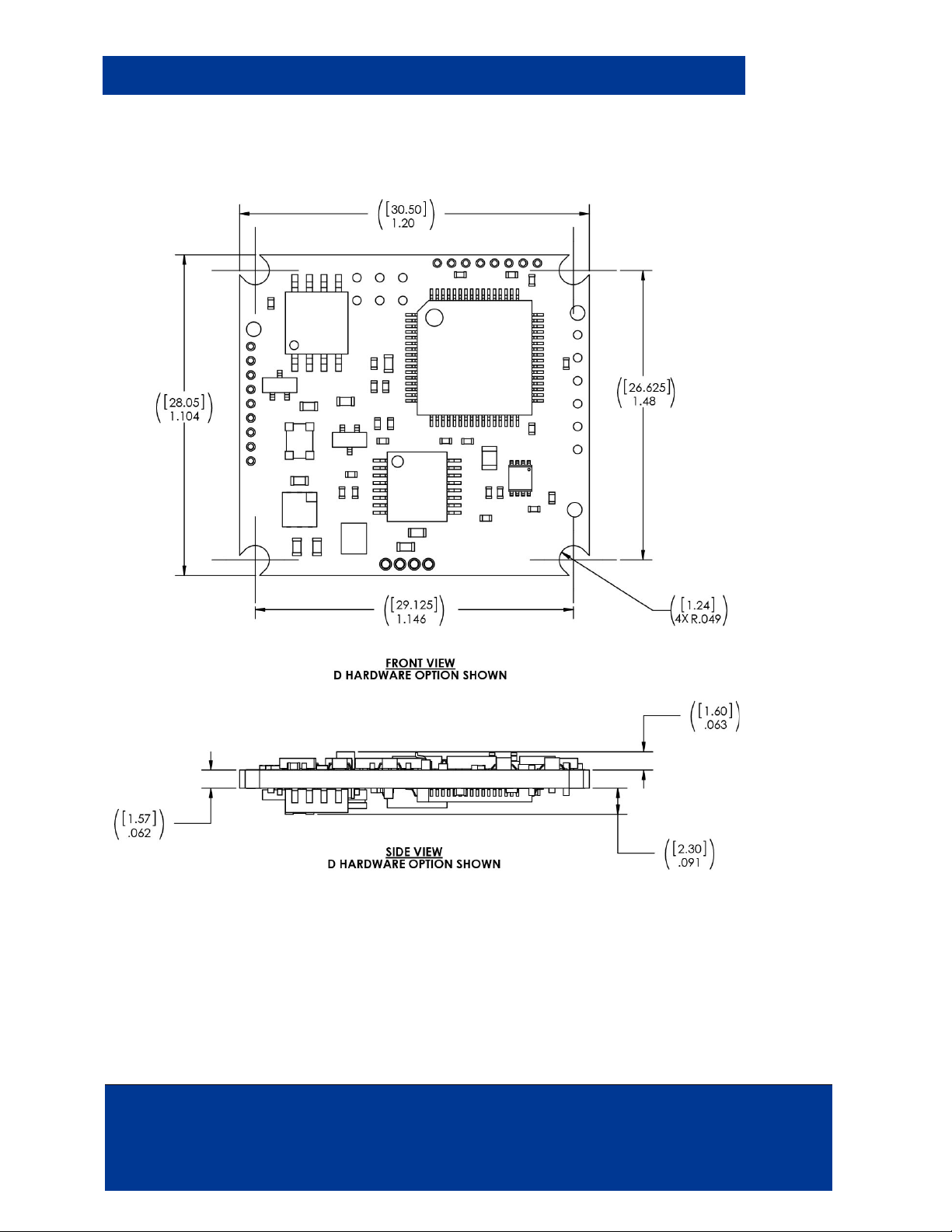
4.1 OEM75 Module – 3141Axx
iCLASS OEM75 Integration Guide, 3141-907, Rev. B.0
Figure 4-1: OEM75 – 3141Axx
Note: The 20mil P1, P2 and P3 holes can accept 26 AWG (0.41 mm, 0.13 mm
mm, 0.08 mm
Page 12 of 49 January 2014
HID GLOBAL CONFIDENTIAL AND/OR PROPRIETARY INFORMATION. This document contains confidential and/or proprietary
information, which may not be duplicated, published, disseminated or disclosed, or used for any purpose, without the written
consent of HID Global Corporation. If you are an unintended recipient of this information or are unwilling to accept the above
restrictions, please immediately return this document to HID Global Corporation, 15370 Barranca Pkwy, Irvine, CA 92618-3106.
2
) wires.
2
) or 28 AWG (0.33
Page 13
iCLASS OEM75 Integration Guide, 3141-907, Rev. B.0
4.2 OEM75 Module – 3141ADx
Figure 4-2: OEM75 – 3141ADx
The OEM75 – 3141ADx was designed to be the smallest form factor possible. This module offering
was designed to be header mounted on a host board utilizing the P1 and P2 connectors.
Note: The 20mil P1 and P2 holes can accept 26 AWG (0.41 mm, 0.13 mm
0.08 mm
2
) wires.
2
) or 28 AWG (0.33 mm,
January 2014 Page 13 of 49
HID GLOBAL CONFIDENTIAL AND/OR PROPRIETARY INFORMATION. This document contains confidential and/or proprietary
information, which may not be duplicated, published, disseminated or disclosed, or used for any purpose, without the written
consent of HID Global Corporation. If you are an unintended recipient of this information or are unwilling to accept the above
restrictions, please immediately return this document to HID Global Corporation, 15370 Barranca Pkwy, Irvine, CA 92618-3106.
Page 14

3.0 in
[78 mm]
2.3 in
[60 mm]
Read Range
1.5 in
[40 mm]
4.0 in
[101 mm]
6.0 in
[160 mm]
Cable Length
S
t
a
n
d
a
r
d
P
o
w
e
r
Ultra Low
Power Mode
2.7 in
[70 mm]
4.3 Antennas
Basic Antenna Operation
Credentials obtain their power from the magnetic field generated by the antenna of the reader. At
the operating frequency of the reader this interaction is similar to the operation of an air core
transformer. When an antenna is energized by an alternating current the induced magnetic field is
directly proportional to the area enclosed by the antenna loop. The larger the loop, the more
excitation current is required to produce the same level of magnetic flux. That flux covers a larger
area and so the read range is extended. Other external factors can affect the magnitude of this
induced magnetic field. Magnetic lines of flux when generated by a loop antenna are oriented
perpendicular to the plane of the loop. This is known as the right-hand rule, the magnetic field wraps
around the wire in the direction of current flow.
The antennas for the OEM75 are available in two different configurations.
• Non-tuned
Non-tuned antennas do not have tuning components loaded. OEM customers must stuff
parallel and series capacitance in order to custom-tune non-tuned antennas to their specific
environment. There are many factors involved with antenna tuning regarding proximity to
metal and electronics. HID Global can provide assistance with tuning antennas for custom
OEM environments. Contact your local HID Connect Technical Support for details.
• Air-tuned
Air-tuned antennas do have tuning components loaded. The antenna is pre-tuned for open
air conditions (for example, not near metal). When an air-tuned antenna is placed near
metal, its tuning is affected causing it to perform with a slightly smaller read range. More
importantly, communication errors become more frequent when large data transfers are
involved. All air-tuned antennas are pre-tuned for a 4.0 in (101 mm) cable length. For cable
lengths of differing sizes, reference the following graph for read range impacts.
iCLASS OEM75 Integration Guide, 3141-907, Rev. B.0
Figure 4-3: Power Modes and Air-tuned Antenna (3142)
Match the signal and ground connections from the antenna to the OEM75 module with a ribbon
cable (1.25mm spacing).
Due to power requirements, applications requiring PIV smart card support require a larger antenna.
The environment where the antenna is placed and tuning also affect the performance. Consult
Connect Technical Support for assistance in choosing an antenna for your environment.
Page 14 of 49 January 2014
HID GLOBAL CONFIDENTIAL AND/OR PROPRIETARY INFORMATION. This document contains confidential and/or proprietary
information, which may not be duplicated, published, disseminated or disclosed, or used for any purpose, without the written
consent of HID Global Corporation. If you are an unintended recipient of this information or are unwilling to accept the above
restrictions, please immediately return this document to HID Global Corporation, 15370 Barranca Pkwy, Irvine, CA 92618-3106.
Page 15

iCLASS OEM75 Integration Guide, 3141-907, Rev. B.0
It should be recognized that mounting the loop antenna in close proximity to a metallic ground plane
reduces the effective range of the card reader. If such a mounting is required it is recommended
that the metallic ground plane have slots cut in it to reduce the generation of eddy loop currents.
• The following diagrams provide examples of Air-tuned Antenna’s.
4.3.1 Antenna Model 3142
Figure 4-4: 3142 A16 Antenna
4.3.2 Antenna Model 3144
Figure 4-5: 3144 A9 Antenna
January 2014 Page 15 of 49
HID GLOBAL CONFIDENTIAL AND/OR PROPRIETARY INFORMATION. This document contains confidential and/or proprietary
information, which may not be duplicated, published, disseminated or disclosed, or used for any purpose, without the written
consent of HID Global Corporation. If you are an unintended recipient of this information or are unwilling to accept the above
restrictions, please immediately return this document to HID Global Corporation, 15370 Barranca Pkwy, Irvine, CA 92618-3106.
Page 16

4.3.3 Antenna Model 3146
Figure 4-6: 3146 A12 Antenna
iCLASS OEM75 Integration Guide, 3141-907, Rev. B.0
4.3.4 Antenna Model 3148
Figure 4-7: 3148 A17 Antenna
Page 16 of 49 January 2014
HID GLOBAL CONFIDENTIAL AND/OR PROPRIETARY INFORMATION. This document contains confidential and/or proprietary
information, which may not be duplicated, published, disseminated or disclosed, or used for any purpose, without the written
consent of HID Global Corporation. If you are an unintended recipient of this information or are unwilling to accept the above
restrictions, please immediately return this document to HID Global Corporation, 15370 Barranca Pkwy, Irvine, CA 92618-3106.
Page 17

iCLASS OEM75 Integration Guide, 3141-907, Rev. B.0
P1 Connector
Additional COM methods for SPI, UART or I2C functions
P2 Connector
Standard reader interfaces
P3 Connector
Four through holes labeled antenna drive, feedback, ground 1, and ground 2.
4.3.5 Antenna Model 3153
Figure 4-8: 3153 A15 Antenna
4.4 Antenna Interfacing
The following table summarizes mounting for these antennas and the associated connectors.
Use this table in conjunction with the OEM75 mechanical specifications in order to determine the
physical location of pins.
January 2014 Page 17 of 49
HID GLOBAL CONFIDENTIAL AND/OR PROPRIETARY INFORMATION. This document contains confidential and/or proprietary
information, which may not be duplicated, published, disseminated or disclosed, or used for any purpose, without the written
consent of HID Global Corporation. If you are an unintended recipient of this information or are unwilling to accept the above
restrictions, please immediately return this document to HID Global Corporation, 15370 Barranca Pkwy, Irvine, CA 92618-3106.
Page 18

Nominal
current
5 Electrical Specifications
5.1 Power Supply
The following table specifies necessary power supply specifications.
Table 5-1: I/O Electrical Specifications
Pin Name Parameters Notes
Voltage Current
iCLASS OEM75 Integration Guide, 3141-907, Rev. B.0
40mA +/- 3mA
Reader mode (no card)
Battery Positive
to
Ground
4.0 VDC
to
10.0 VDC
Note: If implementing the OEM75 in a UL listed product, UL requires voltage range tolerances
of -15% to +10%.
5.2 Electrical Connections
The OEM75 is designed for a host with 3.3 VDC or 5.0 VDC I/O interfacing. All input signals to the
OEM75 are 5 VDC tolerant. All output signals are open collector; except the Wiegand lines have a
1K pull up to a diode isolated +3.3 VDC.
For the P1 connector signals, the input interface logic levels are the following specifications for
output logic levels.
< 0.5 VDC for Vil
> 2.0 VDC for Vih
< 0.4 VDC for Vol
> 2.4 VDC for Voh
External LED’s can be added to the board by connecting the LED pins located next to the beeper
on the upper left portion of the board (see Figure 4-1 – OEM75 – 3141Axx). The LEDs can be
controlled with serial commands or using the LED control lines listed in the following table.
80mA +/- 5mA
Peak
12uA +/-3uA Ultra-Low Power Mode (no
Card reading current
card) current
CAUTION: Install a 1K Ohm serial resistor on the SPI lines in SPI communication mode to
eliminate negative voltage spikes.
Page 18 of 49 January 2014
HID GLOBAL CONFIDENTIAL AND/OR PROPRIETARY INFORMATION. This document contains confidential and/or proprietary
information, which may not be duplicated, published, disseminated or disclosed, or used for any purpose, without the written
consent of HID Global Corporation. If you are an unintended recipient of this information or are unwilling to accept the above
restrictions, please immediately return this document to HID Global Corporation, 15370 Barranca Pkwy, Irvine, CA 92618-3106.
Page 19

iCLASS OEM75 Integration Guide, 3141-907, Rev. B.0
P1 3 SPI Clock / (I2C SCLK)
Clock signal for either SPI or I2C
P1 7 UART Receive
Serial Input Line
P2 1 Supply Voltage
Positive (V+)
Input
Power Supply Positive Voltage
Negative (V-)
antenna.
P2 6 Wiegand Data 0
Output
Internal 1K to +3.3VDC & Collector
P2 7 Wiegand Data 1
Output
Internal 1K to +3.3VDC & Collector
P2 8 /Beeper
Output
Active Low signal which enables off
board signaling
enable an off board Red LED
P3 3 Ground 1
P3 4 Ground 2
Table 5-2: P1 Connector I/O Functionality
Connection Pin #` Signal Name Function
P1 1 +3.3 VDC 0.1W max Power sourced output
P1 2 Ground Logic level reference
P1 4 /SPI Chip Select Active Low signal to select the SPI
chip
P1 5 SPI Data In (I2C_SDA) SPI Data Line valid when clock signal
transitions.
P1 6 SPI Data Out SPI Data Line valid when clock signal
transitions
P1 8 UART Transmit Serial Output Line
Table 5-3: P2 Connector I/O Functionality
Connection Pin #` Signal Name I/O Function
P2 2 Supply Voltage
Input Power Supply Ground
P2 3 /Reset Input Active Low signal which resets the OEM
75.
P2 4 /Hold Input Active Low signal which holds off
presentation of card data. When
asserted, this line either buffers a card or
disables a card read until released, as
configured.
P2 5 /Green LED and
Card Present
Output The signal on this pin, reflects the
recognition of a card in the vicinity of the
P2 9 /Red LED Output Active Low signal which can be used to
Table 5-4: P3 Connector I/O Functionality
Connection Pin #` Pin Name
P3 1 Antenna
P3 2 Antenna Feedback
January 2014 Page 19 of 49
HID GLOBAL CONFIDENTIAL AND/OR PROPRIETARY INFORMATION. This document contains confidential and/or proprietary
information, which may not be duplicated, published, disseminated or disclosed, or used for any purpose, without the written
consent of HID Global Corporation. If you are an unintended recipient of this information or are unwilling to accept the above
restrictions, please immediately return this document to HID Global Corporation, 15370 Barranca Pkwy, Irvine, CA 92618-3106.
Page 20

of -15% to +10%.
3.3VDC rail.
Input.
/Hold
0V to 3.3V (+/–
-0mA
Internal limit of 10K series to DTL
/Green LED and
0V to 3.3V (+/–
+0mA
To an Open Collector NPN
5.3 I/O Specifications
Table 5-5: P2 I/O Electrical Specifications
Pin Name Parameters Notes
Voltage Current
Supply Voltage
Positive (V+)
Supply Voltage
Negative (V-)
+4.0 VDC to
10.0 VDC
0VDC or Ground
iCLASS OEM75 Integration Guide, 3141-907, Rev. B.0
+40mA nominal
+80mA max
40mA is Polling, 80mA is Reading.
The power supply current draw is
normalized from 4.0 to
10 VDC in. The Battery+ has
reverse voltage protection.
Note: If implementing the OEM75 in
a UL listed product, UL requires
voltage range tolerances
Wiegand Data0 0V to 3.3V (+/–
0.3V)
Wiegand Data1 0V to 3.3V (+/–
0.3V)
/Reset 0V to 3.3V (+/–
0.3V)
0.3V)
Card Present
0.3V)
/Beeper 0V to 3.3V (+/–
0.3V)
/Red LED 0V to 3.3V (+/–
0.3V)
+3mADCmax
-25mADC max
+3mADCmax
-25mADC max
+0.33mADC
-5mADC max
+0.33mA nominal
-25mADC max
+0mA
-50mADC max
+0mA
-25mADC max
The module has 3.3VDC regulation.
The Interface circuit is a NPN
transistor with a 1K Collector to a
There is no protection against
reverse voltage or exceeding the
limits specified on Data 0/1.
The minimum VDD rise time for the
processor is 0.050V/mS. There is an
internal 10K Pull up to a continuous
3.3VDC rail. For this reason the
/RESET is best left unconnected, if
not needed. The OEM may control
this by an open drain or collector
signal to control a reset or power-on
reset. Avoid leakage currents on this
signal. Low Active, TTL 0-3.3VDC
circuit, an internal diode blocks the
in
max limit specified. Low Active
10V
DTL 0-5 VDC input.
transistor; this signal does not
source current, nor voltage. Low
Active Open Collector.
To an Open Collector NPN
transistor; this signal does not
source current, nor voltage. Low
Active Open Collector.
To an Open Collector NPN
transistor; this signal does not
source current, nor voltage. Low
Active Open Collector.
Page 20 of 49 January 2014
HID GLOBAL CONFIDENTIAL AND/OR PROPRIETARY INFORMATION. This document contains confidential and/or proprietary
information, which may not be duplicated, published, disseminated or disclosed, or used for any purpose, without the written
consent of HID Global Corporation. If you are an unintended recipient of this information or are unwilling to accept the above
restrictions, please immediately return this document to HID Global Corporation, 15370 Barranca Pkwy, Irvine, CA 92618-3106.
Page 21

iCLASS OEM75 Integration Guide, 3141-907, Rev. B.0
SPI / I2C Clock
0V to 5.0V
+/-5mADC
* This pin connects directly to Port D6 of the
/SPI_CS
0V to 5.0V
+/-5mADC
* This pin connects directly to Port D0 and
SPI Data In
0V to 5.0V
+/-5mADC
* This pin connects directly to Port D5 of the
UART RX
0V to 5.0V
(+/– 0.3V)
+/-5mADC
* This pin connects directly to Port C7 of the
main microcontroller. TTL 0-5.0VDC Output
Table 5-6: P1 I/O Electrical Specifications
Pin Name Parameters Notes
Voltage Current
+3.3 VDC 3.3V +/- 5%
sourced
Ground 0.0VDC N/A Return for +3.3VDC
+20mADC This pin taps off an internal 3.3 VDC linear
regulator. The internal regulator has current
and thermal overload protection.
(+/– 0.3V)
(+/– 0.3V)
I2C SDA
(+/– 0.3V)
/SPI Data Out 0V to 3.3V
(+/– 0.3V)
UART TX 0V to 3.3V
(+/– 0.3V)
main microcontroller. For I2C operation an
external 10k Pull-up resistor is required. TTL
0-5.0 VDC Input (O.C.Output).
D7 of the main microcontroller TTL 0-5.0
VDC Input (O.C.Output).
main microcontroller. For I2C operation
OEM75 already contains an internal pull-up
resistor. TTL 0-5.0 VDC Input (O.C.Output).
+/-5mADC * This pin connects directly to Port D4 of the
main microcontroller. TTL 0-3.3VDC Output
+/-5mADC * This pin connects directly to Port C6 of the
main microcontroller. TTL 0-3.3VDC Output
January 2014 Page 21 of 49
HID GLOBAL CONFIDENTIAL AND/OR PROPRIETARY INFORMATION. This document contains confidential and/or proprietary
information, which may not be duplicated, published, disseminated or disclosed, or used for any purpose, without the written
consent of HID Global Corporation. If you are an unintended recipient of this information or are unwilling to accept the above
restrictions, please immediately return this document to HID Global Corporation, 15370 Barranca Pkwy, Irvine, CA 92618-3106.
Page 22

switched off 3.3V
iCLASS OEM75 Integration Guide, 3141-907, Rev. B.0
5.4 P1 connector Ping Mode Static States
For Ultra Low Power mode to operate optimally at the lowest power, the following levels are
recommended for the Host Circuitry static signal states.
Pin Name Signal Levels in Ultra Low
Power
OEM75
Host Circuit
Circuit
+3.3 VDC 0.0 VDC 0.0 VDC The +3.3 VDC read is shut off in this mode
Ground 0.0 VDC Ground or
0.0VDC
SPI Clock Input Output - low
/SPI_CS Input Output - low OEM75 has 10K Pull-Up resistor to
/SPI Data In Input Output - low OEM75 has 10K Pull-Up resistor to
/SPI Data Out Output – low /
Input Host must have State set low for meta-
float
UART RX Input Output - low OEM75 has 10K Pull-Down resistor
UART TX Output – low /
Input Host has State set low for meta-stability
float
5.5 Electrical Application Hints
The following provides hints for antenna applications.
• The pins are pre-soldered into the antenna holes and strain relieved by an adhesive.
• The ribbon should not be folded with a hard crease (radius defined at < 3mm) like a piece
of paper more than once; for example if creased at 1mm never unfold it.
• The ribbon performs best as placed in free space. To avoid detuning the antenna from
optimal Ultra-Low Power performance, do not attach the ribbon to a metal surface. Observe
capacitive couplings near proximity to metallic surfaces within 10mm.
• If a ribbon cable is damaged it can only be field replaced by the exact type and length item.
®
• The SUMI-CARD
• The electrical connection between the antenna and connector is not air-tight. It is
recommended that the connector or entire module be sealed to avoid oxidation.
• Linear power supply is recommended to reduce input noise.
ribbon used has a 0.1mm copper thickness for better signal conduction.
Application Comments
This signal is required for all relative
voltages
switched off 3.3V
stability protection
protection
Page 22 of 49 January 2014
HID GLOBAL CONFIDENTIAL AND/OR PROPRIETARY INFORMATION. This document contains confidential and/or proprietary
information, which may not be duplicated, published, disseminated or disclosed, or used for any purpose, without the written
consent of HID Global Corporation. If you are an unintended recipient of this information or are unwilling to accept the above
restrictions, please immediately return this document to HID Global Corporation, 15370 Barranca Pkwy, Irvine, CA 92618-3106.
Page 23

iCLASS OEM75 Integration Guide, 3141-907, Rev. B.0
6 Firmware
6.1 Applications
The OEM75 has different firmware applications available. Some examples include reading an
iCLASS, and MIFARE, or Ultra Low Power mode.
6.2 Feature Bundles and Configuration
A combination of applications and hardware options can be combined into a bundle. Currently
supported bundles are iCLASS, MIFARE, iCLASS + PIV II, or MIFARE + PIV II.
For a given bundle, there are unique customized configuration options available. See the How to
Order Guide > iCLASS OEM75 Module Part Numbers > Optional Config Suffix column. To
request a custom configuration contact HID Connect.
6.3 Updates
The OEM has the ability to update firmware through the serial interface and a utility, or a smart card
provided by HID using encrypted firmware files.
Contact HID Technical Support for information regarding field upgrades of readers.
6.4 Communication
Read only and Read/Write communications can be established with the OEM75 module. SPI,
UART or I
data from the OEM75. The Wiegand output port is from the reader to the host.
2
C communication ports enable a host to send serial commands and accept responses or
6.5 SPI Implementation
If I²C communications have been enabled, present the SPI_ENABLE configuration card to the
OEM75 in order to switch to SPI communications.
For the OEM75 product, use the Serial Peripheral Interface (SPI) as the underlying protocol for
message transfers. SPI is a full duplex master/slave serial data link. The master uses four logic
signals to control the data frame and slave device selection. The four logic signals are SCLK
(clock), MOSI (master output, slave input), MISO (master input, slave output), and SS (slave
select).
The OEM75 processor is the SPI slave. Any host communicating with the OEM75 must operate as
an SPI master. Four industry defined standard modes of operation for SPI exist. The OEM75
platform uses Mode 3. For a complete description of Mode 3 SPI communications including clock
polarity and data edge activity, see the following URL:
http://en.wikipedia.org/wiki/Serial_Peripheral_Interface_Bus.
In summary, the SPI on the OEM75 platform functions as follows:
• Input data sampled at the middle of data output time
• Transmit occurs on transition from Idle to active clock state
• Idle state for clock is a high level
January 2014 Page 23 of 49
HID GLOBAL CONFIDENTIAL AND/OR PROPRIETARY INFORMATION. This document contains confidential and/or proprietary
information, which may not be duplicated, published, disseminated or disclosed, or used for any purpose, without the written
consent of HID Global Corporation. If you are an unintended recipient of this information or are unwilling to accept the above
restrictions, please immediately return this document to HID Global Corporation, 15370 Barranca Pkwy, Irvine, CA 92618-3106.
Page 24

iCLASS OEM75 Integration Guide, 3141-907, Rev. B.0
6.6 General Recommendations
The OEM 75 contains internal 10k pull-up resistors on the MOSI, and /SS inputs. Do not use
additional external pull-up resistors on these inputs.
External series resistors (100Ω to 1kΩ ) on all SPI signals (/SS, SCLK, MOSI, and MISO) may be
required to eliminate negative spikes on the interface lines.
The OEM75 SPI Slave input was tested to work at a maximum bit rate of 230 kbps and a maximum
byte rate of 150 us/byte.
CAUTION: The pull-up resistors voltage source (+3.3V Read) on the SPI inputs is switched OFF
during Ultra Low Power Mode. Do not hold SPI input signals high during Ultra Low Power Mode.
Doing so causes erratic operation.
The reader serial communication default settings are 57.6 KBaud, 8, even 1 (57.6, 8, E, 1).
Communications from the host to the OEM75 module must insure that the asynchronous data bytes
have no more than 500 ms between the previous stop bit and the next start bit. Violation of this
timing causes the reader software to recognize a timeout condition and ignore the entire data
stream.
The following dialogue illustrates the timing improvements that can be realized when the 16-block
PICO-READ_BLOCKS command is used in place of the 4-block TRANSMIT command.
** Example of Timing Improvement **
** Summary **
Comparison of 16 block read (128 bytes), using one authentication, using 0xC2 4-block
transmit versus 0x76 16-block pico-read-blocks command
0x76 start: (02.39.52.637.909)
0x76 end: (02.39.52.771.088) = 133.179ms
0xC2 start: (02.39.52.882.073)
0xC2 end: (02.39.53.059.508) = 177.435ms
difference = 44ms per 16 blocks (128 bytes) read
this includes minimal additional overhead in-between 0xC2 commands (~1.1ms per 0xC2)
1.1ms x 4 0xC2 commands = 4.4ms
difference about 40ms per 16 blocks (128 bytes) read
Minimum Firmware required:
USB: 6300-502-08
RS232: 6300-501-10
Core: 6300-512-05
** Detail **
************************************************************************
Serial Port 2 open attempt at baud rate 57600, even parity = success
************************************************************************
Get iClass reader firmware = Success
Rdr firmware = UiR0207, 6300-501-15, 6300-512-34
rdr: response code (hex) = 42 00
(02.39.48.819.691) --> 80 F2 00 00 01 (0.059 ms)
(02.39.48.830.473) <-- F2 55 90 00 (10.568 ms)
(02.39.48.830.786) --> 80 F2 00 01 01 (0.052 ms)
(02.39.48.839.789) <-- F2 69 90 00 (8.793 ms)
(02.39.48.840.093) --> 80 F2 00 02 01 (0.052 ms)
(02.39.48.849.147) <-- F2 52 90 00 (8.846 ms)
(02.39.48.849.452) --> 80 F2 00 03 01 (0.050 ms)
Page 24 of 49 January 2014
HID GLOBAL CONFIDENTIAL AND/OR PROPRIETARY INFORMATION. This document contains confidential and/or proprietary
information, which may not be duplicated, published, disseminated or disclosed, or used for any purpose, without the written
consent of HID Global Corporation. If you are an unintended recipient of this information or are unwilling to accept the above
restrictions, please immediately return this document to HID Global Corporation, 15370 Barranca Pkwy, Irvine, CA 92618-3106.
Page 25

iCLASS OEM75 Integration Guide, 3141-907, Rev. B.0
(02.39.48.858.504) <-- F2 02 90 00 (8.844 ms)
(02.39.48.858.806) --> 80 F2 00 04 01 (0.051 ms)
(02.39.48.867.865) <-- F2 00 90 00 (8.850 ms)
(02.39.48.868.163) --> 80 F2 00 05 01 (0.052 ms)
(02.39.48.877.182) <-- F2 00 90 00 (8.811 ms)
(02.39.48.877.483) --> 80 F2 00 06 01 (0.053 ms)
(02.39.48.896.289) <-- F2 00 90 00 (18.596 ms)
(02.39.48.896.586) --> 80 F2 00 07 01 (0.051 ms)
(02.39.48.905.679) <-- F2 07 90 00 (8.885 ms)
(02.39.48.918.555) --> 42 00 00 00 00 00 00 00 00 00 00 00 00 00 00 00 00 00 00 00 00
00 00 00 00 00 00 00 00 00 00 00 00 00 00 00 00 00 00 00 00 00 00 00 00 00 00 00 00 00
00 00 00 00 00 00 00 00 00 00 00 00 00 00 (11.532 ms)
(02.39.49.169.949) <-- 42 36 33 30 30 2D 35 30 31 2D 31 35 00 36 33 30 30 2D 35 31 32
2D 33 34 00 00 00 00 00 00 00 00 00 00 00 00 00 00 00 00 00 00 00 00 00 00 00 00 00 00
00 00 00 00 00 00 00 00 00 00 00 00 00 00 (0.039 ms)
************************************************************************
Directory: C:\working\timing
File: 00. Read 16 blocks (128 bytes) using various methods.xml
************************************************************************
(02.39.52.529.367) --> 80 F4 40 00 00 (0.063 ms)
(02.39.52.558.453) <-- 90 00 (28.590 ms)
(02.39.52.559.441) --> 80 52 00 01 08 (0.053 ms)
(02.39.52.562.262) <-- 52 (2.484 ms)
(02.39.52.562.901) --> 00 00 00 00 00 00 00 00 (0.057 ms)
(02.39.52.574.965) <-- 90 00 (11.598 ms)
(02.39.52.575.756) --> 80 A4 30 02 09 (0.053 ms)
(02.39.52.636.949) <-- A4 02 99 F6 20 00 F6 FF 12 E0 90 00 (60.617 ms)
(02.39.52.637.909) --> 80 76 06 15 01 (0.052 ms)
(02.39.52.640.723) <-- 76 (2.438 ms)
(02.39.52.641.218) --> 01 (0.047 ms)
(02.39.52.771.088) <-- 76 AA BB CC DD EE FF 11 3B AA BB CC DD EE FF 11 3C AA BB CC DD
EE FF 11 3D AA BB CC DD EE FF 11 3E AA BB CC DD EE FF 11 3F AA BB CC DD EE FF 11 40 AA
BB CC DD EE FF 11 41 AA BB CC DD EE FF 11 42 AA BB CC DD EE FF 11 43 AA BB CC DD EE FF
11 44 AA BB CC DD EE FF 11 45 AA BB CC DD EE FF 11 46 AA BB CC DD EE FF 11 47 AA BB CC
DD EE FF 11 48 AA BB CC DD EE FF 11 49 AA BB CC DD EE FF 11 4A 90 00 (127.044 ms)
(02.39.52.773.454) --> 80 F4 40 00 00 (0.244 ms)
(02.39.52.801.614) <-- 90 00 (27.647 ms)
(02.39.52.802.510) --> 80 52 00 01 08 (0.053 ms)
(02.39.52.805.348) <-- 52 (2.387 ms)
(02.39.52.806.100) --> 00 00 00 00 00 00 00 00 (0.056 ms)
(02.39.52.818.204) <-- 90 00 (11.631 ms)
(02.39.52.819.082) --> 80 A4 30 02 09 (0.052 ms)
(02.39.52.880.994) <-- A4 02 99 F6 20 00 F6 FF 12 E0 90 00 (61.239 ms)
(02.39.52.882.073) --> 80 C2 F5 20 02 (0.053 ms)
(02.39.52.884.897) <-- C2 (2.371 ms)
(02.39.52.885.493) --> 06 06 (0.049 ms)
(02.39.52.924.522) <-- C2 AA BB CC DD EE FF 11 3B AA BB CC DD EE FF 11 3C AA BB CC DD
EE FF 11 3D AA BB CC DD EE FF 11 3E 90 00 (37.837 ms)
(02.39.52.925.674) --> 80 C2 F5 20 02 (0.053 ms)
(02.39.52.928.618) <-- C2 (2.514 ms)
(02.39.52.929.189) --> 06 0A (0.050 ms)
(02.39.52.969.467) <-- C2 AA BB CC DD EE FF 11 3F AA BB CC DD EE FF 11 40 AA BB CC DD
EE FF 11 41 AA BB CC DD EE FF 11 42 90 00 (39.196 ms)
(02.39.52.970.616) --> 80 C2 F5 20 02 (0.054 ms)
(02.39.52.973.522) <-- C2 (2.470 ms)
(02.39.52.974.160) --> 06 0E (0.108 ms)
January 2014 Page 25 of 49
HID GLOBAL CONFIDENTIAL AND/OR PROPRIETARY INFORMATION. This document contains confidential and/or proprietary
information, which may not be duplicated, published, disseminated or disclosed, or used for any purpose, without the written
consent of HID Global Corporation. If you are an unintended recipient of this information or are unwilling to accept the above
restrictions, please immediately return this document to HID Global Corporation, 15370 Barranca Pkwy, Irvine, CA 92618-3106.
Page 26

iCLASS OEM75 Integration Guide, 3141-907, Rev. B.0
(02.39.53.014.454) <-- C2 AA BB CC DD EE FF 11 43 AA BB CC DD EE FF 11 44 AA BB CC DD
EE FF 11 45 AA BB CC DD EE FF 11 46 90 00 (39.222 ms)
(02.39.53.015.598) --> 80 C2 F5 20 02 (0.053 ms)
(02.39.53.018.515) <-- C2 (2.479 ms)
(02.39.53.019.094) --> 06 12 (0.049 ms)
(02.39.53.059.508) <-- C2 AA BB CC DD EE FF 11 47 AA BB CC DD EE FF 11 48 AA BB CC DD
EE FF 11 49 AA BB CC DD EE FF 11 4A 90 00 (39.340 ms)
Page 26 of 49 January 2014
HID GLOBAL CONFIDENTIAL AND/OR PROPRIETARY INFORMATION. This document contains confidential and/or proprietary
information, which may not be duplicated, published, disseminated or disclosed, or used for any purpose, without the written
consent of HID Global Corporation. If you are an unintended recipient of this information or are unwilling to accept the above
restrictions, please immediately return this document to HID Global Corporation, 15370 Barranca Pkwy, Irvine, CA 92618-3106.
Page 27

iCLASS OEM75 Integration Guide, 3141-907, Rev. B.0
6.7 SPI Message Transmission
SPI Write Function is the external host master SPI sends a message to the OEM75 slave SPI. SPI
Read Function is the external host master SPI queries for a message from the OEM75 slave SPI. In
both cases, transferred are two bytes over the SPI to set up a message transfer. The first SPI byte
transmitted indicates write or read. The next byte transferred exchanges a number indicating the
message size in bytes.
6.7.1 Host SPI Master Write Function
1. Assert the Slave Select (SS) for the OEM 75.
2. Send an SPI Write (0x08) command byte to the OEM75, then delay approximately 50
microseconds to allow the OEM75 processor to process an SPI interrupt and determine the
SPI state.
3. Send a byte to the OEM75 indicating the number of bytes in the message about to be sent
and delay approximately 50 microseconds to allow the OEM75 processor to process an
SPI interrupt and store the message size byte.
4. Send all message bytes with a 50 microsecond delay between each byte.
6.7.2 Host SPI Master Read Function
1. Assert the Slave Select (SS) for the OEM 75.
2. Send an SPI Read (0x00) command byte to the OEM75, then delay approximately 50
microseconds to allow the OEM75 processor to process an SPI interrupt and determine the
SPI state.
3. Send a dummy byte (0x00) to the OEM75 to drive a return value from the OEM75
indicating the number of bytes available for transfer.
4. If the returned number of bytes is non-zero, then send that number of dummy bytes to the
OEM 75 and collect all the message data after each transfer. Remember to send all bytes
with a 50 microsecond delay between each byte.
6.7.3 Peripheral Processor SPI Slave Interrupt Processing
1. Before any SPI transmission, the slave SPI is in the IDLE state.
2. The first SPI interrupt occurs after a complete transmission of a byte from the host. If the
first byte is an SPI Write (0x08) byte, the SPI state changes to WAITING FOR MESSAGE
BYTE from the core processor. If it is an SPI Read (0x00) byte, then, the SPI state changes
to MESSAGE BYTE REQUESTED and the number of available bytes is loaded into the
SPI register. Otherwise, a null (0x00) byte is loaded into the SPI register.
3. The next SPI interrupt occurs after a complete transmission of a byte from the core
processor. If the peripheral processor’s SPI state is WAITING FOR MESSAGE BYTE, the
byte just transferred is stored in the circular receive buffer for incoming messages. If the
peripheral processor’s SPI state is MESSAGE BYTE REQUESTED, then the next available
byte is stored in the SPI register.
January 2014 Page 27 of 49
HID GLOBAL CONFIDENTIAL AND/OR PROPRIETARY INFORMATION. This document contains confidential and/or proprietary
information, which may not be duplicated, published, disseminated or disclosed, or used for any purpose, without the written
consent of HID Global Corporation. If you are an unintended recipient of this information or are unwilling to accept the above
restrictions, please immediately return this document to HID Global Corporation, 15370 Barranca Pkwy, Irvine, CA 92618-3106.
Page 28

6.7.4 Sample Source Code
The following is sample code for implementing a Master SPI driver to talk to the OEM75.
/*============================================================
**
** FILE NAME: masterSpi.c
**
** DESCRIPTION: This file contains functions to manage the SPI message transfers.
**
** PUBLIC FUNCTIONS:
** InitSpi
** WriteSpi
** ReadSpi
**
** PRIVATE FUNCTIONS:
** sendSpiByte
**
**
**===========================================================*/
/********** Project Specific Includes **********/
#include "main.h"
#include "masterSpi.h"
/***************** Private Function Prototypes ***********************/
static void sendSpiByte(UBYTE dataOut, UBYTE *pDataIn);
#define SSPSTAT_MASTER 0x00
#define SSPCON1_MASTER 0x32
#define SPI_READ 0x00
#define SPI_WRITE 0x08
#define OEM75_SS RA5
#define SPI_DELAY 50
iCLASS OEM75 Integration Guide, 3141-907, Rev. B.0
Page 28 of 49 January 2014
HID GLOBAL CONFIDENTIAL AND/OR PROPRIETARY INFORMATION. This document contains confidential and/or proprietary
information, which may not be duplicated, published, disseminated or disclosed, or used for any purpose, without the written
consent of HID Global Corporation. If you are an unintended recipient of this information or are unwilling to accept the above
restrictions, please immediately return this document to HID Global Corporation, 15370 Barranca Pkwy, Irvine, CA 92618-3106.
Page 29

iCLASS OEM75 Integration Guide, 3141-907, Rev. B.0
/**********************************************************************/
/************************** Public functions *************************/
/**********************************************************************/
/***********************************************************************
** NAME:
** InitSpi
**
** INPUTS:
** None
**
** OUTPUTS:
** None
**
** RETURN:
** None
**
** DESCRIPTION:
** This function sets up the MSSP to be a master SPI device.
**
** NOTES: This is code for a Microchip PIC18F2520. This initialization code will
** be different for other SPI drivers on other processors.
**
**********************************************************************/
void InitSpi(void)
{
// Enable SPI as a master device, Mode 3
SSPSTAT = SSPSTAT_MASTER;
SSPCON1 = SSPCON1_MASTER;
}
/***********************************************************************
** NAME:
** WriteSpi
**
** INPUTS:
** pData - points to the data to send to the slave SPI
** numBytes – number of bytes in the message
**
** OUTPUTS:
** None
**
** RETURN:
** None
**
** DESCRIPTION:
** This function transmits a message to a slave SPI device.
**
** NOTES:
**
***********************************************************************/
void WriteSpi(UBYTE *pData, UBYTE numBytes)
{
UBYTE returnByte, cnt;
// Select the SPI slave device.
OEM75_SS = 0;
January 2014 Page 29 of 49
HID GLOBAL CONFIDENTIAL AND/OR PROPRIETARY INFORMATION. This document contains confidential and/or proprietary
information, which may not be duplicated, published, disseminated or disclosed, or used for any purpose, without the written
consent of HID Global Corporation. If you are an unintended recipient of this information or are unwilling to accept the above
restrictions, please immediately return this document to HID Global Corporation, 15370 Barranca Pkwy, Irvine, CA 92618-3106.
Page 30

iCLASS OEM75 Integration Guide, 3141-907, Rev. B.0
// Send the WRITE SPI byte.
sendSpiByte(SPI_WRITE, &returnByte);
// Send the number of bytes in this transfer.
sendSpiByte(numBytes, &returnByte);
// Send the data.
for (cnt=0; cnt<numBytes; cnt++)
{
sendSpiByte(pData[cnt], &returnByte);
}
// De-Select the SPI slave device.
OEM75_SS = 1;
}
/***********************************************************************
** NAME:
** ReadSpi
**
** INPUTS:
** None
**
** OUTPUTS:
** pData - points to location to store incoming message data
** pNumBytes – points to location to store number of bytes in the message
**
** RETURN:
** None
**
** DESCRIPTION:
** This function receives a message from a slave SPI.
**
** NOTES:
**
***********************************************************************/
void ReadSpi(UBYTE *pData, UBYTE *pNumBytes)
{
UBYTE cnt;
// Select the SPI slave device.
OEM75_SS = 0;
// Send the Read command.
sendSpiByte(SPI_READ, pNumBytes);
// Send a dummy data byte and store the number of
// available bytes that is returned.
sendSpiByte(SPI_READ, pNumBytes);
for (cnt=0; cnt<=*pNumBytes; cnt++)
{
sendSpiByte(0, &pData[cnt]);
}
// De-Select the SPI slave devices.
OEM75_SS = 1;
Page 30 of 49 January 2014
HID GLOBAL CONFIDENTIAL AND/OR PROPRIETARY INFORMATION. This document contains confidential and/or proprietary
information, which may not be duplicated, published, disseminated or disclosed, or used for any purpose, without the written
consent of HID Global Corporation. If you are an unintended recipient of this information or are unwilling to accept the above
restrictions, please immediately return this document to HID Global Corporation, 15370 Barranca Pkwy, Irvine, CA 92618-3106.
Page 31

iCLASS OEM75 Integration Guide, 3141-907, Rev. B.0
}
/**********************************************************************/
/************************** Private Functions ************************/
/**********************************************************************/
/***********************************************************************
** NAME:
** sendSpiByte
**
** INPUTS:
** dataOut - the byte to send
**
** OUTPUTS:
** pDataIn - points to the location to store the returned data byte.
**
** RETURN:
** None
**
** DESCRIPTION:
** This function assumes the SPI slave select pin is already driven low.
**
** NOTES: This is code for a Microchip PIC18F2520. This code will
** be different for other SPI drivers on other processors.
**
***********************************************************************/
static void sendSpiByte(UBYTE dataOut, UBYTE *pDataIn)
{
// Send the byte.
SSPBUF = dataOut;
while (0 == (SSPSTAT & BIT_0)) ; // wait for transmission to complete
// Read the byte returned by the slave SPI device.
*pDataIn = SSPBUF; // Clears BF
// Delay a short time to allow the slave device to act.
DelayuS(SPI_DELAY);
}
January 2014 Page 31 of 49
HID GLOBAL CONFIDENTIAL AND/OR PROPRIETARY INFORMATION. This document contains confidential and/or proprietary
information, which may not be duplicated, published, disseminated or disclosed, or used for any purpose, without the written
consent of HID Global Corporation. If you are an unintended recipient of this information or are unwilling to accept the above
restrictions, please immediately return this document to HID Global Corporation, 15370 Barranca Pkwy, Irvine, CA 92618-3106.
Page 32

iCLASS OEM75 Integration Guide, 3141-907, Rev. B.0
6.8 I²C Implementation
To enable I²C operation and set a Slave Address, first present a configuration card to the OEM75.
For the OEM75, use the Inter-Integrated Circuit (I²C) as the underlying protocol for message
transfers. I²C is a master/slave multi-drop serial data link invented by Philips. It uses two signal
lines, SDA (Serial Data) and SCL (clock). SCL is driven by the master to control transfers.
The OEM75 processor is the I²C slave. Any host communicating with the OEM75 must operate as
an I²C master and use the 7 bit address space reference design. For details on this communication
method, see the following URL:
6.8.1 General Recommendations
For I²C operation, an external 10k pull-up resistor is required on the I²C-SCK signal.
Note: The OEM75 already contains internal 10k pull-up resistors on the I²C SDA signal.
CAUTION: The pull-up resistors voltage source (+3.3V Read) on the I²C inputs is switched OFF
during Ultra Low Power Mode. Do not hold I²C input signals high during Ultra Low Power Mode.
Doing so causes erratic operation.
6.8.2 I²C Baud Rates and Clock Stretching
http://en.wikipedia.org/wiki/I²C.
I²C Write Function is when the external host master I²C is sending messages to the OEM75 slave
I²C. I²C Read Function is when the external host master I²C is querying for messages from the
OEM75 slave I²C.
The OEM75 slave I²C is tested with a master CPU driving the clock, resulting in a clock rate of
115.2 K Baud. The OEM75 has a crystal frequency of over 27 MHz, and therefore significantly
higher baud rates (230.4 K Baud, 460.6 K Baud) are attainable. However, these higher baud rates
have not been tested.
Clock stretching is implemented on the OEM75. This allows the OEM75 to stop the transmission
clock while processing the I²C interrupt. While higher burst speeds of greater than 115.2 K Baud are
possible for individual bytes, there may be clock-stretching activity occurring on the OEM75 that
slows down the overall effective baud rate of a multi-byte transmission.
6.8.3 I²C Message Transmission
An I²C Write Function is when the external host master I²C is sending messages to the OEM75
slave I²C. I²C Read Function is when the external host master I²C is querying for messages from
the OEM75 slave I²C.
Host I²C Master Write Function
1. The master CPU issues an I²C bus Start.
2. The master CPU sends the OEM75 address with the least significant bit set to zero. This
indicates the address is a write address.
3. Send a byte to the OEM75 indicating the number of bytes in the pending message.
4. Send all message bytes.
5. The master CPU issues an I²C bus Stop.
Page 32 of 49 January 2014
HID GLOBAL CONFIDENTIAL AND/OR PROPRIETARY INFORMATION. This document contains confidential and/or proprietary
information, which may not be duplicated, published, disseminated or disclosed, or used for any purpose, without the written
consent of HID Global Corporation. If you are an unintended recipient of this information or are unwilling to accept the above
restrictions, please immediately return this document to HID Global Corporation, 15370 Barranca Pkwy, Irvine, CA 92618-3106.
Page 33

iCLASS OEM75 Integration Guide, 3141-907, Rev. B.0
Host I²C Master Read Function
1. The master CPU issues an I²C bus Start.
2. The master CPU sends the address of the OEM75 with the least significant bit set to one.
This indicates the address is a read address.
3. Read one byte from the OEM75. This is the number of bytes available to read from
theOEM75.
4. Read all available bytes from the OEM75.
5. The master CPU issues an I²C bus Stop.
Peripheral Processor I²C Slave Interrupt Processing:
1. Before any I²C transmission, the OEM75 is in the IDLE state.
2. The first I²C interrupt occurs after a complete transmission of the address byte from the
host. If the first byte is an I²C Write address, the I²C state changes to WRITING, else a read
address is assumed and the state changes to READING.
3. Subsequent reads or writes are processed until the message is transferred.
4. The I²C state machine is reset in hardware when an I²C stop is issued by the master CPU.
January 2014 Page 33 of 49
HID GLOBAL CONFIDENTIAL AND/OR PROPRIETARY INFORMATION. This document contains confidential and/or proprietary
information, which may not be duplicated, published, disseminated or disclosed, or used for any purpose, without the written
consent of HID Global Corporation. If you are an unintended recipient of this information or are unwilling to accept the above
restrictions, please immediately return this document to HID Global Corporation, 15370 Barranca Pkwy, Irvine, CA 92618-3106.
Page 34

6.8.4 Sample Source Code - I²C
Below is some sample code to help in implementing a Master I²C driver to talk to the OEM75.
/*======================================================================
** Copyright © 2008 HID Corporation. All rights reserved.
**
** This software is protected by copyright law and international treaties.
** Any unauthorized reproduction, distribution or use of the software
** is prohibited.
**======================================================================
***
** FILE NAME: masterI2C.h
** DESCRIPTION: This file contains the definitions used by the
** masterI²C.c file functions.
**
**======================================================================
**
**====================================================================*/
#ifndef ITG_MASTER_I2C_H
#define ITG_MASTER_I2C_H
#else
#error masterI2C.h is included multiple times.
#endif
//
// Slave device address
//
#define SLAVE_ADDR 0x02
#define I2C_MSG_BUFSIZE 200
#define I2C_ACK 0
#define I2C_NAK 1
#define NULL_MSG 0
/********** External function declarations (prototypes) **********/
/*
** These functions are defined in one module, but called in another.
** Functions that are local to a module are declared static
** and their prototypes appear only in that module.
*/
void InitI2C (void);
void WriteI2C(UBYTE *pData, UBYTE numBytes);
void ReadI2C(UBYTE *pData, UBYTE *pNumBytes);
iCLASS OEM75 Integration Guide, 3141-907, Rev. B.0
Page 34 of 49 January 2014
HID GLOBAL CONFIDENTIAL AND/OR PROPRIETARY INFORMATION. This document contains confidential and/or proprietary
information, which may not be duplicated, published, disseminated or disclosed, or used for any purpose, without the written
consent of HID Global Corporation. If you are an unintended recipient of this information or are unwilling to accept the above
restrictions, please immediately return this document to HID Global Corporation, 15370 Barranca Pkwy, Irvine, CA 92618-3106.
Page 35

iCLASS OEM75 Integration Guide, 3141-907, Rev. B.0
/*======================================================================
** Copyright © 2008 HID Corporation. All rights reserved.
**
** This software is protected by copyright law and international treaties.
** Any unauthorized reproduction, distribution or use of the software
** is prohibited.
**======================================================================
**
** FILE NAME: masterI2C.c
**
** DESCRIPTION: This file contains functions to manage the inter-processor
** message data via I²C.
**
** PUBLIC FUNCTIONS:
** InitI2C
** WriteI2C
** ReadI2C
**
**
**======================================================================
**
**====================================================================*/
/********** Project Specific Includes **********/
#include "main.h"
#include "timer.h"
#include "masterI2C.h"
/********** Private Function Protoypes **********/
static void sendI2CStart (void);
static void sendI2CRestart (void);
static void sendI2CStop (void);
static void sendI2CAck (void);
static void sendI2CNak (void);
static UBYTE writeByte (UBYTE data);
static UBYTE readByte (void);
/**********************************************************************/
/************************** Public functions **************************/
/**********************************************************************/
/***********************************************************************
** NAME:
** InitI2C
**
** INPUTS:
** None
**
** OUTPUTS:
** None
**
** RETURN:
** None
**
** DESCRIPTION:
** This function initializes all buffers and variables associated with
January 2014 Page 35 of 49
HID GLOBAL CONFIDENTIAL AND/OR PROPRIETARY INFORMATION. This document contains confidential and/or proprietary
information, which may not be duplicated, published, disseminated or disclosed, or used for any purpose, without the written
consent of HID Global Corporation. If you are an unintended recipient of this information or are unwilling to accept the above
restrictions, please immediately return this document to HID Global Corporation, 15370 Barranca Pkwy, Irvine, CA 92618-3106.
Page 36

iCLASS OEM75 Integration Guide, 3141-907, Rev. B.0
** the I²C SSP link.
**
** NOTES:
**
***********************************************************************/
void InitI2C (void)
{
SSP1ADD = 31; // 115200 Baud
SSP1CON1 = 0b00101000; // Master mode, clock = FOSC/(4 * (SSPxADD + 1))
SSP1CON2 = 0;
SSP1STAT = 0;
} /* InitI2C */
/***********************************************************************
** NAME:
** WriteI2C
**
** INPUTS:
** pData - points to the data to write out the I²C
** numBytes - number of bytes to transmit
**
** OUTPUTS:
** None
**
** RETURN:
** None
**
** DESCRIPTION:
** This function transmits data to an external CPU or
** peripheral device via I²C.
**
** NOTES:
**
***********************************************************************/
void WriteI2C(UBYTE *pData, UBYTE numBytes)
{
UBYTE cnt;
//
// Issue a bus start
//
sendI2CStart();
//
// Send device address.
//
if (I2C_ACK == writeByte(SLAVE_ADDR))
{
//
// Send the number of bytes in this message to the slave.
//
if (I2C_ACK == writeByte(numBytes))
{
//
// Send the message.
//
Page 36 of 49 January 2014
HID GLOBAL CONFIDENTIAL AND/OR PROPRIETARY INFORMATION. This document contains confidential and/or proprietary
information, which may not be duplicated, published, disseminated or disclosed, or used for any purpose, without the written
consent of HID Global Corporation. If you are an unintended recipient of this information or are unwilling to accept the above
restrictions, please immediately return this document to HID Global Corporation, 15370 Barranca Pkwy, Irvine, CA 92618-3106.
Page 37

iCLASS OEM75 Integration Guide, 3141-907, Rev. B.0
for (cnt = 0; cnt < numBytes; cnt++)
{
if (I²C_NAK == writeByte(pData[cnt]))
{
cnt = numBytes; // end the loop
}
}
}
}
sendI2CStop();
}
/***********************************************************************
** NAME:
** ReadI2C
**
** INPUTS:
** None
**
** OUTPUTS:
** pData - points to the buffer to store the incoming message data
** pNumBytes - points to the location to store the number of bytes received
**
** RETURN:
** None
**
** DESCRIPTION:
** This function receives a byte of data from an external CPU or
** peripheral device.
**
** NOTES:
**
***********************************************************************/
void ReadI2C(UBYTE *pData, UBYTE *pNumBytes)
{
UBYTE cnt;
//
// Issue a bus start
//
sendI2CStart();
//
// Send device address with the read bit set.
//
if (I2C_NAK == writeByte(SLAVE_ADDR | 0x01))
{
return;
}
//
// Read the first byte in the message. This byte is
// the number of bytes that is to be received in the
// incoming message.
//
January 2014 Page 37 of 49
HID GLOBAL CONFIDENTIAL AND/OR PROPRIETARY INFORMATION. This document contains confidential and/or proprietary
information, which may not be duplicated, published, disseminated or disclosed, or used for any purpose, without the written
consent of HID Global Corporation. If you are an unintended recipient of this information or are unwilling to accept the above
restrictions, please immediately return this document to HID Global Corporation, 15370 Barranca Pkwy, Irvine, CA 92618-3106.
Page 38

iCLASS OEM75 Integration Guide, 3141-907, Rev. B.0
*pNumBytes = readByte();
//
// If there is no message data available, send a stop and return.
//
if (NULL_MSG == *pNumBytes)
{
sendI2CNak();
}
else
{
//
// If this point is reached, then the slave has message data to send us.
// Ack the last byte and continue.
//
sendI2CAck();
//
// Expecting only a maximum number of bytes.
//
if (*pNumBytes > I2C_MSG_BUFSIZE)
{
*pNumBytes = 0;
}
//
// Read the remaining bytes in the message.
//
cnt = 0;
while (cnt < *pNumBytes)
{
pData[cnt + 2] = readByte();
cnt++;
//
// Don't ACK the last byte. A stop is sent instead.
//
if (cnt < *pNumBytes)
{
sendI2CAck();
}
else
{
sendI2CNak();
}
}
}
//
// Send a stop and return.
//
sendI2CStop();
}
/**********************************************************************/
/************************** Private functions *************************/
/**********************************************************************/
Page 38 of 49 January 2014
HID GLOBAL CONFIDENTIAL AND/OR PROPRIETARY INFORMATION. This document contains confidential and/or proprietary
information, which may not be duplicated, published, disseminated or disclosed, or used for any purpose, without the written
consent of HID Global Corporation. If you are an unintended recipient of this information or are unwilling to accept the above
restrictions, please immediately return this document to HID Global Corporation, 15370 Barranca Pkwy, Irvine, CA 92618-3106.
Page 39

iCLASS OEM75 Integration Guide, 3141-907, Rev. B.0
/***********************************************************************
** NAME:
** sendI2CStart
**
** INPUTS:
** None
**
** OUTPUTS:
** None
**
** RETURN:
** None
**
** DESCRIPTION:
** Sends a bus start condition on the I2C link.
**
** NOTES:
**
***********************************************************************/
static void sendI2CStart (void)
{
SEN1 = 1;
CLRWDT();
while (SEN1) ;
} /* sendI2CStart */
/***********************************************************************
** NAME:
** sendI2CRestart
**
** INPUTS:
** None
**
** OUTPUTS:
** None
**
** RETURN:
** None
**
** DESCRIPTION:
** Sends a bus restart condition on the I2C link.
**
** NOTES:
**
***********************************************************************/
static void sendI2CRestart (void)
{
RSEN1 = 1;
CLRWDT();
while (RSEN1) ;
} /* sendI2CRestart */
/***********************************************************************
** NAME:
January 2014 Page 39 of 49
HID GLOBAL CONFIDENTIAL AND/OR PROPRIETARY INFORMATION. This document contains confidential and/or proprietary
information, which may not be duplicated, published, disseminated or disclosed, or used for any purpose, without the written
consent of HID Global Corporation. If you are an unintended recipient of this information or are unwilling to accept the above
restrictions, please immediately return this document to HID Global Corporation, 15370 Barranca Pkwy, Irvine, CA 92618-3106.
Page 40

iCLASS OEM75 Integration Guide, 3141-907, Rev. B.0
** sendI2CStop
**
** INPUTS:
** None
**
** OUTPUTS:
** None
**
** RETURN:
** None
**
** DESCRIPTION:
** Sends a bus stop condition on the I2C link.
**
** NOTES:
**
***********************************************************************/
static void sendI2CStop (void)
{
PEN1 = 1;
CLRWDT();
while (PEN1) ;
} /* sendI2CStop */
/***********************************************************************
** NAME:
** sendI2CAck
**
** INPUTS:
** None
**
** OUTPUTS:
** None
**
** RETURN:
** None
**
** DESCRIPTION:
** Sends an ACK on the I2C link.
**
** NOTES:
**
Page 40 of 49 January 2014
HID GLOBAL CONFIDENTIAL AND/OR PROPRIETARY INFORMATION. This document contains confidential and/or proprietary
information, which may not be duplicated, published, disseminated or disclosed, or used for any purpose, without the written
consent of HID Global Corporation. If you are an unintended recipient of this information or are unwilling to accept the above
restrictions, please immediately return this document to HID Global Corporation, 15370 Barranca Pkwy, Irvine, CA 92618-3106.
Page 41

iCLASS OEM75 Integration Guide, 3141-907, Rev. B.0
***********************************************************************/
static void sendI2CAck (void)
{
//
// Send an ACK.
//
ACKDT1 = 0;
ACKEN1 = 1;
CLRWDT();
while (ACKEN1) ;
} /* sendI2CAck */
/***********************************************************************
** NAME:
** sendI2CNak
**
** INPUTS:
** None
**
** OUTPUTS:
** None
**
** RETURN:
** None
**
** DESCRIPTION:
** Sends a NAK on the I2C link.
**
** NOTES:
**
***********************************************************************/
static void sendI2CNak (void)
{
//
// Send a NAK.
//
ACKDT1 = 1;
ACKEN1 = 1;
CLRWDT();
while (ACKEN1) ;
} /* sendI²CNak */
/***********************************************************************
** NAME:
** writeByte
**
** INPUTS:
** None
**
** OUTPUTS:
** None
**
** RETURN:
** None
**
** DESCRIPTION:
** Sends a byte to the I2C.
**
** NOTES:
**
January 2014 Page 41 of 49
HID GLOBAL CONFIDENTIAL AND/OR PROPRIETARY INFORMATION. This document contains confidential and/or proprietary
information, which may not be duplicated, published, disseminated or disclosed, or used for any purpose, without the written
consent of HID Global Corporation. If you are an unintended recipient of this information or are unwilling to accept the above
restrictions, please immediately return this document to HID Global Corporation, 15370 Barranca Pkwy, Irvine, CA 92618-3106.
Page 42

iCLASS OEM75 Integration Guide, 3141-907, Rev. B.0
***********************************************************************/
static UBYTE writeByte (UBYTE data)
{
SSP1BUF = data;
CLRWDT();
while (RW1 || BF1) ;
if (ACKSTAT1)
{
return I2C_NAK;
}
return I2C_ACK;
} /* writeByte */
/***********************************************************************
** NAME:
** readByte
**
** INPUTS:
** None
**
** OUTPUTS:
** None
**
** RETURN:
** None
**
** DESCRIPTION:
** Reads a byte from the I²C.
**
** NOTES:
**
***********************************************************************/
static UBYTE readByte (void)
{
UBYTE I2CByte;
RCEN1 = 1;
CLRWDT();
while (RCEN1) ;
I²CByte = SSP1BUF;
return I2CByte;
} /* readByte */
Page 42 of 49 January 2014
HID GLOBAL CONFIDENTIAL AND/OR PROPRIETARY INFORMATION. This document contains confidential and/or proprietary
information, which may not be duplicated, published, disseminated or disclosed, or used for any purpose, without the written
consent of HID Global Corporation. If you are an unintended recipient of this information or are unwilling to accept the above
restrictions, please immediately return this document to HID Global Corporation, 15370 Barranca Pkwy, Irvine, CA 92618-3106.
Page 43

iCLASS OEM75 Integration Guide, 3141-907, Rev. B.0
DATA 0
DATA 1
T = 0
Bit = 0
T = 2ms
Bit = 1
T = 4ms
Bit = 1
T = 6ms
Bit = 0
T = 8ms
Bit = 0
T = 10ms
Bit = 1
T = 12ms
Bit = 0
T = 14ms
Bit = 0
5V
GND
5V
GND
Time
Transmission of the Data Byte 64h
MSB LSB
6.8.5 Wiegand
The Wiegand output port is a two wire serial interface where logic 0 data bits are transmitted on the
“Data 0” wire and logic 1 data bits are transmitted on the “Data 1” wire. The following diagram gives
an example of a Wiegand transmission using factory default settings.
Figure 611: Wiegand Transmission – Factory Settings
When no data is transmitted, the outputs are high (3.3 VDC). Data bits are represented by lowgoing pulses, with an interval of time between each pulse. In the factory default configuration, the
pulse width is 40us and the spacing between pulses is 2ms. Pulse width is configurable in 4us
intervals with values ranging between 4us and 1.02ms. Pulse spacing is configurable in 25us
intervals with values ranging between 25us and 6.375ms.
Specifications for the Wiegand communication protocol are detailed in the Security Industry
Association document SIA AC-01 (1996.10), Wiegand Card Reader Interface Standard. The
OEM75 is not SAI voltage compliant. HID does not support the development of an RFID reader
unless specifically specified under the CPPA and NDA articles.
The OEM75 module is intended to add RFID reader functionality to a host device. The device in
which the OEM75 integrated must translate the 3 VDC module Voh signaling to 4 to 5.5 VDC Voh
SIA AC-01 (1996.10) signaling requirements.
6.8.6 Serial
Current serial hardware interfaces for the OEM75 include a UART with RX and TX signals, a four
wire SPI slave communication port using /Chip Set, Clock, MOSI, MISO, or I
2
C.
January 2014 Page 43 of 49
HID GLOBAL CONFIDENTIAL AND/OR PROPRIETARY INFORMATION. This document contains confidential and/or proprietary
information, which may not be duplicated, published, disseminated or disclosed, or used for any purpose, without the written
consent of HID Global Corporation. If you are an unintended recipient of this information or are unwilling to accept the above
restrictions, please immediately return this document to HID Global Corporation, 15370 Barranca Pkwy, Irvine, CA 92618-3106.
Page 44

6.8.7 Timing
There are two parameters that are configurable, see Figure 6-2 – Timing. In Ultra-Low Power Mode
the Card Present Signal is initially low as microprocessor power has been turned off. When a Card
is detected by the pinger circuit, the pinger applies power to the microprocessor. The
microprocessor executes its initialization routines and configures the processor ports. At this time
the Card Present signal transitions from low to high, the microprocessor reads the card data. When
the card data has been processed the microprocessor signals this event by transitioning the Card
Present signal from high to low and then from low to high. The microprocessor then presents the
data to the host during the “Data Out” period of time indicated in the figure. After the data has been
sent to the host the microprocessor enters a state in which it will accept commands from the host.
After this time the microprocessor shuts down at which point the Card Present signal will go low and
remain low until another card is recognized.
Delay TX indicates the delay after a card is read (2mS increments) before the data is transmitted.
The start of this timing window is indicated by the Card Present line. Note that the figure does not
represent the entire time activity of the Card Present signal. The Card Present signal will be low
prior to the indicated activity as the main microprocessor is powered off.
Receive Cmds indicates the delay after the data is sent before the unit shuts down to the ultra-low
power mode (500mS increments). During this time the reader accepts commands (assuming it is
configured in the appropriate operation mode) from a host. Each time a command is received, the
timer is reset. Bypass the timer by sending a sleep command.
iCLASS OEM75 Integration Guide, 3141-907, Rev. B.0
Figure 6-2: Timing
Page 44 of 49 January 2014
HID GLOBAL CONFIDENTIAL AND/OR PROPRIETARY INFORMATION. This document contains confidential and/or proprietary
information, which may not be duplicated, published, disseminated or disclosed, or used for any purpose, without the written
consent of HID Global Corporation. If you are an unintended recipient of this information or are unwilling to accept the above
restrictions, please immediately return this document to HID Global Corporation, 15370 Barranca Pkwy, Irvine, CA 92618-3106.
Page 45

iCLASS OEM75 Integration Guide, 3141-907, Rev. B.0
7 OEM75 Module Configuration
7.1 Configuration Options
The OEM75 is a highly configurable device to meet the needs of the integrators’ application. This
section clarifies how the OEM75 operates and how to reconfigure the unit.
Configuration Examples:
• Access and read credentials (for example, iCLASS, MIFARE, PIV, DESFire, ISO15693).
• Active serial interfaces (for example, Wiegand, Clock and Data, UART/SPI, or I2C).
• Device operational power mode (normal power or ultra low power).
• I/O operations (Card_Present Signal Timing) that are normally used as a processor
interrupt before the card data is buffered on the serial ports.
Given the OEM 75 configurable options, an HID Applications Engineer helps you identify the exact
configuration of the OEM75 for your application.
7.2 Configuration Card Availability
HID provides configuration cards to integrators for aiding the OEM75 integration. An HID
Applications Engineer makes and distributes these configuration cards to you. Contact HID for
additional configurations not included in the OEM75 Development Kit.
7.3 Custom Configurations for High Volume Manufacturing Availability
Once your OEM75 configuration is solidified, an HID Applications Engineer creates a custom
configuration part number. OEM75 custom configuration orders are then possible directly from HID
eliminating additional steps in your manufacturing line for reconfiguring the OEM75.
7.4 Reconfiguring the OEM75 in Normal Power Mode
To reconfigure the OEM75 in Normal Power Mode reset power and present the configuration card
within 25 seconds of power up.
7.5 Reconfiguring the OEM75 in Ultra Low Power Mode
Since the main processor is powered down in Ultra Low Power Mode, it is not necessary to cycle
power before presenting the configuration card. Certain caveats must be recognized when
operating in ultra-low power mode. When operating in Ultra-Low Power mode the integrator must
recognize that the timing of operations must of necessity change. There are two intelligent
components on the OEM 75 module. One of them controls polling operations and interfaces to the
antenna assembly and is active in any operational power mode, the other is the microprocessor.
In Ultra-Low Power mode the microprocessor is powered off. When a valid card is presented and
recognized by the Antenna Control component a wake-up signal is generated which powers up the
microprocessor. The microprocessor must perform initialization operations. One of these tasks is to
configure the I/O ports on the microprocessor itself. The signal from the Antenna Control
component is connected to an input pin on the microprocessor which is configured as an interrupt
source to the microprocessor. This interrupt source must be polled for a high value signal and not
January 2014 Page 45 of 49
edge triggered as the edge can be lost during the power-up initialization process.
HID GLOBAL CONFIDENTIAL AND/OR PROPRIETARY INFORMATION. This document contains confidential and/or proprietary
information, which may not be duplicated, published, disseminated or disclosed, or used for any purpose, without the written
consent of HID Global Corporation. If you are an unintended recipient of this information or are unwilling to accept the above
restrictions, please immediately return this document to HID Global Corporation, 15370 Barranca Pkwy, Irvine, CA 92618-3106.
Page 46

Another consideration is the processing that must occur after card data is read. The timing must be
adjusted to properly process data after the read operation. Recall from the Timing from Section
6.6.3 that the Card Present Line has a dual operational capability. When the OEM75 is configured
to be operating in Normal Power Mode, the Card Present Line is active high indicating that the
OEM75 PIC processor is functioning but no card is currently recognized. When a card is recognized
the Card Present Line goes active low for a configurable period of time called the Dealy TX period.
This is the time required by a host to prepare to receive Card data. When the Card Present Line
goes high again the OEM75 sends the Card Data to the Host. After the OEM 75 sends the card
data it enters a configurable period of time in which it listens for commands from the host. After this
period of time the OEM75 returns to waiting on the presentation of a card.
iCLASS OEM75 Integration Guide, 3141-907, Rev. B.0
Page 46 of 49 January 2014
HID GLOBAL CONFIDENTIAL AND/OR PROPRIETARY INFORMATION. This document contains confidential and/or proprietary
information, which may not be duplicated, published, disseminated or disclosed, or used for any purpose, without the written
consent of HID Global Corporation. If you are an unintended recipient of this information or are unwilling to accept the above
restrictions, please immediately return this document to HID Global Corporation, 15370 Barranca Pkwy, Irvine, CA 92618-3106.
Page 47

iCLASS OEM75 Integration Guide, 3141-907, Rev. B.0
7.6 Regulatory
HID OEM Reader Modules
The following describes HID OEM Reader modules regulatory guidelines.
• UL Recognition (Recognized Component) to UL294 for the USA and CSA C22.2 No. 205
for Canada. The mark is cRUus where the “R” is backwards and “Security” appears above
the circle containing the Mark.
• OEM Final Product UL Listing
Because HID OEM Modules are cRUus recognized, UL will treat them as a recognized
component and only the remainder of the final product will need evaluation for a listing. The
mark will be cULus with “Security” written above the circle containing the mark.
• Transient surge protection (transorbs) is not provided on the OEM75.
• The OEM75 module is intended to be part of a reader. The reader in which the OEM75 is
used must translate the 3 VDC module Voh signaling to 4 to 5.5 VDC Voh SIA AC-01
(1996.10) signaling requirements.
OEM Final Product Radio Certifications
• Because HID OEM modules contain a radio transmitter operating at either 125 kHz or
13.56 MHz and the module is integrated into the OEM’s final product, Radio Certification
will be required for the final product.
• FCC Certification can be obtained by submitting the final product to a Telecommunications
Certified Body (TCB) laboratory that can perform the testing and issue the FCC Grant.
Standard: Part 15, Subpart C.
• Often the same TCB can also test to Canada requirements and grant certification as a
Certification Body (CB). Standard: RSS-210, RSS-GEN and RSS-310 where applicable
• The same laboratory may also be an EU Communications Assessment Body (CAB) that is
accredited to test to R&TTE Directive requirements for CE Marking. Standards: EN 300
330, EN 301 489-3, EN 50130-4, and IEC60950
• A laboratory that is a CAB testing to R&TTE Directive requirements will also be testing to
Australia and New Zealand requirements because of a common test standard. Standard:
AS/NZS 4268
• Asian country certifications are obtained on an individual country basis.
OEM Final Product US Dept. of Commerce Bureau of Industry and Security (BIS) approval is
required for USA based companies who export and re-export products using encryption.
Regulatory Compliance Assistance - HID Global will provide technical assistance and laboratory
recommendations as required.
January 2014 Page 47 of 49
HID GLOBAL CONFIDENTIAL AND/OR PROPRIETARY INFORMATION. This document contains confidential and/or proprietary
information, which may not be duplicated, published, disseminated or disclosed, or used for any purpose, without the written
consent of HID Global Corporation. If you are an unintended recipient of this information or are unwilling to accept the above
restrictions, please immediately return this document to HID Global Corporation, 15370 Barranca Pkwy, Irvine, CA 92618-3106.
Page 48

8 Additional Tools
Sample applications and source code demonstrating this serial protocol are available, contact HID
Customer Support.
iCLASS OEM75 Integration Guide, 3141-907, Rev. B.0
Page 48 of 49 January 2014
HID GLOBAL CONFIDENTIAL AND/OR PROPRIETARY INFORMATION. This document contains confidential and/or proprietary
information, which may not be duplicated, published, disseminated or disclosed, or used for any purpose, without the written
consent of HID Global Corporation. If you are an unintended recipient of this information or are unwilling to accept the above
restrictions, please immediately return this document to HID Global Corporation, 15370 Barranca Pkwy, Irvine, CA 92618-3106.
Page 49

HID Global Headquarters:
North America: +1 949 732 2000
Toll Free: 1 800 237 7769
Europe, Middle East, Africa: +49 6123 791 0
Asia Pacific: +852 3160 9800
Latin America: +52 477 779 1492
support.hidglobal.com
hidglobal.com
 Loading...