

Harris DA Series, DB Series Ratings & Specifications
DA/DB Series Ratings & Specifications
Maximum Rating (85ºC) Specifications (25ºC)
Continuous Transient
Part Number
Device Branding
V
RMS
V
M(AC)
V
V
M(DC)
Energy
DC
(2ms)
WTM I
Peak
Current
8 x 20μs
Min
TM
Varistor Voltage at 1mA
DC Test Current
V
NOM
Max
V
C
DA DB (V) (V) (J) (A) (V) (V) (V) (A) (pF)
V131DA40 V131DB40 130 175 270 40000
V151DA40 V151DB40 150 200 300 40000
1
184 200 228 345 10000
2
212 240 268 405 8000
V251DA40 V251DB40 250 330 370 40000 354 390 429 650 5000
V271DA40 V271DB40 275 369 400 40000 389 430 473 730 4500
V321DA40 V321DB40 320 420 460 40000 462 510 561 830 3800
V421DA40 V421DB40 420 560 600 40000 610 680 748 1130 3000
V481DA40 V481DB40 480 640 650 40000 670 750 825 1240 2700
V511DA40 V511DB40 510 675 700 40000 735 820 910 1350 2500
V571DA40 V571DB40 575 730 770 40000 805 910 1000 1480 2200
V661DA40 V661DB40 660 850 900 40000 940 1050 1160 1720 2000
V751DA40 V751DB40 750 970 1050 40000 1080 1200 1320 2000 1800
Note : Average power dissipation of transients not to exceed 2.0W.
Maximum
Clamping
Volt V
at
C
200A Current
tance f =
(8/20μs)
IPK C
Typical
Capaci-
1MHz
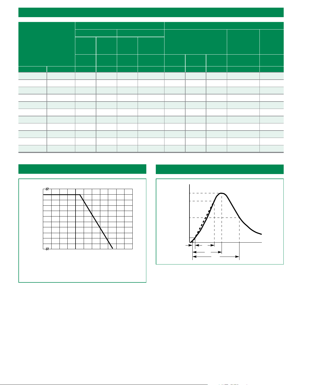
Power Dissipation Ratings
100
90
80
70
60
50
40
30
PERCENT OF RATED VALUE
20
10
0
Figure 1
NOTES:
1. Peak current Applies to applications rated up to 115VRMS. Peak
current is 30kA for applications greater than 115V.
2. Peak current applies to applications rated up to 132VRMS. Peak
Current is 30kA for applications greater than 132V.
-55 50 60 70 80 90 100 110 120 130 140 15
AMBIENT TEMPERATURE (oC)
Should transients occur in rapid succession, the
average power dissipation required is simply the energy
(watt- seconds) per pulse times the number of pulses
per second. The power so developed must be within
the specifications shown on the Device Ratings and
Specifications table for the specific device. Furthermore,
the operating values need to be derated at high
temperatures as shown above. Because varistors can only
dissipate a relatively small amount of average power they
are, therefore, not suitable for repetitive applications that
involve substantial amounts of average power dissipation.
Peak Pulse Current Test Waveform
100
90
50
PERCENT OF PEAK VALUE
10
O
1
Figure 2
01 = Virtual Origin of Wave
T = Time from 10% to 90% of Peak
T1 = Rise Time = 1.25 x T
T2 = Decay Time
Example - For an 8/20 μs Current Waveform:
8μs = T1 = Rise Time
20μs = T2 = Decay Time
T
T
1
T
2
TIME
DA/DB Varistor Series
146
Revision: January 9, 2009
©2008 Littelfuse, Inc.
Please refer to www.littelfuse.com/series/da or /db.html for current information.
Specifications are subject to change without notice.
Maximum Clamping Voltage
V131DA40 - V751DA40 and V131DB40 - V751DB40
6,000
MAXIMUM CLAMPING VOLTAGE
5,000
DISC SIZE 40mm
MAXIMUM PEAK VOLTS (V)
Figure 3
4,000
130 TO 750 VM(AC) RATING
3,000
V511DA/DB40
V481DA/DB40
2,000
V421DA/DB40
1,000
900
800
700
600
500
400
V151DA/DB40
300
V131DA/DB40
200
-210-1100
10
PEAK AMPERES (A)
10110
V751DA/DB40
V661DA/DB40
V571DA/DB40
2
TA = -55oC to 85oC
V321DA/DB40
V271DA/DB40
V251DA/DB40
10310410
Repetitive Surge Capability
V131DA40 - V751DA40 and V131DB40 - V751DB40
50,000
20,000
10,000
SURGE CURRENT (A)
5
Figure 4
1
5,000
2
10
2,000
3
10
1,000
500
200
100
50
INDEFINITE
20
10
20 100 1,000 10,000
2
10
IMPULSE DURATION (μs)
DISC SIZE 40mm
V131DA40 - V751DA40
V131DB40 - V751DB40
4
10
5
10
6
10
NOTE: If pulse ratings are exceeded, a shift of V
+/-10% could result. This type of shift, which normally results in a decrease of V
result in the device not meeting the original published specifications, but it does not
prevent the device from continuing to function, and to provide ample protection.
(at specified current) of more than
N(DC)
N(DC)
Physical Specifications
Lead Material
Insulating Material
Device Labeling
DA - Copper, Tin–plated
DB - Brass, Tin–plated
Cured, flame retardant epoxy polymer
meets UL94V–0 requirements.
Marked with LF, part number and date
code
, may
Environmental Specifications
Operating/Storage
Temperature
Humidity Aging
Thermal Shock
Solvent Resistance MIL–STD–202, Method 215F
Moisture Sensitivity Level 1, J–STD–020C
-55°C to +85°C/ -55°C to
+125°C
+85°C, 85% RH, 1000 hours
+/- 5% typical resistance
change
+85°C to -40°C 10 times
+/- 5% typical resistance
change
©2008 Littelfuse, Inc.
Specifications are subject to change without notice.
Please refer to www.littelfuse.com/series/da or /db.html for current information.
147
Revision: January 9, 2009
HI–ENERGY MOV’S DA/DB Series
DA/DB Varistor Series
 Loading...