

Page 1

TECHNICAL MANUAL
GATES ONE - 994 9202 002
GATES TWO - 994 9203 002
GATES FIVE (1-PHASE) - 994 9204 002
GATES Series™
AM TRANSMITTERS
GATES FIVE (3-PHASE) - 994 9205 002
T.M. No. 888-2314-001
© Copyright 1990, 1991, 1992, 1994, 1995, 1996, 1998, 1999,
2000, 2001, 2002
Harris Corporation
All rights reserved
Printed: 1990
Rev. AF: 06-21-02
Page 2

Returns And Exchanges
Damaged or undamaged equipment should not be returned unless written approval and a
Return Authorization is received from HARRIS CORPORATION, Broadcast Systems Division. Special shipping instructions and coding will be provided to assure proper handling.
Complete details regarding circumstances and reasons for return are to be included in the
request for return. Custom equipment or special order equipment is not returnable. In those
instances where return or exchange of equipment is at the request of the customer, or
convenience of the customer, a res tocking fee will be charged. All returns will be sent
freight prepaid and properly insured by the customer. When communicating with HARRIS
CORPORATION, Broadcast Systems Div ision, specify the HARRIS Order Number or Invoice Number.
Unpacking
Carefully unpack the equipment and preform a visual inspection to determine that no apparent damage was incurred during shipment. Retain the shipping materials until it has been
determined that all received equipment is not damaged. Locate and retain all PACKING
CHECK LISTs. Use the PACKING CHECK LIST to help locate and identify any components
or assemblies which are removed for shipping and must be reinstalled. Also remove any
shipping supports, straps, and packing materials prior to initial turn on.
Technical Assistance
HARRIS Technical and Troubleshooting assistance is available from HARRIS Field Service
during normal business hours (8:00 AM - 5:00 PM Central Time). Emergency service is
available 24 hours a day. Telephone 217/222-8200 to contact the Field Service Department
or address correspondence to Field Service Department, HARRIS CORPORATION, Broadcast Systems Division, P.O. Box 4290, Quincy, Illinois 62305-4290, USA. Technical Support
by e-mail: tsupport@harris.com. The HARRIS factory may also be contacted through a FAX
facility (217/221-7096).
Replaceable Parts Service
Replacement parts are available 24 hours a day, seven days a week from the HARRIS
Service Parts Department. Telephone 217/222-8200 to contact the service parts department
or address correspondence to Service Parts Department, HARRIS CORPORATION, Broadcast Systems Division, P.O. Box 4290, Quincy, Illinois 62305-4290, USA. The HARRIS factory may also be contacted through a FAX facility (217/221-7096).
NOTE
The # symbol used in the parts list means used with (e.g. #C001 = used with C001).
Page 3

MANUAL REVISION HISTORY
GATES Series™ AM Transmitters
888-2314-xxx
Rev.
A April 1990 None Replaced the following pages: Title Page, v, vii, 2-1 thru 2-6, 3-3, 3-4, 4-3, 4-4, 5-1 thru 5-6, J-3, & J-4
B Aug. 1990 None Replaced the following pages: Title Page, v, 3-5, 3-6, 4-1 thru 4-4, A-1, B-1, B-2, C-2, E-3, F-1 thru F-3,
C Aug. 1990 35969 Replaced the following pages: Title Page, MRH-1/MRH-2, C-4, & C-5
D Aug. 1990 Field
E Sept. 1990 36322 Replace the following pages: Title Page, MRH-1/MRH-2, & all of Section VI
F Oct. 1990 36415 Replace the following pages: Title Page, MRH-1/MRH-2, & all of Section A
G Jan. 1991 Errata
H June 1991 FS
I July 1991 36962 Replace the following pages: Title Page, MRH-1/MRH-2, and K-3
J Aug. 1991 36963 Replace the following pages: Title Page, MRH-1/MRH-2, 6-9 to 6-12, & J-9 TO J-11
K Jan. 1992 37611 &
L June 1992 37442 Replaced Title Page, MRH-1/MRH-2 and pages 6-14 to 6-17
M Jan. 1994 38809 Replaced Title Page, MRH-1/MRH-2, page K-3, and all of section VI
N Feb. 1994 38895 Replaced Title Page, MRH-1/MRH-2, and pages F-4 & F-5
P July 1994 39302 Replaced Title Page, MRH-1/MRH-2, and all of section VI
R Dec. 1994 39223 Replaced Title Page, MRH-1/MRH-2, and pages F-4 & F-5
S July 1995 39125 Replaced Title Page, MRH-1/MRH-2, and all of section VI
T Jan. 1996 41051R Replaced Title Page, MRH-1/MRH-2, Table of Contents, 1-2 to 1-4, all of sections 2, 4, & 5
U Jan. 1996 41051R Replaced Tit le Page, MRH-1/MRH-2, and pages 6-15 to 6-19
V Mar. 1996 TBD Replaced Title Page, MRH-1/MRH-2, and page 2-9
X Dec. 1996 41575 Replaced Title Page, MRH-1/MRH-2, iv thru vi, and all of Section C
Y May 1998 42198 Replaced Title Page, MRH-1/MRH-2, and page 2-4
Y1 10-02-98 42359 Replaced Title Page, MRH-1/MRH-2, page G-6 and all of Section VI
Z 12-22-98 38895A Replaced Title Page, MRH-1/MRH-2, and all of Section F
Z1 2-15-99 42544 Replaced Title Page, MRH-1/MRH-2, and pages C-4 & C-5.
Z2 2-25-99 42636 Replaced Title Page, MRH-1/MRH-2, and all of Section VI
AA 08-18-99 45024 Replaced Title Page, MRH-1/MRH-2, and all of Section H
AB 12-10-99 45544 Replaced Title Page, MRH-1/MRH-2 and pages 2-4 and 2-5
AC 02-20-00 45748 Replaced Title Page, MRH-1/MRH-2 and all of Section II
AD 10-04-01 47730 Replaced Title Page, MRH-1/MRH-2 and page 3-6
AD1 01-15-02 47924 Replaced Title Page, MRH-1/MRH-2, and all of Section VI
AE 03-05-02 48100 Replace Title Page, MRH1/MRH2, all parts lists and chapter B.
AF 06-21-02 48426 Replace Title Page, MRH1/MRH2, and page C-3
Date ECN
Service
Request
FS
Request
Request
Misc
Pages Affected
Added MRH-1/MRH-2
G-1 thru G-4, J-1, J-2, J-3, J-4, J-9 thru J-11, & K-3
Replace the following pages: Title Page, MRH-1/MRH-2, & 2-5
Replace the following pages: Title Page, MRH-1/MRH-2, & all of Section VI
Replace the following pages: Title Page, MRH-1/MRH-2, 2-6, G-2, & J-3
Replaced Title Page, MRH-1/MRH-2 and all part lists in manual
888-2314-001 MRH-1/MRH-2
Page 4

Page 5
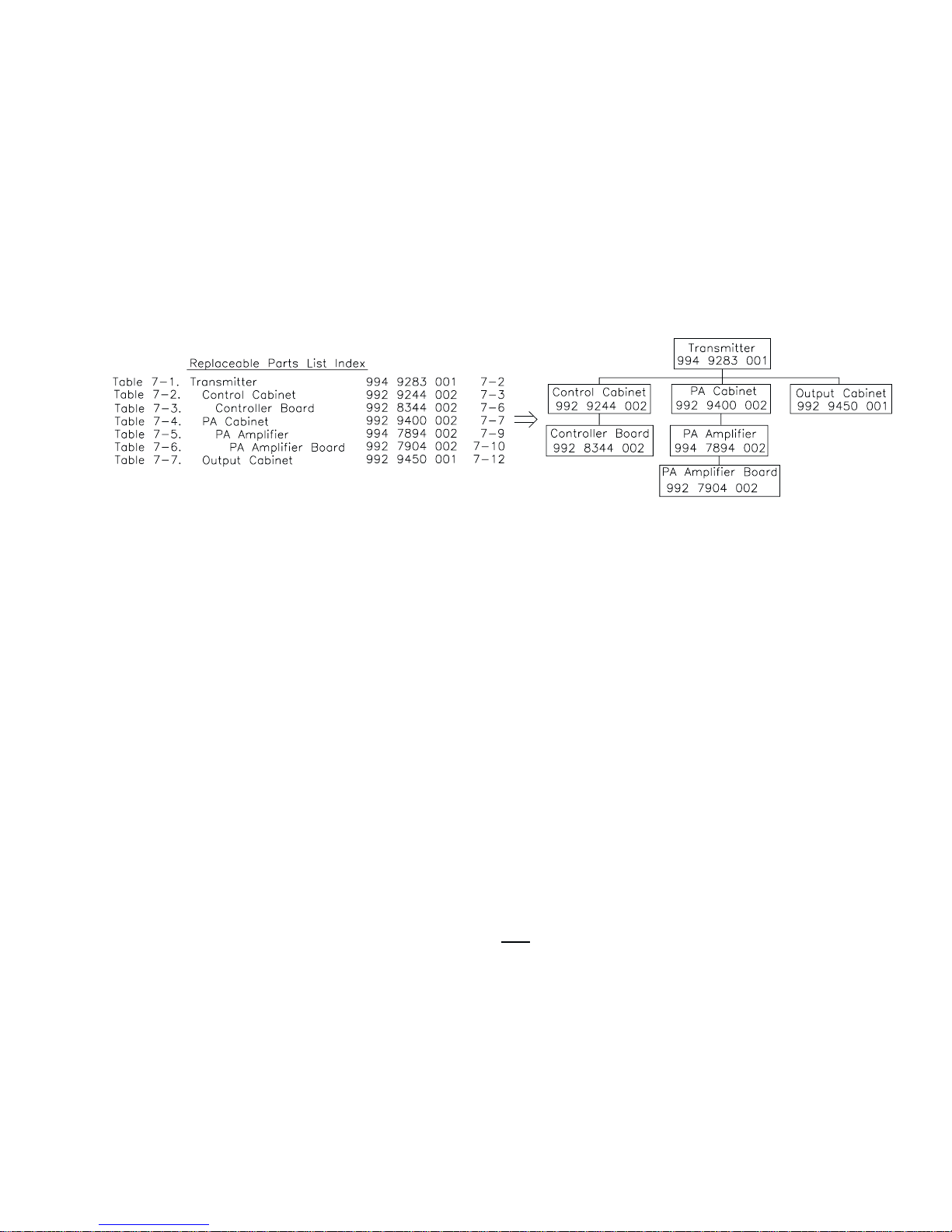
Guide to Using Harris Parts List Information
The Harris Replaceable Parts List Index portrays a tree structure with the major items being leftmost in the index. The
example below shows the Transmitter as the highest item in the tree structure. If you were to look at the bill of materials
table for the Transmitter you would find the Control Cabinet, the PA Cabinet, and the Output Cabinet. In the Replaceable
Parts List Index the Control Cabinet, PA Cabinet, and Output Cabinet show up one indentation level below the Transmitter
and implies that they are used in the Transmitter. The Controller Board is indented one level below the Control Cabinet so
it will show up in the bill of material for the Control Cabinet. The tree structure of this same index is shown to the right of
the table and shows indentation level versus tree structure level.
Example of Replaceable Parts List Index and equivalent tree structure:
The part number of the item is shown to the right of the description as is the page in the manual where the bill for that part
number starts.
Inside the actual tables, four main headings are used:
Table #-#. ITEM NAME - HARRIS PART NUMBER -this line gives the information that corresponds to the Replaceable Parts List Index entry;
HARRIS P/N column gives the ten digit Harris part number (usually in ascending order);
DESCRIPTION column gives a 25 character or less description of the part number;
REF. SYMBOLS/EXPLANATIONS column 1) gives the reference designators for the item (i.e., C001, R102, etc.) that
corresponds to the number found in the schematics (C001 in a bill of material is equivalent to C1 on the schematic) or
2) gives added information or further explanation (i.e., “Used for 208V operation only,” or “Used for HT 10LS only,”
etc.).
Inside the individual tables some standard conventions are used:
A # symbol in front of a component such as #C001 under the REF. SYMBOLS/EXPLANATIONS column means that
this item is used on or with C001 and is not the actual part number for C001.
In the ten digit part numbers, if the last three numbers are 000, the item is a part that Harris has purchased and has not
manufactured or modified. If the last three numbers are other than 000, the item is either manufactured by Harris or is
purchased from a vendor and modified for use in the Harris product.
The first three digits of the ten digit part number tell which family the part number belongs to - for example, all
electrolytic (can) capacitors will be in the same family
have a 9xx xxxx xxx part number (a number outside of the normal family of numbers), it has probably been modified
in some manner at the Harris factory and will therefore show up farther down into the individual parts list (because
each table is normally sorted in ascending order). Most Harris made or modified assemblies will have 9xx xxxx xxx
numbers associated with them.
The term “SEE HIGHER LEVEL BILL” in the description column implies that the reference designated part number
will show up in a bill that is higher in the tree structure. This is often the case for components that may be frequency
determinant or voltage determinant and are called out in a higher level bill structure that is more customer dependent
than the bill at a lower level.
(524 xxxx 000). If an electrolytic (can) capacitor is found to
Rev. X 888-2314-001 iii
WARNING: Disconnect primary power prior to servicing.
Page 6
iv 888-2314-001 Rev. X
WARNING: Disconnect primary power prior to servicing.
Page 7

WARNING
THE CURRENTS AND VOLTAGES IN THIS EQUIPMENT ARE DANGEROUS. PERSONNEL MUST
AT ALL TIMES OBSERVE SAFETY WARNINGS, INSTRUCTIONS AND REGULATIONS.
This manual is intended as a general guide for trained and qualified personnel who are aware of the dangers inherent in
handling potentially hazardous electrical/electronic circuits. It is not intended to contain a complete statement of all safety
precautions which should be observed by personnel in using this or other electronic equipment.
The installation, operation, maintenance and service of this equipment involves risks both to personnel and equipment, and
must be performed only by qualified personnel exercising due care. HARRIS CORPORATION shall not be responsible for
injury or damage resulting from improper procedures or from the use of improperly trained or inexperienced personnel
performing such tasks.
During installation and operation of this equipment, local building codes and fire protection standards must be observed.
The following National Fire Protection Association (NFPA) standards are recommended as reference:
- Automatic Fire Detectors, No. 72E
- Installation, Maintenance, and Use of Portable Fire Extinguishers, No. 10
- Halogenated Fire Extinguishing Agent Systems, No. 12A
WARNING
ALWAYS DISCONNECT POWER BEFORE OPENING COVERS, DOORS, ENCLOSURES, GATES,
PANELS OR SHIELDS. ALWAYS USE GROUNDING STICKS AND SHORT OUT HIGH VOLTAGE
POINTS BEFORE SERVICING. NEVER MAKE INTERNAL ADJUSTMENTS, PERFORM MAINTENANCE OR SERVICE WHEN ALONE OR WHEN FATIGUED.
Do not remove, short-circuit or tamper with interlock switches on access covers, doors, enclosures, gates, panels or shields.
Keep away from live circuits, know your equipment and don’t take chances.
WARNING
IN CASE OF EMERGENCY ENSURE THAT POWER HAS BEEN DISCONNECTED.
WARNING
IF OIL FILLED OR ELECTROLYTIC CAPACITORS ARE UTILIZED IN YOUR EQUIPMENT, AND IF
A LEAK OR BULGE IS APPARENT ON THE CAPACITOR CASE WHEN THE UNIT IS OPENED FOR
SERVICE OR MAINTENANCE, ALLOW THE UNIT TO COOL DOWN BEFORE ATTEMPTING TO
REMOVE THE DEFECTIVE CAPACITOR. DO NOT ATTEMPT TO SERVICE A DEFECTIVE CAPACITOR WHILE IT IS HOT DUE TO THE POSSIBILITY OF A CASE RUPTURE AND SUBSEQUENT
INJURY.
Rev. X 888-2314-001 v
WARNING: Disconnect primary power prior to servicing.
Page 8
vi 888-2314-001 Rev. X
WARNING: Disconnect primary power prior to servicing.
Page 9

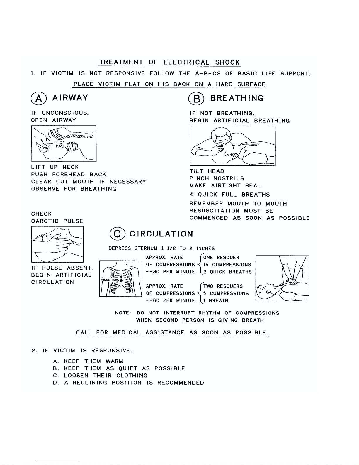
FIRST-AID
Personnel engaged in the installation, operation, maintenance or servicing of this equipment are urged to become familiar
with first-aid theory and practices. The following information is not intended to be complete first-aid procedures, it is a
brief and is only to be used as a reference. It is the duty of all personnel using the equipment to be prepared to give
adequate Emergency First Aid and thereby prevent avoidable loss of life.
Treatment of Electrical Burns
1. Extensive burned and broken skin
a. Cover area with clean sheet or cloth. (Cleanest available cloth article.)
b. Do not break blisters, remove tissue, remove adhered particles of clothing, or apply any salve or ointment.
c. Treat victim for shock as required.
d. Arrange transportation to a hospital as quickly as possible.
e. If arms or legs are affected keep them elevated.
NOTE
If medical help will not be available within an hour and the victim is
conscious and not vomiting, give him a weak solution of salt and
soda: 1 level teaspoonful of salt and 1/2 level teaspoonful of baking
soda to each quart of water (neither hot or cold). Allow victim to sip
slowly about 4 ounces (a half of glass) over a period of 15 minutes.
Discontinue fluid if vomiting occurs. (Do not give alcohol.)
REFERENCE:
2. Less severe burns - (1st & 2nd degree)
a. Apply cool (not ice cold) compresses using the cleanest available cloth article.
b. Do not break blisters, remove tissue, remove adhered particles of clothing, or apply salve or ointment.
c. Apply clean dry dressing if necessary.
d. Treat victim for shock as required.
e. Arrange transportation to a hospital as quickly as possible.
f. If arms or legs are affected keep them elevated.
ILLINOIS HEART ASSOCIATION
AMERICAN RED CROSS STANDARD FIRST AID AND PERSONAL SAFETY MANUAL (SECOND EDITION)
Rev. X 888-2314-001 vii
WARNING: Disconnect primary power prior to servicing.
Page 10

TABLE OF CONTENTS
SECTION I
GENERAL INFORMATION
Introduction......................................1-1
ScopeAndPurpose..............................1-1
Specifications....................................1-1
SECTION II
INSTALLATION/OPERATION
Introduction......................................2-1
Unpacking.......................................2-1
ReturnsandExchanges.............................2-1
GeneralInstallationInformation .....................2-1
Power Distribution for Optimum Transmitter Perform-
ance .........................................2-1
OverheatingfromLineUnbalance..............2-1
TransmitterNoisePerformance ................2-1
TheCausesofLineUnbalance.................2-1
ThreePhaseDeltaDistributionTransformers..... 2-2
ThreePhaseWyeDistributionTransformers...... 2-2
General Installation
Requirements ...................................2-2
EquipmentPlacement............................2-2
Pre-InstallationInspection ........................2-2
EquipmentPositioning...........................2-3
Ground Strap Installation ......................... 2-3
ElectricalInstallation ..............................2-3
PowerRequirements.............................2-3
Procedure. .................................2-3
RFOutputConnection........................... 2-4
BatteryInstallation.............................. 2-4
Audio Input .................................... 2-4
RemoteControl.................................2-4
AirflowSensorStatus............................ 2-5
FailsafeConnection..............................2-5
Modulation Monitor Sample ......................2-5
InitialTurnOnProcedure...........................2-5
InitialTurnOn .................................2-5
Modulation Monitor Carrier Level.................. 2-6
ApplicationofAudio ............................2-7
RemoteMeterCalibration ........................2-7
SECTION III
MAINTENANCE
Introduction......................................3-1
StationRecords...................................3-1
Maintenance Logbook ........................... 3-1
PreventiveMaintenance............................3-1
Maintenance Of Components ...................... 3-1
AirSystem.....................................3-2
GATES Series™ Top Removal
Procedure ....................................3-2
LowVoltageSupplyAdjustment...................3-2
High Voltage Supply Adjustment ..................3-4
RFDriveMeasurement........................... 3-4
IPATuning.................................... 3-5
PAVoltageElectricalZero ....................... 3-5
PAVoltMeterCalibration........................3-5
PACurrentCalibration........................... 3-5
Power Supply Current Calibration .................. 3-5
viii 888-2314-001 Rev. X
WARNING: Disconnect primary power prior to servicing.
PowerOutputCalibration........................ 3-5
OverloadAdjustmentProcedures.................. 3-6
Power Supply Current Overload ............... 3-6
UnderdriveFault............................ 3-6
VSWRDetector............................ 3-6
Replacing Boards and
ReplacingBoardComponents ..................... 3-6
SECTION IV
TROUBLESHOOTING
Introduction ..................................... 4-1
Definition of
FrontPanelIndicators ............................ 4-1
Symptom: Transmitter Will Not Turn On - None of
the Green LED’s on the Power Level Switches are Il-
luminated....................................... 4-1
PossibleCauses................................ 4-1
LossofACPower .......................... 4-1
ControlSupplyFailure....................... 4-1
Symptom: Green Power Level Status LED’s Illumi-
nate, but the Primary Contactors Do Not Energize and
NoOverloadLED’sIlluminate..................... 4-1
PossibleCauses................................ 4-1
Phase Monitor (3∅ FIVEonly)................ 4-1
Blownfuse................................ 4-1
OpenInterlock............................. 4-1
FailsafeInterlockOpen ...................... 4-1
InterfaceboardOutput....................... 4-1
OpenContactorCircuit ...................... 4-1
ContactorControlSignal..................... 4-1
Symptom: One or Both Primary Contactors Energize,
ButThereIsNoPowerOutput ..................... 4-1
HighVoltageSupplyFailure...................... 4-1
Symptom: High Voltage Is Present, But There Is No
PowerOutput ................................... 4-2
PDMKillCondition ............................ 4-2
PDMLevel.................................... 4-2
PossibleCausesForOverloads...................... 4-2
Supply Voltage Overload ........................ 4-2
Supply Voltage Too High .................... 4-2
Power Supply Current Overloads- At Turn On ....... 4-2
Supply Short ............................... 4-2
Power Supply Current Overloads, Continuous Cycling
andAutomaticCutback......................... 4-2
PDMSystemProblem....................... 4-2
PDMGeneratorOutputsHigh................. 4-2
PDMAmplifierShorts....................... 4-2
Supply Current Calibration ................... 4-2
Random Supply Current Overloads With Modulation. . 4-2
Sub-audibleSignals......................... 4-2
UnderdriveFault ............................... 4-2
Low/NoDrive.............................. 4-2
IPAandPATransistors...................... 4-2
VSWR Overload- Continuous VSWR Cycling ....... 4-2
BadLoadImpedance........................ 4-2
AntennaProblem........................... 4-3
OutputNetwork............................ 4-3
Page 11

VSWR Trips With High Levels Of Modulation and
HighPower................................... 4-3
ImproperTuningandLoading................. 4-3
Antenna .................................. 4-3
OutputNetwork............................ 4-3
Symptom:RemoteControlFunctionsDoNotWork .... 4-3
PossibleCauses................................ 4-3
Remote/LocalSwitch........................ 4-3
RemoteControlImproperlyWired............. 4-3
RemoteControlUnitNotFunctioning.......... 4-3
RibbonConnectorsLoose.................... 4-3
CausesforaPAVolts/PAAmpsRatioChange ........ 4-3
No+20VoltstoPDMAmplifier.................. 4-3
ImpedanceChange ............................. 4-3
PAFailure.................................... 4-3
Troubleshooting AM Noise......................... 4-4
50/60Hz...................................... 4-4
AudioLinesareNormallyBalanced ............... 4-4
100/120Hz.................................... 4-4
300/360Hz.................................... 4-4
60kHz....................................... 4-4
RFINoiseonAudio ............................ 4-4
SECTION V
TRANSMITTER OVERALL
Introduction..................................... 5-1
Personnel Protection .............................. 5-1
PrinciplesOfOperation............................ 5-1
FET’SintheGATESSeries™.................... 5-1
PDMTheoryInBrief ........................... 5-1
PolyphaseTheory .............................. 5-1
Audio/PDMSignalFlow......................... 5-1
PDMLoop.................................... 5-3
RFPowerFlow................................ 5-3
Failsafe....................................... 5-3
ACPowerFlow................................ 5-3
High Voltage Power Supply ...................... 5-3
Introduction ............................... 5-3
Description................................ 5-3
Low Voltage Power Supply and IPA Power Supply. . . 5-6
Introduction ............................... 5-6
Description................................ 5-6
AirflowSensor................................. 5-6
Introduction ............................... 5-6
Description................................ 5-6
Section VI
Parts List
Introduction..................................... 6-1
SECTION A
OSCILLATOR (A16)
PrinciplesOfOperation............................ A-1
Replacement/Alignment ........................... A-1
FrequencyAdjustment........................... A-1
Troubleshooting the
RFOscillator ................................... A-1
Symptom:NoOutput ........................... A-1
OpenFuse/Lossof+20V..................... A-1
RFKILL.................................. A-1
Q1,Q2,CR1................................ A-1
U1,CR4...................................A-1
U2.......................................A-1
U3.......................................A-1
SECTION B
IPA (A5)
PrinciplesofOperation.............................B-1
IPATuningNetwork............................B-1
Replacement/Alignment............................B-1
IPA Tuning and Testing
Procedure......................................B-1
IPATuning................................B-1
OhmmeterTestingtheIPA .......................B-1
HandlingMOSFET’s..............................B-1
TestingMOSFET’s ...............................B-2
SECTION C
POWER AMPLIFIER A1 through A4
PrinciplesofOperation.............................C-1
PAToroids......................................C-1
Replacing a PA Module............................C-1
TroubleshootingthePABoards......................C-1
OhmmeterTesting..............................C-1
HandlingMOSFET’s..............................C-2
TestingMOSFET’s ...............................C-2
ReplacingPATransistors.........................C-2
ScopingtheRFDrive..............................C-2
RFDrivePhasingMeasurement .....................C-2
SECTION D
OUTPUT NETWORK
PrinciplesofOperation.............................D-1
AdjustmentProcedures.............................D-1
TuningAndLoadingControls.....................D-1
OutputNetworkColdTuning .....................D-1
ThirdHarmonicTrapL7-C4 ..................D-1
Bandpass Filter L2-C2 .......................D-1
TEENetwork-LoadandTune................D-1
L2SlidingTap .............................D-1
L1Tap....................................D-2
SECTION E
OUTPUT MONITOR (A18)
PrinciplesofOperation.............................E-1
Replacement/Alignment............................E-1
Troubleshooting..................................E-1
Symptom: Detector Null Reading Is High and Cannot
BeAdjustedToZero............................E-1
BadLoadImpedance ........................E-1
SampleSignalMissing.......................E-1
SECTION F
PDM GENERATOR (A15)
PrinciplesOfOperation............................ F-1
Replacement/Alignment............................F-1
TroubleshootingPDMGenerator..................... F-1
Symptom: No Pulses At J4, Causing Zero Power Out-
putfromtheTransmitter......................... F-1
PowerSetting ..............................F-1
LossofPlusandMinus15Volts............... F-1
PDMInterrupt.............................. F-1
DC/AudioFailure........................... F-1
Rev. X 888-2314-001 ix
WARNING: Disconnect primary power prior to servicing.
Page 12

Symptom:ImbalanceInOutputPulseWidths ........F-2
AudioImbalance............................F-2
TriangleWaveImbalance.....................F-2
Symptom: Output(s) At J2 Always In A High State,
Causing One or More Pdm Amplifiers to Conduct
FullTime.....................................F-2
Symptom:OnlyOneOutputHigh..................F-3
Symptom:TwoOutputsAreHigh..................F-3
Symptom:AllFourOutputsAreHigh ..............F-3
SECTION G
PDM AMPLIFIER/PULL-UP (A6-A9)
PrinciplesofOperation............................ G-1
PDMAmplifier................................ G-1
PDMPull-UpBoard............................ G-1
Maintenance .................................... G-1
PDMAmplifiers............................... G-1
GateDriveChecks............................. G-1
In-Circuit Ohmmetering the PDM Amp Module (A6
thruA9)MOSFET’s........................... G-2
CheckingGateDrive........................ G-4
HandlingMOSFET’s............................. G-4
TestingMOSFET’s............................... G-4
SECTION H
PDM FILTER (A10 and A11)
PrinciplesofOperation............................ H-1
SECTION J
CONTROLLER BOARD (A12)
PrinciplesofOperation............................. J-1
CoarsePowerLevelControl ...................... J-1
ContactorControl............................... J-1
FinePowerControl.............................. J-1
Metering ...................................... J-1
OverloadCircuitry .............................. J-1
OtherFaultDetection............................ J-2
ControllerSupplyVoltages........................J-2
Replacement/AlignmentProcedures...................J-2
PAVoltageElectricalZero........................J-2
PAVoltMeterCalibration ........................J-2
Power Supply Current Calibration ..................J-2
PowerOutputCalibration.........................J-3
OverloadAdjustmentProcedures.....................J-3
Power Supply Current Overload ....................J-3
UnderdriveFault ................................J-3
VSWRDetector.................................J-3
Troubleshooting the Controller .......................J-3
Symptom: Will Not Respond To An On Command ....J-3
Controller Supply Failure ......................J-3
Failedflipflopcircuitry.......................J-3
Symptom: PDM Power Level Signal Cannot Be Con-
trolled ........................................J-3
Symptom:MultimeterIsPinnedFarLeftorRight .....J-3
Symptom: Some Remote Control Functions Do Not
Work.........................................J-3
SECTION K
INTERFACE BOARD (A24)
PrinciplesofOperation............................ K-1
Replacement/Alignment............................ K-1
Troubleshooting .................................. K-1
Symptom: Green Power Level Status LED’s Light On
Controller,ButTheContactorsDoNotEnergize.....K-1
OpenInterlock............................. K-1
24VACMissing............................ K-1
ONCommandMissing ...................... K-1
BadTriacorOpticalIsolator..................K-1
APPENDIX L
TEST EQUIPMENT
Introduction ..................................... L-1
x 888-2314-001 Rev. X
WARNING: Disconnect primary power prior to servicing.
Page 13

SECTION I
GENERAL INFORMATION
1.1. Introduction
1.1.1. Scope And Purpose
This technical manual contains the information necessary to install and maintainthe
GATES Series™ AM Transmitters. The
various sections of this technical manual
provide the following types of information.
Section I, General Information, provides introduction to technical manual contents.
Section II, Installation/operation, provides detailed installation and operation procedures.
Section III, Maintenance, provides
preventive and corrective maintenance as well as tuning procedures
(alignment procedures).
Section IV, Troubleshooting, provides a listing of the protection devices in the transmitter as well as
troubleshooting procedures.
Section V, Transmitter Overall, provides theory of operation of the various sections of the transmitter not
covered in later sections.
Section VI, Parts List, provides parts
list for the transmitter.
The following sections provideprinciples
of operation, maintenance information,
troubleshooting,and parts lists forboardsin
GATES Series™ transmitter:
Section A, Oscillator
Section B, IPA
Section C, Power Amplifier
Section D, Output Network
Section E, Output Monitor
Section F, PDM Generator
Section G, PDM Amplifier/Pull-Up
Section H, PDM Filter
Section J, Controller
Section K, Interface Board
Appendix L, Test Equipment, provides a list of the test equipment provided and recommended to perform
maintenance on the transmitter.
1.2. Specifications
Table 1-1, 1-2, and 1-3 list the specifica-
tions of the GATES Series™ transmitters.
NOTE
Specifications subject to change without
notice.
Rev. T: Jan. 1996 888-2314-001 1-1
WARNING: Disconnect primary power prior to servicing.
Page 14

Table 1-1. GATES ONE Specifications
POWER OUTPUT: 1000 watts (Rated). Six power levels adjustable between 100-1100 watts. Capable
of lower power PSA/PSSA operation.
RF FREQUENCY RANGE: 531 kHz through 1705 kHz. Supplied to one frequency as ordered.
CARRIER FREQUENCY STABILITY: Crystal control oscillator meets FCC specifications. +/-4 Hz in typical operating
environment.
RF OUTPUT IMPEDANCE: 50 ohms unbalanced.
RF OUTPUT TUNING: Integral network will match a VSWR of 1.5:1 to 1.0:1 at carrier.
RF OUTPUT TERMINAL: Type N female connector.
CARRIER SHIFT: Less than 1% at 100% modulation at 1000 Hz.
RF HARMONICS AND SPURIOUS EMISSIONS: Exceeds FCC and CCIR specifications.
OTHER EMISSIONS: Meets FCC NRSC 2 when presented with audio signal conforming to NRSC 1
standard.
TYPE OF MODULATOR: Patented Polyphase PDM.
AUDIO FREQUENCY RESPONSE: +/-0.5 dB, from 20 to 10,000 Hz (with Bessel filter out).
AUDIO HARMONIC DISTORTION: Less than 1.0% at 1 kW, 20 to 10,000 Hz @ 95% modulation.
AUDIO INTERMODULATION DISTORTION: Less than 1.0%, 60/7000 Hz 1:1. Less than 1.5%, 60/7000 Hz 4:1, SMPTE
standards at 1 kW operation at 95% modulation.
SQUAREWAVE OVERSHOOT: Less than 3.5% at 400 Hz.
SQUAREWAVE TILT: Less than 3% at 20 Hz, 90% modulation.
Less than 1.5% at 40 Hz, 90% modulation.
NOISE (UNWEIGHTED) Better t han 60 dB below 100% modulation, 1000 Hz at 1kW.
POSITIVE PEAK CAPABILITY: Greater than 130% positive peak program modulation capability at 1100 watts.
INCIDENTAL QUADRATURE MODULATION
30 dB typical below 95% modulation of L+R channel at 1 kHz.
(IQM):
AUDIO INPUT: Continuously adjustable from -10 to +10 dBm, transformer-less active 600 ohms
input.
ACVOLTAGE INPUT: 197-251 VAC, 50/60 Hz, single phase.
OVERALL EFFICIENCY: Better than 65% at 1000W.
POWER CONSUMPTION: At 1000 watts carrier, 1538 watts or less at 0% modulation, 2307 watts or less at
100% sine wave modulation, 1923 watts during typical programming.
MONITOR PROVISIONS: Adjustable to 5 volts nominal RMS modulated output sample at 50 ohms for six
power levels from 100 watts to 1100 watts.
REMOTE CONTROL/MONITORING: Self-contained interface for most remote control systems TTL compatible.
AMBIENT TEMPERATURERANGE: -10°Cto+50°C AMSL (derate upper limit 2°C per 1000 feet altitude).
AMBIENT HUMIDITY RANGE: To 95%, non condensing.
AIR FLOW: 500 CFM
HEAT GENERATED: 2756 BTU per hour at 1 KW 100% tone modulation.
ALTITUDE: Up to 13,000 feet (4000 meters).
SIZE: 72"H X 28"W X 30"D (1830mm X 712 mm X 762 mm).
WEIGHT: (Unpacked) 400 lbs. (181 kg) - approximate. Domestic packed, 600 lbs. (275 kg)
- approximate. Export packed, 700 lbs. (320 kg) - approximate.
CUBAGE: 68.7 cubic feet (2 cubic meters) packed.
NOTE: ALL SPECIFICATIONS TAKEN WITH TRANSMITTER CONNECTED TO TEST LOAD. SPECIFICATIONS SUBJECT
TO CHANGE WITHOUT NOTICE.
1-2 888-2314-001 Rev. T: Jan. 1996
WARNING: Disconnect primary power prior to servicing.
Page 15

Table 1-2. GATES TWO Specifications
POWER OUTPUT: 2500 watts (Rated). Six power levels adjustable between 250-2750 watts. Capable of
lower power PSA/PSSA operation.
RF FREQUENCY RANGE: 531 kHz through 1705 kHz. Supplied to one frequency as ordered.
CARRIER FREQUENCY STABILITY: Crystal control oscillator meets FCC specifications. +/-4 Hz in typical operating
environment.
RF OUTPUT IMPEDANCE: 50 ohms unbalanced.
RF OUTPUT TUNING: Integral network will match a VSWR of 1.5:1 to 1.0:1 at carrier.
RF OUTPUT TERMINAL: 7/8" EIA male/female flange connector.
CARRIER SHIFT: Less than 1% at 100% modulation at 1000 Hz.
RF HARMONICS AND SPURIOUS EMIS-
Exceeds FCC and CCIR specifications.
SIONS:
OTHER EMISSIONS: MeetsFCCNRSC2whenpresentedwithaudiosignalconformingtoNRSC1standard.
TYPE OF MODULATOR: Patented Polyphase PDM.
AUDIO FREQUENCY RESPONSE: +/-0.5 dB, from 20 to 10,000 Hz (with Bessel filter out).
AUDIO HARMONIC DISTORTION: Less than 1.0% at 2500 watts, 20 to 10,000 Hz @ 95% modulation.
AUDIO INTERMODULATION DISTORTION: Less than 1.0%, 60/7000 Hz 1:1. Less than 1.5%, 60/7000 Hz 4:1, SMPTE standards
at 2500 watts operation at 95% modulation.
SQUAREWAVE OVERSHOOT: Less than 3.5% at 400 Hz.
SQUAREWAVE TILT: Less than 3% at 20 Hz, 90% modulation.
Less than 1.5% at 40 Hz, 90% modulation.
NOISE (UNWEIGHTED): Better than 60 dB below 100% modulation, 1000 Hz at 2500 watts.
POSITIVE PEAK CAPABILITY: Greater than 130% positive peak program modulation capability at 2750 watts.
INCIDENTAL QUADRATURE MODULA-
30 dB typical below 95% modulation of L+R channel at 1 kHz.
TION (IQM):
AUDIOINPUT: Continuouslyadjustablefrom-10to+10dBm,transformer-lessactive600ohmsinput.
AC VOLTAGE INPUT: 197-251 VAC, 50/60 Hz, single phase.
OVERALL EFFICIENCY: Better than 65% at 2500W.
POWER CONSUMPTION: At 2500 watts carrier,3846 watts or less at 0%modulation, 5769 watts or less at 100%
sine wave modulation, 4807 watts during typical programming.
MONITOR PROVISIONS: Adjustable to5 volts nominal RMSmodulated output sample at50 ohms for sixpower
levels from 250 watts to 2750 watts.
REMOTE CONTROL/MONITORING: Self-contained interface for most remote control systems TTL compatible.
AMBIENT TEMPERATURERANGE: -10°Cto+50°C AMSL (derate upper limit 2°C per 1000 feet altitude).
AMBIENT HUMIDITY RANGE: To 95%, non condensing.
AIR FLOW: 500 CFM
HEAT GENERATED: 6895 BTU per hour at 2500 watts, 100% tone modulation.
ALTITUDE: Up to 13,000 feet (4000 meters).
SIZE: 72"H X 28"W X 30"D (1830 mm X 712 mm X 762 mm).
WEIGHT: (Unpacked) 450 lbs. (204 kg) - approximate. Domestic packed, 650 lbs. (298 kg) -
approximate. Export packed, 750 lbs. (343 kg) - approximate.
CUBAGE: 68.7 cubic feet (2 cubic meters) packed.
NOTE: ALL SPECIFICATIONS TAKEN WITH TRANSMITTER CONNECTED TO TEST LOAD. S PECIFICATIONS SUBJECT
TO CHANGE WITHOUT NOTICE.
Rev. T: Jan. 1996 888-2314-001 1-3
WARNING: Disconnect primary power prior to servicing.
Page 16

Table 1-3. GATES FIVE Specifications
POWER OUTPUT: 5000 watts (Rated). Six power levels adjustable between 500-5600 watts. Capable of
lower power PSA/PSSA operation.
RF FREQUENCY RANGE: 531 kHz through 1705 kHz. Supplied to one frequency as ordered.
CARRIER FREQUENCY STABILITY: Crystal control oscillator meets FCC specifications. +/-4 Hz in typical operating
environment.
RF OUTPUT IMPEDANCE: 50 ohms unbalanced.
RF OUTPUT TUNING: Integral network will match a VSWR of 1.5:1 to 1.0:1 at carrier.
RF OUTPUT TERMINAL: 7/8" EIA male/female flange connector.
CARRIER SHIFT: Less than 1% at 100% modulation at 1000 Hz.
RF HAR MONICS AND SPURIOUS EMIS-
Exceeds FCC and CCIR specifications.
SIONS:
OTHER EMISSIONS: Meets FCC NRSC 2 when presented with audio signal c onforming to NRSC 1
standard.
TYPE OF MODULATOR: Patented Polyphase PDM.
AUDIO FREQUENCY RESPONSE: +/-0.5 dB, from 20 to 10,000 Hz (with Bessel filter out).
AUDIOHARMONIC DISTORTION: Less than 0.8% at 5000 watts, typically less than 1.5% at 1 kW, 20 to 10,000 Hz @
95% modulation.
AUDIO INTERMODULATION DISTORTION: Less than 1.0%, 60/7000 Hz 1:1. Less than 1.5%, 60/7000 Hz 4:1, SMPTE standards
at 5000 watts operation at 95% modulation.
SQUAREWAVE OVERSHOOT: Less than 3.5% at 400 Hz.
SQUAREWAVE TILT: Less than 3% at 20 Hz, 90% modulation.
Less than 1.5% at 40 Hz, 90% modulation.
NOISE (UNWEIGHTED): Better than 60 dB below 100% modulation, 1000 Hz at 2500 watts to 5000 watts.
POSITIVE PEAK CAPABILITY: Greater than 130% positive peak program modulation capability at 5600 watts.
INCIDENTAL QUADRATURE MODULA-
30 dB typical below 95% modulation of L+R channel at 1 kHz.
TION (IQM):
AUDIO INPUT: Continuouslyadjustable from -10 to+10dBm,transformer-lessactive600 ohms input.
ACVOLTAGE INPUT: 197-251 VAC, 50/60 Hz, three phase or international 341 to 434 VAC. Compatible
with WYE or closed delta power sources. AC voltage variation: +5, -10% for full
performance. Single phase version accepts 197 to 251 VAC 50/60 Hz.
OVERALL EFFICIENCY: Better than 65% at 5000W.
POWER CONSUMPTION: At 5000 watts carrier, 7692 watts or less at 0% modulation, 11538 watts or less at
100% sine wave modulation, 9615 watts during typical programming.
MONITOR PROVISIONS: Adjustableto 5 volts nominal RMS modulated output sample at50ohms for six power
levels from 500 watts to 5600 watts.
REMOTE CONTROL/MONITORING: Self-contained interface for most remote control systems TTL compatible.
AMBIENT TEMPERATURERANGE: -10°Cto+50°C AMSL (derate upper limit 2°C per 1000 feet altitude).
AMBIENT HUMIDITY RANGE: To 95%, non condensing.
AIR FLOW: 500 CFM, (14.16 CMM).
HEAT GENERATED: 13790 BTU per hour at 5000 watts, 100% tone modulation.
ALTITUDE: Up to 13,000 feet (4000 meters).
SIZE: 72"H X 28"W X 30"D (1830 mm X 712 mm X 762 mm).
WEIGHT: (Unpacked) 500 lbs. (230 kg) - approximate. Domestic packed, 700 lbs. (320 kg) -
approximate. Export packed, 800 lbs. (370 kg) - approximate.
CUBAGE: 68.7 cubic feet (2 cubic meters) packed.
NOTE: ALL SPECIFICATIONS TAKEN WITH TRANSMITTER CONNECTED TO TEST LOAD. SPECIFICATIONS SUBJECT
TO CHANGE WITHOUT NOTICE.
1-4 888-2314-001 Rev. T: Jan. 1996
WARNING: Disconnect primary power prior to servicing.
Page 17

SECTION II
INSTALLATION/OPERATION
2.1. Introduction
This section of the technical manual provides detailed installation procedures and
setup instructions for the GATES Series™
AM transmitters.
Under normal conditions, the GATES Series™ T ransmitters are shipped completely
assembled and ready for installation. However ,if adverseshipping conditions are anticipated, certain components may be removed
for transport in which case these components
will be properly identified with appropriate
instructions for reinstalling the components
and making wiring connections.
2.2. Unpacking
Carefully unpack the transmitter and perform a visual inspection to determine that no
apparent damage was incurred during shipment.Retain theshippingmaterialsuntil ithas
been determined that the unit isnot damaged.
The contents of the shipment should be as
indicatedonthePackingCheckListwhich
accompanies each shipment. If the contents
are incomplete or if the unit is damaged electricallyormechanically ,notifytheCARRIER
and HARRIS CORPORATION.
2.3. Returns and Exchanges
Damaged or undamaged equipment should
not be returned unless written approval and a
ReturnAuthorizationisreceivedfrom HARRIS
CORPORATION, Broadcast TransmissionDivision.Special shipping instructions and coding
will be provided to assure proper handling.
Complete details re garding circumstances and
reasonsforreturnaretobeincludedinthe
requestforreturn.Customequipmentorspecial
order equipment is not returnable. In those instances where return or exchange of equipment
isat the request of the customer ,or conv enience
ofthe customer,arestockingfeewillbe charged.
Allreturnswill be sent freightprepaidandproperly insured by the customer .When communicating with HARRIS CORPORATION,
Broadcast Transmission Division, specify the
Factory Order Number or InvoiceNumber.
2.4. General Installation Information
The GATES Series™ Transmitters have
been designed for rapid installation. In addition to the 28 inch width by 30 inchdepth
of the equipment, a minimum of 24 inches
should be allowed for maintenance access
from both the front and rear of the cabinet.
Signal and power wires can be connected
through several different entries or any desired c ombination thereof.
The holes for cable entrance are 2 inches
in diameter, and are located at the front and
rear bottom of each side panel. These entriesprovidea means to entertheequipment
with wires that are then routed into the base
of the equipment.
Input powerwiresshouldrun to the terminal board installed in the base of the transmitter. Access to this terminal board is
gainedby removing the coverplate overthe
face of the contactor chassis. The screws
holding the chassis must then be removed
and the chassis pulled forward.
The normal air flow through the transmitter is taken in through the back of the unit
(at the bottom of the cabinet). Maximum
temperature at the base of the transmitter
should not be more than 50°C. The air
moves from the base of the cabinet into the
side panels and into themain enclosure. Air
passes over the heat sink fins in the side
panelsand exits through the holes inthetop
ofthe cabinet. This providesefficientchimney action cooling of all the Power Amplifier and Modulator transistors.
The air that enters the main enclosure
passes directly over the components dissipating heat and exhauststhroughtheoutput
coils and out the top of the transmitter. The
circuit cards and their heat sinks have been
designed to provide a chimney action to the
maximum extent practical.
NOTE
Note that the two blowers have separate
air intakes. One is filtered and the other
is not. The unfiltered side is dedicated to
the PA side wall. No filter is needed be-
cause most of the air passes through the
heat sink fins. A small amount of air is
channeled in the cabinet to flush the PA
Toroids. At approximately one year in-
tervals, the PA heat sink fins should be
inspected and cleaned. They may be re-
moved by removing the 10/32 mounting
screws.
2.4.1. Power Distribution for Optimum
Transmitter Performance
(This section is applicable to the three
phase GATES FIVE only, as well as other
three phase equipment.)
For many years HARRIS engineers have
recommended that the three phase power
distribution system should be either a
closed delta or W YE configuration to provide better radio and television transmitter
performanceby helping preventlineunbalance. Operation with substantial voltage
unbalance from line toline results in higher
than normal signal-to-noise ratio in the
transmitter output signal, increased three
phase transformer heating, and hot three
phase motors.
2.4.1.1. Overheating from Line Unbalance
Evenadeviceassimpleasathreephase
motor should be operated from a power line
in which the voltage is balanced within 1%. It
takes only a 3.5% line unbalance to produce
a 25% increase above normal temperature. A
5%unbalancewillcausedestructivetemperature rises of 50% greater than normal!
Similar characteristics can be expected in
the windings of a three phase power transformer down inside the cabinet of your transmitter. Transformers and motors can be
designedwithextrasafetyfeatureswherethermal rise is limited to acceptable levels; however ,in this case, other transmitter parameters
cannot be made acceptable at a reasonable
cost.
2.4.1.2. Transmitter Noise Performance
The most difficultparameter to meet with
power line unbalance is transmitter noise
performance. Most large transmitters use
six-phase or twelve-phase high voltage
power supplies. The energy storage capacitors are expensiveto install and largestored
energiesmake destructive faults inevitable.
A good design will have sufficient energy
storage capacitors to meet thespecifiedsignal-to-noise but not much more. When the
equipment is then operated from an unbalanced line, the power supply ripple frequency will be twice the line frequency
instead of six to twelve times. It becomes
obvious that it would take three times as
much energy storage to achieve the original
performance goal.
2.4.1.3. The Causes of Line Unbalance
How does a line unbalance occur? It is a
rare case in w hich a large commercial
powerproducer would generateunbalanced
voltage, so we must look elsewhere in the
system. When you have large single phase
power u sers on a power line this can cause
uneven distribution of the line currents in
the system. Uneven currents through balanced impedances will result in line-to-line
voltage unbalance.
Another likely source of this problem can
come from unbalanced impedances in the
power distribution system. Unbalanced impedance will always be seen when an
“open” delta three phase distribution system is used. Transformer design textbooks
Rev. AC: 2/29/00 888-2314-001 2-1
WARNING: Disconnect primary power prior to servicing.
Page 18

clearly show that the voltage regulation of
an unbalanced system is poor.
2.4.1.4. Three Phase Delta Distribution
Transformers
Figure 2-1 shows open and closed delta
systems. The closed delta impedance looking into each terminal (A, B & C) is exactly
thesame;butthisisnotthecaseintheopen
delta configuration. Depending on the impedances of the transformers in the open
delta circuit, line voltage unbalance sufficient to impair satisfactory operation of the
overall transmitter may result. For this reason, along with their inherent susceptibility
to transients, Harris does not recommend
the use of open delta systems.
over voltage spikes. These units are limited
in the amount of energy that can be dissipated, but will handle, if designed properly,
very large currents. You can’t take a direct
lightning hit and still operate, but not many
things will. It has been reported by engineers that installation of a thirdtransformer
and trans ient protection devices, have
eliminated the difficulty.
2.4.1.5. Three Phase Wye Distribution
Transformers
The WYE connected system is also considered a symmetrical form of three phase
power distribution. All impedances are balanced as seen from each terminal (see Figure 2-2). It is important when using a WYE
connected system that the fourth wire (neutral) is connected to the mid-point of the
system as shown in the diagram. When this
connectionismadeit providesa path for the
zerosequencecurrentsaswellasanyharmonic currents which are generated due to
the rectificationof the secondary voltages.
In summary, both symmetrical power distribution systems are satisfactory because
of their balanced impedances. Use either a
closed delta or a four wire WYE system for
maximum transmitter performance. Never
use an open delta system just to cut costs it could cost dearly in the long run.
2.5. General Installation
Requirements
The key to a rapid and successful setup is
careful planning prior to delivery of the
system. HARRIS offers, as an option, engineering services to reviewand comment on
proposedinstallations. InadditionHARRIS
offers,as anoption,design,fabrication,and
installation services to any required level
for total integration of the system into a
facility.
Lifting Equipment
(Fork Lift, etc)
Hand Tools For opening wooden
Shims (2" by 2") Aluminum,assorted
Hand Operated
Hole Punch
900 lbs (408 kg)
capacity
crates
thicknesses
For adding 0.25"
hardware holes to
0.020" thick copper
ground strap at
transmitter ground
connection.
Figure 2-1. Three Phase Delta
Distribution Transformers
The only advantage of the open delta is
lower initial cost, and this is partiallyoffset
by the fact that when only two transformers
are used, they must be larger than the three
transformers in a closed delta system.
Difficulties have often been experienced
with open delta systems; but when a third
transformerwasaddedtoclose thedelta,the
problems disappeared.
Thereisanother problem which can occur
with an open delta system, and that i s
caused by lightning and switching transients. When lightning strikes or heavy
loads are switched on a power distribution
system, high voltage transients are propagated throughout the system. Unbalanced
impedances will enhance these transients
and can cause transmitter damage, particularly to solid state rectifiers.
Many transmitters are located at the end
of a long transmission line which is highly
susceptible to transient phenomena. Devices such as Metal Oxide Varistors are
inexpensive and very effective in reducing
Figure 2-2. Three Phase WYE
Distribution Transformers
Today, many transformers are supplied
with all of the primary terminals available
sothateitheradeltaor WYEconnectioncan
be made. Table2-1 shows the different lineto-line voltages that are available with this
configuration.
Delta connected
transformer
WYE connected
transformer
210 364
220* 380*
230 400
240* 415*
250 433
* Typical voltages in some areas of the
world.
Table 2-1. Typical Line Voltages
Delta or WYE
Table 2-2. Special Installation
Tools and Equipment
Tra ns forme r, Low
472 1678 000 (1)
Level,A20T01
Transformer,
Power,A19T01
Table 2-3. Equipment Supplied with
Transmitter and Listed on Packing
Check List Supplied with Transmitter
2.5.1. Equipment Placement
See packing list for
part number
The transmitter should be located to permit adequate maintenance access and sufficient ventilation. Primary AC power cables
can enter the transmitter at a variety of
locations and the specific location of entry
will need to be determined on site. The
grounding strap between the transmitter
and the station earth ground must be properly connected before AC power wiring is
attached to transmitter.
2.5.2. Pre-Installation Inspection
Prior to performing the installation of the
GATES Series™ transmitter, it should be
thoroughly inspected for any connections
which may have loosenedduring shipment.
2-2 888-2314-001 Rev. AC: 2/29/00
WARNING: Disconnect primary power prior to servicing.
Page 19

This is important due to numerous high
current connections in the transmitter.
Also check that all ribbon cablesare properly locked into their respective printed circuit board connectors.
The mechanical interconnecting integrity
of the above mentioneditems is essential to
the attaining of proper transmitter operation. Although appropriate packaging and
shipping precautions are taken prior to the
equipment leaving the factory, hardware
may, in isolated cases, work loose in transit
and result in a failure.
Check for debris or loose hardware, especiallyaroundthe high current power supply
connections.
2.5.3. Equipment Positioning
Following removal of the shipping material, move the cabinet on its skid as near as
possible to its permanent position. If shipping bolts have been used, they will be
locatedateachcorneroftheskid.Remove
the bolts from the underside of the skid.
NOTE
Positioning of the cabinet is to be per-
formed by experienced personnel to pre-
vent damage to the equipment or injury
to personnel.
With a suitable lifting device, raise one
end of the transmitter cabinet sufficientlyto
permit the placing of three lengthsof circular bar stock under the cabinet. In this manner the cabinet can be efficiently and
carefully rolled off the skid.
2.5.4. Ground Strap Installation
The importance of a good groundingsystem and lightning protection can hardly be
overemphasized for reasons of personnel
safety, p rotection of the equipment, and
equipment performance. The following is
only a brief overview.
Lightning and transient energy via the
powerline or towerconnectionscanimpose
serious threats to your personal safety as
well as damage the equipment. For these
reasons you should have a good protective
earthing system to divert these forms of
energyto earth ground.Propergrounding of
theequipmentalso guards against electrical
shock hazards that would exist if the equipment failed in a way which put a hazardous
voltage on the chassis.
A good grounding system should include
substantial grounding at the tower base usingcopper ground rods and/or a buriedcopper ground screen, with copper strap used
to connect the tower base to earth ground.
A low impedance will help carry lightning
current directly into the ground instead of
into your building. Additionally, coax
shield(s)should be electricallyconnectedto
and exit the tower as near to the bottom as
practical to minimize the lightning voltage
potential carried by the coax into your
building.
For coaxes, a singlepoint of entry into the
building is best, with all connected to a
common grounding plate (or bulkhead
panel) having a low impedance connection
tothebuildingperimeter ground.Widecopper straps should be used for making the
connection from the common grounding
plate to earth ground.
Acommongroundingplate is alsothebest
locationfor coaxialsurgeprotectorsforsensitive equipment such as an STL receiver.
Ideally, this plate should also be the entry
point for all signal lines, and serve as a
single point ground for AC power surge
protection.
A good ground system should include perimeter grounding of the transmitter building using copper ground rods and copper
strap. There should also be a copper strap
running from tower ground to the building
perimeter ground.
Good grounding and shielding will help
keep stray RF current to a minimum. RF
interference usually shows up in one of
several ways, intermittent problems with
digital or remote control circuits, audio
feedback or high pitched noise. Even a
smallamountofnon-shieldedwiremakesa
very efficient antenna for RF and transient
energy. If RF is allowed into the audio
equipment,itcanberectifiedand may show
up as noise or feedback. Wire and cable
shields should normally be connected at
both ends to the equipment chassis.
Agroundstrapattachment point islocated
on the bottom, right rear, of the cabinet
behind the dust cover (uses a 10-32 brass
screw with brass washer). Use this connectionwhenutilizingasinglepointgrounding
system, attaching your ground strap to the
common grounding plate. See 839-7920044 Gates series Outline drawing.
A groundingstud is also providednearthe
AC input connections in the lower portion
of the transmitter. Use this connection for
the power line ground. It is located under
the low voltage power supply board.
2.6. Electrical Installation
NOTE
All GATES Series™ transmitters are
shipped with A19T1 and A20T1 con-
nected for 251 VAC operation. It is ad-
vised that the end user determine the ap-
propriate tap settings during the initial
turn-on. In this procedure, the trans-
former tapping is determined by the re-
sulting DC supply voltage. This ensures
that the DC supplies are operated in the
desired range.
2.6.1. Power Requirements
The GATES Series™ GATES FIVE (3
phase version) is designed to operate from
a3phase,208/240 VAC,50to60 Hz source.
Sixty ampere service is required. Use 6
gauge wire for this connection.
The single phase GATESFIVE requires a
100 amp 208/240 VAC, 50 to 60 Hz source.
Use 4 gauge wire for this connection.
The GATES TWO requires a 60 amp
208/240 VAC, 50 to 60 Hz source. Use 6
gauge wire for this connection.
The GATES ONE requires a 30 amp
208/240 VAC, 50 to 60 Hz source. Use 8
gauge wire for this connection.
There is no requirement for 120 VAC in
any case.
As an option, the low voltage circuits can
be powered from a separate circuit breaker.
Although not a requirement, thissetup sometimes is advantageous for maintenance and
troubleshooting. If you choose to wire your
transmitter this way,you will need to provide
a separate 10 amp circuit breaker.
NOTE
If service voltage is less than 208 VAC,
a higher current service may be needed.
Refer to the Outline drawing for mechanical dimensions and wire feed locations.
WARNING
ENSURE THAT ALL AC POWER IS OFF
PRIOR TO STARTING THE FOLLOWING
INSTALLATION
2.6.1.1. Procedure.
For a three phase GATES FIVE, connect 3
phaseACinput powerfromafuseddisconnect
box or circuit breaker to transmitter cabinet
terminal board TB1 terminals 1, 2 and 3. The
powersourcecan be either a closeddelta(usually 230 to 240 volts) or aWYE (usually 208).
For a four wire WYE system (341 to 434
volts), connect the neutral wire to terminal
board TB1 terminal 4. Also for a WYE
system ensure that the high voltage transformer has been tapped correctly for the
configuration (see the Wiring Diagram for
the three phase GATESFIVE transmitter).
For the GATES ONE, GATES TWO, or
single phase GATESFIVE, connect ACinput
power(197 to 251 VAC)from afused disconnect box orcircuit breaker to transmitter cabinet terminal board TB1 terminals 1 and 2.
NOTE
Terminal board TB1 is accessed by remov-
ing the four screws which hold the circuit
breaker panel to the front of the transmit-
Rev. AC: 2/29/00 888-2314-001 2-3
WARNING: Disconnect primary power prior to servicing.
Page 20
ter and then sliding the circuit breaker
panel forward. Terminal board TB1 is
located on the floor of the transmitter directly below the AC Power panel. Terminals are numbered left to right.
Ifyou choose towireyourtransmitterwith
separatelow voltageandhigh voltagefeeds,
you will need to remove the factory installedjumperwiresfrom TB1, and connect
a10ampservicetoTB1terminals5and6.
For the 3 phase GATESFIVE, ensure that
the Phase Monitor relay A19K3 is installed
Table 2-4. Interface Board Connections
CONTROL
INPUTS TERMINAL
Low TB2-1
Two TB2-2
Three TB2-3
Four TB2-4
Five TB2-5
High TB2-6
Off TB2-7
Raise TB2-8
Lower TB2-9
Ext Kill (RF mute) TB2-10
FAILSAFE TB1-1 and TB1-2
METERING
OUTPUTS TERMINAL
PA Voltage TB2-11
PS Current TB2-12
Power Output TB2-13
STATUS TERMINAL
Low TB2-15
Two TB2-16
Three TB2-17
Four TB2-18
Five TB2-19
High TB2-20
OVERLOAD
STATUS TERMINAL
Overload Ind Reset TB2-14
Auto Cutback TB2-21
Supply Voltage TB2-22
Supply Current TB2-23
Underdrive TB2-24
VSWR TB2-25
Audio TB2-26
Audio TB2-27
Ground TB2-28
in the AC Power panel and is adjusted to
MIN.SeeNotebelow.
NOTE
To adjust the Phase Monitor, remove all
power from transmitter and rotate the voltage
adjustment screw to your approximate AC
line voltage. The actual setting will have to be
determined by trial and error. Refer to paragraph 2.7.1.g for adjustment information.
2.6.2. RF Output Connection
Connect the output transmission line from
theantennato theRFOUTPUTconnectorjack
J1 located on top of the transmitter cabinet.
A GATES ONE requires a male type N
connector. Specific type N connectors are
availablefor various types of coax.
TheGATESTWOandGATESFIVErequire
a 7/8 EIA flange. Specific connectors of this
type are available for various kinds of coax.
2.6.3. Battery Installation
The purpose of the battery on the Controller
board (on the swing out panel) is to maintain
transmitter operational status during a power
interruption. It is not important to install it until
you are nearly ready to put the transmitter
into regular operation. The transmitter will
operate properly without the battery, however , po wer interruptions lasting more than
a few seconds will result in an OFF condition, and all overload lights lit.
A standard 9 volt battery will last about 2
weeks of continuous running with no AC
powerapplied.Alkalinebatterieswillgivethe
longest shelf life. It is a good idea to change
the battery after a long outage or yearly.
2.6.4. Audio Input
Route the audio cable up from the base of
the transmitter to the Interface board. The
Interface board is located in the lower left
portion of the transmitter in the front. Connecttheaudioinputwiresto terminals TB226 and TB2-27 on the Interface Board.
TB2-28is ground for the audiocable.Refer
to Table 2-4 and Figure 2-3.
2.6.5. Remote Control
Allremote controlconnectionsaremadeatthe
Interfaceboard. Cabling forremotecontrolmay
be routed up from the base of the transmitter.
To prepare wire, strip insulation back approximately 1/4" and twist strands back into
their natural position.
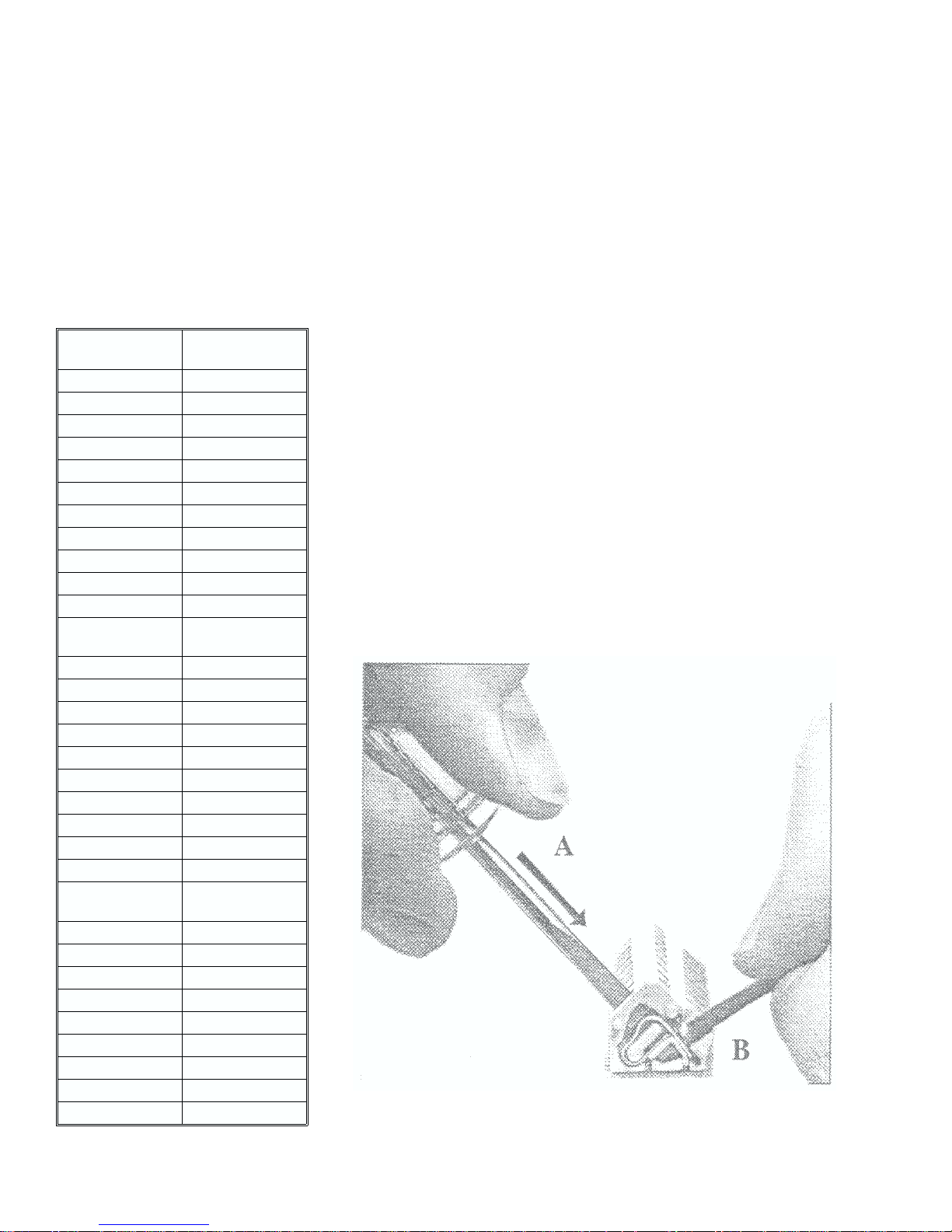
A small flat blade screwdriveris an appropriate tool to use to make the connection.
To make connection, align wire in side opening “B” and depress clamp down from
opening “A”with tool. Insert wire or component in opening “B” andsecurebywithdrawing tool.
Figure 2-3. Making Connections to WAGO Block
2-4 888-2314-001 Rev. AC: 2/29/00
WARNING: Disconnect primary power prior to servicing.
Page 21

Note:Allremotecontrol inputs areactivated
by applying a momentary ground connection
to each desired input. This makes the transmitterdirectlycompatiblewithopencollector
type remote control units as well as dry contact systems. With a dry contact (relay) system, you will simply need to momentarily
switch each of the desired control inputs to
ground in order to cause a function to occur.
The status outputs for power levels and
overloads are open collector outputs. These
are directly compatible with TTL type inputs,or may be usedto drivesmallrelays or
other indicating devices as long as the current requirements are 100 ma or less.
To use a status output to drive a small
relay, you will need to connect the relay
from the status output toa DC power source
with a positive voltage between 5 volts and
24volts.As with anyDCpoweredrelay,you
should connect a diode across the coil, with
the cathode toward the positive supply.
2.6.6. Airflow Sensor Status
In addition to the status outputs described
above, transmitters manufactured December 1995 and later are equipped with an
Airflow Sensor circuit which includes a
status output. A relay contact closure is
providedonTB1onthemainAirflowSensor circuit board, located in the air inlet for
A20B1.
All metering samples are positive with
respect to ground and are less than 5 volts
into a 10k ohm input resistance.
2.6.7. Failsafe Connection
24VAC contactor coil current passes
through the Failsafe Interlock t ermi nals.
Therefore, high voltage power supply activationrequires the presence of a continuous
closure across the Failsafe Interlock terminals. Opening of the contacts results in deenergizing the HV contactors.
A connection is required at the Failsafe
terminals even if the transmitter will be
locally controlled. Switching the transmitter to Local control does not bypass the
Failsafe interlock.
Contacts and wiring connected to these
terminalsshouldberatedfor atleast24 VAC
@ 1 amp. Refer to the listing of Interface
Board connections in the Table 2-4.
The shield connection forthe remote controlcablingshouldbe connected to a nearby
ground stud or one of the Interface board
mounting screws.
2.6.8. Modulation Monitor Sample
An adjustable, 1 to 5 Volt RMS signal
source is provided on the Output Monitor
board.The Output Monitor board is located
behind an access door on the front. Route
the cable for the modulation monitor from
the base of the transmitter up to thelocation
of the Output Monitor board. The coax will
slip into the gap between the transmitter
wallandtheenclosurefortheOutputMonitor, RF Oscillator, and PDM Generator.
Connect modulation monitor to the BNC
jackon theOutputMonitorboardA18.Besure
topositionthecoaxsafelyawayfromany
components which may generate enough heat
to melt the insulation on the coaxial cable.
2.7. Initial Turn On Procedure
Before initial t urn on, ensure that the following items are checked:
a. Ground strap is properly connected be-
tween tran smitter and station earth
ground.
b. Check for debris/hardware in base of
transmitter and in AC Panel.
c. Make sure all hardware connections are
tight.
d. AC input wiring is properly connected.
e. Transmitter output is properly termi-
nated into a suitable load capable of
handling rated output power (antenna or
dummy load).
f. Audio input is properly connected.
g. Monitoring equipment is properly con-
nected.
h. The REMOTE/LOCAL switch on the
Controller board (on the swing out
panel) should be in the local mode.
i. Be sure the front and rear covers are in
place.
2.7.1. Initial Turn On
Important
Temporarily remove F1 from the Interface
board. This will disable the contactor circuit
for the first part of the turn-on procedure.
Fasten the bottom frontpanel in place with at
least two screws.
WARNING
THE NORMAL PROCEDURE FOR
TRANSMITTER TURN OFF SHOULD BE
FOLLOWEDINORDERTOPROPERLY
DISCHARGE THE HIGH VOLTAGE COMPONENTS. TURN OFF THE HIGH VOLTAGEBYDEPRESSING THEOFF BUTTON.
IFYOUMUSTENTERTHETRANSMITTER,
SET THE REMOTE/LOCAL SWITCH TO
LOCAL AND ALLOW THE POWER SUPPLY TO DISCHARGE AS INDICATED BY
THEFRONTPANEL METERS. LOWVOLTAGE MAY THEN BE REMOVED BY SETTING THE LOW VOLTAGE CIRCUIT
BREAKER TO OFF. DISCONNECT ALL
PRIMARY POWER SERVICE. REMOVE
THE REAR LIFT OFF PANEL SLOWLY TO
ALLOW THE RESISTOR DISCHARGE
MECHANISMTOFUNCTION.AGROUNDING STICK IS PROVIDEDIN THE TRANS-
MITTER AND SHOULD BE USED TO ASSURE THAT ALL HIGH VOLTAGE HAS
BEEN REMOVED UNDER FAULT CONDITIONS. BE CAREFUL NOT TO GROUND
ANY CONNECTIONS WHICH ARE STILL
ENERGIZED.THISWOULDINCLUDE ALL
LOW VOLTAGE CIRCUITS IF THE LOW
VOLTAGE CIRCUIT BREAKER HAS NOT
BEEN SET TO OFF POSITION.
CAUTION
IF ANY ABNORMALITIES ARE ENCOUNTERED IN THE FOLLOWING STEPS, STOP
THE PROCEDURE, REMOVE ALL POWER,
AND PROCEED TO TROUBLESHOOTING
SECTION OF MANUAL.
a. Using a small blade screwdriver or ad-
justing tool, rotate the LOWpowerlevel
control pot (located below the LOW
powerON switch)severalturns counterclockwise. The other pots may be left at
the factory settings for now.
b. Apply AC power to transmitter.
c. Set the LOW VOLTAGE circuit breaker
A20CB1 to ON position.
d. Verify the +/- 12 volt supply LED’sillu-
minate on the control panel.
e. If you havea3 phase GA TESFIVE,verify
red LED on Phase Monitor (inthe contac-
tordrawer) isilluminated.Ifthe LEDisnot
illuminated, either the Phase Monitor is
not adjusted for the correct line voltage or
thephasesequenceis backwards.Remove
all po wer and adjust the volta ge selector
on the Phase Monitor to the lowest setting
and re-apply power.
f. If the LED is still not illuminated, re-
move all power and reverse any two
leads in the main disconnect box and
re-apply power and verify that the LED
is illuminated. Adjust the voltage selec-
tor so that the red LED on the Phase
Monitor relay illu minates when AC
power is applied. In this adjustment, al-
low for a reasonable sag in line voltage,
butdo not desensitize it so far that itwill
be ineffective.
Note: The Phase Monitor relay adjustment is affected only by the particular line
voltage.Itisnot affectedbythe changing of
transformer taps which may be done later.
g. Install screws holding AC Power panel
in place.
WARNING
ENSURE ALL VOLTAGE IS REMOVED
FROM TRANSMITTER AND ALL POINTS
WHERE VOLTAGE HAS BEEN APPLIED
ARE GROUNDED BEFORE CHANGING
ANY TAPSIN THE FOLLOWING STEP.
h. Use a suitable voltmeter to measure the
+/-20voltsupply. A convenientpointfor
checking these voltages is on the PDM
Rev. AC: 2/29/00 888-2314-001 2-5
WARNING: Disconnect primary power prior to servicing.
Page 22

Generator, A15 at the fuses. Measure
each voltage with respect to ground. If
the voltages are under 19 Vdc, disconnect AC power and re-tap A20T1 to the
nextlowerprimary voltage(taps240,0).
It is desired thatthe low voltage supply be
between 19 and 23 Vdc both plus and minus. Use a procedure of removing AC
power, grounding transformer taps, moving
the primary wiring to the next lower increment, then measuring +/-20 volt supplies,
to achieve the desired supply voltages.
Note: The transformer tap connections
are provided on TB3, terminals 15 through
19. Refer to Figure 2-3 for instructions on
using the Wago block terminals. Move the
AC connection as deemed appropriate to
achieve the desired output voltage.
i. Verify that all overloadand fault indica-
tors can be extinguished by pressing the
Reset button.
j. Check theRFDrivereadingontheMul-
timeter. It should be close to the values
recorded on the factory test data sheet. If
it is not, re-check the low voltage transformer tapping. If needed, check the actual RF Drive on the PA module(s) per
the procedure in Section C.
k. Confirm that when any of the power ON
pushbuttonsaredepressed theyilluminate.
The AC contactors in the pull out drawer
should not be heard energizing at this time
sinceF1isnotinthe Interfaceboard.Also,
thePDMKILLandPDMFAULTLED’s
will light in this condition.
l. Verifythat depressing the OFFpushbut-
ton clears all power ON pushbuttons.
m.Disconnect all primary power, and in-
stall F1 in place on the Interface board.
n. Reapply primary power.
o. Rotate the multimeter switchto theSup-
ply Voltage position. Depress the LOW
power pushbutton. The contactors
should close and apply main ACvoltage
tothehigh voltagesupply.Themultime-
ter should show a voltagein the rangeof
220 to 270 on the 300 scale.
WARNING
IF CONTACTORS DO NOT CLOSE IN THE
PRECEDING STEP, REMOVE ALL
POWER FROM TRANSMITTER AND ENSURE FAILSAFE INTERLOCK CONTACTS ARE JUMPERED OR EXTERNAL
FAILSAFE HIGH VOLTAGE INTERLOCK
CIRCUIT IS PROPERLY CONNECTED.
ALSO BE SURE THE REAR PANEL IS
SECURELY FASTENED.
p. Switch the multimeter to read Detector
Nullandverifythatthereadingiszero.
q. Rotate the LowPowercontrol potclock-
wise and observe the PA Voltage, PA
Amps, and FWD Power meters, and
raise the power until the power level is
as stated on the factory Final Test Data
Sheets for the Low Power setting.
r. If the Detector Null reading increases
from zero, adjust the TUNING and
LOADING controls to minimize the
reading. This will match the PA to the
load impedance you are using.
Duringtheinitial tune-up, the null should be
found to be well withinthe range of the TUNING and LOADING controls. If these controlsrequire considerable adjustment,theload
impedance on the transmitter is probably not
very close to 50 ohms. Ifconsiderable adjustment is required, the impedance presented to
the transmitter output terminal should be
measured and corrected as necessary.
Although the transmitter is designed to
match up to a 1.5:1 VSWR, the optimum
condition is to terminate it into 50 ohms.
s. Depress Power Level number 2. The
power level should increase to near the
factory setting for this power level. It
probably will not be exactly the same
since the Fine Power adjustment has not
been made.
t. AdjusttheTuningand Loading controls
as necessary to null the Detector Null
readingtozero.
u. Compare the present readings against
thefactorydataforanymajordiscrepancies. If any exist, it should be investigated at this time.
v. Progressively step the power level up-
ward by selecting each higher level,
check the readings against the Final Test
Data Sheets. Adjust the TUNING and
LOADINGcontrols to minimize the Detector Null reading to zero.
w.Compare all readings against the Test
Data. Since the High Voltage transformer is tapped at 240 +11 from the
factory, it will probably be necessary to
changethetransformertapsaccordingly.
The need to do this or not is determined
by the Supply Voltage reading on the
Multimeter.Itshouldbe250to265 volts
at full power.
A change from one transformer tap setting
to the next will produce about a 5% change in
DC Supply voltage. For example, moving
from 240, +11 to a setting of 240, 0 would
result in a DC Supply increase of about 5%.
NOTE
The smaller gauge wiring on the trans-
former primary is for the fans. These
smaller wires should always be left on
240, -11.
If you will be operating the transmitter
well below its rated power, then you may
leave the High Voltage transformer at it
highest primary setting. This will yield the
best overall performance if it is to be operating at a reduced power level.
WARNING
ENSURE ALL VOLTAGE IS REMOVED
FROM TRANSMITTER AND ALL POINTS
WHERE VOLTAGE HAS BEEN APPLIED
ARE GROUNDED BEFORE CHANGING
ANYTAPS ONTHETRANSFORMER.
x. Look at the range of the Fine Power
adjustment using the Raise/Lower
switches. It is desirable to seteach of the
coarse power level pots (LOW through
HIGH) with the Fine adjustment in the
middle portion of its range.
The PDM Power Level reading on the
Multimeter is essentially the power control
settings. This reading may serveas a handy
reference for each desired power level.
These readings should be recorded when
the transmitter is initially set up, and used
later if you need to troubleshoot a power
level change.
y. Check or set each powerlevelaccording
to your needs and compare all readings
with the factory test data. Report any
major discrepancies to the HARRIS
Service Department.
The GATES Series™ incorporates a protectiveactionnamed Automatic Cutback in
which the transmitter will step to each successivelylowerpowerinanefforttostayat
thehighesttolerable powerlevelwhen there
is an overload condition. This is similar to
the automatic foldback feature in some
transmitters, but is different in that the
power level steps down rather than going
through a gradual reduction.
Because of the Automatic Cutback feature,it isusefulto setall6 powerlevels.This
way, the transmitter output will remain at a
reasonable level should an Automatic Cutback occur. These power levels that you
would not ordinarilyuse may be intermediate power levels, or lowerthan your normal
operating powers.
2.7.2. Modulation Monitor Carrier Level
After each power level has been adjusted,
you should set the RF sample level for your
Modulation Monitor. If you are not using a
modulation monitor at the transmitter, you
should leave all of the monitor level controls
setfullycounterclockwise(minimumoutput).
The output levels of the monitor circuit are
independent of one another, so they may be set
in any order. While operating at a particular
powerlevel,rotateeach corresponding control
clockwise to achieve adequate carrier level.
Switching the REMOTE/LOCAL switch
(nearthe battery on the Controllerboard)to
2-6 888-2314-001 Rev. AC: 2/29/00
WARNING: Disconnect primary power prior to servicing.
Page 23

the REMOTE position will enable the remote control circuits and should be in REMOTE position for normal operation. In
addition to enabling the remote inputs, the
transmitter will mute the RF Oscillator
when in an OFF condition.
Note: The PA Voltmeter deflects upward
when shut off in the Remote mode. This is
a normal function of the RF drive being
removed when PA voltage is present.
2.7.3. Application of Audio
Apply audio to the transmitter, and observe the resulting modulation level on the
monitor. The audio input sensitivity is factory set for +10dBm, but is continuously
adjustabledown to -10dbm. Ifyou desire to
increasethesensitivity, you may adjust R21
on the PDM Generator.
Audio polarity is important, especially if
youoperateinstereo. Observetheresultson
yourmonitor,and change the audio polarity
if the need is indicated.
2.7.4. Remote Meter Calibration
The remote sample outputs of the transmitter are designed to be compatible with
mostmodernday remote controlunits,with
lessthan5voltsdc of output intoa10Kohm
impedance. There are no internal adjustments for these voltages.
Set the remote control unit’s calibration
adjustments to match the transmitter’sme-
ter readings.
Note: The remote current reading is Supply
Current, which is not the same as PACurrent.
The remote Supply current reading should be
calibrated against the Supply Current reading
on the transmitter multimeter.
Supply Current actually reads lower than
PA Current in normal operation due to the
manner in which the PDM system operates.
Thisconcludes the initial turn onprocedure.
Referto sections A through K for individual board controls and indicators.
Rev. AC: 2/29/00 888-2314-001 2-7
WARNING: Disconnect primary power prior to servicing.
Page 24
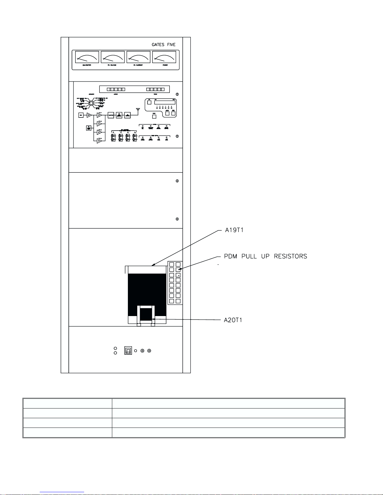
CONTROL/INDICATOR FUNCTION
Power TransformerA19T1 Main Power Supply transformer for 260 volt dc supply.
PDM Pullup Resistors Shield shown covering 250 watt resistor(s) used by PDM Pull-up circuits.
Low Voltage Transformer A20T1 Secondary for +20VDC, -20VDC, 24 VAC, and IPA Supply (60/75/90/105/120 Vdc).
2-8 888-2314-001 Rev. AC: 2/29/00
WARNING: Disconnect primary power prior to servicing.
Figure 2-4. Base of GATES Transmitter
Table 2-5. Base of GATES Transmitter
Page 25
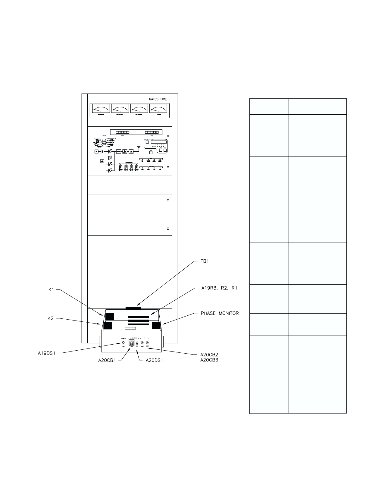
CONTROL/
INDICATOR FUNCTION
Relay K1 Relay K1 is used to
applyACtothehigh
voltage transformer
through current limiting
resistor(s) during the
step start sequence.
Relay K2 Relay K2 is used to
apply ACmains directly
to the high voltage
transformer.
Terminal Board
TB1
Step Start Resistors A19R3,
A19R2, &
A19R1
Provides connections
for AC input power.
(Only one resistor is
used in the single phase
transmitter.) The step
start resistors limit the
power supply surge
currenton initial turn on.
Phase Monitor Detects loss of phase on
primary AC input power
and h as capability to
detect low primary AC
input voltage (3 phase
GATES FIVE only).
FAN C ircuit
Breakers
A20CB2 &
Protect wiring to fans
from over current
condition.
A20CB3
Lamp A20DS1 DS1 will illuminate
whenpoweris applied to
thelowvoltagecircuitry.
Circuit Breaker,
CB1
10 Amp circuit breaker
to protect the low
volta g e power supply
from an over current
condition.
Lamp A19DS1 A19DS1 will illuminate
when power is applied
from the Main
Disconnect Switch (i.e.
cabinet is receiving AC
power).
Figure 2-5. AC Power Panel
Rev. AC: 2/29/00 888-2314-001 2-9
WARNING: Disconnect primary power prior to servicing.
Table 2-6. AC Power Panel
Controls and Indicators
Page 26

Table 2-7. GATES ONE
Typical Readings at 1340kHz
Power Output 1000W 800W 600W 400W 200W 100W
PA Volts 92.5 84 74 62 46.5 35
PA Amps 12.5 11.3 10 8.4 6.4 4.9
PDM Level 6.4 5.8 5.1 4.3 3.2 2.4
Supply Voltage 242 244 246 248 252 254
Supply Current 4.8 4.1 3.3 2.5 1.6 1.1
RF Drive 7.4 7.4 7.4 7.4 7.4 7.4
VSWR Detector Null 0 0 0 0 0 0
VSWR Detector Null Set 5.3 5.3 5.3 5.3 5.3 5.3
Underdrive Set 6.4 5.8 5.1 4.3 3.2 2.4
Supply Current Set 8.3 8.3 8.3 8.3 8.3 8.3
Supply Voltage Set 297 297 297 297 297 297
Battery 9.8 9.8 9.8 9.8 9.8 9.8
The readings above are typical readings. Refer to the Factory Test Data Sheets supplied for readings actually obtained during factory
tests.
Table 2-8. GATES TWO
Typical Readings at 800kHz
Power Output 2500W 2000W 1500W 1000W 500W 200W
PA Volts 98.5 90.0 79.0 66.0 50.0 35.0
PA Amps 28.7 26.1 23.0 19.0 14.0 10.0
PDM Level 6.8 6.2 5.5 4.6 3.4 2.4
Supply Voltage 249 250 252 257 260 265
Supply Current 12.0 10.0 8.0 5.0 3.0 2.0
RF Drive 8.9 8.8 8.8 9.0 9.0 9.0
VSWR Detector Null 0 0 0 0 0 0
VSWR Detector Null Set 6.6 6.6 6.6 6.6 6.6 6.6
Underdrive Set 6.7 6.2 5.5 4.5 3.4 2.4
Supply Current Set 23.5 23.5 23.5 23.5 23.5 23.5
Supply Voltage Set 299 299 299 299 299 299
Battery 9.8 9.8 9.8 9.8 9.8 9.8
The readings above are typical readings. Refer to the Factory Test Data Sheets supplied for readings actually obtained during factory
tests.
2-10 888-2314-001 Rev. AC: 2/29/00
WARNING: Disconnect primary power prior to servicing.
Page 27

Table 2-9. GATES FIVE
Typical Readings at 920kHz
Power Output 5000W 4000W 3000W 2000W 1000W 500W
PA Volts 96.0 87.0 76.0 62.0 48.5 37.0
PA Amps 57.5 52.5 46.0 38.5 29.5 22.5
PDM Level 6.7 6.0 5.3 4.5 3.4 2.5
Supply Voltage 247 250 252 255 259 262
Supply Current 24.1 20.0 15.8 12.0 6.8 4.2
RF Drive 8.7 8.7 8.6 8.5 8.4 8.3
VSWR Detector Null 0 0 0 0 0 0
VSWR Detector Null Set 5.1 5.1 5.1 5.1 5.1 5.1
Underdrive Set 6.7 6.0 5.3 4.4 3.3 2.5
Supply Current Set 44.8 44.8 44.8 44.8 44.8 44.8
Supply Voltage Set 297 297 297 297 297 297
Battery 9.8 9.8 9.8 9.8 9.8 9.8
The readings above are typical readings. Refer to the Factory Test Data Sheets supplied for readings actually obtained during factory
tests.
Rev. AC: 2/29/00 888-2314-001 2-11
WARNING: Disconnect primary power prior to servicing.
Page 28

2-12 888-2314-001 Rev. AC: 2/29/00
WARNING: Disconnect primary power prior to servicing.
Page 29

SECTION III
MAINTENANCE
3.1. Introduction
This section provides preventive maintenance information and corrective maintenance procedures. The information
contained in this section is to provide guidance for establishing a comprehensive
maintenance program to promote operational readiness and eliminate down time.
Particularemphasis is placed on preventive
maintenanceand record-keeping functions.
For further information on maintenance of
particularboard, refer to sections A through
K.
3.2. Station Records
The importance of keeping station performance records cannot be overemphasized. Se parate logbooks should be
maintained by operation and maintenance
activities. These records can provide data
for predicting potential problem areas and
analyzing equipment malfunctions.
3.2.1. Maintenance Logbook
The maintenance logbook should contain
a complete description of all maintenance
activitiesrequired to keep the equipment in
operationalstatus.A listing of maintenance
information to be recorded and analyzed to
provide a data base for a failure reporting
system is as follows:
DISCREPANCY Describe the nature of the malfunction including all
observable symptoms and performance characteristics.
CORRECTIVE ACTION Describe
the repair procedure used to correct
the malfunction.
DEFECTIVE PART(S) List all parts
and components replaced or repaired
and include the following details:
a. Time In Use
B. Part Number
C. Schematic Number
D. Assembly Number
E. Reference Designator
SYSTEM ELAPSED TIME Total
time on equipment
NAME OF REPAIRMAN Person
who actually made the repair
STATION ENGINEER Indicates
Chief Engineer noted and approved
the repair of the equipment
3.3. Preventive Maintenance
Preventive maintenance is a systematic
series of operations performed periodically
on equipment. Because these procedures
cannotbe applied indiscriminately,specific
instructions are necessary.Preventivemain-
tenance consists of six operations: inspecting,feeling,tightening,cleaning, adjusting,
and painting.
INSPECT. Inspection is the most important preventive maintenance operation because it determines the necessity for the
others.Become thoroughlyacquaintedwith
normaloperatingconditionsin order to recognize and identify abnormal conditions
readily. Inspect for the following:
Overheating, which is indicated by
discoloration, bulging of parts, and
peculiar odors.
Oxidation.
Dirt, corrosion, rust, mildew, and
fungus growth.
FEEL. Use this operation to check parts
for overheating. By this means the lack of
proper ventilation or the existence of some
defect can be detected and corrected before
serious trouble occurs. Become familiar
with operating temperatures in orderto recognize deviations from the normal range.
TIGHTEN. Tighten loose screws, bolts,
and nuts. Do not tighten indiscriminatelyas
fittings that are tightened beyond the pressure for which they are designed may be
damaged or broken.
CLEAN. Clean parts only when inspection shows that cleaning is required and
only use approved cleaning solvent.
ADJUST. Make adjustments only when
inspection shows that they are necessary to
maintain normal operation.
PAINT. Paint surfaces with the original
type of paint(using prime coat if necessary)
wheneverinspectionshowsrust, or worn or
broken paint film.
3.3.1. Maintenance Of Components
The following paragraphs provide information necessary for the maintenance of
components.
TRANSISTORS. Preventive maintenanceof transistorsis accomplishedby performing the following steps:
Inspect the transistors and surrounding
area for dirt as accumulations of dirt or dust
could form leakage paths.
Use compressed dry air to remove dust
from the area.
WARNING
ALWAYS WEAR SAFETY GOGGLES
WHEN USING COMPRESSED AIR.
Examine all transistors for loose connections or corrosion. Tighten the transistor
mounting hardware to no more than 5 inch-
pounds. Over-tightening the transistor
hardwarewillcausethesiliconinsulatorsto
curl up on the ends and possibly short
through. When replacing a MOSFET transistor, be sure to alternate frequently between the mounting posts to tighten the
hardware down evenly. This will minimize
the possibility of shorting through an insulator.
CAUTION
IF THE TRANSISTORS IN THE PA OR IPA
REQUIRE CHANGING, ENSURE THAT ALL
OF THE TRANSISTORS ARE OF THE SAME
TYPE NUMBER AND ARE FROM THE SAME
MANUFACTURER.
INTEGRATED CIRCUITS.Preventive
maintenance of integrated circuits is accomplished by performing the following
steps:
CAUTION
USE CARE TO AVOID THE BUILDUP OF
STATIC ELECTRICITY WHEN WORKING
AROUND INTEGRATED CIRCUITS.
Inspect the integrated circuits and surrounding area for dirt as accumulations of
dirt or dust could form leakage paths.
Use compressed dry air to remove dust
from the area.
WARNING
ALWAYS WEAR SAFETY GOGGLES
WHEN USING COMPRESSED AIR.
CAPACITORS. Preventive maintenance
of capacitors is accomplished by performing the following steps:
Examine all capacitor terminals for
loose connections or corrosion.
Ensure that component mountings are
tight. (Do not over tighten capacitor
mounting straps as excessive pressure
could cause internal shorting of the
capacitors.
Examine the body of each capacitor
for swelling, discoloration, or other
evidence of breakdown.
Use standard practices to repair poor
solder connections with a low-wattage soldering iron.
Clean cases and bodies of all capacitors.
Inspectthe bleederresistorswhen inspecting the electrolytic capacitors.
FIXED RESISTORS. Preventive maintenance of fixed resistors is accomplished
by performing the following steps:
When inspecting a chassis, printedcircuit board, or discrete component
Rev. AD 888-2314-001 3-1
WARNING: Disconnect primary power prior to servicing.
Page 30

assembly, examine resistors for dirt
or signs of overheating. Discolored,
cracked, or chipped components indicate a possible overload.
When replacing a resistor, ensure that
the replacement value corresponds to
the component designated by the
schematic diagram and parts list.
Clean dirty resistors with a small
brush.
VARIABLETUNINGAND LOADING
COILS.Lubricateat six month intervals,or
as required if binding is evident, the mating
surfaces of the ribbon and wiper with HARRIS lubricant (part number 055 0115 007)
using a cotton swab to apply the liquid.
Follow directions provided with lubricant
forproperapplicationtechniques. Use sparingly as too much may prove ineffective.
This lubricant can also be obtained locally
or from CAIG LABORATORIES, INC.,
Escondido, CA., 92025-0051 under the
name of CRAMOLIN R.
FUSES. Preventive maintenance is ac-
complished by performing the following
steps:
When a fuse blows, determine the cause
before installing a replacement.
CAUTION
IF ANY OF THE FUSES IN THE GATES SERIES™ TRANSMITTER REQUIRE REPLACING, ENSURE THAT ONLY AN EXACT REPLACEMENT FUSE IS USED. A DIFFERENT
MANUFACTURER’SFUSEOFTHESAME
SIZE AND/OR RATING DOES NOT FULFILL
THE REQUIREMENT FOR EXACT REPLACEMENT.
Inspect fuse caps and mounts for charring
and corrosion.
Examine clips for dirt, and, if necessary,
clean with a small brush.
If necessary, tighten fuse clips and connectionsto the clips. The tensionofthefuse
clips may be increased by pressing the clip
sides closer together.
SWITCHES. Preventive maintenance of
switchesisaccomplished by performingthe
following steps:
Inspect switch for defective mechanical
action or looseness of mounting and connections.
Examine cases for chips or cracks. Do not
disassemble switches.
Inspect accessible contact switches
for dirt, corrosion, or looseness of
mountings or connections.
Check contacts for pitting, corrosion,
or wear.
Operate the switches to determine if
they move freely and are positive in
action.
Tighten all loose connections and
mountings.
Be sure to include an inspection of
the power supply discharge switches
located at the bottom of the rear
panel opening.
TOROIDS. Inspect the drive transformer
assemblies periodically for any signs of
stress. These would be T11 and T12 on the
IPA andT11,T12,T21, T22,T31,T32,T41,
and T42 on the Power Amplifierboards A1
through A4. In particular, check the zener
diodes on these transformer assemblies for
signs of over dissipation. When over dissipated, these zeners will lose their normal
glossy finish. If any of these zeners are
found in this condition, check the RF drive
system.
Thetoroidson the backsideof the IPAand
PA should be inspected when the modules
are removed for replacing transistors. A
crack or break in any core may cause damage to the transistors of the same quad. The
best way of inspecting the toroidal cores is
by rotating the core. This will allow a complete visual inspection.
PRINTED-CIRCUIT BOARDS.Preventive maintena nce of printed circuit
boards is accomplished by performing the
following steps:
Inspect the printed circuit boards for
cracks or breaks.
Inspect the wiring for open circuits
or raised foil.
Check components for breakage or
discoloration due to overheating.
Clean off dust and dirt with a clean,
dry lint-free cloth.
Use standard practices to repair poor
solder connections with a 40 watt
soldering iron.
CAUTION
ENSURE THAT THERMAL COMPOUND IS
APPLIED TO PLATES OF PA, IPA, AND PDM
AMPLIFIERBOARDSBEFORETHEYAREINSTALLEDON HEAT SINKS AND THAT HARDWARE SECURING BOARD TO HEAT SINK IS
PROPERLYTORQUED TO 6-INCH POUNDS.
ALSO INSURE NO BURRS OR DIRT PARTICLES ARE ON THE MATING SURFACES.
3.3.2. Air System
The air filter should be cleaned routinely.
The intervalsbetween cleaning will depend
on the environment.
Replace filter if it is worn out.
3.3.3. GATES Series™ Top Removal
Procedure
The GATES Series™ top may have to be
removed to change frequency determinant
components if a frequency change is required, or any capacitors need replacing.
WARNING
ENSURE ALL POWERIS REMOVED AND
NETWORK COMPONENTS ARE
SHORTED WITH SHORTING STICK BEFORE PERFORMING THE FOLLOWING
PROCEDURE.
a. Make sure all power is turned off and
Output Network components are
shorted to ground with shorting stick.
b. Disconnect A21L1 in the Output Net-
work from PA module A1 (see Figure
3-2).
c. Remove the eight screws holding RF
shield below L2 and remove RF shield
from transmitter.
d. Disconnect the tubing which connects
A21L7 to the TUNING control, L4 as
showninFigure3-3.
e. Remove10-32 Phillips headscrewfrom
C3 connector strap that goes to L4 (see
Figure 3-3).
f. Separate the two halves of A18P4. This
connector is in line with three coaxes
which go from the bracket e nd of A21
L2 to the Output Monitor board (see
Figure 3-2).
g. Disconnect gray wire #112 from the HV
shorting switch at the upper left of the
rear opening.
h. Remove all of the 8-32 screws around
the perimeter oftop access panel and the
eightr screws on the top rear (see Figure
3-1).
CAUTION
THE REMOVABLE TOP ASSEMBLY WEIGHS
APPROXIMATELY 46 POUNDS.
i. From the rear of transmitter, pick up on
thetop and pull complete assembly back
about one inch. It may be necessary to
pull slightly on top back section to disengage edges from guide slots in corner
posts.
j. At this point it maybe more desirable to
grasp bottom of L2 with one hand and
topbacksection with the otherhand.Lift
top rear about one inch and pull complete assembly straight back and then
down to desired work area.
k. Reinstall the GATES Series™ top by
reversing the above procedure.
3.3.4. Low Voltage Supply Adjustment
The Low Voltage power supply outputs
need to be in the desired voltage range in
order for the transmitter to work properly.
One Low Voltage Supply output is +/-20
volts for use by the Controller, PDM Generator, RF Oscillator, PDM Amplifiers,
Output Monitor, and Interface board.
The other output from the Low Voltage
Supply is for use by theIPA and is60to120
3-2 888-2314-001 Rev. AD
WARNING: Disconnect primary power prior to servicing.
Page 31

Figure 3-1. Cabinet Top
Rev. AD 888-2314-001 3-3
WARNING: Disconnect primary power prior to servicing.
Figure 3-2. Output Network Removed from Transmitter
Page 32

Figure 3-3. Cabinet Top with Output Network Removed
volts depending on the particular needs of
the transmitter and frequency.
TheprimaryoftheLowVoltagetransformer should be tapped correctly in order
toproducethe desired outputfromthe+/-20
volt section.
A convenient place to measure both voltages is at the fuses on the PDM Generator.
Use a suitable voltmeter to measure the
+/-20 volt supply. Measure each voltage
with respect to ground. If the voltages are
under 19 Vdc, disconnect AC power and
re-tap A20T1 to the next lower primary
voltage (taps 240, 0).
It is desired that the low voltage supply be
between 19 and 23Vdc both plus and minus.
Use a procedure of removingACpower,temporarily safety grounding transformer taps,
moving the primary wiring to the next lower
increment, then measuring +/-20 volt supplies, to achieve the desired supply voltages.
Note: The transformer tap connections
are provided on TB3, terminals 15 through
19. Refer to Figure 2-3 for instructions on
using the Wago block terminals. Move the
AC connection as deemed appropriate to
achieve the desired output voltage.
3.3.5. High Voltag e Supply Adjus tment
TheHighVoltageSupplyreadingonthe
multimeter should be in the range of 250 to
265 volts for normal full power operation.
Significantly less than this will sacrifice
positive peak modulation if operating at or
near the transmitter’sratedpower.Significantly higher than 265 volts will result in
Supply Voltage overloads.
WARNING
ENSURE ALL VOLTAGE IS REMOVED
FROM TRANSMITTER AND ALL POINTS
WHERE VOLTAGE HAS BEEN APPLIED
ARE GROUNDED BEFORE CHANGING
ANYTAPS ON THETRANSFORMER.
IftheHighVoltagereadingistoohigh,the
transformerprimaryneeds to be changedto
a higher setting.
If the High Voltage reading is too low,the
transformerprimaryneeds to be changedto
a lower setting.
The Supply Voltage can be changed in
approximately 5% increments by changing
to the next tap position.
3.3.6. RF Drive Measurement
WARNING
ENSURETHEHIGH VOLTAGEIS TURNED
OFF BEFORE PROCEEDING WITH THE
FOLLOWING STEPS.
Measure the actual RF drive level with a
scope connected to a PA module. Place the
oscilloscope probe across R13 or the
equivalentterminal of any module.
Attach the probe ground lead to the RF
drive ground plane. Do not use the cabinet
or chassis ground as this will give an incorrect waveform.Properdrivelevelshould be
26-32 volts peak to peak on all eight inputs
ofeachPAmoduleA1,A2,A3,andA4,with
high voltage OFF.
If the RF Drive exceeds 32 volts peak to
peak, the tap settings on the low voltage
transformer will have to be changed.
WARNING
ENSURE ALL VOLTAGE IS REMOVED
FROM TRANSMITTER AND ALL POINTS
WHERE VOLTAGE HAS BEEN APPLIED
ARE GROUNDED BEFORE CHANGING
ANY TAPSIN THE FOLLOWING STEP.
To checkif the primary is properlytapped,
it is advisable to measure the +/-20 volt
supply on the PDM Generator.Measuredat
the fuses, it should be in the range of 19 to
23 volts. If too high, change the primary
setting of A20T1 to a higher position (for
example, from 240/0 to 240+11).
If the primary setting is proper, but the RF
drive level produced by the IPA is too high,
the secondary taps on A20T1 will have to be
changed to a lower number to reduce the IPA
3-4 888-2314-001 Rev. AD
WARNING: Disconnect primary power prior to servicing.
Page 33

supply voltage. The transformer secondaries are designated 60/75/90/105/120 Vdc.
Moving from the 105 tap to the 90 tap will
reduce the IPA supply voltage and the drive
level.
3.3.7. IPA Tuning
Adjust A26L2 with a slotted screwdriver
for a peak in drive level as measured on the
PA modules.
Coarse IPA Tuning coil A26L1 has multiple taps so that A26L2 can be kept within
its adjustment range. If the drive does not
peak within the range of L2, the tap setting
ofA26L1willhaveto be changed by selecting another tap position.
WARNING
THE IPA CIRCUITRY UTILIZES FAIRLY
HIGH VOLTAGES WHICH CAN CAUSE
ELECTRICAL SHOCK AND RF BURNS.
BE SURE TO DISC ONNECT THE PRIMARY POWER AND DISCHARGE ANY
RESIDUALVOLTAGES BEFORE MAKING
ANY TAP CHANGES ON A26L1. BE SURE
THAT THE SAFETY C OVERS ARE IN
PLACE ON THE IPA SECTION BEFORE
REAPPLYING POWER.
Some of the components in the A26C1
position may not be used. Refer to the Factory Test Data Sheets forthe proper amount
of capacitance.
If the RF Drivewhen peaked is lower than
25 volts peak to peak, make sure the IPA is
fullyworking,and that it is not beingloaded
down by PA failures. Refer to the troubleshooting procedures, as well as the
checks of the PA modules.
WARNING
ENSURE ALL VOLTAGE IS REMOVED
FROM TRANSMITTER AND ALL POINTS
WHERE VOLTAGE HAS BEEN APPLIED
ARE GROUNDED BEFORE CHANGING
ANY TAPSIN THE FOLLOWINGSTEP.
If the drive is not low because of a component failure, then the IPA power supply
secondary wil l have to be tapped for a
highervoltage output.Forexample,moving
a tap from the 105 volt connection to the
120 volt connection will increase the IPA
supply voltage and the RF drive level.
3.3.8. PA Voltage Electrical Zero
Unplug P2 from the PDM Generator so
that there will be no PA voltage when the
high voltage is energized.
Energize the high voltage by depressing
one of the powerlevel buttons. The contactors should energize, and Supply Voltage
should appear on the Multimeter.
Adjust R31 on the Controller board to
make the PA Voltmeter read zero.
3.3.9. PA Volt Meter Calibration
The PA volt meter can be calibrated
against an external meter of known accuracy, using the following procedure.
WARNING
TURN OFF TRANSMITTER AN D DISCHARGE HIGH VOLTAGE BEFORE PROCEEDING.
Routesomelongvoltmeterleads tothePA
modules through one of the bottom side
holes made for a cable entrance.
Connectthepositivelead of the voltmeter
to the 260 volt line of a PA module (L11 or
thefuse,for example).Connectthe negative
lead to the cathode of CR13 on the PA
board. This is the same electrical point as
the small banana jacks.
Turn the transmitter on at high power.
AdjustR76on the Controllerboardtomake
the front panel PA voltmeter agree with the
external voltmeter.
Turnoff high voltage. Allow discharge of
power to zero. Remove voltmeter leads.
3.3.10. PA Current Calibration
The PA AMPS meter can be calibrated
against an external meter using the following procedure. The external meter and its
leads must be capable of accurately reading
at least 12 amps for a GATESONE, at least
30 amps fora GATES TWO, and at least 60
amps for a GATES FIVE.
WARNING
ENSURE ALL POWER IS REMOVED
FROM THE TRANSMITTER BEFORE ATTEMPTINGTOROUTETHELEADSINTHE
FOLLOWING STEPS.
Locate the DC Ammeter where it can be
seen from front of transmitter and route its
leads through one of the bottom side access
holes and up through one of the wiring
grommets.
Interrupt the connection between the
white, PA supply wires and PA metering
shunt (A19R6) on the floor of the transmitter below the IPA.Insertleads from external
DC ammeter in series with PA metering
shuntandPA supplywiresobservingproper
polarity (positive goes toward the PA
shunt).
Besurethe external DC ammeter leads are
positioned so they will not short to ground.
Ifa Clamp OnDCAmmeteris used,insure
that it is not RFI or EMI sensitive.
Turn transmitter on at HIGH power and
adjust the power level to set the reading on
the external ammeter on a convenient calibration level.
Adjust A19 R10(on the floorof the transmitter below the Interface board) to make
the PA AMPS meter read the same as the
external meter.
3.3.11. Power Supply Current Calibration
The Power Supply current can be calibrated against an external meter using the
following procedure. The external meter
and its leads must be capable of reading at
least 6 amps for a GATES ONE, at l east 20
amps for a GATES TWO, and at least 30
amps for a GATES FIVE.
WARNING
ENSURE ALL POWER IS REMOVED
FROM THE TRANSMITTER BEFORE ATTEMPTINGTOROUTETHELEADSINTHE
FOLLOWING STEPS.
Locate the DC Ammeter where it can be
seen from front of transmitter and route its
leads through one of the bottom side access
holes and up through one of the wiring
grommets, to near the high voltage rectifiers.
Connect the DC Ammeter in series with
the supply current shunt resistor A19R7.
This is located ab ove the PDM Filter
boards. Connect the positiveside of the DC
Ammeter to the shunt (leave the white
wire in place on the shunt).
The negative side of the meter should
connecttotheblackweldingcableremoved
from the shunt.
Turnthe transmitter on at HIGHPOWER,
and adjust the power level to some convenient calibration level.
Note the reading on the external meter,
and adjust R25 on the Controller board to
make the Supply Current reading on the
Multimeter agree with the external meter
reading.
3.3.12. Power Output Calibration
Connect the transmitter into a load with
the capability of accurately measuring the
power output. This is best done with a calorimetric dummy load, where the water
temperature rise is measured against a
known flow rate. A second choice is a
dummy load and an RF ammeter of known
accuracy.
Operate the transmitter at a convenient
power level within the capabilities of the
test setup.
Calibrate the Power Output meter to the
same reading as measured externally using
R85 on t he Controller board.
Rev. AD 888-2314-001 3-5
WARNING: Disconnect primary power prior to servicing.
Page 34

3.3.13. Overload Adjustment Procedures
3.3.13.1. Power Supply Current Overload
Check the present Power Supply Current
reading against the value on the factory test
data sheet for the same operating conditions. If the present reading is significantly
higher,it will be advisableto investigatethe
cause before proceeding with the following
overload adjustment.
The overload threshold can be set to the
same value as recorded on the factory test
data sheet, or by checkingthe trip threshold
by modulating it with a tone according to
the following procedure.
Forsettingtheoverloadunder modulating
conditions, operate the transmitter at 110%
of its rated power output (5500 watts for
GATES FIVE, 2750 watts for a GATES
TWO, and 1100 watts for a GATES ONE).
Modulate with 20 Hz to 100%. Increase
the audio level 0.5dB (6%).
Adjust R11 on the Controllerboard counterclockwise until the transmitter faults,
then 1/3 of a turn clockwise from this trip
point.
3.3.13.2. Underdrive Fault
Note:TheUnderdriveFaultthresholdvaries directly with the PDM Level such that
the minimum drive requirements are less
stringent at low power levels, but require
fullRFDriveatfullpower.
The indicated RF Drive level should alwaysbesomewhatabovethe threshold(UnderdriveSet) in a normal condition.
With the actual RF Drive having been
verified on the PA module(s), the RF Drive
reading is adjusted so that it reads sufficiently above the Underdrive Set reading at
full power.
Verifying the correct RF drive amplitude
(26-32 Vpp) requires checking the PA inputs with a scope. Measure across R13,
R14, R23, R24, R33,R34, R43 and R44 for
each PA mod ule. For the procedure on
checking the drive on the PA module(s),
refer to Section C.
After verifying the actual RF drive to be
in the normalrange, modulate the transmitter to 100% with 400 Hz at 110% power
output (5500 watts for GATESFIVE, 2750
watts for a GATES TWO, and 1100 watts
for a GATES ONE).
Adjust R143 on the Controller board
counterclockwiseuntilthetransmittersteps
to the next lower power level and displays
the Underdrive fault. Then rotate R143
clockwise from the trip point about 2 turns.
3.3.13.3. VSWR Detector
You may set the VSWR trip threshold
using the value recorded on the factory test
data sheets, or may use a more involved
process which actually causes the overload
circuit to operate.
With the transmitter on, and NO modulation applied, set the LOWpowercontrol all
the way to zero power output.
Use a clip lead to short a cross R18 on the
Output Monitor board. This will cause the
VSWR detector to not be nulled when you
bringupRFpower.
Gradually increase the power output, and
watch the VSWR Detector Null reading
comeup from zero. Adjust R14 on theController board so that the transmitter trips off
when the VSWR Detector Null reading
reaches 7.5 on the Multimeter.
3.4. Replacing Boards and
Replacing Board Components
The following boards may be replaced or
havecomponents replaced without the need
for adjustments or measurements:
Interface Board
PDM Pull Up boards
PDM Filter board
IPA Power Splitter board
PA Toroidboards
The remainder of the boards have adjustments or frequency determined components. Refer to section on particular board
that is being replaced for information on
checkout procedures to follow.
NOTE
When board replacement is required,
caution must be exercised in tightening
both current carrying and non-current
carrying surfaces. Non-current carrying
tightness should be only a snug fit (i.e.
PA module heat sink); while current car-
rying tightness should be more secure
than snug but not over tightened. Re-
member that relatively fragile printed
circuit board surfaces are being tight-
ened and damage to boards can occur if
excessive torque is applied.
3-6 888-2314-001 Rev. AD
WARNING: Disconnect primary power prior to servicing.
Page 35

SECTION IV
TROUBLESHOOTING
4.1. Introduction
This section of the technical manual c ontainsoveralltroubleshootingproceduresfor
the GATES Series™ AM Transmitter. As
needed,referencesaremadetotheindividualized sections of the manual.
4.2. Definition of
Front Panel Indicators
UNDERDRIVE LED When lit is an in-
dication of low or no RF drive to the PA
module(s).
VSWR LED Indicates a mismatch at the
transmitteroutput or the TEE section of the
Output Network.
SUPPLY VOLTAGE LED The DC output of the high voltagesupply has exceeded
the maximum threshold of 290 volts.
SUPPLY CURRENT LED The current
drawfrom thehighvoltagesupplyexceeded
normal values.
AUTOMATIC CUTBACK LED Indicates the transmitter has reduced to a lower
power level on its own because of a persisting overload condition.
PDM KILL LED Indicates that the
transmitter is being muted by either an externalcommand,or by the transmitter’sstep
start circuitry failing to complete its connections.
PLUSandMINUS12VOLTS When lit,
indicates presence of Controller supply
voltage.
REMOTE LED Indicates that the remote inputs are enabled. This does not inhibit any local control functions.
LOCAL LED Lights when the transmitter can only be controlled locally.
PDMFAULTSENSING The PDM fault
sensing LED’s indicate a significant imbalance in the PDM operation, resulting in a
PDM Amplifier doing more or less than its
share of work.
PA FUSE INDICATORS When lit indicate one or more fuses are blown in the
corresponding PA module.
AIRFLOWSENSOR In addition, transmitters manufactured in December 1995
and later are equipped with an Airflow Sensor which shuts the transmitter down, and
producesan audible alarm in the eventa fan
failure is detected. This audible alarm is a
continuous 2.8 Khz tone, plus a visual indicatorprovidedononeoftheAirflowSensor
boards. If the transmitter shuts down due to
a fan failure, the transmitter can be turned
back on. However, it will shut down in 1 to
2 minutes when the fan failure is again
detected.
4.3. Symptom: Transmitter Will
NotTurnOn-Noneofthe
Green LED’sonthePower
Level Switches are Illuminated
4.3.1. Possible Causes
4.3.1.1. Loss of AC Power
Lookatthe+/-12V LED’son the Controller panel. If these are not illuminated, look
at the amber indicators down by the Low
Voltage circuit breaker at the bottom of the
cabinet. If the circuit breaker is up and both
indicators are illuminated, the AC power is
getting to the transmitter.
4.3.1.2. Control Supply Failure
Loss of the +/-12V supplies, as indicated
by the +/-12V LED’s being extinguished,
points to a failure of one of the regulators
(U32 or U33) on the Controller board, or a
short circuit on the Controller.
Check fuses F2 and F3 on the Interface
board.These are in line with the +/-20 volts
to the Controller. A blown fuse most likely
indicates excessive curren t draw by the
Controller.
4.4. Symptom: Green Power Level
Status LED’s Illuminate, but
the Primary Contactors Do
Not Energize and No Overload
LED’s Illuminate
The contactors normally produce anaudible clunk as theyclose,and result in Supply
Voltage registering on the Multimeter.
4.4.1. Possible Causes
4.4.1.1.
Phase Monitor (3∅ FIVE only)
Check to see if the LED on the Phase
Monitor relay in the contactor drawer is
illuminated. If it is not, there may be a loss
of phase, low line voltage, or improper adjustment of the Phase Monitor relay. Although less common, there may also have
been a phase reversal by the power company.
4.4.1.2. Blown fuse
CheckfuseF1ontheInterfaceboard.Also
make sure 24 VAC is present at F1 anytime
AC power is applied to the transmitter.
4.4.1.3. Open Interlock
Makesure the rear panel is inpositionand
fastened. Make sure the panel closure actually closes the interlock switch. A “click”
should be audible as the panel is pushed
shut.
WARNING
BEFORE PERFORMING THE FOLLOWING STEP, DISCONNECT ALL POWER
FROM THE TRA NSMITTER AND USE
GROUNDINGSTICK TODISCHARGE ALL
POINTS BEFORE TOUCHINGTHEM.
4.4.1.4. Failsafe Interlock Open
A closure should be provided between
TB1-1and TB1-2 of the Interface Board for
normal operation. If a remote control system or other equipment is connected to
these terminals, check for the closure at the
Failsafe terminals. Turn the low voltage
OFF and ground the terminals with a
grounding stick before using an ohmmeter
to check for a closure at TB1-1 and TB1-2.
4.4.1.5. Interface board Output
WithAC powerappliedandanyof theON
pushbuttons depressed, 24 VAC should appear at TB1-2 on the Interfaceboard.It will
not be necessary to installthe rear panel for
this test.
4.4.1.6. Open Contactor Circuit
If the voltage checks okay at TB1-2 in the
preceding step, then it is apparent that the
K1 coil circuit is open. This would include
the back panel interlock, Failsafe, the coil
of K1, the Airflow Sensor, and the Phase
Monitor relay (3∅ FIVE only).
4.4.1.7. Contactor Control Signal
If 24 VAC does not appear at TB1-1 and
TB1-2 when any of the ON pushbuttons are
depressed, check for the presence of a control signal at R18 on the Interface board.
About5voltsDCshouldappear ontheinput
sideof R18 in an ONcondition.Ifnotthere,
trace its origin at the Controller.
4.5. Symptom: One or Both Pri-
mary Contactors Energize, But
There Is No Power Output
4.5.1. High Voltage Supply Failure
Checkthe SupplyVoltageon theMultimeter. This should be 250-265 volts with the
transmitter in any of the ON modes. If the
supply voltage is zero, a High Voltage Supply problem is indicated. Check the step
start resistors in the contactor drawer. An
open step start resistor would indicate a
failure in the high voltage supply, most
likely a shorted rectifier.
Also check the condition of the MOV
devices on TB2 in the contactor drawer. A
blown MOV would be an indication of a
significant power line surge or transient.
Rev. T: Jan. 1996 888-2314-001 4-1
WARNING: Disconnect primary power prior to servicing.
Page 36

4.6. Symptom: High Voltage Is Pre-
sent, But There Is No Power
Output
4.6.1. PDM Kill Condition
Check the PDM Power Level reading on
the multimeter, and the status of the PDM
Kill LED on the front panel. If there is no
signal of a closure of the Run contactor
(K2), there will be a PDM kill condition.
Listen for the closure of K2. It should be
heard closing after K1 has closed. Clean the
auxiliary contacts of K2.
A PDM Kill can also come from an external device such as an RF contactor in a
phasor.Check for an external kill signal and
make sure that all RF contactors in the
antenna system are fully seated.
4.6.2. PDM Level
CheckthePDMLevelreading on the Multimeter.If itiszeroforallpowerlevels, there
may be a failure on the Controller board.
Refer to the troubleshooting information in
Section J on the Controller.
4.7. Possible Causes For Overloads
4.7.1. Supply Voltage Overload
4.7.1.1. Supply Voltage Too High
Check the Supply Voltage reading on the
Multimeter. If the transmitter will stay on
long enough, compare this reading with the
valuerecorded on the factorytest data. Also
checktheSupplyVoltageSetreadingonthe
Multimeter. This is the threshold at which
anoverloadshould occur.Thisisreadonthe
same scale as the Supply Voltage, and is
normally 290 volts. This value is determinedbytheratioofresistorsR10andR52
on the Controller board.
WARNING
ENSURE ALL AC VOLTAGE HAS BEEN
REMOVED FROM THE TRANSMITTER
AND THAT THE GROUNDING STICK IS
USEDTOREMOVEANYRESIDUALVOLTAGE THAT MAY BE PRESENT BEFORE
THETAPSONTHEHIGHVOLTAGE
TRANSFORMER ARE CHANGED.
If the present Supply Voltage reading is
significantly higher, remove all AC voltage
being supplied to transmitter and re-tap the
high voltage power supply transformer to a
higher primary setting. For example, if the
transformer is presently tapped to 240/0,
change the tapping to 240/+11. This will
reduce the supply voltage by about 5%.
If the transmitter has been operating with
the proper supply voltage for some time,
and only recently increased, check to see if
the power line voltage has increased.
4.7.2. Power Supply Current Over-
loads- At Turn On
4.7.2.1. Supply Short
If the transmitter doesnot try to operate at
a reduced power, there may be a High Voltage Supply short. There are two protection
modes: The normal response of the protection circuitry is to perform a momentary
PDMinterrupt.If the high currentcondition
remains, an OFF command is given.
A short of the Supply may be caused by
mechanical failure of the safety switch
which is normally openedby installation of
the rear panel.
Another cause could be a shorted High
Voltage filter capacitor.
4.7.3. Power Supply Current Over-
loads, Continuous Cycling and
Automatic Cutback
4.7.3.1. PDM System Problem
If the over current problem is affected by
the PDM interrupt, but exists upon return of
PDM, the transmitter will step to the next
lower power. This Automatic Cutback action can continue until the transmitter cycles all the way OFF, or the current drops
below a safe value.
Check the Supply Current Set reading on
the Multimeter to be sure it is at a normal
value as indicated on the factory test data
sheet. This reading should not change unlessa change has been made to theoverload
adjustment.
Check the actions of the PA AMPS and
Power Output meters at turn on. If they
deflectupwardsat turn on, it isevidentthere
is current actually flowing in the PA.
Check the PDM Power Level reading on
the Multimeter.If the Multimeter is pinned,
there is a problem on the Controller. Refer
to Section J concerning troubleshooting of
the Controller. If the PDM Power Level
reading is okay, the problem is in the PDM
system.
4.7.3.2. PDM Generator Outputs High
Check the outputs of the PDM Generator
at the right side of R45, R46, R62, and R63
with a scope or voltmeter. If any of the
outputs are continuously high (12 to 14
volts) a PDM Generator problem is indicated. You may also isolate the problem by
disconnecting the output (P2) from the
PDM Generator. Refer to the troubleshooting procedures in Section F on the PDM
Generatorif the resultsindicatetheproblem
resides there.
4.7.3.3. PDM Amplifier Shorts
If the Outputs of the PDM Generator are
okay, there may be some short(s) on the
PDM Amplifiers. Observe the PDM Fault
sensing LEDS on the front panel, and refer
to Section G, Troubleshooting the PDM
Amplifiers.
4.7.3.4. Supply Current Calibration
If you havejust installed a newController
board, the Supply Current calibration may
have been overlooked. Check this, per the
procedure outlined in Section J on the Controller.
Check the Supply Current Set reading on
theMultimeter.Itwouldneedtobeadjusted
only if you have just installed a new Controller board.
Also check the condition of the power
supply current shunt resistor A19R7, located on the right side wall above the PDM
Filter boards. Loose hardware or an open
shunt wire would result in Supply Current
overloads.
4.7.4. Random Supply Current Over-
loads With Modulation
4.7.4.1. Sub-audible Signals
Random Power Supply current overloads
are most likely caused by significant levels
of sub-audible signals on the transmitter
audio input. The GATES Series™ of transmitters and some modern day audio equipment can pass sub-audible signals. Check
your audio sources and the setup of your
audio processing.
4.7.5. Underdrive Fault
4.7.5.1. Low/No Drive
Check the RF Drive reading on the Multimeter. If lowor zero, thereis a problem in
the RF Drive system.
Oscillator Output. Having no RF drive
could be caused by failed RF Oscillator.
Check the status of the green RF Output
LED on the Oscillator board. If it is not lit,
refer to Section A, Troubleshooting the RF
Oscillator.
4.7.5.2. IPA and PA Transistors
Another cause for low/no drive may be
failed IPA transistors, abnormally low IPA
supply voltage, or several shorted PA transistors. Refer to Sections B and C covering
the IPA and PA.
4.7.6. VSWR Overload- Continuous
VSWR Cycling
4.7.6.1. Bad Load Impedance
Continuous VSWR cycling resulting in
the Automatic Cutback operation indicates
a severe change in the impedance into
which the PA is operating. The transmitter
will probably stay on at a reduced power,
but the VSWR Detector Null reading will
be high, depending upon the extent of the
problem.
4-2 888-2314-001 Rev. T: Jan. 1996
WARNING: Disconnect primary power prior to servicing.
Page 37

Isolate the problem further as outlined
below. If a change in antenna impedance is
indicated, it may bedueto a failed capacitor
or other change in the antenna system.
Whether to re-tune the transmitter should
dependonthe extentandnatureoftheproblem.
If there is a change in antenna impedance
due to a change in ground conductivity (resulting from rain), it would be permissible
to re-tune the transmitter to match it to the
new load impedance.
However, if the impedance change is due
to a failing capacitor in the antenna system,
it would be best to avoid readjusting the
transmitter tuning. Re-tuning the transmitter to match the failing part would probably
accelerate the failure.
4.7.6.2. Antenna Problem
Connect t he transmitter into a dummy
load if one is available to determine if the
faultiswiththeantennasystemorthetransmitter. If the antennasystem is a directional
array, the VSWR problem may be found to
be peculiar to one attenna pattern only.
4.7.6.3. Output Network
Afaultycapacitoror broken connectionin
the Output Network may be the cause if the
transmitter also does not operate properly
into a dummy load. A thorough inspection
ofthe Output Network may revealthe problem. Look for any loose or burned connections,and any physicalsignsof stressonany
of the capacitors.
WARNING
REMOVE ALL AC POWER AND DISCHARGE ALL POINTS WHERE RESIDUAL VOLTAGE MAY REMAIN BEFORE
PERFORMING AN INSPECTION OF THE
OUTPUT NETWORK.
WARNING
THE VSWR PROTECTION CIRCUIT
SHOULD NEVER BE DEFEATED AS A
MEANSOFGETTINGTHETRANSMITTER
BACK ON THE AIR.
4.7.7. VSWR Trips With High Levels
Of Modulation and High Power
4.7.7.1. Improper Tuning and Loading
If this problem is encountered in the first
hours of operation, there may be a setup
problem. Refer to the initial turn on procedure and maintenance section where PA
Tuning and PA Loading are described.
Check the VSWR Detector Null reading
on the Multimeter. This reading should be
zero. An increase in the VSWR Detector
Null reading would indicate that the load
impedancehas changedfromthe initialtune
up or that the transmitter tuning or loading
has changed (either through front panel adjustment or by a failure of an Output Network component).
4.7.7.2. Antenna
Ifadummy load is available,try operating
the transmitter into it. There should be no
significant Detector Null reading when operating into the dummy load, assuming the
antenna impedance is close to the dummy
load impedance. If the VSWR Detector
Null reading reads upscale, there is probably a problem in the antenna system.
4.7.7.3. Output Network
If the VSWR problem still exists when
operating into the dummy load, there may
be a faulty capacitor or connection in the
transmitter’s Output Network. Check the
output spark gap on top of the Loading
control to see ifit is shorted,and C3 and C4
in the Output Network. These are the components which would affect the impedance
seen by the VSWR Detector.
WARNING
THE VSWR PROTECTION CIRCUIT
SHOULD NEVER BE DEFEATED AS A
MEANSOFGETTINGTHETRANSMITTER
BACK ON THE AIR.
4.8. Symptom: Remote Control
Functions Do Not Work
4.8.1. Possible Causes
4.8.1.1. Remote/Local Switch
Check to see that the REMOTE/LOCAL
switch on the Controller is in the REMOTE
position.
4.8.1.2. Remote Control Improperly Wired
Review the installation instructions in
Section II. Each remote control input of the
transmitter is activated by a momentaryclosure to ground.
4.8.1.3. Remote Control Unit Not Func-
tioning
Check the remote unit to see that it is
providing closures to the transmitter. You
might use a clip lead to momentarily provide the contact closures at the remote control unit to see which piece of equipment is
at fault.
4.8.1.4. Ribbon Connectors Loose
Ensure that the ribbon connectors on the
Interface board and the Controller are fully
seated.
There may be a failed optical isolator on
theControllerboard.Refertothe Controller
troubleshooting procedures in Section J.
4.9. Causes for a PA Volts/PA
Amps Ratio Change
This discussion covers causes which
might not be apparent based on front panel
indications and readings.
4.9.1. No +20 Volts to PDM Amplifier
Loss of the +20 volt supply to a PDM
Amplifier should cause one or more PDM
FaultLED’sto illuminate. Tobe certain this
is not the problem, measure the voltage on
the fuses on each PDM Amplifier to make
sure+20Vdc ispresent. If not, trace +20Vdc
back to its origin via the Interface board.
4.9.2. Impedance Change
The Output network can cause a change
in the PAVolts toAMPSratio.The PAvolts
to PAAMPS ratio is affectedby the impedance seen by the PA module. If the impedance seen by the PA module changes,
whetherfroman antenna impedanceshiftor
fromadjusting the frontpanelTUNING and
LOADING controls, the PA VOLTS/PA
AMPS ratio willbe affected. Small changes
will only cause a ratio change. Large
changes will cause VS WR overloads.
Check the Detector Null reading on the
multimeter. It should be zero.
If the Detector Null reading is zero, but
you suspect an Output Network failure, it
will be in the L1/C1 and L2/C2 sections.
This circuitry is ahead of the VSWR sensing.
A failure of C1 will shift the PA Tuning.
RotatethePA TuningcontroltopeakthePA
current. The PA Amps should peak within
threesmalldivisionsonthePA Ampsmeter.
If the PA Tuning has to be changed by a
considerableamount topeakthePAcurrent,
it is indicated that there is a problem with
L1/C1. Inspect the C1 capacitors for any
physical signs of stress.
A failure of C2 will shift the PA load
resistance. Youcan measure the impedance
looking into the Output Network to determine if there is a problem withL2/C2. This
is done by connecting anRFbridge in place
of the A1 output connection. An RF resistance significantly different than the test
datavaluefor “CombinerLoadImpedance”
wouldbean indicationofanL2/C2 problem
if the impedance at the back end of L2 is
verified to be 50 ohms j0.
The parallel resonant frequency of L2/C2
may also be checked per the procedure in
Section III (Maintenance).
4.9.3. PA Failure
Although a rare condition, an open PA
transistor could cause a ratio change withoutblowingtheassociatedfuse.Onewayto
isolate this problem wouldbe to disconnect
PA transistor pairs by removing fuses to see
Rev. T: Jan. 1996 888-2314-001 4-3
WARNING: Disconnect primary power prior to servicing.
Page 38

if one particular pair is not drawing any
current.
WARNING
TURN THE TRANSMITTER OFF DISCONNECT PRIMARY POWER AND DISCHARGE ALL HIGH VOLTAGE COMPONENTS B EFOR E REMOVING A FUSE
FROM A PA BOARD.
Pulling one fuse at a time to observe its
affect on the transmitter operation is one
way to isolate a non-working amplifier. If
no change is observed after removing a
particular fuse, then it is apparent that you
have isolated a bad amplifier.
Another approach is to removetransistors
to test them out of circuit as described in the
sectiononthePA modules.However, do not
operate the transmitter with any transistors
removed.
4.10. Troubleshooting AM Noise
When troubleshooting a noise problem, it
is important to know the level and frequencyof the noise.Knowingthe frequency
of the noise, it is possible to isolate the
source. The frequency of the noise may be
determined by connecting an oscilloscope
to the output of most distortion analyzers.
The scope display will be the total noise.
Measure the period of the noise with the
highest amplitude to determine the dominant noise component.
An alternate method of determining the
noise frequency is by tuning a distortion
analyzer to it. A fully automatic distortion
analyzer cannot be used in this way. While
measuring the noise, switch the analyzer to
the THD mode. Then tune the frequency of
the analyzer for a dip in the meter reading
on the analyzer. Depending on the number
of significant noise frequencies affecting
the total noise figure, there may be more
than one dip in the analyzer reading. Frequency of the noise may be read from the
analyzerfrequencysettings.Anaudiospectrum analyzer may also be used for determining both noise frequency and
amplitude.
A listening test could be misleading since
the dominant noise component may actu-
ally be above or below the range of the
receiver or human hearing. Following are
some hints on solving various noise problems. These are categorized according to
frequency.
4.10.1. 50/60 Hz
This is a power line frequency and is not
usuallyasignificantnoise component in the
GATES Series™ transmitter, due to the design of the power supplies. If investigating
a 50/60 Hz noiseproblem,firstexaminethe
audio input wiring and make a measurement with the audio cable going directly
from the audio generator to the transmitter
input terminals. This will eliminate any effectsofthepatchpanelwiring or noise from
other audio equipment in the system.
4.10.2. Audio Lines are Normally Balanced
That is, the audio line current does not
flow in ground. Grounding of either side of
the audio connectors can sometimes result
in noise. If it is determined that the 50/60
Hz noise is actually generated in the transmitter, a bad rectifier i s suspected. The
dominant noise frequencyof a single phase
fullwaverectifiedpowersupplyisnormally
twice t he power line frequency.
WARNING
ENSURE ALL VOLTAGE HAS BEEN REMOVEDAND THE SHORTINGSTICK HAS
BEENUSEDTOREMOVEANYRESIDUAL
VOLTAGES BEFORE MEASURING THE
RESISTANCE OF ANY RECTIFIERS.
Use an ohmmeter to check each of the
rectifier diodes in the HV supply A19CR1,
A19CR2,A19CR3,A19CR4(alsoA19CR5
and A19CR6 if 3 phase supplied). Also
check the block type rectifier bridge
(A20CR1) in the +/-20 volt supply.
Anopenrectifierwouldalsoresultina
decrease in supply voltage. Also use an
oscilloscope to look for any evidence of
50/60 Hz noise in the power supplies. +/-20
volts and a high voltage supply sample appear on the PDM Generator, A15. +/-20
voltsisatthefusesofthePDMGenerator
and the high voltage supply sample is at
J1-7.
4.10.3. 100/120Hz
This is the p rinciple noisefrequencyofall
the low level supplies. If 100/120Hz noise
isgeneratedinthe3-phaseversion,youwill
also need to look for an imbalance having
to do with the 3 phase power supply.
Check the balance of the 3-phase AC primary power by using an AC voltmeter.Use
caution in this measurement and be sure to
measure between all AC legs.
It may also be necessary to check the high
voltagerectifiersand interconnecting wires
for l oose or open connections.
4.10.4. 300/360Hz
In the standard GATES FIVE, which uses
a 3-phase HV supply, the principle power
supply noise component is 300/360Hz.
High noise of this frequency may indicate
openfiltercapacitorsoropenanconnection
inthehighvoltagesupply.Anotherpossible
cause is a failure in the noise cancellation
circuit (U15) on the PDM Generator.
4.10.5. 60 kHz
This can only show up in a wideband
audio noise measurement or as a spurious
emission 60 kHz above or below the transmitter operating frequency. This could be
caused by a significant imbalance in the
operation of the Polyphase system. Check
the PDM Fault indicators to see if any are
lit.
If any are lit, it will be necessary to troubleshoot the PDM Generator (A15) or the
PDM Am plifiers (A6 thru A9) for pulse
width imbalance. A failure of a PDM Amplifier will also cause a substantial change
in power output.
4.10.6. RFI Noise on Audio
Check the audio wiring to the transmitter
for proper grounding of the shield at the
Interfaceboard. Also makesurethatneither
audio conductor is grounded. Grounding of
either side of an audio line takes away common mode rejection, which is essential in
preventing this type of noise.
The GATES Series™ transmitter is designed with extensive RFI filtering on the
audio input circuitry and furthermore has a
solid state instrumentation input circuit
with high common mode rejection.
4-4 888-2314-001 Rev. T: Jan. 1996
WARNING: Disconnect primary power prior to servicing.
Page 39

SECTION V
TRANSMITTER OVERALL
5.1. Introduction
This section of the maintenance manual
will present the principles of operation for
the individual sections of the GATES Series™ AM Transmitter. Included will be
information on AC Power Flow, RF Power
Flow, and miscellaneous parts of transmitter not covered in sections A through K.
5.2. Personnel Protection
Extensive interlocking and safety
switcheshavebeen provided on these transmitters because of the low impedance high
currentcapabilitiesof these power supplies.
The rear access panel to these transmitters
areprovidedwith threesafetyswitches.The
first safety switch is operated by asmall pin
protruding through a hole. As you start to
remove the rear panel, the interlock interrupts the control voltage to the primary
contactors allowing them to de-energize.
Upon further removal of the rear panel, a
HV discharge switch will discharge the energy storage capacitors through large resistors for current limiting. Upon opening the
rear panel even further, a switch also operated by the rear panel shorts the power
supply discharging the voltage remaining
on the filter capacitors.
WARNING
THE NORMAL PROCEDURE IN TRANSMITTER TURN OFF SHOULD BE FOLLOWEDINDE-ENERGIZINGTHISTRANSMITTER. TURN OFF THE HIGH VOLTAGE
BY DEPRESSING THE OFF BUTTON. IF
YOU MUST ENTER THE TRANSMITTER,
SET THE REMOTE/LOCAL SWITCH ON
THE CONTROLLER BOARD TO LOCAL
AND ALLOW THE POWER SUPPLY TO
DISCHARGE AS INDICATED BY THE
FRONT PANEL METERS. REMOVE THE
REAR PANEL SLOWLY TO ALLOW THE
INITIALRESISTORDISCHARGE MECHANISM TO FUNCTION. UPON OPENING
THE REAR PANEL FURTHER THE
POWER SUPPLY WILL BE SHORTED TO
GROUND AND MADE SAFE. A GROUNDING STICK IS PROV IDED IN THE TRANSMITTERTOASSURE THATALL VOLTAGE
HAS BEEN REMOVED UNDER FAULT
CONDITIONS.
If the above warning is not heeded substantial damage may be done to circuit card
foil,grounding switches, and the capacitors
themselves. Always allow the voltage to be
discharged prior to opening the rear panel.
Ifimmediateaccessisanabsolutenecessity,
it is recommended that the high voltage be
turned off, the rear panel be opened approximately 2 inches and be allowed to
remain in this position for 2 seconds before
being opened further.
5.3. Principles Of Operation
5.3.1. FET’SintheGATESSeries™
All of the FET’susedintheGATESSeries™ operate in a switching mode of operation. In a switching mode, the FET’sare
either completely ON or completely OFF.
The type of FET’susedintheGATESSeries™ transmitters are well suited for this
application because they have a very low
and consistent ON resistance, very high
OFF resistance, and very fast switching
times.The benefit of these characteristics is
high efficiency and excellant modulation
linearity.
5.3.2. PDM Theory In Brief
Pulse Duration Modulation (PDM) is a
high efficiency type of modulator system
whereinthemodulatoroperatesin a switching mode. Since the FET’shaveverylow
ON resistance, very high OFF resistance,
and very fast switching times, the modulator efficiency is relatively high.
The b asic makeup of the modulator system used in the GATES Series™ transmitters is with the PA, the PDM filter, and the
PDM Amplifiers in series. The PDM Amplifierspurpose is to switch the PDM Filter
inputs to ground at a 60 kHz rate. For the
sakeofunderstanding,a relay could beused
for this purpose if it could switch at a 60
kHz rate.
The PDM Filter, which is between the
PDM Amplifiers and PA, removes the
switching frequency so that the signal provided to the PA is high level DC and audio.
ThepercentageoftimethatthePDM Amplifiersare ON varies with changes in pulse
width or duty cycle. This change in duty
cycleis what causesa change in PAvoltage,
and is howthe PAis modulated. The higher
thePDMdutycycle, thehighertheresulting
PA voltage.
The voltage for the PA is the difference
betweenthe high voltage supply (about 260
volts)and the output of the PDM Filter. For
anormalfull power,unmodulatedcondition
the PDM Filter Outputs will be 100 to 105
volts less than the high voltage supply.
On 100 percent negative modulation
peaks, the PDM Amplifiers cease to conductandthere will be no voltagedifferential
across the PA (zero PA volts).
On the highest positive modulation peaks,
the PAvoltagemay reach the 260 volt level
if the PDM duty cycle reaches 100 percent.
5.3.3. Polyphase Theory
One inherent drawback to single phase
PDM relates to the amount of filtering that
is required to remove the PDM switching
frequency. Considerable filtering is required to prevent spurious signals from being transmitted. With inadequate filtering,
there would be spurious signals above and
belowcarrier,spaced bythePDM switching
frequency.
However, a large amount of filtering will
also limit the transient response and modulation density of the transmitter. This is
most noticeable when modulating with a
square waveor with the a udio heavilyprocessed. False modulation peaks can occur
due to effects of the filtering.
Polyphase PDM was created as a means
of achieving the benefits of PDM without
the m odulation overshoot problems associated with PDM filtering.
In Polyphase PDM, the frequency of the
PDM is effectively multiplied by the
numberofPDMphases.Thisisvery similar
to power supplies with multiple phases of
rectification. A basic half wave supply operatingon60Hzwillhavearipplefrequency of 60 Hz. A full wave supply
operating on 60 Hz will have a ripple frequency of 120 Hz. A three phase full wave
supplyoperatingon 60Hzwill have aripple
frequency of 360 Hz.
As with multi-phase power supplies,
Polyphase PDM requires less filtering to
removetheripple.InthecaseoftheGATES
Series™, there are four PDM phases of 6 0
kHz each. The effect of this is a PDM frequency of 240 kHz. Therefore, the PDM
filtering is designed to attenuate 240 kHz
instead of 60 kHz. This degree of filtering
ensures excellent transient response.
5.3.4. Audio/PDM Signal Flow
Refer to the PDM Flow diagram.
The audio input signal is applied to the
PDM Gen erator, which generates four
phases of 60 kHz pulse width modulated
signals. These signals are about 13 to 14
voltspeak to peak. For furtherdiscussionon
the operation of the PDM Generator, refer
to section F.
The outputs of the PDM Generator are
routed to the PDM Amplifiers. The PDM
Amplifiers produce switching of the low
side of the PA modules through the PDM
Rev. T: Jan. 1996 888-2314-001 5-1
WARNING: Disconnect primary power prior to servicing.
Page 40

5-2 888-2314-001 Rev. T: Jan. 1996
WARNING: Disconnect primary power prior to servicing.
Figure 5-1. PDM Flow Diagram
Page 41

Filters. For further discussion on the operationof the PDM Amplifiers, referto section
G.
The positivesupply inputs of the PA modules are connected directly to the 260 volt
supply. The PA voltageis then increasedby
pulling the low side of t he PA toward
ground, and decreased by letting the low
side increase up to the same potential as the
high side (about 260 volts). The PDM amplifiers do this by varying their conduction
duty cycle.
PDM Amplifiers A6 and A7 provide output for PA modules A1 and A4 (A4 is not
included in a GATES ONE).
PDM Amplifiers A8 and A9 provide output for A2 and A3 (GATESFIVE only).
5.3.5. PDM Loop
Refer to the PDM Loop diagram. This
shows the current paths for one specific
PDM amplifier circuit and the relationship
between the PDM, the PA, and the metering.
The drive signal from the PDM Generator
drives the PDM Amplifier transistors (Q19
and Q20) into switching operation via a
drivercircuit on the PDM Amplifier.
During the ON portion of the 60 kHz
pulse, these transistors provide a low resistance path for the PDM Filter to ground.
Current flows from ground, through Q19
and Q20, the fuses, the PDM Filter,and the
PA.
During the 60 kHz OFF cycleof the PDM
Amplifier transistors, current continues to
flow in the PAbecause of the stored energy
in the PDM filtering. On the input side of
thePDMfilter,thevoltagerisesduetothe
collapsingfield around thePDMFiltercoils
(otherwise known as flyback). This flyback
voltage then creates current flow in the
damper diode circuit.
The purpose of the damper diode is to
absorb the voltage overshoots by conducting them back into the high voltage supply.
The PA voltage is varied by the modulator
(PDM) section. This is done by varying the
low side of the PA with respect to ground.
Each PA transistor pair produces a square
waveinpeak to peak amplitude equal tothe
PA voltage.
Each half of a PA Quad operates 180
degrees out of phase, and provides this differentialtotheprimaryof the toroidal transformers. The secondaries of the toroidal
transformers are connected in series to the
input of the Output Network.
ThePA Voltage is meteredfromthe output
of the PDM Filter (or low side of the PA) to
the 260 volt supply (high side of the PA).
The PA Current is metered in line with the
260 volt line to the PA modules.
The Power Supply Current is metered in
the return side of the 260 volt supply.
Supply current is less than PAcurrent as a
function of the PDM duty cycle. Supply
current is metering of the current out of the
260 volt power supply, and PA current is
metering of the current actually flowing in
the PA.
5.3.6. RF Power Flow
The transmitter’s carrier frequency originates from the Oscillator (A16). The output
signal drives the Intermediate Power Amplifier (IPA, A5) with 1 to 2 watts of carrier
power. The output square waveofthe oscillator board is about 16V p-p typically.
The IPAamplifiesthe carrier signal to the
100-200 watt level and provides the Power
Amplifiermodules(A1andA4) with its RF
drive.The output of the IPA goes to the IPA
Output Network A26, which is a series
tuned LC filter.This filter is tuned to series
resonance and attenuates the harmonics of
the IPA drive signal so that a sinusoidal
waveform of the carrier frequency appears
at the input of the PA modules. The IPA
Output Network is connected to the PA
modulesby the Splitter boardwhichdistributes the RF drive through a separate multicoax cable to the PA modules.
The RF is then amplified and modulated
on the PA modules. The PA Toroid boards
(A1A1 and A1A4) combine the RF power
from the individual amplifiers on the PA
modulesand connecttotheOutput Network
(A21).
For a discussion on the theory and setup
of the output network, refer to S ection D.
5.3.7. Failsafe
The fail-safe interlock, the rear panel interlock switches, the Airflow Sensor, and
the Phase Loss Monitor are in series with
thestartcontactorcoil(K1).If therearpanel
interlock is broken the main contactors will
drop out thereby removing high voltage
powerfrom the transmitter. The transmitter
will not comeon if the rear panel interlocks
are broken or if the external interlock is
broken.No visible indication is provided to
display an open interlock, except that the
PDM Kill LED will be lit along with the
selected power level LED.
5.3.8. AC Power Flow
Primary power for the high voltage circuits enters thetransmitter at TB1 terminals
1,2, and 3. Itisthenfed inparallelto A19K1
and A19K2. Step start action is obtained by
first energizing relay A19K1. This action
suppliestheprimarypowerthrough the step
start resistors A19R1, A19R2, and A19R3
to transformer A19T1. When relay A19K2
is energized,it shorts out step-start resistors
and supplies full AC power to transformer
A19T1. This action result in two clunks
producedbythecontactorsduring transmitter turn on.
Singlephase ACpowerforthelow voltage
circuits enters the transmitter at TB1 terminals5and6.Itisthenfedtocircuitbreaker
A20CB1. When A20CB1 is set to ON, the
load side of A20CB1 supplies AC power to
A20T1 which is thelow voltage powersupply transformer.
5.3.9. High Voltage Power Supply
5.3.9.1. Introduction
The GATES Series™ AM transmitters
contain power supplies with very low impedance and high current capabilities with
large amounts of stored energy.
WARNING
DUE TO THE LARGE CURRENT CAPABILITIES OF THESE POWER SUPPLIES
UNDER SHORT CIRCUIT CONDITIONS
EXTREME CAUTION SHOULD EXHIBITED WHEN TROUBLESHOOTING AND
WORKING AROUND THIS TRANSMITTER.ALWAYS DISCONNECT POWER BEFORE OPENING COV ER, REAR PANEL,
ENCLOSURES, PANELS OR SHIELDS.
ALWAYS USE G ROUNDING STICKS AND
SHORTOUT HIGH VOLTAGE POINTS BEFORE SERVICING. ENSURE DUST, DIRT
AND CHIPS ARE REMOVEDFROMCABINET BEFORE POWER SUPPLY OPERATION IS STARTED. NEVER MAKE INTERNAL ADJUSTMENTS, PERFORM MAINTENANCE, OR SERVICE WHEN ALONE
ORWHENTIRED.
The purpose of the High Voltage Power
Supply is to supply the high voltage for
operationofthe poweramplifierandmodulator circuitry.
The main high voltage transformer is installed in the bottom of the cabinet with the
associated rectifiers on the wall directly
beside the transformer.
5.3.9.2. Description
The GATES Series™ transmitter use full
wave bridge rectification. The rectified
voltage is capacitive filtered and no series
inductive choke is used. Resistors are connected directly across the terminals of each
capacitor to provide slow discharge of a
capacitor in case the capacitor should not
get discharged by normal means.
Some transient protection is provided by
MOV’s (Metal Oxide Varistor) located at
the AC input and across the secondary terminals of the transformers. The purpose of
these devices is to clamp the secondary
voltageat some voltageinexcess of normal
Rev. T: Jan. 1996 888-2314-001 5-3
WARNING: Disconnect primary power prior to servicing.
Page 42

5-4 888-2314-001 Rev. T: Jan. 1996
WARNING: Disconnect primary power prior to servicing.
Figure 5-2. PDM Loop
Page 43

Rev. T: Jan. 1996 888-2314-001 5-5
WARNING: Disconnect primary power prior to servicing.
Figure 5-3. RF Flow
Page 44

operating voltage in case of a high voltage
transient coming in the AC power line.
It is recommended that spare MOV’sof
the appropriate size becarried as spare parts
for each transmitter.If severe transient conditionsexiston thepowerline and the MOV
fails frequently other transient suppression
means should be utilized to eliminate this
problem.
The three phase input to the transmitter in
the standard GATESFIVEis monitored for
correct phase and amplitude. This helps to
protect the three phase transformer from
damage due to a severe phase imbalance (or
loss). This detector monitors all three lines
of ACand provides a contact closure when
theACiscorrectforoperation.Thiscontact
closure is wired in series with the cabinet
interlock.
The negative side of the high voltage
power supply is returned to cabinet ground
through a shunt resistor A19R7 which is
used to measure power supply current.
The positive voltage is applied to the PA
modules via connections at the PA Current
shunt A19R6.
The supply voltage is set by the primary
taps of A19T1 to allow line voltage adjustment from 197 volts to 251 volts with 11
volt steps.
During the turn on sequence resistors are
connected in series with the primary of the
highvoltagetransformertolimitthecapacitor charging current to a safe value. When
the primary voltage builds up to a near
normal level, the Run contactor,K2, closes
and allows full voltage to be applied to the
primary of the transformer.
5.3.10. Low Voltage Power Supply and
IPA Power Supply
5.3.10.1. Introduction
The purpose of the low voltage power
supply is to providea +/-20 volts supply for
all control and driver functions in the transmitter.The Low Voltage Supply is not regulated, however individual boards that
require regulation will do on-board regulation for 15 and 12 volt applications. The
Low Voltage Supply provides 60 to 120
VDC to the IPA module.
5.3.10.2. Description
The IPA and +/-20 volt power supply
transformeris A20T1.Ithas 208/240 inputs
plus taps for +/-11 volt variations to compensate for AC line variations. The low
voltagesecondary of the transformer is center tapped with two MOV’s(MetalOxide
Varistor) across the secondary terminals for
transient protection the same as on the high
voltage power supply.
The center tap of the low voltage secondary is grounded and full wave rectifier
diodes rectify each half of the secondary
voltage to produce +20 volts at 2 amps
maximum and -20 volts at 2 amps maximum.
TheIPA portion of A20T1 secondary consists of a common tap plus 5 taps to provide
a range of voltages to control the proper RF
drive level to the PA modules.
The low voltage power supply is not
step/started and is on whenever AC power
is applied to the transmitter. If the circuit
breaker in the base of the cabinet is ON the
pilot light on the front panel in the base of
the cabinet will be illuminated.
Since this is a low voltage power supply,
there are no interlocks on the rear panel
controlling this power supply.
5.3.11. Airflow Sensor
5.3.11.1. Introduction
An air flow sensor circuit, located in the
air inlet for both fans, provides protection
against a fan failure by sensing wind chill.
If a fan fails, the lack of wind chill is detected, and the transmitter shuts down. An
audible alarm sounds to signify a fan failure.
5.3.11.2. Description
The function of the Air Flow sensor is
based on a comparison of voltage outputs
from individual temperature sensing devices.One sensing device (U3) is unheated,
such that it samples the ambient temperature. There are two other sensors (U2 and
U4); one for each fan, and they are heated
by resistors R2 and R1, respectively.
If a fan stops running, the corresponding
heated sensor increases in temperature,
whereas the ambient sensor is unaffected.
As the heated sensor increases in temperature, the voltage difference climbs. When
the pre-determin ed threshold is crossed,
comparator U1 triggers, and closes the onboard relay, K1. Contacts of this relay interrupt the contactor coil circuit (K1 in the
AC drawer). At the same time, the relay
providesvoltage to the audible warning device and the red led, DS1. Also, the status
of the remote contacts change position.
As soon as relay K1 closes, power for the
heated sensors is removed. This allows
them to cool down so that you may restart
the transmitter.
5-6 888-2314-001 Rev. T: Jan. 1996
WARNING: Disconnect primary power prior to servicing.
Page 45

Section VI
Parts List
Introduction
This section of the technical manual contains a list of the replaceable parts for the GATES Series™ AM TRANSMITTER.
Replaceable Parts List Index
Table 6-1. GATES ONE ..........................9949202002 6-2
Table6-2. BASICGATESONE.....................9949202001 6-3
Table6-3. GATESONEFINALPARTS.................9928149001 6-3
Table6-4. GATESONECONVPARTS ................9928158001 6-4
Table 6-5. GATES TWO ..........................9949203002 6-5
Table6-6. BASICGATESTWO.....................9949203001 6-6
Table6-7. GATESTWOFINALPARTS ................9928149002 6-6
Table6-8. GATESTWOCONVPARTS ................9928159001 6-7
Table 6-9. GATES FIVE, 1PH .......................9949204002 6-8
Table6-10. BASICGATESFIVE1PH..................9949204001 6-9
Table6-11. GATESFIVE1PHCONVPARTS..............9928160001 6-10
Table6-12. GATESFIVE1PHUNIQUEPTS ..............9928291001 6-11
Table 6-13. GATES FIVE, 3PH .......................9949205002 6-11
Table6-14. BASICGATESFIVE3PH..................9949205001 6-12
Table6-15. GATESFIVE3PHCONVPARTS..............9928161001 6-12
Table 6-16. BASIC GATES SERIES XMTR ................9928143001 6-14
Table6-17. AIRFLOWSENSOR.....................9929146001 6-17
Rev.AD1: 1/15/02 888-2314-001 6-1
WARNING: Disconnect primary power prior to servicing.
Page 46

Table 6-1. GATES ONE - 994 9202 002
Harris PN Description QTY UM Reference Designators (N)
494 0378 000. . . .. . CHOKE 0.33UH10% 780MA. . . . . . . . . . . . 0.0 EA A01L14 A01L15 A01L24A01L25 A01L34A01L35 A01L44A01L45 FREQ
DET
4940399000...... CHOKERF12.0UH................... 0.0EA A18A1L3FREQDET
4940401000...... CHOKERF18.0UH................... 0.0EA A18A1L2A18A1L3FREQDET
500 0755 000. . . . . . CAP, MICA, 270PF 500V5%. . . . . . . . . . . . 0.0 EA A18A1C10 FREQ DET
500 0835 000. . . . . . CAP, MICA, 470PF 500V5%. . . . . . . . . . . . 0.0 EA A18A1C10 FREQ DET
5000841000...... CAP,750PF300V5% ................. 0.0EA A18A1C10FREQDET
500 0844 000. . . . . . CAP, MICA,1000PF 100V 5%. . . . . . . . .. . 0.0 EA A18A1C10FREQDET
500 0883 000. . . . . . CAP, MICA, 4700PF 500V5%. . . . . . . . . . . 0.0 EA A01C10A01C15 A01C20 A01C25A01C30 A01C35 A01C40 A01C45
FREQ DET
504 0239 000. . . . . . CAP 2200PF6KV 5% (291).. . . . . . .. . . . . 0.0 EA A21C03
504 0240 000. . . . . . CAP 2700PF6KV 5% (291).. . . . . . .. . . . . 0.0 EA A21C03
504 0243 000. . . . . . CAP 4700PF6KV 5% (291).. . . . . . .. . . . . 0.0 EA A21C02
504 0244 000. . . . . . CAP 5100PF4KV 5% (291).. . . . . . .. . . . . 0.0 EA A21C02
504 0256 000. . . . . . CAP 1000PF6KV 5% (291).. . . . . . .. . . . . 0.0 EA A21C03
504 0267 000. . . . . . CAP 2000PF5KV 5% (272).. . . . . . .. . . . . 0.0 EA A21C04
504 0270 000. . . . . . CAP 7500PF4KV 5% (291).. . . . . . .. . . . . 0.0 EA A21C02
504 0354 000. . . . . . CAP 5100PF10KV 5% (293). . . . . . . . . .. . 0.0 EA A21C01 FREQ DET
504 0368 000. . . . . . CAP 3000PF3 KV 5% (272) . . . . . . . . . .. . 0.0 EA A21C04
504 0372 000. . . . . . CAP 5600PF4KV 5% (291).. . . . . . .. . . . . 0.0 EA A21C02
504 0379 000. . . . . . CAP 4300PF12KV (293) .. . . . . . . . .. . . . . 0.0 EA A21C01
504 0382 000. . . . . . CAP 2400PF12KV 5% (293). . . . . . . . . .. . 0.0 EA A21C01 FREQ DET
504 0384 000. . . . . . CAP 3900PF3KV 5% (272).. . . . . . .. . . . . 0.0 EA A21C04
504 0396 000. . . . . . CAP 6200PF4KV 5% (291).. . . . . . .. . . . . 0.0 EA A21C02
504 0410 000. . . . . . CAP 1200PF6KV 5% (291).. . . . . . .. . . . . 0.0 EA A21C03A21C04
504 0411 000. . . . . . CAP 1600PF6KV 5% (291).. . . . . . .. . . . . 0.0 EA A21C03
504 0418 000. . . . . . CAP 2700PF 12KV 5% (293) .. . . . . . . . . . 0.0 EA A21C01FREQ DET
504 0419 000. . . . . . CAP 3300PF 12KV 5% (293) .. . . . . . . . . . 0.0 EA A21C01FREQ DET
504 0420 000. . . . . . CAP 3900PF 12KV 5% (293) .. . . . . . . . . . 0.0 EA A21C01FREQ DET
504 0424 000. . . . . . CAP 2000PF6KV 5% (291).. . . . . . .. . . . . 0.0 EA A21C03
504 0430 000. . . . . . CAP 8200PF4KV 5% (291).. . . . . . .. . . . . 0.0 EA A21C02
504 0431 000. . . . . . CAP 9100PF4KV 5% (291).. . . . . . .. . . . . 0.0 EA A21C02
504 0432 000. . . . . . CAP 11,000PF4KV 5%(291) . . . . . . . . . . . 0.0 EA A21C02
504 0433 000. . . . . . CAP 3600PF12KV 5% (293). . . . . . . . . .. . 0.0 EA A21C01 FREQ DET
504 0435 000. . . . . . CAP 5600PF10KV 5% (293). . . . . . . . . .. . 0.0 EA A21C01 FREQ DET
5040437000...... CAP7500PF10KV5% ................ 0.0EA A21C01
504 0442 000. . . . . . CAP 13,000PF3KV 5%(291) . . . . . . . . . . . 0.0 EA A21C02
504 0443 000. . . . . . CAP 18,000PF2KV 5%. . . . . . . . . . . . . . . . 0.0 EA A21C02
504 0444 000. . . . . . CAP 12,000PF3KV 5%(291) . . . . . . . . . . . 0.0 EA A21C02
504 0445 000. . . . . . CAP 16,000PF3KV 5%(291) . . . . . . . . . . . 0.0 EA A21C02
504 0453 000. . . . . . CAP 2400PF6KV 5% (291).. . . . . . .. . . . . 0.0 EA A21C03
504 0463 000. . . . . . CAP 2200PF12KV 5% (293).. . . . . . . . .. . 0.0 EA A21C01
504 0464 000. . . . . . CAP 1300PF5KV 5% (272).. . . . . . .. . . . . 0.0 EA A21C04
504 0465 000. . . . . . CAP 1500PF5KV 5% (272).. . . . . . .. . . . . 0.0 EA A21C04
504 0466 000. . . . . . CAP 1600PF5KV 5% (272).. . . . . . .. . . . . 0.0 EA A21C04
504 0467 000. . . . . . CAP 1800PF5KV 5% (272).. . . . . . .. . . . . 0.0 EA A21C04
504 0468 000. . . . . . CAP 2200PF5KV 5% (272).. . . . . . .. . . . . 0.0 EA A21C04
504 0469 000. . . . . . CAP 2400PF5KV 5% (272).. . . . . . .. . . . . 0.0 EA A21C04
504 0470 000. . . . . . CAP 2700PF3KV 5% (272).. . . . . . .. . . . . 0.0 EA A21C04
504 0471 000. . . . . . CAP 3300PF3KV 5% (272).. . . . . . .. . . . . 0.0 EA A21C04
504 0472 000. . . . . . CAP 3600PF3KV 5% (272).. . . . . . .. . . . . 0.0 EA A21C04
504 0473 000. . . . . . CAP 910PF6KV 5%(291). . . . . . . . . . . . . . 0.0 EA A21C03
504 0474 000. . . . . . CAP 1100PF6KV 5% (291).. . . . . . .. . . . . 0.0 EA A21C03
6-2 888-2314-001 Rev.AD1: 1/15/02
WARNING: Disconnect primary power prior to servicing.
Page 47

504 0475 000 .. . . . CAP1300PF6KV 5% (291) . . . . . . . . . . . . 0.0EA A21C03
504 0476 000 .. . . . CAP1500PF6KV 5% (291) . . . . . . . . . . . . 0.0EA A21C03
504 0477 000 .. . . . CAP1800PF6KV 5% (291) . . . . . . . . . . . . 0.0EA A21C03
504 0496 000 .. . . . CAP4700PF10KV 5% (293) . . . . . . . . . . . 0.0 EA A21C01
504 0497 000 .. . . . CAP6200PF10KV 5% (293) . . . . . . . . . . . 0.0 EA A21C01
504 0498 000 .. . . . CAP6800PF10KV 5% (293) . . . . . . . . . . . 0.0 EA A21C01
516 0204 000 .. . . . CAP,RF, 100PF 5KV 10% N750 . . . . . . . . 0.0 EA A26C01FREQ DET
516 0205 000 .. . . . *CAP,RF, 500PF 5KV 20% X5T. . . . . . . . . 0.0EA A26C01 FREQDET
516 0819 000 .. . . . CAP,RF, 200PF 5KV 10% N3300 .. . . . . . 0.0 EA A26C01 FREQ DET
8170914253..... STRAP,.020X1.0X6.4IN............. 0.0EA
8170914254..... STRAP,A21L8TOL4................. 0.0EA
817 2131 014 .. . . . FREQ DET CHART, GATES ONE .. . . . . . 0.0EA SEE THIS CHART FOR XMTR FREQ DET PARTS
8397920013..... FAMILYTREE,GATESSERIES......... 0.0EA
9172131034..... KIT,CEMODIFICATION,GATES1...... 0.0EA
9298305546..... XFMRASSY,20TURN................ 0.0EA A26T01
9298305642..... XFMRASSY,17TURN................ 0.0EA A26T01
9298305643..... XFMRASSY,10TURN................ 0.0EA A26T01
9298305750..... XFMRASSY,10TURN................ 0.0EA
939 5695 332 .. . . . COIL, FIXED 20FC2243 . . . . .. . . . . . .. . . 0.0EA A21L08 FREQ DET
9882314002..... DPGATESONE..................... 1.0EA
9890086001..... PKGLISTGATESONEVERT.......... 0.0EA
9890086002..... PKGLISTGATESONEHORZ.......... 0.0EA
9901099001..... R-SK-GATESONE................... 0.0EA
992 6414 001 .. . . . CRYSTAL SELECTION LIST .. . . .. . . . . . 0.0EA A16Y1 OSCIL 1 REQD A17Y1 OSCIL OPTION 1 REQD
9928146002..... OSCILLATORPKG................... 0.0EA A017OPTION
9949202001..... BASICGATESONE.................. 1.0EA
9949238001..... R-BK-GATESSERIES ................ 0.0EA
9949239001..... R-PK-GATESONE................... 0.0EA
Table 6-2. BASIC GATES ONE - 994 9202 001
Harris PN Description QTY UM Reference Designators (C)
9928143001..... BASICGATESSERIESXMTR.......... 1.0EA
9928149001..... GATESONEFINALPARTS............ 1.0EA
9928158001..... GATESONECONVPARTS............ 1.0EA
9992620001..... HARDWARELIST,BASIC,GATES...... 1.0EA
Table 6-3. GATES ONE FINAL PARTS - 992 8149 001
Harris PN Description QTY UM Reference Designators (K)
3001629000 ..... SCR,1/4-28X5/16................... 8.0EA
3570092000..... NUT,HEX1/4-20TEFLON............. 1.0EA A21L01
357 0093 000 .. . . . SCREW,1/4-20 X 7/8 FHMS . . . . .. . . . . . 1.0 EA A21L01
3980015000..... FUSE,FASTCART.500A250V ......... 2.0EA
3980016000..... FUSE,FASTCART.750A250V ......... 2.0EA
3980019000..... FUSE,FASTCART2A250V ........... 5.0EA
398 0081 000 .. . . . FUSE,SLOCART2A 250V. . . . . .. . . . . . . 1.0 EA
3980402000..... FUSE,RECTIFIER2A250V............ 4.0EA
3980403000..... FUSE,RECTIFIER3A250V........... 10.0EA
646 1353 000 .. . . . NAMEPLATE, XMTR EQUIPMENT . . . . . . 1.0 EA
817 0914 195 .. . . . STANDOFF,INSULATED1.5LG . . . . . . . . 8.0EA #A21C01 #A21C03
8170914204..... STRAP,CAPTAPPING ............... 4.0EA #A26C01
8298305616..... STRAP,A26L2TOA26C1 ............. 1.0EA
8298305690..... STRAP,A21C1TOL2................. 1.0EA #A21L02
Rev.AD1: 1/15/02 888-2314-001 6-3
WARNING: Disconnect primary power prior to servicing.
Page 48

8298305719...... ANGLE,A21C1MTG.................. 1.0EA
8395695402...... STRAP,A21L1TOA21C1.............. 1.0EA
8397920048...... STRAP............................. 1.0EA
9298305650...... STRAP,A21C4TOL7................. 1.0EA
9298305687...... BRACKET,CAPMTG ................. 2.0EA #A21C03
9395695403...... ANGLE,A21C1MTG.................. 1.0EA
9433777014...... COIL,FIXED13TURN................. 1.0EA A21L1
943 5450 475. . . . . . CBL, PA DRIVE COAX 44" LG . . . . . . . . . . 1.0 EA
9947784002...... COILCLIP3/8RIBBON................ 1.0EA #A21L07
9947784003...... COILCLIP1/2RIBBON................ 1.0EA
Table 6-4. GATES ONE CONV PARTS - 992 8158 001
Harris PN Description QTY UM Reference Designators (Z)
3350227000...... WASHER,INSULATING............... 8.0EA #A19CR1#A19CR2#A19CR3#A19CR4
3350252000...... WASHER,TEFLON................... 4.0EA #A19CR1#A19CR2#A19CR3#A19CR4
3580004000...... BRACKETRESISTORMTG............ 2.0EA #A19R21
3582511000...... STANDOFF,10-32X3/4............... 1.0EA
3582635000...... CABLETIE,PUSHMOUNTSNAPIN..... 2.0EA
3582739000...... PLASTICCAP5/8-24.................. 1.0EA #J001
3583123000...... STUD,BRS10-32X1-1/2.............. 2.0EA
384 0705 000. . . . . . RECT 85A 1000V PIV ESD. . .. . . . . . . . . . 4.0 EA A19CR1A19CR2 A19CR3 A19CR4
4721315000...... XMFR,PWR,817-2114-001............. 1.0EA A19T1
516 0200 000. . . . . . CAP, HV25PF 7500V10% .. . . . . .. . . . . . 1.0 EA A18C1
5240178000...... CAP860UF450V .................... 2.0EA A19C1A19C3
6140720000...... *TERMBD6TERM................... 1.0EA TB001
632 1153 000. . . . . . AMMETER, 0-20ADC, 4.5",[W] . . . . . . . . . . 1.0 EA M003
632 1158 000. . . .. . WATTMETER, 0-1500W,4.5",[W] . . .. . . . . 1.0 EA M004
8135002048...... STDOFF10-32X7/81/2HEX............ 1.0EA
8135007026...... STDOFF6-32X1/21/4DIA.............. 1.0EA
8170914097...... STRAP,RECTIFIERS ................. 2.0EA
8170914261...... SPACER,.75ODX.256IDX1.7........... 2.0EA
8220981011...... COVERPLATE ...................... 3.0EA
8220981012...... COVERPLATE ...................... 1.0EA
8220981013...... COVERPLATE ...................... 1.0EA
8298305026...... ANGLE,DIODE...................... 1.0EA
8298305647...... BRACKETH.V.RECT................. 1.0EA #A19CR1
8298305648...... PLATEH.V.RECT.................... 1.0EA #A19CR1
8298305713...... ADAPTOR,OUTPUTCONN............ 1.0EA #J001
9170914167...... RECEPTACLE,OUTPUTTYPEN........ 1.0EA J001
9170914207...... RES,METERINGSHUNT.............. 1.0EA A19R6
9170914221...... XFMR,PHASEANGLE28T............. 1.0EA A18T1
9172131006...... PHASEANGLEXFMR................. 1.0EA A18T2
9172244001...... SPACER,1.0LG.75DIA............... 3.0EA
9220981079...... SHUNT............................. 1.0EA A19R7
9298305301...... CLAMP,MODIFICATION............... 4.0EA
9397920002...... METERTRIM........................ 1.0EA
9398187001...... INSULATOR,PAMODULE............. 1.0EA #A001
943 5479 024. . . . . . PANEL, REAR ACCESS, GATES ONE. . . . 1.0 EA
9925872006...... *PDMPULLUPBOARD*.............. 2.0EA A6A1A7A1
9925874011...... PWA,PDMFILTER ESDSAFE........ 1.0EA A010
9928227001...... CBLPKGGATESONE................ 1.0EA
6-4 888-2314-001 Rev.AD1: 1/15/02
WARNING: Disconnect primary power prior to servicing.
Page 49

Table 6-5. GATES TWO - 994 9203 002
Harris PN Description QTY UM Reference Designators (N)
494 0378 000 .. . . . CHOKE0.33UH 10% 780MA . . . . . .. . . . . 0.0EA A01L14 A01L15 A01L24 A01L25 A01L34 A01L35A01L44 A01L45
A04L14 A04L15 A04L24 A04L25 A04L34A04L35 A04L44A04L45 FREQ
DET
4940399000..... CHOKERF12.0UH................... 0.0EA A18A1L1FREQDET
494 0401 000 .. . . . CHOKERF18.0UH. . . . . . . . . . . . . .. . . . . 0.0EA A18A1L2 A18A1L3FREQ DET
500 0755 000 .. . . . CAP,MICA, 270PF 500V 5% . .. . . . . . . . . 0.0 EA A18A1C10FREQ DET
500 0835 000 .. . . . CAP,MICA, 470PF 500V 5% . .. . . . . . . . . 0.0 EA A18A1C10FREQ DET
5000841000..... CAP,750PF300V5%................. 0.0EA A18A1C10FREQDET
500 0844 000 .. . . . CAP,MICA, 1000PF 100V 5% . . . . . . . . . . 0.0 EA A18A1C10 FREQ DET
500 0883 000 .. . . . CAP,MICA, 4700PF 500V 5% . . . .. . . . . . 0.0 EA A01C10 A01C15A01C20 A01C25A01C30 A01C35 A01C40 A01C45
A04C10A04C15 A04C20 A04C25
504 0258 000 .. . . . CAP1000PF20KV 5% (293) . . . . . . . . . . . 0.0 EA A21C03 FREQ DET
504 0274 000 .. . . . CAP1500PF 10KV 5% (292) . . . . .. . . . . . 0.0 EA A21C03 A21C04FREQ DET
504 0353 000 .. . . . CAP3000PF 12KV 5% (293) . . . . .. . . . . . 0.0 EA A21C01 A21C02FREQ DET
504 0354 000 .. . . . CAP5100PF10KV 5% (293) . . . . . . . . . . . 0.0 EA A21C02 FREQ DET
504 0355 000 .. . . . CAP2000PF20KV 5% (294) . . . . . . . . . . . 0.0 EA A21C01 FREQ DET
504 0373 000 .. . . . CAP1200PF10KV 5% (292) . . . . . . . . . . . 0.0 EA A21C04 FREQ DET
504 0378 000 .. . . . CAP1200PF15KV 5% (293) . . . . . . . . . . . 0.0 EA A21C03 FREQ DET
504 0379 000 .. . . . CAP4300PF12KV (293) . . . . . . . . . . . . . . 0.0EA A21C01 FREQDET
504 0382 000 .. . . . CAP2400PF12KV 5% (293) . . . . . . . . . . . 0.0 EA A21C01 FREQ DET
504 0383 000 .. . . . CAP1500PF25KV 5% (294) . . . . . . . . . . . 0.0 EA A21C01 FREQ DET
504 0388 000 .. . . . CAP3000PF8KV 5% (292) . . . . . . . . . . . . 0.0EA A21C04 FREQ DET
504 0417 000 .. . . . CAP910PF 20KV 5% (293) . . .. . . . . . . . . 0.0 EA A21C03FREQ DET
504 0418 000 .. . . . CAP2700 PF 12KV 5% (293). .. . . . . . . . . 0.0 EA A21C01 FREQ DET
504 0419 000 .. . . . CAP3300 PF 12KV 5% (293). .. . . . . . . . . 0.0 EA A21C10 FREQ DET
504 0420 000 .. . . . CAP3900 PF 12KV 5% (293). .. . . . . . . . . 0.0 EA A21C02 FREQ DET
504 0433 000 .. . . . CAP3600PF 12KV 5% (293) . . . . .. . . . . . 0.0 EA A21C01 A21C02FREQ DET
504 0434 000 .. . . . CAP4000PF12KV 5% (293) . . . . . . . . . . . 0.0 EA A21C01 FREQ DET
504 0435 000 .. . . . CAP5600PF10KV 5% (293) . . . . . . . . . . . 0.0 EA A21C02 FREQ DET
504 0439 000 .. . . . CAP9100PF8KV 5% (293) . . . . . . . . . . . . 0.0EA A21C02 FREQ DET
504 0440 000 .. . . . CAP10,000PF8KV 5% (293) . . . . . . .. . . . 0.0 EA A21C02 FREQ DET
504 0441 000 .. . . . CAP11,000PF8KV 5% (293) . . . . . . .. . . . 0.0 EA A21C02 FREQ DET
504 0446 000 .. . . . CAP12,000PF5KV 5% (293) . . . . . . .. . . . 0.0 EA A21C02 FREQ DET
504 0447 000 .. . . . CAP13,000PF5KV 5% (293) . . . . . . .. . . . 0.0 EA A21C02 FREQ DET
504 0448 000 .. . . . CAP16,000PF5KV 5% (293) . . . . . . .. . . . 0.0 EA A21C02 FREQ DET
504 0449 000 .. . . . CAP18,000PF5KV 5% (293) . . . . . . .. . . . 0.0 EA A21C02 FREQ DET
504 0460 000 .. . . . CAP1100PF20KV 5% (293) . . . . . . . . . . . 0.0 EA A21C03 FREQ DET
504 0461 000 .. . . . CAP1300PF 15KV 5% (293) . . . . .. . . . . . 0.0 EA A21C03 A21C04FREQ DET
504 0463 000 .. . . . CAP2200PF12KV 5% (293) . . . . . . . . . . . 0.0 EA A21C01 FREQ DET
504 0478 000 .. . . . CAP1300PF10KV 5% (292) . . . . . . . . . . . 0.0 EA A21C04 FREQ DET
504 0479 000 .. . . . CAP1600PF 10KV 5% (292) . . . . .. . . . . . 0.0 EA A21C03 A21C04FREQ DET
504 0480 000 .. . . . CAP1800PF 10KV 5% (292) . . . . .. . . . . . 0.0 EA A21C03 A21C04FREQ DET
504 0481 000 .. . . . CAP2000PF 10KV 5% (292) . . . . .. . . . . . 0.0 EA A21C03 A21C04FREQ DET
504 0482 000 .. . . . CAP2200PF 8KV 5% (292) . . . . . . . . . . . . 0.0 EA A21C03A21C04 FREQDET
504 0483 000 .. . . . CAP2400PF 8KV 5% (292) . . . . . . . . . . . . 0.0 EA A21C03A21C04 FREQDET
504 0484 000 .. . . . CAP2700PF 8KV 5% (292) . . . . . . . . . . . . 0.0 EA A21C03A21C04 FREQDET
504 0485 000 .. . . . CAP3300PF8KV 5% (292) . . . . . . . . . . . . 0.0EA A21C04 FREQ DET
504 0486 000 .. . . . CAP3600PF8KV 5% (292) . . . . . . . . . . . . 0.0EA A21C04 FREQ DET
504 0487 000 .. . . . CAP3900PF8KV 5% (292) . . . . . . . . . . . . 0.0EA A21C04 FREQ DET
504 0492 000 .. . . . CAP1300PF25KV 5% (294) . . . . . . . . . . . 0.0 EA A21C01 FREQ DET
504 0494 000 .. . . . CAP1600PF25KV 5% (294) . . . . . . . . . . . 0.0 EA A21C01 FREQ DET
504 0495 000 .. . . . CAP1800PF25KV 5% (294) . . . . . . . . . . . 0.0 EA A21C01 FREQ DET
516 0204 000 .. . . . CAP,RF, 100PF 5KV 10% N750 . . . . . . . . 0.0 EA A26C01FREQ DET
Rev.AD1: 1/15/02 888-2314-001 6-5
WARNING: Disconnect primary power prior to servicing.
Page 50

516 0205 000. . . . . . *CAP, RF, 500PF 5KV20% X5T .. . . . . .. . 0.0 EA A26C01 FREQ DET
516 0819 000. . . . . . CAP, RF,200PF 5KV 10% N3300. . . . . . . . 0.0 EA A26C01 FREQ DET
8170914253...... STRAP,.020X1.0X6.4IN ............. 0.0EA
8170914254...... STRAP,A21L8TOL4................. 0.0EA
817 2131 015. . . . . . FREQ DET CHART, GATES TWO . . . . . . . 0.0 EA SEE THIS CHART FOR XMTR FREQ DET PARTS
8397920013...... FAMILYTREE,GATESSERIES......... 0.0EA
917 2131 035. . . .. . KIT, CE MODIFICATION, GATES2. . . . . . . 0.0 EA
9298305546...... XFMRASSY,20TURN................ 0.0EA A26T01
9298305642...... XFMRASSY,17TURN................ 0.0EA A26T01
9298305643...... XFMRASSY,10TURN................ 0.0EA A26T01
9298305750...... XFMRASSY,10TURN................ 0.0EA
9395695332...... COIL,FIXED20FC2243................ 0.0EA A21L08FREQDET
9397920102...... MOUNTINGADAPTER................ 0.0EA BOTTOMOUTPUTADAPTOR
9882314003...... DPGATESTWO ..................... 1.0EA
9890087001...... PKGLISTGATESTWOVERT .......... 0.0EA
9890087002...... PKGLISTGATESTWOHORZ.......... 0.0EA
9901100001...... R-SK-GATESTWO................... 0.0EA
9926414001...... CRYSTALSELECTIONLIST............ 0.0EA A16Y1OSCIL1REQDA17Y1OSCILOPTION1REQD
9928146002...... OSCILLATORPKG................... 0.0EA A017OPTION
9949203001...... BASICGATESTWO .................. 1.0EA
9949238001...... R-BK-GATESSERIES................. 0.0EA
9949240001...... R-PK-GATESTWO................... 0.0EA
Table 6-6. BASIC GATES TWO - 994 9203 001
Harris PN Description QTY UM Reference Designators (B)
9928143001...... BASICGATESSERIESXMTR.......... 1.0EA
9928149002...... GATESTWOFINALPARTS............ 1.0EA
9928159001...... GATESTWOCONVPARTS............ 1.0EA
Table 6-7. GATES TWO FINAL PARTS - 992 8149 002
Harris PN Description QTY UM Reference Designators (M)
3001629000...... SCR,1/4-28X5/16 ................... 8.0EA
3001981000...... SCR,3/8-24X1...................... 1.0EA
3570092000...... NUT,HEX1/4-20TEFLON ............. 1.0EA A21L01
3570093000...... SCREW,1/4-20X7/8FHMS............ 1.0EA A21L01
3980015000...... FUSE,FASTCART.500A250V.......... 2.0EA
3980016000...... FUSE,FASTCART.750A250V.......... 2.0EA
3980019000...... FUSE,FASTCART2A250V............ 5.0EA
3980081000...... FUSE,SLOCART2A250V ............. 1.0EA
3980403000...... FUSE,RECTIFIER3A250V ........... 10.0EA
3980435000...... FUSE,RECTIFIER5A250V ............ 8.0EA
646 1353 000. . . . . . NAMEPLATE, XMTR EQUIPMENT. . . . . . . 1.0 EA
8170914092...... SPACER............................ 1.0EA #A21C02
817 0914 195. . . . . . STANDOFF, INSULATED 1.5LG.. . . . . . . . 8.0 EA #A21C01#A21C03
8170914204...... STRAP,CAPTAPPING................ 4.0EA #A26C01
8298305616...... STRAP,A26L2TOA26C1.............. 1.0EA
8298305653...... STRAP,A21C4TERMINATION.......... 1.0EA
8298305690...... STRAP,A21C1TOL2................. 1.0EA #A21L02
8298305719...... ANGLE,A21C1MTG.................. 1.0EA
8395695402...... STRAP,A21L1TOA21C1.............. 1.0EA
8397920048...... STRAP............................. 1.0EA
9298305650...... STRAP,A21C4TOL7................. 1.0EA
6-6 888-2314-001 Rev.AD1: 1/15/02
WARNING: Disconnect primary power prior to servicing.
Page 51

9298305687..... BRACKET,CAPMTG................. 2.0EA #A21C03
9298305694..... STRAP,A2A1,TOA3A1............... 1.0EA #A02A01#A03A01
9395695403..... ANGLE,A21C1MTG.................. 1.0EA
9433777014..... COIL,FIXED13TURN................ 1.0EA A21L1
943 5450 475 .. . . . CBL,PA DRIVE COAX44" LG . . . . . . . . . . 2.0 EA
9947784002..... COILCLIP3/8RIBBON................ 1.0EA #A21L07
9947784003..... COILCLIP1/2RIBBON................ 1.0EA
Table 6-8. GATES TWO CONV PARTS - 992 8159 001
Harris PN Description QTY UM Reference Designators (AN)
335 0256 000 . . . . . WASHER, SHOULDER .765 ID . . . . . . . . . 4.0 EA #A19CR1 #A19CR2 #A19CR3 #A19CR4
335 0257 000 . . . . . WASHER, KAPTON .687/1.625 . . . . . . . . . 4.0 EA #A19CR1 #A19CR2 #A19CR3 #A19CR4
3570092000..... NUT,HEX1/4-20TEFLON............. 1.0EA
3580004000..... BRACKETRESISTORMTG............ 2.0EA #A19R21
358 2635 000 . . . . . CABLE TIE, PUSH MOUNT SNAP IN. . . . . 2.0 EA
3583123000..... STUD,BRS10-32X1-1/2.............. 1.0EA
384 0839 000 .. . . . RECT1000PIV 275A 1N4056 ESD . . . . . . 4.0 EA A19CR1 A19CR2A19CR3 A19CR4
4721280000..... XFMR,PWR,829-8305-087............ 1.0EA A19T1
516 0413 000 .. . . . CAP, RF, 10PF 7.5KV 10% NPO . . . . . . . . 1.0 EA A18C1
524 0341 000 .. . . . CAP5100 UF 350WVDC.. . . . . . . . . . . . . . 2.0 EA A19C1 A19C3
6140158000..... TERMSTRIP2TERM................. 1.0EA TS002
6140720000..... *TERMBD6TERM................... 1.0EA TB001
6200831000..... TADAPTERBNCUG-274A/U .......... 1.0EA J002
6201906000..... ENDTERM,7/8EIAFLANGE........... 1.0EA J001
632 1152 000 .. . . . AMMETER, 0-40ADC, 4.5",[W] . . . . . . . . . . 1.0 EA M003
632 1156 000 .. . . . WATTMETER, 0-5KW, 4.5",[W] .. .. . . . . . 1.0 EA M004
8135001071..... STDOFF10-32X1.753.8HEX ......... 1.0EA
8135007026..... STDOFF6-32X1/21/4DIA............. 1.0EA
8170914101..... STANDOFF,HVRECT................ 2.0EA #A19CR1#A19CR2
817 0914 195 . . . . . STANDOFF, INSULATED 1.5LG . . . . . . . . 4.0 EA
8170914261..... SPACER,.75ODX.256IDX1.7........... 2.0EA
8170914350..... STANDOFF,PAGROUND............. 1.0EA
8220981009..... MULTIMETERSWPLT................ 1.0EA
8220981011..... COVERPLATE...................... 2.0EA
8220981012..... COVERPLATE...................... 1.0EA
8220981013..... COVERPLATE...................... 1.0EA
8298305389..... BRACKET,RECTIFIER................ 1.0EA #A19CR1
8298305623..... RETAINER,CABLE................... 1.0EA
8397920103..... ASSYINSTR,MODCOIL.............. 0.0EA
9170914222..... XFMR,PHASEANGLE44T............ 1.0EA A18T1
9170914250..... RES,METERINGSHUNT.............. 1.0EA A19R6
9172131007..... PHASEANGLEXFMR ................ 1.0EA A18T2
9220981080..... SHUNT ............................ 1.0EA A19R7
9298305301..... CLAMP,MODIFICATION .............. 6.0EA
9298305395..... BRKT,HVRECT .................... 1.0EA #A19CR2
9298305732..... XFMR,IPANEUTRALIZER............. 1.0EA A26T2
9397920017..... METERTRIM ....................... 1.0EA
9398187001..... INSULATOR,PAMODULE............. 2.0EA
9433655196..... HEATSINK,PA ...................... 1.0EA
943 5479 025 . . . . . PANEL, REAR ACCESS, GATES TWO . . . 1.0 EA
9925868008..... PWA,PATOROID ESDSAFE........ 1.0EA A4A1
9925872007..... *PDMPULLUPBOARD* ............. 2.0EA A6A1A7A1
992 5874 009 . . . . . PWA,PDM FILTER ESD SAFE . . . . . . . 1.0 EA A010
9928228001..... CBLPKGGATESTWO ............... 1.0EA
Rev.AD1: 1/15/02 888-2314-001 6-7
WARNING: Disconnect primary power prior to servicing.
Page 52

9929714001...... PWA,PAMODULE ................... 1.0EA
999 2621 001. . . .. . HARDWARE LIST, GATES TWO CONV. .. 1.0 EA
Table 6-9. GATES FIVE, 1PH - 994 9204 002
Harris PN Description QTY UM Reference Designators (M)
494 0378 000. . . .. . CHOKE 0.33UH10% 780MA. . . . . .. . . . . . 0.0 EA A01L14A01L15 A01L24A01L25 A01L34A01L35 A01L44A01L45
A02L14 A02L15 A02L24 A02L25 A02L34A02L35 A02L44A02L45
A03L14 A03L15 A03L24 A03L25 A03L34A03L35 A03L44A03L45
A04L14 A04L15 A04L24 A04L25 A04L34A04L35 A04L44A04L45 FREQ
DET
4940399000...... CHOKERF12.0UH................... 0.0EA A18A1L3FREQDET
4940401000...... CHOKERF18.0UH................... 0.0EA A18A1L2A18A1L3FREQDET
500 0755 000. . . . . . CAP, MICA, 270PF 500V5%. . . . . . . . . . . . 0.0 EA A18A1C10 FREQ DET
500 0835 000. . . . . . CAP, MICA, 470PF 500V5%. . . . . . . . . . . . 0.0 EA A18A1C10 FREQ DET
5000841000...... CAP,750PF300V5% ................. 0.0EA A18A1C10FREQDET
500 0844 000. . . . . . CAP, MICA,1000PF 100V 5%. . . . . . . . .. . 0.0 EA A18A1C10 FREQ DET
500 0883 000. . . . . . CAP, MICA, 4700PF 500V5%. . . . . . . . . . . 0.0 EA A01C10 A01C15 A01C20 A01C25A01C30 A01C35 A01C40 A01C45
A02C10A02C15 A02C20 A02C25 A02C30 A02C35A02C40 A02C45
A03C10A03C15 A03C20 A03C25 A03C30 A03C35A03C40 A03C45
A04C10A04C15 A04C20 A04C25 A04C30 A04C35A04C40 A04C45
FREQ DET
504 0258 000. . . . . . CAP 1000PF20KV 5%(293).. . . . . . .. . . . 0.0 EA A21C03 A21C04 FREQ DET
504 0353 000. . . . . . CAP 3000PF12KV 5%(293).. . . . . . .. . . . 0.0 EA A21C02 A21C04 FREQ DET
504 0354 000. . . . . . CAP 5100PF10KV 5%(293).. . . . . . .. . . . 0.0 EA A21C02 A21C03 FREQ DET
504 0374 000. . . . . . CAP 2000PF15KV 5%(293).. . . . . . .. . . . 0.0 EA A21C03 A21C04 FREQ DET
504 0377 000. . . . . . CAP 1500PF15KV 5%(293).. . . . . . .. . . . 0.0 EA A21C03 A21C04 FREQ DET
504 0378 000. . . . . . CAP 1200PF15KV 5%(293).. . . . . . .. . . . 0.0 EA A21C03 A21C04 FREQ DET
504 0382 000. . . . . . CAP 2400PF12KV 5%(293).. . . . . . .. . . . 0.0 EA A21C03 A21C04 FREQ DET
504 0417 000. . . . . . CAP 910PF20KV 5% (293). . . . . . . . . . . . . 0.0 EA A21C03 FREQ DET
504 0418 000. . . .. . CAP 2700 PF 12KV 5% (293) .. . . . . . . . . . 0.0 EA A21C03 A21C04 FREQ DET
504 0419 000. . . . . . CAP 3300PF 12KV 5% (293) .. . . . . . . . . . 0.0 EA A21C04FREQ DET
504 0420 000. . . .. . CAP 3900 PF 12KV 5% (293) .. . . . . . . . . . 0.0 EA A21C02 A21C04 FREQ DET
504 0433 000. . . . . . CAP 3600PF12KV 5%(293).. . . . . . .. . . . 0.0 EA A21C02 A21C04 FREQ DET
504 0435 000. . . . . . CAP 5600PF10KV 5% (293). . . . . . . . . .. . 0.0 EA A21C02 FREQ DET
504 0439 000. . . . . . CAP 9100PF8KV 5% (293). . . . . . . . . .. . . 0.0 EA A21C02FREQ DET
504 0440 000. . . . . . CAP 10,000PF8KV 5%(293) . . . . . .. . . . . 0.0 EA A21C02 A21C05 FREQ DET
504 0441 000. . . . . . CAP 11,000PF8KV 5% (293) .. . . . . . . . .. 0.0 EA A21C02FREQ DET
504 0446 000. . . . . . CAP 12,000PF5KV 5% (293) .. . . . . . . . .. 0.0 EA A21C02FREQ DET
504 0447 000. . . . . . CAP 13,000PF5KV 5% (293) .. . . . . . . . .. 0.0 EA A21C02FREQ DET
504 0448 000. . . . . . CAP 16,000PF5KV 5% (293) .. . . . . . . . .. 0.0 EA A21C02FREQ DET
504 0449 000. . . . . . CAP 18,000PF5KV 5% (293) .. . . . . . . . .. 0.0 EA A21C02FREQ DET
504 0454 000. . . . . . CAP 1600PF15KV 5%(293).. . . . . . .. . . . 0.0 EA A21C03 A21C04 FREQ DET
504 0460 000. . . . . . CAP 1100PF20KV 5% (293). . . . . . . . . .. . 0.0 EA A21C03 FREQ DET
504 0461 000. . . . . . CAP 1300PF15KV 5%(293).. . . . . . .. . . . 0.0 EA A21C03 A21C04 FREQ DET
504 0462 000. . . . . . CAP 1800PF15KV 5%(293).. . . . . . .. . . . 0.0 EA A21C03 A21C04 FREQ DET
504 0463 000. . . . . . CAP 2200PF12KV 5%(293).. . . . . . .. . . . 0.0 EA A21C03 A21C04 FREQ DET
516 0204 000. . . . . . CAP, RF,100PF 5KV 10% N750. . . . . . . . . 0.0 EA A26C01 FREQ DET
516 0205 000. . . . . . *CAP, RF, 500PF 5KV20% X5T .. . . . . .. . 0.0 EA A26C01 FREQ DET
516 0207 000. . . . . . CAP, RF,25PF 15KV 10% NPO . . . . . . .. . 0.0 EA A21C01 FREQ DET
516 0208 000. . . . . . CAP, RF,50PF 15KV 10% NPO . . . . . . .. . 0.0 EA A21C01 FREQ DET
516 0209 000. . . . . . CAP, RF,100PF 15KV10% N750. . . . . . . . 0.0 EA A21C01FREQ DET
516 0819 000. . . . . . CAP, RF,200PF 5KV 10% N3300. . . . . . . . 0.0 EA A26C01 FREQ DET
8170914253...... STRAP,.020X1.0X6.4IN ............. 0.0EA
8170914254...... STRAP,A21L8TOL4................. 0.0EA
6-8 888-2314-001 Rev.AD1: 1/15/02
WARNING: Disconnect primary power prior to servicing.
Page 53

817 2131 016 .. . . . FREQ DET CHART,GATES FIVE. . . . . . . . 0.0 EA SEE THIS CHART FOR XMTR FREQ DET PARTS
8397920013..... FAMILYTREE,GATESSERIES......... 0.0EA
9172131036..... KIT,CEMOD,GATES5,1PH .......... 0.0EA
9298305546..... XFMRASSY,20TURN................ 0.0EA A26T01
9298305642..... XFMRASSY,17TURN................ 0.0EA A26T01
9298305643..... XFMRASSY,10TURN................ 0.0EA A26T01
9298305750..... XFMRASSY,10TURN................ 0.0EA
939 5695 332 .. . . . COIL, FIXED 20FC2243 . . . . .. . . . . . .. . . 0.0EA A21L08 FREQ DET
9397920102..... MOUNTINGADAPTER................ 0.0EA BOTTOMOUTPUTADAPTOR
9433777005..... COIL,FIXED45FC2046............... 0.0EA A21L1
9433777014..... COIL,FIXED13TURN................ 0.0EA A21L1
9882314004..... DPGATESFIVE1PH................. 1.0EA
9890092001..... PKGLISTG51PHVERT .............. 0.0EA
9890092002..... PKGLISTG51PHHORZ.............. 0.0EA
9901102001..... R-SK-GATESFIVE1PH............... 0.0EA
992 6414 001 .. . . . CRYSTAL SELECTION LIST .. . . .. . . . . . 0.0EA A16Y1 OSCIL 1 REQD A17Y1 OSCIL OPTION 1 REQD
9928146002..... OSCILLATORPKG................... 0.0EA A017OPTION
9949204001..... BASICGATESFIVE1PH.............. 1.0EA
9949238001..... R-BK-GATESSERIES ................ 0.0EA
9949241001..... R-PK-GATESFIVE................... 0.0EA
Table 6-10. BASIC GATES FIVE 1PH - 994 9204 001
Harris PN Description QTY UM Reference Designators (C)
9928143001..... BASICGATESSERIESXMTR.......... 1.0EA
9928149003..... GATESFIVEFINALPARTS............ 1.0EA
9928160001..... GATESFIVE1PHCONVPARTS........ 1.0EA
9992619001..... HARDWARELIST,BASIC,GATES...... 1.0EA
@T = GATES FIVE FINAL PARTS - 992 8149 003
Harris PN Description QTY UM Reference Designators (P)
3001981000..... SCR,3/8-24X1...................... 1.0EA
3570092000..... NUT,HEX1/4-20TEFLON............. 1.0EA A21L01
357 0093 000 .. . . . SCREW,1/4-20 X 7/8 FHMS . . . . .. . . . . . 1.0 EA A21L01
3980015000..... FUSE,FASTCART.500A250V ......... 2.0EA
3980016000..... FUSE,FASTCART.750A250V ......... 2.0EA
3980019000..... FUSE,FASTCART2A250V ........... 5.0EA
398 0081 000 .. . . . FUSE,SLOCART2A 250V. . . . . .. . . . . . . 1.0 EA
3980403000..... FUSE,RECTIFIER3A250V........... 10.0EA
3980435000..... FUSE,RECTIFIER5A250V............ 8.0EA
646 1353 000 .. . . . NAMEPLATE, XMTR EQUIPMENT . . . . . . 1.0 EA
8170914092..... SPACER........................... 1.0EA #A21C02
817 0914 195 .. . . . STANDOFF,INSULATED1.5LG . . . . . . . . 8.0EA #A21C01 #A21C03
8170914204..... STRAP,CAPTAPPING ............... 4.0EA #A26C01
8298305616..... STRAP,A26L2TOA26C1 ............. 1.0EA
8298305653..... STRAP,A21C4TERMINATION ......... 1.0EA
8298305690..... STRAP,A21C1TOL2................. 1.0EA #A21L02
8397920048..... STRAP............................. 1.0EA
9221256001..... PLATE............................. 1.0EA #A21C01
9221256003..... STRAP,L1TOC1.................... 1.0EA
9221294001..... PLATE,A21C1CONTACT............. 1.0EA #A21C01
9298305650..... STRAP,A21C4TOL7................. 1.0EA
9298305687..... BRACKET,CAPMTG................. 2.0EA #A21C03
9298305694..... STRAP,A2A1,TOA3A1............... 1.0EA #A02A01#A03A01
943 5450 475 .. . . . CBL,PA DRIVE COAX44" LG . . . . . . . . . . 4.0 EA
9947784002..... COILCLIP3/8RIBBON................ 1.0EA #A21L07
Rev.AD1: 1/15/02 888-2314-001 6-9
WARNING: Disconnect primary power prior to servicing.
Page 54

9947784003...... COILCLIP1/2RIBBON................ 1.0EA #A21L01
Table 6-11. GATES FIVE 1PH CONV PARTS - 992 8160 001
Harris PN Description QTY UM Reference Designators (AZ)
3570092000...... NUT,HEX1/4-20TEFLON ............. 1.0EA
3580003000...... BRACKETRESISTORMTG............ 4.0EA #A19R2
3580004000...... BRACKETRESISTORMTG............ 4.0EA #A19R22
3582492000...... PLUG,SNAP-IN2-1/2DHOL........... 1.0EA
3582511000...... STANDOFF,10-32X3/4............... 1.0EA
3582555000...... BUSHING,FLANGED.375ID........... 2.0EA
3582588000...... FLATCABLEMOUNT................. 2.0EA
3582635000...... CABLETIE,PUSHMOUNTSNAPIN..... 4.0EA
516 0413 000. . . .. . CAP, RF,10PF 7.5KV 10% NPO. . . .. . . . . 1.0 EA A18C1
524 0341 000. . . . . . CAP 5100UF 350WVDC.. . . . . . . . .. . . . . 5.0 EA A19C2 A19C4 A19C6
542 0103 000. . . . . . RES 20KOHM 5%12W. . . . . . . . . . . . . . . . 3.0 EA A19R12 A19R14 A19R16
5420358000...... RES500OHM5%225W............... 1.0EA A19R22
5421586000...... RES2.0OHM180W10% .............. 1.0EA A19R2
6140158000...... TERMSTRIP2TERM................. 1.0EA TS002
6200831000...... TADAPTERBNCUG-274A/U........... 1.0EA J002
6201906000...... ENDTERM,7/8EIAFLANGE........... 1.0EA J001
632 1151 000. . . . . . AMMETER, 0-80ADC, 4.5",[W] . . . . . . . . . . 1.0 EA M003
632 1157 000. . . .. . WATTMETER, 0-10KW,4.5",[W].. . . . . . . . 1.0 EA M004
8135001068...... STDOFF10-32X13/8HEX............. 2.0EA
8135007026...... STDOFF6-32X1/21/4DIA.............. 1.0EA
8170914260...... INSULATOR,1/4-20X1.7L ............ 2.0EA
8170914350...... STANDOFF,PAGROUND ............. 1.0EA
8220981009...... MULTIMETERSWPLT................ 1.0EA
8298305623...... RETAINER,CABLE................... 1.0EA
8397920103...... ASSYINSTR,MODCOIL .............. 0.0EA
9170914223...... XFMR,PHASEANGLE63T............. 1.0EA A18T1
9170914250...... RES,METERINGSHUNT.............. 1.0EA A19R6
9172131008...... PHASEANGLEXFMR................. 1.0EA A18T2
9172244001...... SPACER,1.0LG.75DIA............... 1.0EA
9172256074...... ASSY,TERMBLK,GATES5,1PH....... 1.0EA
9220981080...... SHUNT............................. 1.0EA A19R7
9220981081...... SHUNT............................. 1.0EA A19R7
9298305089...... CLAMPADJ......................... 6.0EA
9298305285...... STANDOFF10-32X0.75............... 2.0EA
9298305293...... BRACKET,SX-2.5CAP................ 2.0EA
9298305732...... XFMR,IPANEUTRALIZER............. 1.0EA A26T2
9397920018...... METERTRIM........................ 1.0EA
9398187001...... INSULATOR,PAMODULE............. 4.0EA
9433655079...... HEATSINK,PDMAMP................ 1.0EA
9433655196...... HEATSINK,PA....................... 3.0EA
943 5479 026. . . .. . PANEL, REAR ACCESS, GATES FIVE. . . . 1.0 EA
9925868008...... PWA,PATOROID ESDSAFE......... 3.0EA A2A1A3A1A4A1
9925872005...... *PDMAMPBOARD*................. 2.0EA A008A009
9925872007...... *PDMPULLUPBOARD*.............. 4.0EA A6A1A7A1A8A1A9A1
9925874009...... PWA,PDMFILTER ESDSAFE....... 2.0EA A010A011
9928291001...... GATESFIVE1PHUNIQUEPTS......... 1.0EA
9929714001...... PWA,PAMODULE ................... 3.0EA
6-10 888-2314-001 Rev.AD1: 1/15/02
WARNING: Disconnect primary power prior to servicing.
Page 55

Table 6-12. GATES FIVE 1PH UNIQUE PTS - 992 8291 001
Harris PN Description QTY UM Reference Designators (E)
335 0256 000 .. . . . WASHER, SHOULDER .765 ID . . . . . . . . . 4.0 EA
3350257000..... WASHER,KAPTON.687/1.625......... 4.0EA
384 0839 000 .. . . . RECT 1000PIV 275A 1N4056 ESD . . . . . . 4.0 EA
4721649000..... XFMR,PWR,829-8305-735............ 1.0EA
8170914101..... STANDOFF,HVRECT................ 2.0EA
817 0914 195 . . . . . STANDOFF, INSULATED 1.5LG . . . . . . . . 3.0 EA
8298305389..... BRACKET,RECTIFIER................ 1.0EA
9298305395..... BRKT,HVRECT .................... 1.0EA
9928229001..... CBLPKGGATESFIVE1PH............ 1.0EA
Table 6-13. GATES FIVE, 3PH - 994 9205 002
Harris PN Description QTY UM Reference Designators (M)
494 0378 000 .. . . . CHOKE0.33UH 10% 780MA . . . . . .. . . . . 0.0EA A01L14 A01L15 A01L24 A01L25 A01L34 A01L35A01L44 A01L45
A02L14 A02L15 A02L24 A02L25 A02L34A02L35 A02L44A02L45
A03L14 A03L15 A03L24 A03L25 A03L34A03L35 A03L44A03L45
A04L14 A04L15 A04L24 A04L25 A04L34A04L35 A04L44A04L45 FREQ
DET
4940399000..... CHOKERF12.0UH................... 0.0EA A18A1L3FREQDET
494 0401 000 .. . . . CHOKERF18.0UH. . . . . . . . . . . . . .. . . . . 0.0EA A18A1L2 A18A1L3FREQ DET
500 0755 000 .. . . . CAP,MICA, 270PF 500V 5% . .. . . . . . . . . 0.0 EA A18A1C10FREQ DET
500 0835 000 .. . . . CAP,MICA, 470PF 500V 5% . .. . . . . . . . . 0.0 EA A18A1C10FREQ DET
5000841000..... CAP,750PF300V5%................. 0.0EA A18A1C10FREQDET
500 0844 000 .. . . . CAP,MICA, 1000PF 100V 5% . . . . . . . . . . 0.0 EA A18A1C10 FREQ DET
500 0883 000 .. . . . CAP,MICA, 4700PF 500V 5% . . . .. . . . . . 0.0 EA A01C10 A01C15A01C20 A01C25A01C30 A01C35 A01C40 A01C45
A02C10A02C15 A02C20 A02C25 A02C30 A02C35A02C40 A02C45
A03C10A03C15 A03C20 A03C25 A03C30 A03C35A03C40 A03C45
A04C10A04C15 A04C20 A04C25 A04C30 A04C35A04C40 A04C45
FREQ DET
504 0258 000 .. . . . CAP1000PF20KV 5% (293) . . . . . . . . . . . 0.0 EA A21C03 FREQ DET
504 0353 000 .. . . . CAP3000PF 12KV 5% (293) . . . . .. . . . . . 0.0 EA A21C02 A21C03A21C04 FREQ DET
504 0354 000 .. . . . CAP5100PF10KV 5% (293) . . . . . . . . . . . 0.0 EA A21C02 FREQ DET
504 0374 000 .. . . . CAP2000PF 15KV 5% (293) . . . . .. . . . . . 0.0 EA A21C03 A21C04FREQ DET
504 0377 000 .. . . . CAP1500PF 15KV 5% (293) . . . . .. . . . . . 0.0 EA A21C03 A21C04FREQ DET
504 0378 000 .. . . . CAP1200PF 15KV 5% (293) . . . . .. . . . . . 0.0 EA A21C03 A21C04FREQ DET
504 0382 000 .. . . . CAP2400PF 12KV 5% (293) . . . . .. . . . . . 0.0 EA A21C03 A21C04FREQ DET
504 0417 000 .. . . . CAP910PF 20KV 5% (293) . . .. . . . . . . . . 0.0 EA A21C03FREQ DET
504 0418 000 .. . . . CAP 2700 PF 12KV 5% (293) . . . . . . . .. . . 0.0EA A21C03 A21C04 FREQ DET
504 0419 000 .. . . . CAP3300 PF 12KV 5% (293). .. . . . . . . . . 0.0 EA A21C04 FREQ DET
504 0420 000 .. . . . CAP 3900 PF 12KV 5% (293) . . . . . . . .. . . 0.0EA A21C02 A21C04 FREQ DET
504 0433 000 .. . . . CAP3600PF 12KV 5% (293) . . . . .. . . . . . 0.0 EA A21C02 A21C04FREQ DET
504 0435 000 .. . . . CAP5600PF10KV 5% (293) . . . . . . . . . . . 0.0 EA A21C02 FREQ DET
504 0439 000 .. . . . CAP9100PF8KV 5% (293) . . . . . . . . . . . . 0.0EA A21C02 FREQ DET
504 0440 000 .. . . . CAP10,000PF 8KV 5% (293) . . . . .. . . . . . 0.0 EA A21C02 A21C05FREQ DET
504 0441 000 .. . . . CAP11,000PF8KV 5% (293) . . . . . . .. . . . 0.0 EA A21C02 FREQ DET
504 0446 000 .. . . . CAP12,000PF5KV 5% (293) . . . . . . .. . . . 0.0 EA A21C02 FREQ DET
504 0447 000 .. . . . CAP13,000PF5KV 5% (293) . . . . . . .. . . . 0.0 EA A21C02 FREQ DET
504 0448 000 .. . . . CAP16,000PF5KV 5% (293) . . . . . . .. . . . 0.0 EA A21C02 FREQ DET
504 0449 000 .. . . . CAP18,000PF5KV 5% (293) . . . . . . .. . . . 0.0 EA A21C02 FREQ DET
504 0454 000 .. . . . CAP1600PF 15KV 5% (293) . . . . .. . . . . . 0.0 EA A21C03 A21C04FREQ DET
504 0460 000 .. . . . CAP1100PF20KV 5% (293) . . . . . . . . . . . 0.0 EA A21C03 FREQ DET
504 0461 000 .. . . . CAP1300PF 15KV 5% (293) . . . . .. . . . . . 0.0 EA A21C03 A21C04FREQ DET
Rev.AD1: 1/15/02 888-2314-001 6-11
WARNING: Disconnect primary power prior to servicing.
Page 56

504 0462 000. . . . . . CAP 1800PF15KV 5%(293).. . . . . . .. . . . 0.0 EA A21C03 A21C04 FREQ DET
504 0463 000. . . . . . CAP 2200PF12KV 5%(293).. . . . . . .. . . . 0.0 EA A21C03 A21C04 FREQ DET
516 0204 000. . . . . . CAP, RF,100PF 5KV 10% N750. . . . . . . . . 0.0 EA A26C01 FREQ DET
516 0205 000. . . . . . *CAP, RF, 500PF 5KV20% X5T .. . . . . .. . 0.0 EA A26C01 FREQ DET
516 0207 000. . . . . . CAP, RF,25PF 15KV 10% NPO . . . . . . .. . 0.0 EA A21C01 FREQ DET
516 0208 000. . . . . . CAP, RF,50PF 15KV 10% NPO . . . . . . .. . 0.0 EA A21C01 FREQ DET
516 0209 000. . . . . . CAP, RF,100PF 15KV10% N750. . . . . . . . 0.0 EA A21C01FREQ DET
516 0819 000. . . . . . CAP, RF,200PF 5KV 10% N3300. . . . . . . . 0.0 EA A26C01 FREQ DET
7400495000...... PHASEMONITOR.................... 0.0EA A19K03OPTION1REQD197TO251VAC3PHASE3WIRE
740 0837 000. . . . . . MON, PH 350-440V 3 PH. . . . . . . . . . . . . . . 0.0 EA A19K03OPTION 1REQD 341TO 434 VAC 3 PHASE 4 WIRE
8170914253...... STRAP,.020X1.0X6.4IN ............. 0.0EA
8170914254...... STRAP,A21L8TOL4................. 0.0EA
8172131016...... FREQDETCHART,GATESFIVE........ 0.0EA SEETHISCHARTFORXMTRFREQDETPARTS
8397920013...... FAMILYTREE,GATESSERIES......... 0.0EA
9172131037...... KIT,CEMOD,GATES5,3W............ 0.0EA
9172131038...... KIT,CEMOD,GATES5,4W............ 0.0EA
9298305546...... XFMRASSY,20TURN................ 0.0EA
9298305642...... XFMRASSY,17TURN................ 0.0EA
9298305643...... XFMRASSY,10TURN................ 0.0EA
9298305750...... XFMRASSY,10TURN................ 0.0EA
9395695332...... COIL,FIXED20FC2243................ 0.0EA A21L08FREQDET
9397920102...... MOUNTINGADAPTER................ 0.0EA BOTTOMOUTPUTADAPTOR
9433777005...... COIL,FIXED45FC2046............... 0.0EA A21L1
9433777014...... COIL,FIXED13TURN................. 0.0EA A21L1
9882314005...... DPGATESFIVE3PH ................. 1.0EA
9890088001...... PKGLISTGATESFIVEVERT .......... 0.0EA
9890088002...... PKGLISTGATESFIVEHORZ.......... 0.0EA
9901101001...... R-SK-GATESFIVE3PH ............... 0.0EA
992 6414 001. . . . . . CRYSTAL SELECTION LIST. . . . . . . . . . . . 0.0 EA A16Y1 OSCILGATES FIVE 1 REQ’D A17Y1 OPTION 1 REQ’D
9928146002...... OSCILLATORPKG................... 0.0EA A017OPTION
9949205001...... BASICGATESFIVE3PH .............. 1.0EA
9949238001...... R-BK-GATESSERIES................. 0.0EA
9949241001...... R-PK-GATESFIVE ................... 0.0EA
Table 6-14. BASIC GATES FIVE 3PH - 994 9205 001
Harris PN Description QTY UM Reference Designators (C)
9928143001...... BASICGATESSERIESXMTR.......... 1.0EA
9928149003...... GATESFIVEFINALPARTS............ 1.0EA
9928161001...... GATESFIVE3PHCONVPARTS........ 1.0EA
9992619001...... HARDWARELIST,BASIC,GATES....... 1.0EA
Table 6-15. GATES FIVE 3PH CONV PARTS - 992 8161 001
Harris PN Description QTY UM Reference Designators (BB)
335 0227 000. . . . . . WASHER, INSULATING . . . . . . . . . . . . . . 12.0 EA #A19CR1 #A19CR2 #A19CR3 #A19CR4 #A19CR5 #A19CR6
335 0252 000. . . . . . WASHER, TEFLON . . . . . . . . . . . . . . . . . . . 6.0 EA #A19CR1 #A19CR2 #A19CR3 #A19CR4 #A19CR5 #A19CR6
3580003000...... BRACKETRESISTORMTG............ 4.0EA #A19R2#A19R3
3580004000...... BRACKETRESISTORMTG............ 4.0EA #A19R22
3582492000...... PLUG,SNAP-IN2-1/2DHOL........... 1.0EA
3582511000...... STANDOFF,10-32X3/4............... 1.0EA
3582555000...... BUSHING,FLANGED.375ID........... 2.0EA
3582588000...... FLATCABLEMOUNT................. 2.0EA
3582635000...... CABLETIE,PUSHMOUNTSNAPIN..... 4.0EA
6-12 888-2314-001 Rev.AD1: 1/15/02
WARNING: Disconnect primary power prior to servicing.
Page 57

3583123000..... STUD,BRS10-32X1-1/2.............. 3.0EA
384 0705 000 .. . . . RECT85A 1000V PIV ESD .. . . . . . . . . . . 6.0EA A19CR1 A19CR2 A19CR3A19CR4 A19CR5 A19CR6
4040707000..... SOCKETRELAYOCTAL .............. 1.0EA #A19K3
4721572000..... XFMR,PWR,817-0914-266............ 1.0EA A19T1
516 0413 000 .. . . . CAP, RF, 10PF 7.5KV 10% NPO . . . . . . . . 1.0 EA A18C1
524 0341 000 .. . . . CAP5100 UF 350WVDC.. . . . . . . . . . . . . . 5.0 EA A19C1 A19C2 A19C3 A19C4 A19C6
542 0103 000 .. . . . RES20K OHM 5% 12W .. .. . . . . . .. . . . . 3.0EA A19R12 A19R14A19R16
542 0358 000 .. . . . RES500 OHM 5% 225W . . .. . . . . . .. . . . 1.0 EA A19R22
542 1586 000 .. . . . RES2.0 OHM 180W 10% . . . . .. . . . . . . . . 2.0 EA A19R2 A19R3
560 0049 000 .. . . . MOV,275WVAC,75J, 14MMDISC . . . . . . 3.0 EA A19RV2 A19RV3A19RV6
6140158000..... TERMSTRIP2TERM................. 1.0EA TS002
6140720000..... *TERMBD6TERM................... 1.0EA TB001
6200831000..... TADAPTERBNCUG-274A/U .......... 1.0EA J002
6201906000..... ENDTERM,7/8EIAFLANGE........... 1.0EA J001
632 1151 000 .. . . . AMMETER, 0-80ADC, 4.5",[W] . . . . . . . . . . 1.0 EA M003
632 1157 000 .. . . . WATTMETER, 0-10KW, 4.5",[W] .. . . . . . . 1.0 EA M004
8135001068..... STDOFF10-32X13/8HEX............. 2.0EA
8135007026..... STDOFF6-32X1/21/4DIA............. 1.0EA
8135606011..... STUD,BRS10-32X1................. 3.0EA
8170914097..... STRAP,RECTIFIERS................. 3.0EA
8170914260..... INSULATOR,1/4-20X1.7L............ 2.0EA
8170914350..... STANDOFF,PAGROUND............. 1.0EA
8220981009..... MULTIMETERSWPLT................ 1.0EA
8298305026..... ANGLE,DIODE...................... 1.0EA
8298305623..... RETAINER,CABLE................... 1.0EA
8397920103..... ASSYINSTR,MODCOIL.............. 0.0EA
9170914223..... XFMR,PHASEANGLE63T............ 1.0EA A18T1
9170914250..... RES,METERINGSHUNT.............. 1.0EA A19R6
9172131008..... PHASEANGLEXFMR ................ 1.0EA A18T2
9172244001..... SPACER,1.0LG.75DIA.............. 4.0EA #E032#C001#C002
9220981080..... SHUNT ............................ 1.0EA A19R7
9220981081..... SHUNT ............................ 1.0EA A19R7
9298305089..... CLAMPADJ......................... 6.0EA
9298305285..... STANDOFF10-32X0.75.............. 2.0EA
9298305293..... BRACKET,SX-2.5CAP ............... 2.0EA
9298305361..... BRACKET,RECTIFIERS .............. 1.0EA
9298305363..... PLATE,RECT. ...................... 1.0EA
9298305732..... XFMR,IPANEUTRALIZER............. 1.0EA A26T2
9397920018..... METERTRIM ....................... 1.0EA
939 8187 001 .. . . . INSULATOR,PAMODULE. . . . . . .. . . . . . 4.0 EA #A001 #A002 #A003 #A004
9433655079..... HEATSINK,PDMAMP................ 1.0EA
9433655196..... HEATSINK,PA ...................... 3.0EA
943 5479 026 . . . . . PANEL, REAR ACCESS, GATES FIVE . . . 1.0 EA
9925868008..... PWA,PATOROID ESDSAFE........ 3.0EA A2A1A3A1A4A1
9925872005..... *PDMAMPBOARD*................. 2.0EA A008A009
9925872007..... *PDMPULLUPBOARD* ............. 4.0EA A6A1A7A1A8A1A9A1
992 5874 009 . . . . . PWA,PDM FILTER ESD SAFE . . . . . . . 2.0 EA A010A011
9928230001..... CBLPKGGATESFIVE3PH............ 1.0EA
9929714001..... PWA,PAMODULE................... 3.0EA
Rev.AD1: 1/15/02 888-2314-001 6-13
WARNING: Disconnect primary power prior to servicing.
Page 58

Table 6-16. BASIC GATES SERIES XMTR - 992 8143 001
Harris PN Description QTY UM Reference Designators (BK)
026 6010 003. . . . . . GROMMET STRIP, 0.125 . . . . . . . . . . . . . . . . 0 FT
0416030014...... CHANNEL1/16MTL ....................1FT
3002795000...... SCR,1/2-13X1..................... 1.0EA #A21L2
3002883000...... SCR,3/8-16X1-1/2................... 1.0EA #A21L2
3580003000...... BRACKETRESISTORMTG............ 4.0EA #A19R1#A19R4
3581131000...... NUTW/SPRING3/8-16................ 4.0EA
3582140000...... NUTW/SPRING1/4-20................ 4.0EA
3582426000...... PLUG,WHITE2"HOLE................ 8.0EA
3582470000...... WHEEL............................. 2.0EA #A21L4#A21L5
3582492000...... PLUG,SNAP-IN2-1/2DHOL........... 3.0EA
3582555000...... BUSHING,FLANGED.375ID........... 2.0EA
3582588000...... FLATCABLEMOUNT................. 4.0EA
3582742000...... SLEEVECAP3-1/8X1.38 ............. 1.0EA #A20C3
3582995000...... ENDPLATE,261TERMBD ............ 1.0EA TB003
3582996000...... ENDPLATE,262TERMBD ............ 1.0EA TB002
3583123000...... STUD,BRS10-32X1-1/2.............. 4.0EA
3583130000...... STUD,BRS1/4-20X3/4............... 1.0EA
3583132000...... STUD,BRS1/4-201-1/4............... 2.0EA
3583300000...... FLATCABLEMOUNT-BASE........... 2.0EA
3583301000...... FLATCABLEMOUNT-COVER......... 2.0EA
358 3660 000. . . .. . ALLEN, 5/32HEX, CUSHIONGRIP . . . . . . 1.0 EA
384 0431 000. . . .. . RECT. 1N4001 ESD . . . . . . . . . . . . . . . . . . 8.0 EA CR001CR002 CR003 CR004 CR005 CR006CR007 CR008
384 0702 000. . . . . . RECT FWBRIDGE 600V 35A ESD . . . . . . 2.0 EA A20CR1A20CR2
384 0813 000. . . . . . TRANSZORB 73V 1.5KW ESD .. . . . . . . 2.0 EA A18CR11 A18CR12
4020004000...... CLIP,FUSE.81260A250V............. 2.0EA #GNDROD
4060358000...... PILOTLIGHTAMBER................. 2.0EA A19DS1A19DS2
424 0410 000. . . . . . GROMMET 1.38 MTG DIA. . . . . . . . . . . . . . 4.0 EA
430 0039 000. . . . . . FAN TARZAN 230VAC 50/60HZ . . . . . . .. . 2.0 EA A20B1 A20B2
4480224000...... HANDLEALUM...................... 2.0EA
4480785000...... AIRFILTER6.15X12.20X.88............ 1.0EA
464 0169 000. . . . . . TOOL, TRIMMER ADJUSTMENT . . . . . .. . 1.0 EA
4721678000...... XFMRRECT817-2131-003............. 1.0EA A20T1
4760272000...... REACTOR8143018001............... 1.0EA A19L1
4920309000...... INDUCTORVAR28UH................ 1.0EA A26L2
4940070000...... CHOKERF2MHY .................... 1.0EA A21L6
5160081000...... CAP,DISC.01UF1KV20%............. 4.0EA C001C002C003C004
524 0313 000. . . .. . CAP 25,000UF40VDC. . . . . . . . . . . . . . . . . 2.0 EA A20C1A20C2
5240341000...... CAP5100UF350WVDC............... 1.0EA A19C5
5240346000...... CAP,7400UF200WVDC............... 1.0EA A20C3
5300090000...... BRACKET,CAP,2.5"ID ............... 2.0EA #A20C1#A20C2
5300092000...... BRACKET,CAP,3"ID................. 1.0EA #A20C3
5401600205...... RES150OHM3W5%................. 1.0EA A19R8
5401600308...... RES2KOHM3W5%.................. 2.0EA A20R1A20R2
542 0103 000. . . . . . RES 20KOHM 5% 12W. . . . . . . . . . . . . . . . 4.0 EA A20R3 A19R11 A19R13A19R15
5420358000...... RES500OHM5%225W............... 1.0EA A19R21
5421586000...... RES2.0OHM180W10% .............. 2.0EA A19R1A19R4
5482052000...... RES130KOHM2W1%................ 1.0EA A19R9
5482400366...... RES4.75KOHM1/2W1%.............. 1.0EA A19R19
5500061000...... POT,1KOHM2W 10%................ 1.0EA A19R10
560 0036 000. . . . . . MOV, 150WVAC, 80J, 20MM DISC.. . . . . . 1.0 EA A20RV2
560 0049 000. . . . . . MOV, 275WVAC, 75J, 14MM DISC.. . . . . . 5.0 EA A19RV1A19RV4 A19RV5 A20RV3 A20RV4
560 0054 000. . . . . . MOV, 95WVAC, 30J, 14MM DISC. . .. . . . . 1.0 EA A20RV1
570 0294 000. . . . . . CNTOR 40A 24VAC 600V 3P . . . . . .. . . . . 1.0 EA A19K1
6-14 888-2314-001 Rev.AD1: 1/15/02
WARNING: Disconnect primary power prior to servicing.
Page 59

570 0322 000 .. . . . CNTOR50A208/240V 3P. . . . . . . . . . . . . . 1.0EA A19K2
604 0061 000 .. . . . SW SPDT 15A125/250 VAC . .. . . . . . . . . 1.0 EA A19S4
606 0159 000 .. . . . CKTBRKR 10A 277V 2P . . .. . . . . . .. . . . 1.0 EA A20CB1
6060467000..... CKTBRKR2A1POLE................ 2.0EA A20CB2A20CB3
610 0976 000 .. . . . HEADER,FILTERED40C 2 ROW .. . . . . . 2.0 EA A24FL1 A24FL2
6140165000..... TERMSTRIP9TERM................. 1.0EA TS001
6140401000..... TERM,INSULATED .................. 4.0EA E023E024E025E026
6140786000..... TERMBD,2CMODULAR261 ......... 11.0EA TB003
6140787000..... TERMBD,4CMODULAR261.......... 4.0EA TB003
6140788000..... TERMBD,2CMODULAR262.......... 7.0EA TB002
6140789000..... TERMBD,4CMODULAR262.......... 7.0EA TB002
6200124000..... ADAPTERBNCUG306U.............. 1.0EA #A018
6200455000..... ADPTBNCUG492A/U ................ 1.0EA #J002
632 1154 000 . . . . . VOLTMETER, 0-150VDC, 4.5",[W]. . . . . . . 1.0 EA M002
632 1155 000 .. . . . MULTIMETER, TRISCALE, 4.5",[W]. . . . . . 1.0 EA M001
6460973000..... *LABEL,230V....................... 2.0EA #A20B1#A20B2
646 1253 000 .. . . . *LABEL WARNING ROTATINGBLADES. . 2.0 EA
6461402000..... MARKERSTRIP,6TERM ............. 1.0EA #TB001
650 0028 000 .. . . . KNOBRDSKIRT 1.135"DIA . . .. . . . . . . . 1.0EA #A12S12
660 0057 000 . . . . . * BATTERY 9V HEAVY DUTY . . . . . . . . . . 1.0 EA A12BT1
8135000011..... STDOFF6-32X15/16HEX............. 4.0EA
8135001071..... STDOFF10-32X1.753.8HEX ......... 1.0EA
8135001076..... STDOFF10-32X33/8HEX............. 4.0EA
813 5001 117 .. . . . STDOFF 10-32X3-1/4 3/8 HE . .. . . . . . . . . 6.0 EA
8135013068..... STDOFF1/4-20X11RD............... 1.0EA
8135604008..... STUDBRS6-32X13/16............... 5.0EA
8135606007..... STUDBRS10-32X3/4................ 7.0EA
8135606011..... STUD,BRS10-32X1................. 7.0EA
8170914026..... SPACER........................... 2.0EA
8170914028..... SPACER........................... 1.0EA
8170914153..... CLAMP,COILTAPPING............... 1.0EA
8170914183..... PLATE,TAPPING.................... 1.0EA
8170914216..... DAM,AIR........................... 1.0EA
8170914217..... DAM,AIR........................... 1.0EA
8170914218..... DAM,AIR........................... 1.0EA
8170914219..... DAM,AIR........................... 1.0EA
8170914220..... DAM,AIR........................... 1.0EA
8170914224..... DAM,AIR........................... 2.0EA
8170914231..... STUDBRS10-32X3.75............... 8.0EA
8170914252..... STRAP,A21L4JUMPER .............. 1.0EA
8170914261..... SPACER,.75ODX.256IDX1.7........... 2.0EA
8170914282..... INSULATOR,A21L5MTG.............. 2.0EA
8170914326..... STDOFF,INSULATED ................ 2.0EA
8172131001..... STDOFF ........................... 2.0EA
8172131010..... BUSSBAR ......................... 1.0EA #E034
8220981004..... METERMTGCLIP ................... 8.0EA
8220981006..... HINGE............................. 1.0EA
8220981047..... GNDRODHANDLE .................. 1.0EA #GNDROD
8220981082..... HINGEDOUBLERPLTPAIR........... 1.0EA
8298305022..... CHANNEL.......................... 2.0EA
8298305441..... STRAP,A21L5TOJ1................. 1.0EA
8298305455..... GUARD,CIRBKR.................... 1.0EA #A20CB1
8298305459..... ROD,GND.......................... 1.0EA #GNDROD
8298305469..... PALLET,SHIPPING.................. 1.0EA
8298305513..... SUPPORT,END..................... 1.0EA
Rev.AD1: 1/15/02 888-2314-001 6-15
WARNING: Disconnect primary power prior to servicing.
Page 60

8298305514...... STRAP,INTERCONNECT.............. 1.0EA
8298305544...... SHAFTEXTENSION.................. 1.0EA
8298305570...... DAM,AIR........................... 1.0EA
8298305587...... LOCATIONDWG,AIRDAM ............ 0.0EA
8298305588...... LOCATIONDWG,AIRDAM ............ 0.0EA
8298305592...... DAM,AIR........................... 2.0EA
8298305593...... DAM,AIR........................... 3.0EA
8298305598...... TUBE,A21L5TOA21L4 ............... 1.0EA
8298305623...... RETAINER,CABLE................... 1.0EA
8298305630...... BRACKET,AIRDAM.................. 2.0EA
8298305652...... TUBE,A21C3TOL4.................. 1.0EA
8298305668...... BRACKET,DOORGND................ 1.0EA
8298305669...... CONTACT,GND ..................... 1.0EA
8298305684...... SUPPORT,HVCONTPANEL........... 2.0EA
8395695097...... PANEL,HVCOVER................... 1.0EA
8395695115...... COIL,TAPPING...................... 1.0EA
839 5695 309. . . . . . TUBE, A21L5 INTERCONNECT . . . . . . . . . 1.0 EA
8395695314...... GRILL,FILTERHOLDER............... 1.0EA
8395695339...... TUBE,A21L4/5TOL7................. 1.0EA
8395695375...... STRAP,CABINETGROUND............ 1.0EA
8395695399...... HEATSHIELD,STEPSTART............ 1.0EA
8397920010...... LOADANDTUNECLOSEOUT.......... 1.0EA
8397920014...... DIVIDINGSHIELD.................... 1.0EA
8433655176...... SIDE,RIGHT/LEFT ................... 2.0EA
8433655178...... DUCT,AIR.......................... 1.0EA
8435141005...... BOTTOMPANEL..................... 1.0EA
9172131013...... LABEL,TRIMSTRIP.................. 1.0EA #TB002#TB003
9172244001...... SPACER,1.0LG.75DIA............... 4.0EA
9172332049...... INSULATOR,3/8D.X1LG. ............ 7.0EA
9220981005...... DOUBLERPLATE.................... 1.0EA
9220981008...... DOUBLERPLATE.................... 1.0EA
9220981024...... HINGE ............................. 1.0EA
9220981025...... SWITCHBLOCK ..................... 2.0EA #A19S1#A19S2
9220981026...... SWITCHARM ....................... 2.0EA #A19S1#A19S2
9220981027...... SWITCHPLUNGER................... 1.0EA #19S2
9220981028...... SWITCHSTDOFF.................... 2.0EA #A19S1#A19S2
9220981029...... SWITCHCONTACT................... 2.0EA #A19S1#A19S2
9220981030...... SWITCHPLUNGER................... 1.0EA #A19S1
9221265001...... BRK’T,TEMPSENSORMTG........... 1.0EA #A20A1
9221265002...... BRK’T,TEMPSENSORMTG........... 1.0EA #A20A1
9298305285...... STANDOFF10-32X0.75............... 2.0EA
9298305293...... BRACKET,SX-2.5CAP................ 2.0EA
9298305303...... SIDE,SHIELDLI ..................... 1.0EA
9298305421...... COILASSY,6TURNS................. 1.0EA A21L7
9298305539...... COIL,TAPPED....................... 1.0EA A26L1
9298305606...... SHIELD,HEAT....................... 1.0EA
9298305649...... BARMOD........................... 1.0EA
9298305751...... STRAP,SHIPPING ................... 2.0EA
9395695322...... SHIELD,SAFETYASSY............... 1.0EA
9397920003...... METERPANEL...................... 1.0EA
9397920005...... LOWERFRTPANEL.................. 1.0EA
9397920006...... UPPERFRTPANEL .................. 1.0EA
9397920008...... FRTACCESSPANEL................. 1.0EA
9397920023...... METERSHIELD...................... 1.0EA
9433655071...... HEATSINK,IPAMOD.................. 1.0EA
6-16 888-2314-001 Rev.AD1: 1/15/02
WARNING: Disconnect primary power prior to servicing.
Page 61

9433655079..... HEATSINK,PDMAMP................ 1.0EA
9433655177..... DUCT,BLOWERMTG ................ 1.0EA
9433655196..... HEATSINK,PA ...................... 1.0EA
9433655217..... SHIELD,A21L2...................... 1.0EA
9433655221..... SHIELD,A21C1/L1................... 1.0EA
9433655236..... COILASSY,A21L2OUTPUT........... 1.0EA
9433777001..... COIL,VAR.44VC2345................ 2.0EA A21L4A21L5
9435141001..... FRONTTOP ........................ 1.0EA
9435141004..... CONTROLPNL...................... 1.0EA
9435141006..... CHASSISFRTPNL................... 1.0EA
9435141053..... ENCLOSURE,FRONT ................ 1.0EA
9435141054..... SHIELD,LOAD&TUNE............... 1.0EA
9435479019..... PANEL,INNERLEFT ................. 1.0EA
9435479020..... PANEL,INNERRIGHT................ 1.0EA
9528846052..... TOP,CABINETREAR................. 1.0EA
9529177001..... BASE.............................. 1.0EA
9529177005..... CABBOTTOM....................... 1.0EA
9925868008..... PWA,PATOROID ESDSAFE........ 1.0EA A1A1
9925872005..... *PDMAMPBOARD*................. 2.0EA A006A007
992 5889 002 .. . . . PWA,IPA PWR SPLITTER,ESDSAFE . .. 1.0EA A026
9928144001..... OUTPUTMONITOR.................. 1.0EA A018
9928145001..... PDMGENERATOR................... 1.0EA A015
9928146001..... PWA,OSCILLATOR.................. 1.0EA A016
9928147001..... CONTROLLER ...................... 1.0EA A012
9928148001..... INTERFACEBD ..................... 1.0EA A024
9929146001..... AIRFLOWSENSOR .................. 1.0EA A20A1
9929714001..... PWA,PAMODULE................... 1.0EA
9929813001..... PWA,IPABOARD.................... 1.0EA A005
Table 6-17. AIRFLOW SENSOR - 992 9146 001
Harris PN Description QTY UM Reference Designators (J)
3581929000..... JUMPER1/2LG1/8H................. 1.0EA #CR001
358 2997 000 .. . . . ENDPLATE,236 TERM MODULE .. . . . . . 1.0 EA #TB001
3800125000..... XSTR,NPN2N4401 ESD.............. 1.0EA Q001
3820522000..... IC,LM393N ESD .................... 1.0EA U001
3821685000..... IC,LM35DT ESD............. 3.0EA U002U003U004
3840357000..... RECTIFIER1N4004 ESD.............. 2.0EA CR002CR005
3840612000..... DIODE1N3070 ESD ................. 2.0EA CR003CR004
3840662000..... LEDRED ESD...................... 1.0EA DS001
4040673000..... SOCKET,DIP,8PIN(DL).............. 1.0EA XU1
4040919000..... HEATSINK,TO-218.................. 2.0EA #U002#U004
516 0453 000 .. . . . CAP.1UF 100V 20% X7R. . . . . . . . . . . . . . 4.0 EA C001 C002 C003 C004
5220528000..... CAP470UF63V20%................. 1.0EA C006
5220566000..... CAP100UF63V20%................. 1.0EA C005
5220573000..... CAP47UF63V20%.................. 1.0EA C007
5401600218..... RES510OHM3W5% ................ 1.0EA R003
544 1662 000 .. . . . RES30 OHM 20W 2% TO-220. . . . . . . . . . 2.0 EA R001R002
5482400330..... RES2KOHM1/2W1%................ 4.0EA R006R009R011R012
5482400401..... RES10KOHM1/2W1%............... 1.0EA R013
548 2400 451 .. . . . RES 33.2K OHM 1/2W 1% . . . . . . . . . .. . . 3.0EA R005 R008 R010
548 2400 601 .. . . . RES1MEG OHM 1/2W 1%. . . . . . . . . . . . . 2.0 EA R004 R007
5740477000..... RELAY4PDT12VDC2AMP........... 1.0EA K001
6100777000..... HDR3C1ROWSTRAIGHT ............ 1.0EA J001
6100980000..... HDR20C2ROWRTANG.............. 2.0EA J002J003
Rev.AD1: 1/15/02 888-2314-001 6-17
WARNING: Disconnect primary power prior to servicing.
Page 62

6140790000...... TERMMODULE,1CPCMTG236........ 3.0EA #TB001
6700052000...... BUZZER,PIEZO3-20VDC.............. 1.0EA LS001
8435400041...... SCH,AIRFLOWSENSOR.............. 0.0EA
8435400043...... PWB,AIRFLOWSENSOR.............. 1.0EA
843 5400 259. . . .. . COMPONENT LOCATOR, AIR FLOW . . . . 0.0 EA
922 1265 003. . . .. . CABLE, A20A1 INTERCONNECT . . . . . . . . 1.0 EA
9992834001...... HARDWARELIST,AIRFLOW........... 1.0EA
6-18 888-2314-001 Rev.AD1: 1/15/02
WARNING: Disconnect primary power prior to servicing.
Page 63

SECTION A
OSCILLATOR (A16)
A.1. Principles Of Operation
The oscillator is the frequency determining source. The crystal oscillator stage is a
voltagestabilized Piercecircuitoperating at
2 or 4 times the carrier frequency.The crystal operates in its parallel resonant mode
and meets FCC requirements.
For carrier frequencies of 1250 kHz and
below, the crystal operates at 4 times the
carrier frequency, and for carrier frequencies above 1250 kHz the crystal operates at
2 times the carrier frequency.
Buffer/squaring amplifier Q2 is lightly
coupled to the oscillator and provides a 5
volt square wave to the programmable dividerU1.This dividerwilldivide thecrystal
frequency by 2 or 4 to obtain the carrier
frequency.
ThedividerdrivesalevelshifterU2which
produces a 15 volt square wave. This stage
drives the class D output transistor pair Q3
and Q4 which produce about 2 watts of RF
drive to the IPA.
RegulatorU3suppliesabout 16 volt to the
Q3/Q4 output stage.
Q6andQ5compriseRFdrivekill circuits.
When the transmitter is shut off in the Remote mode, the RF drive is muted via the
RF Kill input to the Oscillator board.
A.2. Replacement/Alignment
A.2.1. Frequency Adjustment
A16C1 trims the carrierfrequencyat least
+/-20 Hz. This should only be adjusted according to a frequency monitoring instrument or service.
A.3. Troubleshooting the
RF Oscillator
A.3.1. Symptom: No Output
Possible causes:
A.3.1.1. Open Fuse/Loss of +20V
Check the dc voltage on each side of F1.
20 volts should be present anytime AC
power is supplied to the transmitterand the
low voltage circuit breaker is set to ON.
A.3.1.2. RF KILL
The Controller may be sending an RF
KILL signal to the oscillator. Check the
voltageat theinputsideofR16.Thisshould
beabout5 voltsfortheoscillatortoproduce
RF. If the voltage at R16 is near zero, then
check the RF KILL signal output of the
Controller board.
A.3.1.3. Q1,Q2,CR1
Using a n oscilloscope, check the signals
at Q1 and Q2 per the schematic. Frequency
of the signals at Q1 and Q2 should be 2 or
4 times the carrier frequency,depending on
thejumperwire arrangement atE3-E6.CR1
sets the supply voltage for Q1 and Q2 to 15
volts.
A.3.1.4. U1,CR4
The output of U1 at E6 should be a 4-5
volt peak to peak square wave at the carrier
frequency. The RFdrivemutingcircuitutilizes the voltage at U1-2 to gate U1 on and
off. During a normal on condition, U1-2
should be high (+5 volts). CR4 sets the
supply voltage for U1 to be 5.1 volts.
A.3.1.5. U2
U2 should provide a voltage level shift
from5 voltspeak-to-peakat pin2to15 volts
peak-to-peak at pin 7. Both signals should
be square waves.
A.3.1.6. U3
U3 supplies about 16 volts to Q3 and Q4.
Checkthe voltageat the collectorof Q3. U3
maybe open if no voltageis suppliedto Q3.
Figure A-1
Oscillator Board Output, 16Vp-p
Rev. AE: 03-05-2002 888-2314-001 A-1
WARNING: Disconnect primary power prior to servicing.
Figure A-2
Upper Trace - Q1-C, 8-12Vp-p
Lower Trace - Q2-C, 4-6Vp-p
Page 64

Figure A-3
Upper Trace - E6, 2-3Vp-p
Lower Trace - U2-7, 14Vp-p
PWA, OSCILLATOR - 992 8146 001
Harris PN Description QTY UM Reference Designators (R)
335 0254 000 . . WASHER, TEFLON #4. . . . . . . . . . . 2.0 EA #U003
380 0083 000 . . XSTR, 2N2369 ESD . . . . . . . . . . . . 2.0 EA Q001 Q002
380 0125 000 . . XSTR, NPN 2N4401 ESD. . . . . . . . 1.0 EA Q005
380 0327 000 . . XSTR, 2N2222A ESD . . . . . . . . . . . 1.0 EA Q006
380 0586 000 . . XSTR, MJE200 ESD . . . . . . . . . . . . 2.0 EA Q003 Q004
382 0074 000 . . IC, 7476 ESD. . . . . . . . . . . . . . . . . . 1.0 EA U001
382 0475 000 . . IC, 317 ESD. . . . . . . . . . . . . . . . . . . 1.0 EA U003
382 1010 000. . IC, DS0026CN/MMH0026CP1 ESD 1.0 EA U002
384 0321 000 . . *DIODE 5082-2800 ESD. . . . . . . . . 1.0 EA CR011
384 0357 000 . . RECTIFIER 1N4004 ESD . . . . . . . . 3.0 EA CR006 CR007 CR008
384 0610 000 . . LED, GREEN ESD . . . . . . . . . . . . . 1.0 EA DS001
384 0612 000 . . DIODE 1N3070 ESD. . . . . . . . . . . . 5.0 EA CR002 CR003 CR005 CR009 CR012
386 0135 000 . . ZENER, 1N4733A 5.1V ESD . . . . . 1.0 EA CR004
386 0298 000 . . ZENER, 1N5352B 15V ESD. . . . . . 1.0 EA CR001
386 0419 000 . . ZENER, LM236H 2.5V ESD . . . . . . 1.0 EA CR010
398 0019 000 . . FUSE, FAST CART 2A 250V. . . . . . 1.0 EA
402 0129 000 . . CLIP, 1/4 DIA FUSE. . . . . . . . . . . . . 2.0 EA XF001A XF001B
404 0267 000 . . SOCKET, CRYSTAL HC-13/U . . . . . 2.0 EA XY001 XY002
404 0513 000 . . HEAT SINK PA1-1CB. . . . . . . . . . . . 2.0 EA #Q003 #Q004
404 0727 000 . . HEAT SINK TO-3 . . . . . . . . . . . . . . . 1.0 EA #U003
410 0232 000 . . INSULATOR TO-3 MICA . . . . . . . . . 1.0 EA #U003
410 0381 000 . . INSULATOR .562 X .812 . . . . . . . . . 2.0 EA #Q003 #Q004
414 0087 000 . . BEAD FERRITE SHIELD . . . . . . . . . 2.0 EA #L002 #L003
494 0196 000 . . CHOKE RF 100UH. . . . . . . . . . . . . . 1.0 EA L001
500 0761 000 . . CAP, MICA, 150PF 500V 5%. . . . . . 1.0 EA C005
500 0803 000 . . CAP, MICA, 5PF 500V +/- .5PF. . . . 2.0 EA C002 C023
500 0837 000 . . CAP, MICA, 510PF 500V 5%. . . . . . 1.0 EA C003
500 0843 000 . . CAP, MICA, 910PF 100V 5%. . . . . . 1.0 EA C013
508 0378 000 . . CAP .22 UF 100V 10%. . . . . . . . . . . 1.0 EA C010
516 0080 000 . . CAP DISC .01UF 600V . . . . . . . . . . 1.0 EA C006
516 0375 000 . . CAP 0.01UF 50V -20/+80% Z5U . . . 3.0 EA C011 C015 C024
A-2 888-2314-001 Rev. AE: 03-05-2002
WARNING: Disconnect primary power prior to servicing.
Page 65

516 0387 000 . . CAP .47 UF 10V . . . . . . . . . . . . . . . . 1.0 EA C004
516 0453 000 . . CAP .1UF 100V 20% X7R . . . . . . . . 4.0 EA C008 C014 C016 C020
520 0439 000 . . CAP, AIR VAR 2.4-24.5PF, 500V . . 2.0 EA C001 C022
522 0548 000 . . CAP 10UF 50V 20% . . . . . . . . . . . . . 2.0 EA C017 C018
522 0572 000 . . CAP 3.3UF 50V 20% . . . . . . . . . . . . 2.0 EA C009 C012
526 0358 000 . . CAP 22UF 35V 10%. . . . . . . . . . . . . 1.0 EA C007
540 1600 113 . . RES 33 OHM 3W 5%. . . . . . . . . . . . 1.0 EA R024
540 1600 118 . . RES 51 OHM 3W 5%. . . . . . . . . . . . 1.0 EA R025
540 1600 124 . . RES 91 OHM 3W 5%. . . . . . . . . . . . 2.0 EA R007 R009
540 1600 201 . . RES 100 OHM 3W 5%. . . . . . . . . . . 1.0 EA R014
540 1600 217 . . RES 470 OHM 3W 5%. . . . . . . . . . . 2.0 EA R008 R023
540 1600 218 . . RES 510 OHM 3W 5%. . . . . . . . . . . 1.0 EA R015
548 2400 158 . . RES 39.2 OHM 1/2W 1% . . . . . . . . . 1.0 EA R003
548 2400 205 . . RES 110 OHM 1/2W 1% . . . . . . . . . 1.0 EA R016
548 2400 218 . . RES 150 OHM 1/2W 1% . . . . . . . . . 2.0 EA R018 R019
548 2400 230 . . RES 200 OHM 1/2W 1% . . . . . . . . . 1.0 EA R013
548 2400 242 . . RES 267 OHM 1/2W 1% . . . . . . . . . 1.0 EA R004
548 2400 251 . . RES 332 OHM 1/2W 1% . . . . . . . . . 1.0 EA R026
548 2400 266 . . RES 475 OHM 1/2W 1% . . . . . . . . . 1.0 EA R017
548 2400 289 . . RES 825 OHM 1/2W 1% . . . . . . . . . 1.0 EA R010
548 2400 301 . . RES 1K OHM 1/2W 1% . . . . . . . . . . 2.0 EA R005 R012
548 2400 326 . . RES 1.82K OHM 1/2W 1%. . . . . . . . 1.0 EA R028
548 2400 330 . . RES 2K OHM 1/2W 1% . . . . . . . . . . 1.0 EA R020
548 2400 358 . . RES 3.92K OHM 1/2W 1%. . . . . . . . 1.0 EA R027
548 2400 366 . . RES 4.75K OHM 1/2W 1%. . . . . . . . 2.0 EA R006 R011
548 2400 426 . . RES 18.2K OHM 1/2W 1%. . . . . . . . 1.0 EA R002
548 2400 458 . . RES 39.2K OHM 1/2W 1%. . . . . . . . 1.0 EA R001
6040904000.. SW,TGLSPDT................. 1.0EA S001
610 0679 000 . . PLUG, SHORTING, .25" CTRS . . . . 1.0 EA P006
610 0830 000 . . HEADER, 10 PIN PC RIBBON. . . . . 1.0 EA J002
610 0840 000 . . HDR, STR, 4 PIN, RD . . . . . . . . . . . 1.0 EA J003
612 0904 000 . . JACK, PC MT GOLD PLATED. . . . . 3.0 EA #P006
620 1677 000 . . RECEPTACLE, PC MT, BNC. . . . . . 2.0 EA J001 J004
839 7920 021 . . SCHEM, OSCILLATOR . . . . . . . . . . 0.0 EA
843 5141 016 . . PWB, OSCILLATOR. . . . . . . . . . . . . 1.0 EA
843 5400 268 . . COMPONENT LOCATOR, OSCILLATOR 0.0 EA
939 5695 117 . . XFMR, OSCILLATOR TOROID . . . . 1.0 EA T001
9992608001.. HARDWARELIST............... 1.0EA
Rev. AE: 03-05-2002 888-2314-001 A-3
WARNING: Disconnect primary power prior to servicing.
Page 66

1
2
3
4
5
Figure A-4. Oscillator Board A16
Controls & Indicators
Table A-1. Oscillator Board A16, Controls & Indicators
1 Frequency Adjustment A16C1 Adjusts the carrier frequency of approximately +/-20 Hz.
2 Frequency Adjustment A16C22 Adjusts the carrier frequency of Y2 approximately +/-20 Hz.
3 Switch S1 Selects Y1 or Y2 crystal.
4 +20V FUSE A16F1 Protects +20 volt supply from faults within the oscillator.
5 Frequency Sample A16J4 Output for optional Frequency Monitor
A-4 888-2314-001 Rev. AE: 03-05-2002
WARNING: Disconnect primary power prior to servicing.
Page 67

SECTION B
IPA (A5)
B.1. Principles of Operation
TheIPABoardconsists of a class D bridge
amplifier using high power MOSFET transistors. This board uses 60-120 volts dc
from the IPA power supply. The IPA is
driven from the Oscillator through jack J2.
The carrier signal is applied to transformer
T11 and T12.
Capacitors C1 1, C12, C13, C14, C16,
C17, C18 and C19 RF bypass the IPA DC
supply.
Transistors Q11, Q12, Q13 and Q14 are
driven into class D operation. Transistors
Q11andQ13aredriven180degreesoutof
phase with respect to Q12 and Q14. During
the positive half of the RF cycle Q11 and
Q13 are simultaneously on; then during the
negativehalf of the RF cycle Q12 and Q14
are on. This produces a carrier squarewave
waveform of twice the supply voltage
acrossterminalsE11 and E12.These terminalsthenconnect totheIPA outputnetwork.
B.1.1. IPA Tuning Network
The IPAOutput Network is a series tuned
circuit comprised of A26L1, A26L2,
A26C1, and the primaryof A26T1. A26T1,
along with A26A1 (IPA Power Splitter
board) and the housing assembly forms a
step down transformer. The low impedance
presentedby the drivecables is matchedby
theoneturn secondaryontheIPAtoroidand
the Splitter board. The primary consists of
several turns of enameled wire wound on a
toroid.
B.2. Replacement/Alignment
When replacing the IPA module, be sure
an even coating of thermal compound is
applied to themating heat sinksurfaces.Be
certain to tighten down the captive fasteners
which mount the IPA module to the heat
sink.
B.3. IPA Tuning and Testing
Procedure
WARNING
ENSURETHEHIGH VOLTAGEIS TURNED
OFF BEFORE PROCEEDING WITH THE
FOLLOWING STEPS.
RF Drive level is measured on the PA
modules with an oscilloscope. Place the
oscilloscope probe across R13 or the
equivalent terminal of any module.
Attach the probe ground lead to the RF
drive ground plane. Do not use the cabinet
or chassis ground as this will give an incor-
rect waveform.Proper drivelevelshould be
26-32 volts peak to peak on all eight inputs
ofeachPA moduleA1,A2,A3,andA4,with
high voltage OFF.
If the RF Drive exceeds 32 volts peak to
peak, the secondary taps on A20T1 will
have to be changed to a lower number to
reduce the IPA supply voltage. For example, moving from the 105 tap to the 90 tap
will reduce the IPA supply voltage and the
drive level.
If the drive level on the PA Module(s) is
below 20 Vp-p, the IPA module outputs
should be checked with an oscilloscope by
connecting the scope probe tip to A5 Q12
or Q13 while only the low voltage is on.
There should be an RF square wave at the
operating frequency w ith an amplitude
equal to the IPA supply voltage.
If square wavesare not found at both Q12
and Q13, refer to the troubleshooting procedures which follow.
Ifthereis noinput,the RFOscillatorboard
or the cabling is probably at fault. Refer to
the troubleshooting information in Section
A, covering the RF Oscillator.
If only one side of the IPA is producing
output, refer to the ohmmeter test procedure.
B.3.0.1. IPA Tuning
Adjust A26L2 with a slotted screwdriver
for a peak in drive level as measured on the
PA modules.
A26L1 is tapped to keepA26L2 within its
adjustment range.
Some of the components in the A26C1
position may not be used. Refer to the Factory TestData Sheets for the proper amount
of capacitance.
If the RF Drive when peaked is lower than
25 volts peak to peak, make sure the IPA is
fullyworking,and that it is not beingloaded
downbyPA failures. Refer to the ohmmeter
troubleshootingprocedure below,as well as
the checks of the PAmodules.
If the drive is not low because of a component failure, then the IPA power supply
secondarywillhavetobetappedfora
highervoltage output.Forexample,moving
a tap from the 105 volt connection to the
120 volt connection will increase the IPA
supply voltage and the RF drive level.
B.3.1. Ohmmeter Testing the IPA
WARNING
ENSURE ALL AC POWER HAS BEEN REMOVED FROM TRANSMITTER AND
GROUNDING STICK IS USED TO REMOVE ANY RESIDUAL VOLTAGES THAT
MAY BEPRESENTPRIOR TOBEGINNING
THE FOLLOWING PROCEDURE.
a. Turn off AC power to the transmitter.
b. Remove P3, the molex connector, from
A5, the IPA board.
c. Check and remove both fuses. Discard
if open. If not, no further testing is
needed.
d. If moretestingisneeded,disconnectone
end of the large resistor R11 between
Q12 and Q13.
e. Connect an ohmmeter positive lead to
thecenterlegof Q11. Touchthenegative
lead to the center leg of Q12. The ohmmeter should read greater than 500k.
This is a test of Q11.
f. Connect the positive ohmmeter lead to
the c enter leg of Q12. Put the negative
lead on JP1. The ohmmeter should read
greater than 500k. This is a test of Q12.
g. Refer to paragraphson Handling MOS-
FET’s and Testing MOSFET’sbefore
replacing any transistors.
h. Connect an ohmmeter positive lead to
thecenterlegof Q14. Touchthenegative
lead to the center leg of Q13. The ohmmeter should read greater than 500k.
This is a test of Q14.
i. Connect the positive ohmmeter lead to
the center of Q13. Put the negative lead
on JP1. The ohmmeter should read
greater than 500k. This is a test of Q13.
j. Refer to paragraphs on Handling MOS-
FET’s and Testing MOSFET’sbefore
replacing any transistors.
NOTE
Reconnect the large resistor previously
disconnected when finished with ohmmeter testing the IPA.
B.4. Handling MOSFET’s
Due to the fragile nature of the gate of a
MOSFET, special care in their handling is
required. T he gate junction may be destroyedbystaticelectricity if the staticelectricity is allowed to discharge through the
MOSFET. For example, walking across a
carpet to pick up a MOSFET that is not
protected by antistatic packaging could result in the destruction of the MOSFET. A
static charge could build up on a person as
Rev. AE 03-05-2002 888-2314-001 B-1
WARNING: Disconnect primary power prior to servicing.
Page 68

they walk across the carpet. This static
charge will eventually have to be discharged. Discharging to the MOSFET
could damage the MOSFET.
NOTE
MOSFET transistors which are in circuit
in the GATES Series™ transmitters are
immune to this damage.
The MOSFET transistors are shipped in
antistatic packaging. The transistorsshould
remainin this packaging until they are tobe
used or tested.
B.5. Testing MOSFET’s
The MOSFET’susedintheGATESSe-
ries™ transmitters may be checked with an
ohmmeter. However there is a requirement
which restricts the use of some ohmmeters.
If the battery voltage is too low (under 3V)
ortoohigh(over20V) theohmmetercannot
be used. A battery voltage less than 3V will
not give an operational check of the transistor and a battery voltage greater than 20V
may result in damage to thetransistorunder
test. A Simpson 260, which uses a 9V battery on the Rx10k scale works quite well.
The following test applies to all MOSFET’s used in the transmitter, but is not
necessarily applicable to MOSFET’sused
in other equipment.
This test will show how a MOSFET can
be switched “on” and “off”bychargingand
discharging the gate of the MOSFET.
Refer to Figure B-2 for the following test.
Figure B-2. Outline of MOSFET
Connectthepositivelead of the ohmmeter
to the source of the transistor. Momentarily
connect the negative lead to the gate and
then connect it to the source. Then connect
thepositivelead to the drain. The ohmmeter
should read at least 2 megohms.
Remove the positive lead from the drain
and momentarily touch it to the gate. Reconnect the positive lead to the drain. The
ohmmetershouldreadverynearzeroohms.
CAUTION
IF THE TRANSISTORS IN THE IPA REQUIRE
CHANGING, ENSURE THAT ALL OF THE
TRANSISTORS ARE OF THE SAME TYPE
NUMBERAND ARE FROMTHE SAMEMANUFACTURER.
Figure B-1
Upper Trace - Q12 or Q13, 60-120Vp-p
Lower Trace - IPA input, 15-25Vp-p
B-2 888-2314-001 Rev. AE 03-05-2002
WARNING: Disconnect primary power prior to servicing.
Page 69

Rev. AE 03-05-2002 888-2314-001 B-3
WARNING: Disconnect primary power prior to servicing.
Table B-1. IPA Board A5 & IPA Power Splitter Board
A26A1, Controls & Indicators
Page 70

PWA, IPA BOARD - 992 9813 001
Harris PN Description QTY UM Reference Designators (F)
000 0000 003. . FREQUENCY DETERMINED PART 0.0 EA JUMPER
254 0002 000 . . WIRE, BUS CU 20AWG. . . . . . . . . . 0.0 FT
336 0264 000 . . PIN SPRING. . . . . . . . . . . . . . . . . . . 2.0 EA #R011
350 0047 000 . . RIVET, POP .125 X .390L . . . . . . . . 2.0 EA
358 2837 000 . . STUD, PC BD 4-40 X 5/16. . . . . . . . 2.0 EA
358 2838 000 . . STANDOFF 4-40 F/M X .5 LG . . . . . 2.0 EA #E011 #E012
380 0681 000 . . XSTR IRFP350 ESD . . . . . . . . . . . . 4.0 EA Q011 Q012 Q013 Q014
386 0412 000 . . ZENER, DUAL 18V 3W ESD . . . . . 4.0 EA CR001 CR002 CR003 CR004
398 0403 000 . . FUSE, RECTIFIER 3A 250V . . . . . . 2.0 EA F011 F012
402 0129 000 . . CLIP, 1/4 DIA FUSE. . . . . . . . . . . . . 4.0 EA XF11A XF11B XF12A XF12B
410 0413 000 . . INSULATOR PAD FOR TO-247. . . . 4.0 EA #Q011 #Q012 #Q013 #Q014
448 1157 000. . PANEL FASTENER FOR PCB, 4-40 2.0 EA
494 0345 000. . CHOKE, RF 1.2 UH . . . . . . . . . . . . . 2.0 EA L011 L012
508 0538 000 . . CAP .15 UF 400WVDC 5% . . . . . . . 2.0 EA C012 C014
516 0081 000 . . CAP, DISC .01UF 1KV 20% . . . . . . 2.0 EA C011 C013
540 1600 008 . . RES 2 OHM 3W 5%. . . . . . . . . . . . . 2.0 EA R013 R014
540 1600 118 . . RES 51 OHM 3W 5%. . . . . . . . . . . . 1.0 EA R002
546 0307 000 . . RES 1.3K OHM 13W 5% . . . . . . . . . 1.0 EA R011
610 0831 000. . HDR, STR, 8 PIN, RD . . . . . . . . . . . 1.0 EA J003
614 0909 000. . TERM STRIP, 3C PCB MODULAR 237 . . 4.0 EATB001 TB002 TB003 TB004
620 0515 000 . . RECP, SCREW ON SMC. . . . . . . . . 1.0 EA J002
843 5400 171 . . SCH, IPA BD. . . . . . . . . . . . . . . . . . . 0.0 EA
843 5400 173 . . PWB, IPA BD . . . . . . . . . . . . . . . . . . 1.0 EA
922 1295 052 . . HEATSINK, MTG TRANSISTOR . . . 1.0 EA
922 1295 053 . . SPACER,. . . . . . . . . . . . . . . . . . . . . . 1.0 EA
939 5695 054 . . TRANSFORMER, TOROID . . . . . . . 2.0 EA T011 T012
B-4 888-2314-001 Rev. AE 03-05-2002
WARNING: Disconnect primary power prior to servicing.
Page 71

SECTION C
POWER AMPLIFIER A1 through A4
C.1. Principles of Operation
Each PA board consists of four bridge
class D amplifiers with four power MOSFETS in a bridge or quad. The high side of
the PA is connected to the high voltage
power supply (260 volts) through jack J3.
Thelowsideofeach PAquad is connected
to the Modulator through jacks J11, J12,
J13, and J14. The PA is modulated by varying the PA voltage. The PDM modulator
system does this by pulling the low side of
the PA toward ground. The PA quads produce more output as the low side is pulled
toward ground.
TheRFdriveenterstheboardthroughjack
J2, and is relatively constant at all modulation levels.
The following discusses the first quadbridge amplifier on the PA board and applies to the other three bridges since the
circuits are all identical. The series combination of R11 and L13 on one half and R12
and L16 on the other half, parallel resonate
the RF drive input.
To prevent the drive level from sagging
because of a failure in another quad, isolation is provided by using separate drive
cables. For frequencies below 700 kHz, serieschokesL14 and L15 are used for further
isolation. Swamping resistors R13 and R14
areaddedfor stabilityforfrequenciesbelow
1200 kHz.
260 volts DC is brought to the m odule on
J3 and is fed to each half of the quad via
fuses F11 and F12. RF chokes L11 and L12
are placed in series with the 260 volts to
allow only dc currents to flow in fuses F11
and F12.
Transistors Q11 and Q13 are driven 180
degreesout of phase withrespectto transistorsQ12andQ14viatransformersT11and
T12. During one half of the RF cycle Q11
and Q13 are driven into saturation while
Q12 and Q14 are cutoff.
During the other half of the RF cycle Q12
and Q14 are driven into saturation while
Q11 and Q13 are in cutoff. This producesa
square wave voltage waveform of twice the
bridge voltage [jack J3 (260 volts) m inus
jack J11 (modulator volts)] across the output transformer on the PA Toroid Board.
Capacitors C11, C12, C13, and C14 RF
bypass the 260 volt supply on transistors
Q11 and Q14. Capacitors C16, C17, C18,
andC19RF bypassthemodulatorinputand
alsoarethelast shunt capacitorsinthePDM
filter.
Diode CR13 prevents the modulator voltage from going below ground.
Blown fuses are detected via diodes CR11
and CR12.
C.2. PA Toroids
The PA Toroid boards combine the RF
powerproducedbythe bridge amplifierson
the PA boards. It makes connection to the
PA board at terminals E11 and E12 (bridge
amplifier 1).
Each transformer (T11, T21, T31, and
T41) carries the signal from the bridge amplifierto the output network. The secondary
windings of transformers T11, T21, T31,
and T41 are in series such that the RF voltage across all of the transformers is
summed. The RF current in each toroid’s
secondary winding is equal.
One end of the secondary windings of A4
isconnectedtocabinetground and the other
end of the secondarywindingsis connected
to A3, A3 to A2, A2 to A1. A1 is connected
totheoutputnetwork.Thus, the powerfrom
each bridge amplifier is summed such that
at the end of the power combiner string the
transmitter’s output power is achieved.
C.3. Replacing a PA Module
WhenreplacingthePAmodule, be sure an
even coating of thermal compound is applied to the mating heat sink surfaces. Be
certain to tighten downthecaptivefasteners
which mount the PA module to the heat
sink. Be sure the RF drive cable J2 is fully
locked into position.
The toroids on the backside of the PA
should be inspected when the modules are
removed for replacing transistors. A crack
or break in any core may cause damage to
the transistors of the same quad. The best
way of inspecting the toroidal cores is by
rotating the core. This will allow a fairly
complete visual inspection.
C.4. Troubleshooting the PA Boards
C.4.1. Ohmmeter Testing
WARNING
REMOVE ALL PRI M ARY POWER AND
DISCHARGE ALL HIGH VOLTAGE COMPONENTS WITH GROUNDING STICK BEFORE PERFORMING THE FOLLOWING
PROCEDURE.
All power MUST BE turned off for this
test.
The PA module can either be tested with
itinthetransmitter,butcan also be removed
from the transmitter for troubleshooting.
UsinganohmmeterontheRx1scale,
check the fuses on the PAmodule. Remove
ALL EIGHT fuses and discard any open
ones. A blownfuse usually indicatesone or
two transistors have failed.
Use an ohmmeter on the Rx10k scale to
check the transistors.
NOTE
Determine which ohmmeter lead is posi-
tive in order to perform the following
troubleshooting procedure.
Connectthepositivelead of the ohmmeter
to the middle lead (drain)of a transistor
across from a fuse (transistors labeled with
an A in figure C-2). The negative lead
should be connected to the middle lead of
the nearest transistor across from a banana
jack (transistors labeled with a B in Figure
C-2). For a good transistor, the ohmmeter
will read greater than 700k. A shorted one
will read near zero the ohmmeter.The transistorwhichhas been tested is the one being
touched with the positive ohmmeter lead.
Connectthepositiveohmmeter lead to the
middle lead of a transistor labeled with a B
in figure C-2. Connect the negative lead to
thesmallbananajacklocatednearthattransistor (banana jacks are labeled with an C
in figureC-2).The ohmmeter will read near
700k ohms for a good transistor. A shorted
or leaky transistor will read substantially
lower. As before,the transistor being tested
is the one being touched with the positive
ohmmeter l ead.
It is advisable to check all sixteen transistors by the above procedure rather than test
only those associated with blown fuses.
Once familiar with the procedure, it will
only take a short period of time to check all
sixteen transistors. By checking all transistorsacomparison can also betaken between
pairs of transistors for future reference.
Before installing any replacements, refer
to the paragraphs on Handling MOSFETs
andTestingMOSFET’s.
Be sure to put all fuses back in place and
replace any open ones with an exact replacementbeforeturning on the transmitter.
Rev. AE: 03-05-2002 888-2314-001 C-1
WARNING: Disconnect primary power prior to servicing.
Page 72

WARNING
NEVER ATTEMPT TO OPERATE THE
TRANSMITTER WITH ANY PA TRANSISTORS REMOVED. IF REPLACEMENTS
ARE NOT AVAILABLE, IT IS NECESSARY
TO LEAVE THE SHORTED ONES IN CIRCUIT. THIS WILL KEEP THE TOROIDAL
COMBINING IN TACT,AND WILL NOT IMPAIROPERATIONOFTHETRANSMITTER
AT A REDUCED POWER LEVEL.
C.5. Handling MOSFET’s
Due to the fragile nature of the gate of a
MOSFET, special care in their handling is
required. The gate can be destroyed by an
electrostatic discharge. Please read the enclosed TechnicalBrief discussing safe handling of transistors and integrated circuits.
Among other aspects of ESD control, this
publication covers the use of conductive
packaging and antistatic wrist bands.
NOTE
MOSFET transistors which are in circuit
in the GATES Series™ transmitters are
immune to this damage.
The MOSFET transistors are shipped in
antistatic packaging. The transistorsshould
remainin this packaging until they are tobe
used or tested.
C.6. Testing MOSFET’s
The MOSFETS used in the GATES Series™ transmitters may be checked with an
ohmmeter. However there is a requirement
which restricts the use of some ohmmeters.
If the battery voltage is too low (under 3V)
ortoohigh(over20V) theohmmetercannot
be used. A battery voltage less than 3V will
not give an operational check of the transistor and a battery voltage greater than 20V
may result in damage to thetransistorunder
test. A Simpson 260, which uses a 9V battery on the Rx10k scale works quite well.
The following test applies to all MOSFETS used in the transmitter, but is not
necessarily applicable to MOSFETS used
in other equipment.
This test will show how a MOSFET can
be switched “on” and “off”by chargingand
discharging the gate of the MOSFET.
Refer to Figure C-1 for the following test.
Connect the positive lead of the ohmmeter
to the source of the t ransistor. Momentarily
connect the negative lead to the gate and
then connect it to the source. Then connect
the positive lead to the drain (middle lead).
The ohmmeter should read at least 2 megohms.
Remove the positive lead from the drain
and momentarily touch it to the gate. Reconnect the positive lead to the drain. The
ohmmetershouldreadverynearzeroohms.
Figure C-1. Outline of MOSFET
C.6.1. Replacing PA Transistors
Although there is no adhesive used in
attaching the transistors, you may find that
they remain in place after the mounting
screw is removed, and the terminals are
loosened. However, the transistors should
easilypop loose if you apply some leverage
to the transistor case. One way to do this is
toinsertthe shaft of a small screwdriverinto
the mounting hole, then gently pry with the
screwdriver.
When installing new transistors, trim the
leadlengthsothattheleadsextend well into
the terminal blocks, but not so far as to bear
against the back end. A length of 0.36"
works well.
Tighten the transistor mounting screw
first, to no more th an 5 inch-pounds.
Tightentheterminal block screws only after
the mounting screw has been tightened.
C.7. Scoping the RF Drive
Measuring the RF drive with a scope can
be very meaningful in terms of identifying
blown transistors or a general RF drive
problem.
A failed PA transistor will usually cause
the RF drive level for that particular pair of
transistorstodroptoaverylowvalue.For
this reason, checking the drive levelson the
PA module(s) can help to readily identify
shorted transistors.
If a large number of PA transistorswere to
short,it would possiblyloaddownthe entire
drive system. This will cause all of the PA
inputs to be somewhat low in drive, but the
inputs with shorted transistors would be
very low in drive.
NOTE
Insure that the REMOTE/LOCAL switch
located on the Controller board is in the
LOCAL position before performing the
checks outlined below. When the switch
is in the REMOTE position, RF Drive
and PDM are muted until the high volt-
age is turned on. After performing these
checks, set the switch back in the RE-
MOTE position.
It is usually advisable to check the RF
drive amplitude on the module before turning on the high voltage. It is not usually
necessary to readjust the IPA tuning.
RF Drive level is measured on the PA
modules with an oscilloscope. Place the
oscilloscope probe across R13 or the
equivalentterminal of any PA module. The
probe tip connects to the side closest to the
PA transistors.
Attach the probe ground lead to the RF
drivegroundplane, which is the end of R13
furthest from the transistors. Do not use the
cabinet or chassis ground as this will give
an incorrect waveform. Proper drive level
should be 26-32 volts peak to peak on all
eightinputsofeach PAmodule A1, A2, A3,
and A4, with the high voltage OFF.
C.8. RF Drive Phasing Measurement
NOTE
Ensure that the REMOTE/LOCAL switch
located on the Controller board is set to
the LOCAL position before performing
the checks outlined below.
The RF drive phasing measurement may
be useful in locating some problems which
may be obscure to other means of troubleshooting. Repeated failuresof a particular PA transistor set might be caused by a
large drive phasing imbalance. Drive phase
imbalance c ould also reduce PA efficiency.
Measurements of the RF drive are made
with the transmitter in the OFF mode, but
thelowvoltagesupplyshouldbeenergized.
This is the usual condition when the transmitter is ready to be turned on.
For the following procedure, an oscilloscopewhich can be externallytriggered will
be required. This will allow examinationof
thephaserelationship betweendrivesignals
on the PA.
Connect an oscilloscope across R13 position on a PA module, with the probe tip on
the end of R13 closest to the transistors.
(Depending on the frequency of the transmitter R13 may or may not be installed,
C-2 888-2314-001 Rev. AE: 03-05-2002
WARNING: Disconnect primary power prior to servicing.
Page 73

howeverthemounting terminalsforR13 are
always in place.
The voltage across R13 should be 26-32
volts peak-to-peak.
Adjust the horizontal vernier of the oscilloscope so that one full RF cycle occupies
a certain number of divisions on the oscilloscope. For example: 7.2 divisions. Each
division is then 50 degrees (there are 360
degrees in one cycle).
Use the external trigger input of the oscilloscope and connect it to J4 or R25 on the
RF Oscillator.
Adjustthe scope triggering,thenverifyits
operation by disconnecting the external
trigger input. The oscilloscope should lose
sync as this is done.
Increase the vertical sensitivity of the oscilloscope by a step or two. This will cause
the trace to go off scale.
Table C-1. PA Module, Controls &
Indicators
1thru8 PA Current
Limiting
Fuses
These fuses protect
other circuitry in the
transmitter should a
portion of a PA
module fail. As a
result of the fusing
scheme used in the
transmitter, sections
of a power amplifier
may fail and still
allow the remaining
sections of the
power amplifier to
operate properly.
CAUTION
THESE FUSES ARE SPECIAL RECTIFIER
TYPE FUSES ESPECIALLY DESIGNED TO
PROTECT RECTIFIERS AND TRANSISTORS. USE OF REGULAR GLASS FUSES
DEFEATSTHE PROTECTIONAND CAN RESULT IN DESTRUCTION OF THE GLASS
CASE - POSSIBLY RESULTING IN PERSONNELINJURYFROMFLYINGGLASSOR
FROM GLASS PARTICLES THROWN INTO
THE TRANSMITTER INTERIOR.
Figure C-2. PA Transistor Identification
and Controls and Indicators (Viewed from Component Side of Board)
Rev. AF: 06-21-2002 888-2314-001 C-3
WARNING: Disconnect primary power prior to servicing.
CAUTION
THE RECTIFIER TYPE FUSE IS FASTER
ACTING THAN THE REGULAR FAST ACTINGFUSESANDSOISUSEDTOPREVENT
CASCADING FAILURES. A PA FAILURE
MAY OCCUR WITHOUT UNDUE STRESS
ONTHE MODULATOR.USE OF THEGLASS
TYPE FUSES DEFEATS THIS P ROTECTION
ANDWILLVOIDTHEWARRANTY.
Page 74

Disconnect the vertical input, then adjust
vertical positioning so that the oscilloscope
trace is exactly in the middle of the screen.
Reconnect the vertical input.
Increase the sweep speed of the oscilloscope.Ifthe scope has a X10 multiplier,use
it to make the oscilloscope show 5 degrees
per division horizontally (50 degrees divided by 10). Otherwise increase the sweep
speed as possible to increase the resolution
of the oscilloscope to a valuecomparable to
the 5 degree per division set up.
Adjustthehorizontalpositionoftheoscilloscope to place the zero crossing of the RF
drive signal in the center of the oscilloscope. The oscilloscope has now been set
uptomeasuredegreesof phase shiftrelative
to the drivesignal across the R13 position.
Move the oscilloscope probe to R14, the
next RF drive test point.
If the oscilloscope trace passes exactly
through the center of the screen, the phase
of the drive across R14 is the same (0 degrees)as across R13. If thezero crossing on
the oscilloscope occurs somewhere other
than the centerof the screen,then that drive
signal differs from the R13 reference by an
amount which can be measured according
to the calibration setup.
Checkthephase of thedrivesignalsacross
R23, R24, R33, R34,R43, and R44 on each
PA module.
Total variation in drive phasing should be
no more than +/-5 degrees.
Possible causes for RF drive phase imbalance are:
FailedPA Transistors.A simple ohmmeter check of the transistors will nearly always identify defective ones. Failed
transistors shou ld also present problems
which are more easily identified than drive
phase error, such as reduced power output,
PA VOLTS/AMPS ratio change, blown
fuse, low RF drive voltage, etc.
Frequency Determined Component
Wrong. Check to see that the PA input
tuning components such as L14, C10, R11,
L13, and R13 are properly soldered and are
in good physical condition. If any of these
components have recently been installed,
recheck their values. To determine if the
fault is with the PA module or the drive
cable, make an impedance
measurement of each drive input.
Bad RF Drive Cable.The RF drive cable
consists of eight individual coaxes. If the
shield of one coax is open, the drive will be
different for one set of transistors. Remove
the RF drive cable from the splitter board.
An ohmmeter check between all shields on
the splitter end of the cable should show
zero ohms if the other end is still plugged
into the PA. Be sure to flex the cable some
to check for intermittent connections.
Bad RF Drive Tran sformer. If possible,
make comparisons between the RF impedance at each PAinput (L14, L15, L24, L25,
L34, L35, L44, and L45). An input which
measures an unusual voltage or phase will
also have an unusual impedance. If you
have identified an input which has an unusual impedance, you will need to determine the cause. This can be accomplished
by swapping transistors, and making comparison impedance measurements while
shortcircuitingthe terminalsofthe RFdrive
transformers.
Figure C-3
Upper Trace - PA Output Amplitude Equal to PA Voltage
Lower Trace - PA Inputs, 26-32Vp-p
Harris PN Description QTY UM Reference Designators (H)
000 0000 010 . . B/M NOTE: . . . . . . . . . . . . . . . . . . . . 0.0 EA C010 C015 C020 C025 C030 C035 C040 C045 L014 L015
350 0037 000 . . RIVET POP .125X.265. . . . . . . . . . . 3.0 EA
354 0309 000 . . TERM SOLDER . . . . . . . . . . . . . . . . 56.0 EA E002 E003 E004 E005 E006 E007 E008 E009 E010 E013
358 2837 000 . . STUD, PC BD 4-40 X 5/16. . . . . . . . 10.0 EA
C-4 888-2314-001 Rev. AE: 03-05-2002
WARNING: Disconnect primary power prior to servicing.
PWA, PA MODULE - 992 9714 001
L024 L025 L034 L035 L044 L045
E014 E015 E016 E017 E018 E019 E020 E023 E024 E025
E026 E027 E028 E029 E030 E033 E034 E035 E047 E048
E049 E050 E051 E053 E054 E055 E056 E057 E058 E060
E061 E063 E064 E065 E067 E068 E069 E070 E072 E073
E074 E075 E076 E077 E078 E079
Page 75

#E011 #E012 #E021 #E022 #E031 #E032 #E041 #E042 E1
AND BELOW F11
358 3032 000 . . STANDOFF 4-40 1/2L 1/4HEX. . . . . 10.0 EA E001 E001A E011 E012 E021 E022 E031 E032 E041 E042
380 0681 000 . . XSTR IRFP350 ESD . . . . . . . . . . . . 16.0 EA Q011 Q012 Q013 Q014 Q021 Q022 Q023 Q024 Q031 Q032
Q033 Q034 Q041 Q042 Q043 Q044
3820355000.. IC,4N25 ESD ................. 1.0EA U001
382 0707 000 . . IC, LM335AZ ESD. . . . . . . . . . 1.0 EA TC001
384 0020 000 . . RECTIFIER IN4005 ESD. . . . . . . . . 8.0 EA CR011 CR012 CR021 CR022 CR031 CR032 CR041 CR042
384 0777 000 . . RECTIFIER MR504 ESD. . . . . . . . . 4.0 EA CR013 CR023 CR033 CR043
386 0412 000 . . ZENER, DUAL 18V 3W ESD . . . . . 16.0 EA CR117 CR118 CR119 CR120 CR217 CR218 CR219 CR220
CR317 CR318 CR319 CR320 CR417 CR418 CR419 CR420
398 0403 000 . . FUSE, RECTIFIER 3A 250V . . . . . . 8.0 EA F011 F012 F021 F022 F031 F032 F041 F042
402 0129 000 . . CLIP, 1/4 DIA FUSE . . . . . . . . . . . . . 16.0 EA XF011 XF012 XF021 XF022 XF031 XF032 XF041 XF042
410 0413 000 . . INSULATOR PAD FOR TO-247. . . . 16.0 EA
494 0395 000 . . CHOKE 40UH 2 AMP . . . . . . . . . . . . 8.0 EA L011 L012 L021 L022 L031 L032 L041 L042
494 0398 000 . . CHOKE RF 10.0UH +/- 10% . . . . . . 8.0 EA L013 L016 L023 L026 L033 L036 L043 L046
506 0246 000 . . CAP 0.47UF 63V 5% . . . . . . . . . . . . 1.0 EA C001
508 0537 000 . . CAP .047 UF 600WVDC 5% . . . . . . 8.0 EA C016 C017 C026 C027 C036 C037 C046 C047
508 0538 000 . . CAP .15 UF 400WVDC 5% . . . . . . . 8.0 EA C012 C014 C022 C024 C032 C034 C042 C044
508 0554 000 . . CAP 3300PF 600WVDC. . . . . . . . . . 8.0 EA C018 C019 C028 C029 C038 C039 C048 C049
516 0081 000 . . CAP, DISC .01UF 1KV 20%. . . . . . . 8.0 EA C011 C013 C021 C023 C031 C033 C041 C043
516 0453 000 . . CAP .1UF 100V 20% X7R . . . . . . . . 1.0 EA C050
540 1600 118 . . RES 51 OHM 3W 5%. . . . . . . . . . . . 8.0 EA R011 R012 R021 R022 R031 R032 R041 R042
540 1600 123 . . RES 82 OHM 3W 5%. . . . . . . . . . . . 16.0 EA R013A R013B R014A R014B R023A R023B R024A R024B
R033A R033B R034A R034B R043A R043B R044A R044B
540 1600 417 . . RES 47K OHM 3W 5%. . . . . . . . . . . 1.0 EA R001
610 0830 000 . . HEADER, 10 PIN PC RIBBON. . . . . 1.0 EA J001
610 0873 000 . . HEADER KIT, 20 PIN EJECT . . . . . 1.0 EA J002
612 0301 000 . . JACK BANANA BRASS . . . . . . . . . . 4.0 EA J011 J021 J031 J041
612 0401 000 . . JACK, BANANA . . . . . . . . . . . . . . . . 1.0 EA J003
614 0909 000 . . TERM STRIP, 3C PCB MODULAR 237 . 17.0 EATB001 TB002 TB003 TB004 TB005 TB006 TB007 TB008
TB009 TB010 TB011 TB012 TB013 TB014 TB015 TB016
TB017
8170914015.. SPACER...................... 1.0EA #J003
817 0914 021 . . SPACER . . . . . . . . . . . . . . . . . . . . . . 4.0 EA #J011 #J021 #J031 #J041
8435400161.. SCH,PAMODULE.............. 0.0EA
843 5400 163 . . PWB, PA MODULE. . . . . . . . . . . . . . 1.0 EA
843 5400 266 . . COMPONENT LOCATOR,PA MODULE BD . . . . . 0.0 EA
922 1295 001 . . HEATSINK, PA MODULE. . . . . . . . . 1.0 EA
922 1295 002 . . SPACER, PA MODULE . . . . . . . . . . 1.0 EA
939 5695 054 . . TRANSFORMER, TOROID . . . . . . . 8.0 EA T011 T012 T021 T022 T031 T032 T041 T042
999 2889 001 . . HARDWARE LIST, PA MODULE. . . 1.0 EA
Rev. AE: 03-05-2002 888-2314-001 C-5
WARNING: Disconnect primary power prior to servicing.
Page 76

C-6 888-2314-001 Rev. AE: 03-05-2002
WARNING: Disconnect primary power prior to servicing.
Page 77

SECTION D
OUTPUT NETWORK
D.1. Principles of Operation
The Output Network is a Butterworth
bandpass filter which passesthe carrier frequency but attenuates all harmonics, and a
TEE section which matches to a range of
impedancesonthetransmitteroutput terminal.
The bandpass filter consists of a series
resonant LC section (L1-C1), a parallel
resonanttankcircuit (L2-C2),seriescapacitor C3, and a portion of the Tuning coil.
In addition to being part of the bandpass
filter, the L1 and L2 coils provide adjustments which are used in the factory setup
for matching the PA output to the network.
ThePA combining impedance, as measured
looking into the network is roughly 7 ohms
per PA module, and a slightly negative reactance depending on carrier frequency.
The TEE matching network, which the
Tuning and Loading controls are part of, is
designed with a 45 degree phase shift. This
results in minimal interaction between the
two controls.
The normal input and output impedance
for the TEE network is 50 ohms. However,
the TEE network is designed with the capability to match an output impedance of up
to a 1.5:1 VSWR. This allows the PA module(s) to be tuned to the most desirable
impedance, given a range of output load
impedances.
The shunt leg of the TEE network functions as a third harmonic trap as well as
being a part of the impedance matching.
D.2. Adjustment Procedures
D.2.1. Tuning And Loading Controls
The Tuning and Loading controls are basicallytobe adjusted foranullin the VSWR
Detector Null reading on the multimeter.
This adjustment achieves 50 ohm j0 at a
certain point in the Output Network.
However,it should also be recognizedthat
it is possible at many frequencies to have a
setting of the Tuning and Loading controls
whichresult in obtaining the wrong50 ohm
point.This wrong 50 ohm point would only
be found by changing the controls dramatically from the factory setting.
The wrong 50 ohm point is one in which
a larger than normal portion of both the
Tuning and Loading controls is used. The
bandwidth of the network will be reduced,
andmore stress will occuron the C4 capacitor in the Output Network.
Finding the correct 50 ohm point is a
matter of initially setting bothcoils at mini-
mum inductance, which is with their tapsat
the top of the coils.
As the coils are then adjusted downward
for 50 ohms (whether by impedance measurement or by nulling the VSWR Detector
reading), the first setting where 50 ohms is
achieved is the correct setting.
D.2.2. Output Network Cold Tuning
The Output Network will not likely require complete adjustment unless you
change frequency. The information is includedhere forthatpurpose,or forchecking
of its a lignment if there are concerns about
its adjustment.
WARNING
ENSURE ALL VOLTAGE HAS BEEN REMOVED FROM TRANSMITTER AND
GROUNDING STICK IS USED TO
GROUNDALL POINTS WHERE ACORRF
POWER HAS BEEN APPLIED BEFORE
PROCEEDING.
The following paragraphs describe a cold
tuning procedure for the Output Network.
Allvoltagemust be removedfrom the transmitter in order to cold tune the Output Network. Tuning the Output Network should
not be attempted in the presence of an RF
field on or near the frequency of the transmitter. For example, the procedure for set
up cannot be used while astandbytransmitter is on. The p resence of an RF field on the
same or adjacent frequency will severally
impair achieving proper adjustment.
D.2.2.1. Third Harmonic Trap L7-C4
Disconnect from the TUNING coil
(A21L4)thestrap which goes toA21L7,the
third harmonic coil. This will separate the
third harmonic trap circuit from the rest of
the Output Network.
Adjust L7 for resonance (minimum impedance)atthethirdharmonicofthecarrier
frequency. This may be accomplished with
an RF bridge, vector impedance meter, or
any suitable impedance measuring device
connected between L7 and ground near
A21C4.
Resonance may also be determinedwith a
variable RF generator when used with an
oscilloscope and a resistor. Put a 10k ohm
resistor in series with the RF signal going
to the trap circuit. Connect the oscilloscope
with a low capacitiveprobe to the trap coil.
Resonance occurs at the frequency where
the amplitude on the oscilloscope is minimum.
D.2.2.2. Bandpass Filter L2-C2
Disconnect the strap which connects to
the input side (towards rear of transmitter)
of A21 C3.
Disconnect the strap which connects to
the feedthrough bolt on the enclosure containing A21L1 and A21C1.
Connect an RF bridge, vector impedance
meter,oranysuitableimpedancemeasuring
devicebetweenthestrapwhich was disconnected from A21 C3 and ground.
L2-C2 is set for resonance(maximumimpedance) at the carrier frequency.AdjustL2
by rotating the entire coil. It will be necessary to loosen mounting hardware in order
to accomplish this.
CAUTION
THE RESONANT FREQUENCY OF L2-C2
MUST BE MEASU RED ONLY WHEN THE
REAR PANEL IS INSTALLED.A FREQUENCY
SHIFTOFAPPROXIMATELY4KHZWILLBE
NOTED WHEN THE REAR PANEL IS OPEN.
Due to the close proximity of the rear
panel, it is necessary to have the rear panel
installed for reading the exact resonance of
L2-C2.L2-C2shouldbe set to resonance no
more than 2 kHz from carrier frequency.
At resonance the impedance of L2-C2 is
2500 ohms or more.
D.2.2.3. TEE Network - Load and Tune
ReconnectL2-C2 to A21 C3. The strap to
the feedthrough bolt on the L1-C1 enclosure should still be disconnected.
Connect the RF bridge to the bracket
(rear) end of A21 L2.
Before beginning the following adjustment procedure, rotate the LOADING coil
and the TUNINGcoil to the right until both
stop. This should put the sliding taps of the
Tuning and Loading controls at the top of
their range. This should put the coils at
minimum inductance.
While monitoring the RF bridge, adjust
the LOADING and TUNING coils for 50
ohms j0 but do not adjust either coil more
than one complete turn without first adjusting the other coil.
Reconnectthe strap to theL1-C1Feedthru
bolt. Disconnect PA module A1 from L1.
ConnectanRFBridgetoL1(whereA1was
disconnected) and ground.
NOTE
Refer to factory test data sheet for data
on the PA combining impedance.
D.2.2.4. L2 Sliding T ap
The tap on L2 issetfor the correct loading
of the PA module. The impedance that the
WARNING: Disconnect primary power prior to servicing.
888-2314-001 D-1
Page 78

PA module operates into is a complex impedance, with the resistive part being approximately 7 ohms per PA module.
Sliding the tap towards the ground end of
L2 will result in heavier loading of the PA.
D.2.2.5. L1 Tap
L1setsthereactivecomponent that the PA
modules should operate into. The PA normallyseesanegativereactance with a value
depending on frequency and performance
related conditions.
D-2 888-2314-001
WARNING: Disconnect primary power prior to servicing.
Page 79

SECTION E
OUTPUT MONITOR (A18)
E.1. Principles of Operation
The Output Monitor board provides the
VSWR detection, the dc voltage sample for
the Power Output meter, and an adjustable
RF Output sample for the six power levels.
The VSWR detector consists of a circuit
to detect any difference between an RF
voltage sample and an RF current sample
taken from the Output Network at the back
end of L2.
The two RF samples are matched up in
amplitudeand phase on the Output Monitor
board by C13 and C15. Withthese samples
being equal in all respects, there is no differential applied to the primary of T1.
However, a c hange in impedance in the
Output Network will alter the amplitude
and/or phase relationship of these two signals. This will create a difference signal
whichT1willcouple to the diode circuitfor
rectification.
Thediodecircuitcreatesadcvoltage
which is read on the VSWR Detector Null
reading on the Multimeter. This same dc
voltageisusedbytheVSWRtripcircuitfor
transmitter protection.
For the Power Output Meter, the RF current sample is rectified, filtered, and sent to
the Controller board.
The Modulation Monitor sample is provided by a toroidal pickup in the Output
Network. Relays K1 through K5 switch
rheostatsincircuittoaffectthe samplevoltage so that the monitor sample may be the
same for all six power levels.
E.2. Replacement/Alignment
If the Output Monitor needs to be realigned for any reason or replaced, the following procedure applies.
Before aligning the VSWR detector circuit,itis importantthat the Output Network
be properly tuned for 50 ohms j0 at the
bracket at the back end of L2. Refer to the
description of Output Network tuning in
Section D.
With the Tuning of the Output Network
having been verified as good, disconnect
plug P1 from the Output Monitor, and connect an RF generator tuned to the carrier
frequency across R18. Connect a scope at
the junction of L4 and C11.
Adjust trimmer capacitor, C14, to minimize the signal as seen on the scope. This
resonates the primary circuit of the VSWR
Detector Null transformer, T1.
Plug P1 back in.Turnthe transmitterback
on, and alternately adjust C13 and C15 to
minimize the VSWR Detector Null reading
on the multimeter.Thismatches the VSWR
Detector circuit to the 50 ohm tuning of the
Output Network.
The monitor sample levels should be set
according to the needs of your particular
monitor.If you are not connecting a modulation monitor to J3, then leave rheostats
R8, R11, R23, R24, R27, and R30 fully
counterclockwise. This will result in no
power being lost in the rheostats.
E.3. Troubleshooting
E.3.1. Symptom: Detector Null Read-
ing Is High and Cannot Be Adjusted To Zero.
Possible causes:
E.3.1.1. Bad Load Impedance
Verify that the load impedance is normal.
There should be 50 ohms j0 at the bracket
end of L2.
E.3.1.2. Sample Signal Missing
Given t hat the impedance at the L2
bracket is normal, the most likely cause for
the problem is that one of t he RF samples is
missing. Check for presence of RF at both
inputsof the detectorcircuit(J1-5 andJ1-7).
It takes both inputs, equal in amplitude and
phase, to havezero output from this circuit.
If the RF current sample is missing, the
Power Meter should also read zero. This
might be caused by a broken wire leading
up to the toroid, or possibly the protection
diode A18CR11 on the toroid assembly
A18T1 is shorted. This assembly is located
on the bracket end of L2.
Rev.AE: 03-05-2002 888-2314-001 E-1
WARNING: Disconnect primary power prior to servicing.
Page 80

E-2 888-2314-001 Rev.AE: 03-05-2002
WARNING: Disconnect primary power prior to servicing.
Figure E-1. Output Monitor Board
Page 81

OUTPUT MONITOR - 992 8144 001
Harris PN Description QTY UM Reference Designators (N)
000 0000 000 . . SHADOW&PAPER B/M COMPARED0.0 EA C009 C010 L002 L003 L004
254 0001 000 . . WIRE, BUS CU 22AWG. . . . . . . . . . 1 FT
335 0001 000 . . WASHER NYLON .149 ID . . . . . . . . 2.0 EA
357 0056 000 . . NUT, HEX 4-40 NYLON WHITE . . . 1.0 EA
3570066000.. SCREW4-40X1/2.............. 1.0EA
380 0125 000 . . XSTR, NPN 2N4401 ESD . . . . . . . . 5.0 EA Q001 Q002 Q003 Q004 Q005
384 0321 000 . . *DIODE 5082-2800 ESD . . . . . . . . . 2.0 EA CR006 CR007
384 0612 000 . . DIODE 1N3070 ESD . . . . . . . . . . . . 7.0 EA CR001 CR002 CR003 CR004 CR005 CR009 CR010
386 0085 000 . . ZENER, 1N4740A 10V ESD . . . . . . 1.0 EA CR008
494 0198 000 . . CHOKE RF 10MH. . . . . . . . . . . . . . . 1.0 EA L001
500 0836 000 . . CAP, MICA, 500PF 500V . . . . . . . . . 1.0 EA C007
500 0841 000 . . CAP, 750PF 300V 5% . . . . . . . . . . . 1.0 EA C011
500 0844 000 . . CAP, MICA, 1000PF 100V 5%. . . . . 1.0 EA C008
500 0854 000 . . CAP, VAR, 300-1000PF 175V . . . . . 3.0 EA C013 C014 C015
500 0878 000 . . CAP, MICA, 1500PF 500V 5%. . . . . 1.0 EA C006
516 0453 000 . . CAP .1UF 100V 20% X7R . . . . . . . . 5.0 EA C001 C002 C003 C004 C005
516 0891 000 . . CAP 0.100UF 10% 50V . . . . . . . . . . 1.0 EA C012
540 1600 115 . . RES 39 OHM 3W 5%. . . . . . . . . . . . 2.0 EA R017 R018
540 1600 201 . . RES 100 OHM 3W 5%. . . . . . . . . . . 8.0 EA R012 R013 R021 R022 R025 R026 R028 R029
540 1600 207 . . RES 180 OHM 3W 5%. . . . . . . . . . . 1.0 EA R006
540 1600 210 . . RES 240 OHM 3W 5%. . . . . . . . . . . 1.0 EA R014
548 2400 301 . . RES 1K OHM 1/2W 1% . . . . . . . . . . 6.0 EA R001 R002 R003 R004 R005 R019
548 2400 347 . . RES 3.01K OHM 1/2W 1%. . . . . . . . 1.0 EA R015
548 2400 366 . . RES 4.75K OHM 1/2W 1%. . . . . . . . 1.0 EA R016
548 2400 569 . . RES 511K OHM 1/2W 1% . . . . . . . . 1.0 EA R020
552 0292 000 . . RHEO 175 OHM 12.5W . . . . . . . . . . 6.0 EA R008 R011 R023 R024 R027 R030
574 0474 000 . . RELAY SPDT 12VDC 3A. . . . . . . . . 5.0 EA K001 K002 K003 K004 K005
610 0830 000 . . HEADER, 10 PIN PC RIBBON. . . . . 1.0 EA J002
610 0831 000 . . HDR, STR, 8 PIN, RD . . . . . . . . . . . 1.0 EA J001
620 1677 000 . . RECEPTACLE, PC MT, BNC. . . . . . 1.0 EA J003
650 0254 000 . . KNOB, ROUND. . . . . . . . . . . . . . . . . 6.0 EA
839 7920 019 . . SCHEM, OUTPUT MONITOR . . . . . 0.0 EA
843 5141 014 . . PWB, OUTPUT MONITOR. . . . . . . . 1.0 EA
843 5400 258 . . COMPONENT LOCATOR, OUTPUT 0.0 EA
917 0914 179 . . TRANSFORMER, PHASE ANGLE. . 1.0 EA T001
Rev.AE: 03-05-2002 888-2314-001 E-3
WARNING: Disconnect primary power prior to servicing.
Page 82

E-4 888-2314-001 Rev.AE: 03-05-2002
WARNING: Disconnect primary power prior to servicing.
Page 83

SECTION F
PDM GENERATOR (A15)
F.1. Principles Of Operation
The purpose of the PDM Generator board
is to produce the pulse width modulated
signals which set up the carrier power and
to convert the incoming audio to a PDM
signal to modulate the transmitter.
The audio input circuitry starting at pins
J1-5andJ1-7is a balanced input terminated
in 600 ohms with RFI filtering. Diodes
CR1, CR2, CR3 and CR4 act as clamps to
prevent the audio signals from going more
than +/-15 volts.
Operational amps whose outputs are U17, U1-1 and U1-8 consist of a solid state
transformer which converts the incoming
balanced audio to a single ended signal at
pin U1-8. R21 adjusts the audio input gain
continuously from -10 dBm to +10 dBm.
From there the audio may pass through a
Bessellow passfilterthrough opampsU2-7
and U2-1. Switch 1 determines whether the
Bessel filter is in the audio circuitry path or
not.
This Bessel filter is switchable and just
slightly rolls off the high frequency audio
to prevent excessive overshoot of the PDM
filter during square wave modulation.
Past S1, multiplier U15 acts as a modulationtrackingamplifierand addsthedcfrom
R105 and R107, and the audio throughR31
into the power output control U12.
The analog power control signal from the
Controller comes in on J1-3, and is amplified by U12. This IC outputs a dc power
control signal with audio level tracking up
anddownwithit.U12providesthissignal
to the output comparators of the PDM generator. R111 is adjusted to give 0 pulse
width when the analog power signal is at
minimum.
ThetrianglewavecircuitryofthePDM
generator begins with U11, a 240 kHz oscillator whose output is a 5 volt peak-topeak square wave. This signal is sent to
divider U4. It divides the 240 kHz by 4 and
produces two 60 kHz square waves whose
phase re la tionship is 90 degrees apart.
These two square waves drive the Op Amp
integrators, consisting of U7 and U8.
The integrators produce triangle waves
which are connected to the output comparators U9 and U10. These comparators developthe four phasesof PDM signalsusing
the two phases of dc/audio and the two
phases of triangle waves. Each comparator
IC produces outputs which are 180 degrees
out of phase from each other. This occurs
because the two polarities of audio cause
comparator action at different halves of the
triangle wave cycle.
Since one trangle wave is 90 degrees out
of phase to the other, four phases of PDM
are developed.
The 4 PDM signals leave the PDM Generator board on J2, and go to the PDM
Amplifiers.
The outputs of comparators U9 and U10
are open collector outputs. The supply for
the open collector outputs is derived from
the emitter follower pair of Q4 and Q5. A
HIGH input (about 5 volts) is supplied to
J1-1 by the Controller board which will
cause Q3 to conduct. This turns off Q6 and
allows its collector to rise to +15 volts and
the emitter followers Q4 and Q5 will apply
about 14 volts to the output circuit.
During a PDM Interrupt a logic 0 is appliedtoJ1-1bytheControllerboard andthe
processabovereverses.Zerovoltsisapplied to the output circuit. Diodes CR20CR23 are used to speed up the discharge of
the capacitance of the coaxial cables from
thePDMGeneratortothePDM Amplifiers.
The +15 volt power supply starts with an
RFIfilter, L1 and C85.Thisfilterrejectsany
RF energy that would be coupled in via the
20 volt supply on J1 pin 17 and 19. Diode
CR14 prevents the input of voltage regulator U3 from going negative. CR16 on the
output of U3 acts as a transient suppressor
and prevents the output of the voltageregulator from going above a pproximately 15
volts.DiodeCR15protectsU3ifthere
should be a short on the input. LED DS1
illuminates to indicate that the 15 volt supply is basically working.
This same discussion applies to the negative 15 volt supply except all the voltage
polarities are reversed.
F.2. Replacement/Alignment
If you are replacing the PDM Generator
board, or checking its adjustment, the following procedures should be used.
Set one of the front panel Power Level
pots fully counter clockwise.
Connect an oscilloscope to an output of
the PDM Generator at the right side of R45.
Thisisthesamepoint as the anode of CR23.
Turn the transmitter on at the power level
that is set to zero.
Adjust R111 (zero power adjust) so that
there is only a very narrow width pulse at
the output of the PDM Generator. Then
adjust R111 clockwise until the pulse just
disappears. There should be no PA current,
PA voltage or power output is observed on
the front panel meters.
Operate the transmitterat a normal power
level with the normal amount of audio applied. Adjust R21 for the desired amount of
modulation.
F.3. Troubleshooting PDM Generat or
F.3.1. Symptom: No Pulses At J4, Caus-
ingZeroPowerOutputfromthe
Transmitter
Ensurethat the REMOTE/LOCALswitch
located on the Controller board is set to the
LOCAL position before performing the
checks outlined below. RF Drive and PDM
are turned off when this switch is in REMOTE position and transmitter is turned
off. After performing these checks, set the
switchbacktotheREMOTEposition.
Possible causes:
F.3.1.1. Power Setting
Check the PDM Power Level reading on
the Multimeter. An up scale reading should
produce pulses out of the PDM Generator.
F.3.1.2. Loss of Plus and Minus 15 Volts
Observe the +/-15 volt LEDS (DS1 and
DS2) on the PDM Generator. These should
be lit whenever low voltage is applied.
Measure the +15 volts at the cathode of
CR16 and -15 volts at the anode of CR19.
F.3.1.3. PDM Interrupt
Check the voltage at the emitter of Q4/Q5
on the PDM Generator. It should be about
15 volts.If it is near zerovolts,checkfor+5
volts at J1-1. This is accessible on R100.
The voltage at J1-1 is about 5 volts for
normal operation and near zero during a
PDM Interrupt. Q5 and/or Q6 may be at
faultif5voltsispresentatJ1-1,butno+15
voltsispresentattheemitterofQ4/Q5.A
continuousPDMInterruptsignal (J1-1low)
would be the fault of circuitry on the Controller board.
F.3.1.4. DC/Audio Failure
Measure the voltage at DIP resistor R17
pin 2 and U1-14. Normally this will be 1 to
2 volts depending on PDM level.
Loss Of Triangle Waves. Using an oscilloscope, check at U9-9 and U10-9 for a
3.6-4.0 volts peak to peak 60 kHz triangle
wave. If no triangle waves exist at U9 and
U10, check for square waves at U4 pins 2
and 12.
If the square wavesexist at U4 pins 2 and
12, but no triangle waves are on U 9 and
Rev.AE: 03-05-2002 888-2314-001 F-1
WARNING: Disconnect primary power prior to servicing.
Page 84

U10, U7 and U8 are suspect. These are the
1
2
3
4
5
integrator amplifiers which take a square
wave inputs, and convert them to triangle
waves.
If the square waves are not getting to
integrator amplifiers U7 and U8, use the
oscilloscope to check the output of the 240
kHz oscillator at U11-3. This should be a
240 kHz square wave close to 5 volts peakto-peak.
If no such signal is present, U4 is possibly
at fault. If U11 is working properly, use the
scope to check the outputs of U4 at pins 2
and 12.
60 kHz square waves (5 V peak to peak)
should be at pins 2 and 12.
F.3.2. Symptom: Imbalance In Output
Pulse Widths
Possible causes:
F.3.2.1. Audio Imbalance
An imbalance in the two phases of the
DC/AUDIO circuitry is characterized by an
imbalancei n the dutycyclebetweenthe two
outputs of both threshold comparators U9
andU10.Each dual comparatorisdrivenby
one triangle wave and both phasesofaudio.
Any duty cycle imbalance between the two
outputs of either U9 or U10 is most likely
caused by a failure of U1 or U2 in the
DC/AUDIO circuitry.
Measure the voltages at DIP resistor R17
pin 7 and U1-14. These shouldbe 2 voltsor
less,equal,and opposite inpolarity.R17pin
7 will normally be positive and U1-14 will
be the negative mirror image. Major dissimilaritiesin the voltage at U1-14and R17
pin7areprobablycausedby a failure of U1.
Figure F-1. PDM Generator, Controls and Indicators
Table F-1. PDM Generator, Controls and Indicators
1 +20VFuse,A15F1 .5Ampfuse(3AG)usedtoprotect+20
2 -20V Fuse, A15F2 .5 Amp fuse (3AG) used to protect -20
3 Zero PowerAdjust A15R111
4 Flat/Bessel SelectControl,A15S1 Selects type of frequency response
5 Audio InputLevelAdjustment,A15R21 Adjusts audio input level from -10 to
F-2 888-2314-001 Rev.AE: 03-05-2002
WARNING: Disconnect primary power prior to servicing.
voltsupply from over current condition.
voltsupply from over current condition.
transmitter will have. Highest
modulation density will be obtained in
BESSEL position, while flatter
frequency response will be obtained in
FLAT position.
+10 dBm.
F.3.2.2. Triangle Wave Imbalance
An imbalance in the triangle waves driving
the output comparators will result in the outputs of U9 differing from those of U10. If the
DC/AUDIO balance is correct, both outputs
of U9 will be the same, but willdifferinpulse
width from the outputs of U10.
Using an oscilloscope, check the triangle
waves at U9-5 and U10-5 per Figure F-3.
These signals should be exactly the same
(except for their phase relationship). Each
shouldbea3.5-4.0volt peak topeak60kHz
triangle wave.
Differencesinpeaktopeakamplitude
maybecausedbythesquarewavetotriangle wave integrator, U7 or U8.
F.3.3. Symptom: Output(s) At J2 Al-
ways In A High S tate, Causing
OneorMorePdmAmplifiersto
Conduct Full Time
This problem may be found without turning on the high voltage. Identify which out-
Page 85

put(s) of the PDM generator are at fault by
connecting a voltmeter or oscilloscope to
R45, R46, R62, and R63. The faulty output(s) will be as much as 14 volts positive
if read on a voltmeter,or continuously high
if observed on a scope (DC coupled). Refer
to Figue F-4.
F.3.4. Symptom: Only One Output High
This is probably a fault of U9 or U10
depending on the output line in question.
F.3.5. Symptom: Two Outputs Are High
If the signals at R45 and R62 are both
high, U1 most likely has failed. Check the
voltage at U1-14. Normally it is -2 volts or
less, but in this case it might be +2 volts or
greater.
F.3.6. Symptom: All Four Outputs Are
High
CheckthePDM Levelreadingon the Multimeter. If it is excessively high (such as
pinned) the problem would be on the Controllerin the power level summing circuitry
U19.
If the PDM Level is okay, the problem
couldbecausedbyU1,U2,U12orU15on
the PDM Generator. Check the voltage at
R17 pin 7. Normally it is+1 to +2 volts, but
in this case may be further negative.
Check the output of the audio input amplifier at U1 pin 8. This should be practicallyzerovolts.Ifitisnot,tryreplacingU1.
If no fault is found with U1, try replacing
U12.
U15 may be the cause oftheproblemif no
other is identified.
Figure F-2
Upper Trace - U4-2, 5Vp-p
Lower Trace - U4-12, 5Vp-p
Figure F-3
Upper Trace - U9-5, 3.5-4Vp-p
Lower Trace - U10-5, 3.5-4Vp-p
Figure F-4
Upper Trace - R63, right side, 13Vp-p
Lower Trace - R62, right side, 13Vp-p
Rev.AE: 03-05-2002 888-2314-001 F-3
WARNING: Disconnect primary power prior to servicing.
Page 86

PDM GENERATOR - 992 8145 001
Harris PN Description QTY UM Reference Designators (Y)
380 0125 000 . . XSTR, NPN 2N4401 ESD . . . . . . . . 3.0 EA Q003 Q004 Q006
380 0126 000 . . XSTR, PNP 2N4403 ESD . . . . . . . . 1.0 EA Q005
382 0184 000 . . IC, 340T-5/7805 +5V REG ESD. . . . 1.0 EA U006
382 0359 000 . . IC, 7815 ESD. . . . . . . . . . . . . . . . . . 1.0 EA U003
382 0360 000 . . IC, 7915 ESD. . . . . . . . . . . . . . . . . . 1.0 EA U005
382 0588 000 . . IC, 4013 ESD . . . . . . . . . . . 1.0 EA U004
382 0617 000 . . IC, LM319 ESD . . . . . . . . . . . . . . . . 2.0 EA U009 U010
382 0711 000 . . *PRECISION IC MULTIPLIER ESD 2.0 EA U012 U015
382 1038 000 . . IC, HA2-2605-5 ESD . . . . . . . . . . . . 2.0 EA U007 U008
382 1664 000 . . IC, OP AMP, TL054 ESD . . . . . . . . 2.0 EA U001 U002
384 0205 000 . . DIODE SILICON 1N914/4148 ESD 9.0 EA CR001 CR002 CR003 CR004 CR020 CR021 CR022 CR023
CR025
384 0321 000 . . *DIODE 5082-2800 ESD. . . . . . . . . 1.0 EA CR024
384 0431 000 . . RECT. 1N4001 ESD . . . . . . . . . . . . 4.0 EA CR014 CR015 CR017 CR018
384 0610 000 . . LED, GREEN ESD . . . . . . . . . . . . . 2.0 EA DS001 DS002
384 0720 000 . . TRANSZORB 1N6377 15V 5W ESD 2.0 EA CR016 CR019
386 0135 000 . . ZENER, 1N4733A 5.1V ESD . . . . . 1.0 EA CR026
386 0419 000 . . ZENER, LM236H 2.5V ESD . . . . . . 1.0 EA CR006
398 0015 000 . . FUSE,FAST CART .500A 250V . . . . 2.0 EA F001 F002
402 0129 000 . . CLIP, 1/4 DIA FUSE. . . . . . . . . . . . . 4.0 EA XF001 XF002
404 0250 000 . . HEAT SINK FOR TO-5 CASE . . . . . 2.0 EA #U007 #U008
404 0513 000 . . HEAT SINK PA1-1CB. . . . . . . . . . . . 2.0 EA #U003 #U005
404 0674 000 . . SOCKET, DIP, 14 PIN (DL) . . . . . . . 6.0 EA XR018 XU001 XU002 XU004 XU009 XU010
410 0335 000 . . INSULATOR SCREW. . . . . . . . . . . . 1.0 EA #U005
410 0344 000 . . INSULATOR KAPTON . . . . . . . . . . . 1.0 EA #U005
494 0190 000 . . CHOKE RF 3300UH 80MA . . . . . . . 1.0 EA L003
494 0419 000 . . IND 1000UH 10% . . . . . . . . . . . . . . . 2.0 EA L004 L005
494 0445 000. . CHOKE HIGH CURRENT 470UH . . 2.0 EA L001 L002
500 0759 000 . . CAP, MICA, 100PF 500V 5%. . . . . . 4.0 EA C005 C010 C013 C015
500 0787 000 . . CAP, MICA, 200PF 500V 5%. . . . . . 4.0 EA C006 C014 C016 C020
500 0827 000 . . CAP, MICA, 130PF 500V 5%. . . . . . 1.0 EA C022
500 0832 000 . . CAP, MICA, 360PF 500V 5%. . . . . . 1.0 EA C026
500 0836 000 . . CAP, MICA, 500PF 500V. . . . . . . . . 1.0 EA C087
500 0838 000 . . CAP, MICA, 560PF 300V 5%. . . . . . 1.0 EA C021
500 0844 000 . . CAP, MICA, 1000PF 100V 5%. . . . . 1.0 EA C073
500 1218 000 . . CAP 820PF 300V 1%. . . . . . . . . . . . 2.0 EA C082 C083
516 0074 000 . . CAP, DISC .005UF 1KV 20% . . . . . 4.0 EA C030 C031 C033 C034
516 0419 000 . . CAP .05 UF 500V. . . . . . . . . . . . . . . 2.0 EA C085 C086
516 0453 000 . . CAP .1UF 100V 20% X7R . . . . . . . . 28.0 EA C007 C008 C018 C019 C023 C024 C028 C029 C036 C037
C038 C041 C043 C046 C047 C048 C051 C053 C060 C062
C065 C066 C067 C070 C102 C103 C104 C105
516 0511 000 . . CAP 0.47UF 100V 20% . . . . . . . . . . 6.0 EA C040 C058 C078 C079 C080 C081
522 0572 000 . . CAP 3.3UF 50V 20% . . . . . . . . . . . . 10.0 EA C035 C042 C045 C049 C050 C052 C061 C064 C068 C069
522 0573 000 . . CAP 47UF 63V 20%. . . . . . . . . . . . . 4.0 EA C074 C075 C076 C077
526 0049 000 . . CAP 6.8UF 35V 20% . . . . . . . . . . . . 4.0 EA C009 C017 C025 C027
526 0342 000 . . CAP 2.7UF 35V 10% . . . . . . . . . . . . 1.0 EA C106
540 1356 000 . . RES NETWORK 10K OHM 2% . . . . 1.0 EA R017
540 1403 000 . . RES NETWORK 22K OHM 1/4W 2% 1.0 EA R018
540 1600 015 . . RES 3.9 OHM 3W 5% . . . . . . . . . . . 2.0 EA R066 R067
548 2400 101 . . RES 10 OHM 1/2W 1% . . . . . . . . . . 4.0 EA R043 R044 R060 R061
548 2400 201 . . RES 100 OHM 1/2W 1% . . . . . . . . . 4.0 EA R011 R016 R019 R023
548 2400 205 . . RES 110 OHM 1/2W 1% . . . . . . . . . 5.0 EA R052 R053 R055 R056 R100
548 2400 269 . . RES 511 OHM 1/2W 1% . . . . . . . . . 2.0 EA R102 R103
548 2400 281 . . RES 681 OHM 1/2W 1% . . . . . . . . . 2.0 EA R006 R057
F-4 888-2314-001 Rev.AE: 03-05-2002
WARNING: Disconnect primary power prior to servicing.
Page 87

548 2400 285 . . RES 750 OHM 1/2W 1% . . . . . . . . . 4.0 EA R045 R046 R062 R063
548 2400 309 . . RES 1.21K OHM 1/2W 1%. . . . . . . . 1.0 EA R099
548 2400 326 . . RES 1.82K OHM 1/2W 1%. . . . . . . . 1.0 EA R104
548 2400 330 . . RES 2K OHM 1/2W 1% . . . . . . . . . . 3.0 EA R101 R201 R202
548 2400 366 . . RES 4.75K OHM 1/2W 1%. . . . . . . . 2.0 EA R041 R058
548 2400 369 . . RES 5.11K OHM 1/2W 1%. . . . . . . . 2.0 EA R012 R112
548 2400 377 . . RES 6.19K OHM 1/2W 1%. . . . . . . . 1.0 EA R107
548 2400 378 . . RES 6.34K OHM 1/2W 1%. . . . . . . . 2.0 EA R034 R035
548 2400 393 . . RES 9.09K OHM 1/2W 1%. . . . . . . . 1.0 EA R020
548 2400 401 . . RES 10K OHM 1/2W 1% . . . . . . . . . 7.0 EA R007 R008 R022 R025 R031 R033 R108
548 2400 430 . . RES 20K OHM 1/2W 1% . . . . . . . . . 1.0 EA R109
548 2400 458 . . RES 39.2K OHM 1/2W 1%. . . . . . . . 2.0 EA R105 R110
548 2400 601 . . RES 1MEG OHM 1/2W 1% . . . . . . . 5.0 EA R009 R010 R042 R059 R113
550 0949 000 . . TRIMPOT 100K OHM 1/2W 10%. . . 1.0 EA R021
550 0956 000 . . TRIMPOT 2K OHM 1/2W 10%. . . . . 1.0 EA R111
6040904000.. SW,TGLSPDT................. 1.0EA S001
610 0827 000 . . HEADER, 20 PIN PC RIBBON. . . . . 1.0 EA J001
610 0831 000 . . HDR, STR, 8 PIN, RD . . . . . . . . . . . 1.0 EA J002
610 0933 000 . . JUMPER, PWB TEST POINT . . . . . 1.0 EA TP001
700 1358 000 . . XTAL OSC 240KHZ +5V CMOS . . . 1.0 EA U011
8397920022.. SCHEM,PDMGEN ............. 0.0EA
8435141017.. PWB,PDMGEN................ 1.0EA
843 5400 257 . . COMPONENT LOCATOR, PDM . . . 0.0 EA
9992608001.. HARDWARELIST............... 1.0EA
Rev.AE: 03-05-2002 888-2314-001 F-5
WARNING: Disconnect primary power prior to servicing.
Page 88

F-6 888-2314-001 Rev.AE: 03-05-2002
WARNING: Disconnect primary power prior to servicing.
Page 89

SECTION G
PDM AMPLIFIER/PULL-UP (A6-A9)
G.1. Principles of Operation
G.1.1. PDM Amplifier
The purpose of the PDM amplifier is to
switch the PDM filter inputs to ground at a
60 kHz rate, determined by the pulses from
the PDM generator.
The signal from the PDM generator is
about 13 volts peak-to-peak, and comes in
on J2-3 and J2-1 of the PDM Amplifiers.
Plug P4 is positioned in 1 to 3 for a 5kW
transmitter, and is positioned in 1 to 2 for a
1kW or 2kW transmitter. In the 1 to 3 position, it allows one PDM signal to drive all
fourtransistorsonthePDMamplifier. Inthe
other case, this allows two phases of the
PDM signal to drive two separate pairs of
PDM amplifier transistors.
The PDM input signalpasses through isolation resistors R11 and R31 and into currentamplifiersU11 and U31. These IC’sact
as voltage followersand pass the PDM signal to the class B drivers (transistors Q13,
Q14, Q15, Q16, Q35, Q36 and Q33 and
Q34). Only one half of the PDM amplifier
drive circuitry will be discussed; the other
half has exactly the same operation.
The push-pull driver transistors Q13 and
Q14 are voltage followers. The outputs
from U11-3 and -5 are identical. Therefore
when the voltage is high, coming out of
U11, Q13 will be o n; when the signal coming out of U11 is low,Q14 will be on.
Capacitor C14 in the base of transistor
Q14 quickly discharges the base of Q14
whenturningitoff.CR14clampsthegate
voltage of transistor Q19 to approximately
15 volts and acts as a transient suppressor
to absorb any voltage transientson the gate
of transistor Q19.
Diodes CR12 and CR13 have two purposes. Their first purpose is to provide two
diode drops for any offset voltages from
transistor Q14 and U11 when the PDM
signalis low.Theirother purpose is to stand
off the high voltage on the gate of Q19 if
transistor Q19 should fail drain to gate.
Capacitors C17, C18 and C19 also have
two purposes. The first is to passthe60 kHz
signal to turn off Q19; the second is again
to prevent the chances of failing driver circuitry beyond CR14 if Q19 should fail,
drain to gate. These capacitors then will
charge up to the high voltage power supply
and CR14 will clamp the voltage on the
other side of the capacito rs to approximately15volts.R21 actsa s a pull down and
load resistor to help prevent any accidental
turn on of Q19.
Transistors Q19 and Q20 are in parallel
and will share the current from the PDM
filter. When the incoming PDM signal is
high,Q19 and Q20 willbe on and will short
the PDM filterto ground. When the incoming PDM signal is low, t ransistors Q19 and
Q20 will be off and the PDM filter will be
un-terminatedand its voltage will rise to the
power supply voltage.
C23, C46, C47 and R23 form a snubber
circuit.Thiscircuitreduces the high voltage
overshoot transient when Q19 turns off.
R25, R26, CR19, R27 and C 25 form a
PDM status indicator for theControllerand
thefrontdisplaypanel.Thisdetectoriswhat
provides the sample for the PDM Fault
LED’s.
PDMPull-Upboardfuse A6A1F1/F2 will
open in the event of damper diode or PDM
AmplifierMOSFET short circuitfailures.If
a PDM phase line is short circuited on the
output side of A6A1F1, t here will be 0
voltage sent to the Controller through this
circuitonJ1pin7.IfPDMAmplifierMOSFET(Q19orQ20)ortheassociateddamper
diode is short circuited, a higher voltage
than normal will be sent to the Controller
on J1 pin 7 because A6A1F1/F2 will have
opened. The PDM filter makes connection
to the PDM amplifiers at jacks J5 and J6.
Damper diode CR1 prevents the voltage
at the input side of the PDM filter from
rising above the high voltage power supply
when the PDM amplifier transistors turn
off.The damper diodesmake connection to
the power supply through the PDM pull up
board.
G.1.2. PDM Pull-Up Board
The purpose of the PDM pull-up board is
to provide the connection for the damper
diode circuit and to reduce distortion at low
power levels. Point E2 is connected to the
high voltage power supply. It is also bypassed with a large electrolytic capacitor.
C1 and C3 also provide additional switching rate bypassing for the damper diode on
the PDM amplifier.
As a function separate from PDM pull-up
action, fuse A6A1F1/F2 provides over current protection if either the associated PDM
Amplifier MOSFET’s(Q19orQ20)or
damper diode on the PDM Amplifier module short.
The PDM pull-up signal comes in on J1
from a heavily averaged current source
which is formed by A19L1, a two henry
chokeand A19R20,a500ohm resistor.This
circuit compensates for stray capacitance in
the PDM Amplifier and reduces low power
distortion.
G.2. Maintenance
G.2.1. PDM Amplifiers
NOTE
If a PDM AMPLIFIER fails shorted
when operating at a reduced power,
there will be an increase in the carrier
power. The fuses will not necessarily
blow because of the relatively low total
transmitter power. In this case, it may be
impossible to lower the output power to
an acceptable level, and the transmitter
will have distorted audio. If this condition occurs, the transmitter should be removed from service and maintenance
personnel alerted to the problem as
quickly as possible. The failed amplifier
maybeisolatedbyremovingthecorrect
fuses from the PDM Pull Up board.
G.2.2. Gate Drive Checks
NOTE
Ensure that the REMOTE/LOCAL switch
located on the Controller board is in the
LOCAL position before performing the
checks outlined below. When the switch
is in the REMOTE position, RF Drive
and PDM are disabled.
After performing these checks, set the
switchbackintheREMOTEposition.
Check jumper plug P4 next to the molex
connector J2 to ensure it is between the
correct terminals for your transmitter.
With only the low voltage on, check the
PDM drive to the output transistors of the
PDM Amplifiers. Connect an oscilloscope
across R21, R22, R41 and R42 on the P DM
Amplifiers with the ground side is away
from the output transistors.
A 13 volts peak-to-peak 60 kHz pulse
should be found at all eight resistors. The
resistors are 47,000 ohms, 2 watts each.
When replacing the PDM Amplifiermodule, be sure an even coating of thermal
compoundisappliedtothe mating heat sink
surfaces. Be certain to tighten down the
captive fasteners which mount the PDM
Amplifiermodule to the heat sink. Be especially sure to tighten the captive fastener
which attaches the PDM Pull Up board to
the large capacitor.
Rev. AE: 03-05-2002 888-2314-001 G-1
WARNING: Disconnect primary power prior to servicing.
Page 90

Figure G-1. PDM Pull-Up Board, Controls and Indicators
Table G-1. PDM Pull-Up Board, Controls and Indicators
1,2,3,4 A6A1F1-F4 (A6A1 located at rear of
transmitter).
1,2,3,4 A7A1F1-F4 (A7A1 located at rear of
transmitter).
1,2,3,4 A8A1F1-4 (A8A1 located at front of
transmitter).
1,2,3,4 A9A1F1-4 (A9A1 located at front of
transmitter).
1
2
3
4
Disconnects the PDM
Amplifier/Damper Circuitry from
PA Amplifier during an excessive
supply current condition.
Disconnects the PDM
Amplifier/Damper Circuitry from
PA Amplifier during an excessive
supply current condition.
Disconnects the PDM
Amplifier/Damper Circuitry from
PA Amplifier during an excessive
supply current condition.
Disconnects the PDM
Amplifier/Damper Circuitry from
PA Amplifier during an excessive
supply current condition.
CAUTION
ENSURE THAT THERMAL COMPOUND IS
APPLIED TO PLATES OF THE PDM AMPLIFIER BOARDS BEFORE THEY ARE INSTALLEDON HEAT SINKS AND THAT HARDWARE SECURING BOARD TO HEAT SINK IS
PROPERLY TORQUED TO 6-INCH POUNDS.
ALSO INSURE NO BURRS OR DIRT PARTICLES ARE ON THE MATING SURFACES, AS
THESE WILL IMPAIR THE HEAT SINKING.
G.2.3. In-Circuit Ohmmetering the
PDM Amp Module (A6 thru A9)
MOSFET’s
WARNING
REMOVE ALL PRI M ARY POWER AND
DISCHARGE ALL HIGH VOLTAGE COMPONENTS WITH GROUNDING STICK BEFORE PERFORMING THE FOLLOWING
PROCEDURE.
Remove all primary power and discharge
all high voltage components with grounding stick.
Check fuses F1-F4 on PDM Pull-Up
boards A6A1-A9A1. If open fuses are discovered replace as necessary but complete
this troubleshooting procedure prior to reactivating the transmitter.
With the positive lead toward the heat
sink, measure across R21, R22, R41, and
R42 using ohmmeter.Each should read 47k
ohms. If the ohmmeter shows a short, the
transistor connected with that resistor has
failed.ThisisonlyacheckoftheMOSFET
gate circuit to see if it is shorted, but it is
usually the only test needed to identify defective transistors.
If the ohmmeter checks across R21, R22,
R41 and R42 appear normal, but a PDM
Amplifier module is strongly suspected of
having a shorted transistor, ohmmeter
check the drain circuit.
Remove the PDM pull-up board fuses
from A6 thru A9.Check the resistance from
E8, E9, E10, and E11 of each board to
ground. Each should measure greater than
700k ohms. A low reading indicates that a
circuit element attached to the output side
of E8, E9, E10 or E11 is probably short
circuited. Next measure from the case to
ground respectively on Q19, Q20, Q39 &
Q40ofmodulesA6-A9.Allshould measure
at least 2 Meg ohms. A low reading is indicative of a short circuited transistor.
If it is necessary to replace one of the
powerMOSFET’s(Q19, Q20,Q39,orQ40)
refer to the paragraphs on Handling MOSFET’sandTestingMOSFETS before beginning.
G-2 888-2314-001 Rev. AE: 03-05-2002
WARNING: Disconnect primary power prior to servicing.
Page 91

F1 A6F1 (A6 located at rear of transmitter) Protects +20 volt supply from over current surges on PDM Amp Board A6.
F1 A7F1 (A7 located at rear of transmitter) Protects +20 volt supply from over current surges on PDM Amp Board A7.
F1 A8F1 (A8 located at front of transmitter) Protects +20 volt supply from over current surges on PDM Amp Board A8.
F1 A9F1 (A9 located at front of transmitter) Protects +20 volt supply from over current surges on PDM Amp Board A9.
Rev. AE: 03-05-2002 888-2314-001 G-3
WARNING: Disconnect primary power prior to servicing.
Figure G-2. PDM Amplifiers, A6 thru A9
Table G-2. PDM Amplifiers, A6 thru A9
Controls and Indicators
Controls and Indicators
Page 92

G.2.3.1. Checking Gate Drive
Apply low voltage only to the transmitter.
Make sure the transmitter is off by depressing the OFF pushbutton.
Use an oscilloscope to check the PDM
drive signals across R21, R22, R41, and
R42onthePDMAmplifiersA6thruA9.
There should be a 15 volt peak-to-peak 60
kHz pulse at each of the eight locations
(only two PDM Amplifiers are used in a
GATES ONE or TWO).
If the gate drive is missing on any of the
resistors listed, it will be necessary to trace
the signal backwards through the amplifier
to find where it has been lost. The PDM
pulses should not change visiblyas they are
tracedfrom the PDM Generator to the gates
of the PDM Amplifier transistors.
G.3. Handling MOSFET’s
Due to the fragile nature of the gate of a
MOSFET, special care in their handling is
required. The gate junction may be destroyedbystaticelectricity if the staticelectricity is allowed to discharge through the
MOSFET. For example, walking across a
carpet to pick up a MOSFET that is not
protected by antistatic packaging could result in the destruction of the MOSFET. A
static charge could build up on a person as
they walk across the carpet. This static
charge will eventually have to be discharged. Discharging to the MOSFET
could damage the MOSFET.
NOTE
MOSFET transistors which are in circuit
in the GATES Series™ transmitters are
immune to this damage.
The MOSFET transistors are shipped in
antistatic packaging. The transistorsshould
remain in this packaging until they are to be
used or tested.
G.4. Testing MOSFET’s
The MOSFET’s used in the GATES Se-
ries™ transmittersmay be checked with an
ohmmeter. However there is a requirement
which restricts the use of some ohmmeters.
If the battery voltage is too low (under 3V)
ortoohigh(over 20V) theohmmetercannot
be used. A battery voltage less than 3V will
not give an operational checkof the transistor and a battery voltage greater than 20V
may resultin damage to thetransistorunder
test. A Simpson 260, which uses a 9V battery on the Rx10k scale works quite well.
The following test applies to all MOSFET’s used in the transmitter, but is not
necessarily applicable to MOSFET’sused
in other equipment.
This test will show how a MOSFET can
be switched “on” and
“off” by charging and discharging the gate
of the MOSFET.
Refer to FigureG-4 for thefollowingtest.
Figure G-4. Outline of MOSFET
Connect the positive lead of the ohmmeter to the source of the transistor. Momentarily connect the negative lead to the gate
and then connect it to the source. Then
connectthe positivelead to the drain (case).
The ohmmeter should read at least 2 megohms.
Remove the positive lead from the case
and momentarily touch it to the gate. Reconnect the positive lead to the case. The
ohmmetershouldreadverynearzeroohms.
Figure G-3
G-4 888-2314-001 Rev. AE: 03-05-2002
WARNING: Disconnect primary power prior to servicing.
Page 93

* PDM AMP BOARD * - 992 5872 005
Harris PN Description QTY UM Reference Designators (AC)
296 0259 000 . . TUBING TEFLON 18 AWG . . . . . . . 0.0 FT #CR1
3040087000.. NUT,HEX4-40................. 3.0EA #CR1STUD#E11#E31
308 0003 000 . . NO 4 FLAT WASHER BRS . . . . . . . 13.0 EA #2CR1 #2Q19 #2Q20 #2Q39 #2Q40 #CR1 STUD #E11 #E31
3120045000.. WASHER,SPLIT-LOCK4........ 8.0EA #CR1#CR1STUD#E11#E31#Q19#Q20#Q39#Q40
312 0051 000 . . WASHER, SPLIT-LOCK 1/4. . . . . . . 2.0 EA #J5 #J6
335 0104 000 . . WASHER PLAIN .156 ID . . . . . . . . . 5.0 EA #CR1 STUD #Q019 #Q020 #Q039 #Q040
358 3032 000 . . STANDOFF 4-40 1/2L 1/4HEX. . . . . 9.0 EA #Q019 #Q020 #Q039 #Q040 #CR001
380 0125 000 . . XSTR, NPN 2N4401 ESD . . . . . . . . 4.0 EA Q013 Q015 Q033 Q035
380 0587 000 . . XSTR, MJE210 ESD . . . . . . . . . . . . 4.0 EA Q014 Q016 Q034 Q036
380 0649 000 . . * XSTR, IRF350 ESD . . . . . . . . . . . 4.0 EA Q019 Q020 Q039 Q040
382 0172 000 . . *IC, LH0002CH ESD . . . . . . . . . . . . 2.0 EA U011 U031
382 0707 000 . . IC, LM335AZ ESD. . . . . . . . . . 1.0 EA TC001
384 0020 000 . . RECTIFIER IN4005 ESD. . . . . . . . . 8.0 EA CR012 CR013 CR016 CR017 CR032 CR033 CR036 CR037
384 0205 000 . . DIODE SILICON 1N914/4148 ESD. 6.0 EA CR011 CR015 CR019 CR031 CR035 CR039
384 0720 000 . . TRANSZORB 1N6377 15V 5W ESD 4.0 EA CR014 CR018 CR034 CR038
384 0862 000 . . RECTIFIER, 400V 30A ESD . . . . . 1.0 EA CR001
398 0019 000 . . FUSE, FAST CART 2A 250V. . . . . . 1.0 EA F001
402 0129 000 . . CLIP, 1/4 DIA FUSE . . . . . . . . . . . . . 2.0 EA XF001
404 0250 000 . . HEAT SINK FOR TO-5 CASE . . . . . 2.0 EA #U011 #U031
410 0232 000 . . INSULATOR TO-3 MICA . . . . . . . . . 4.0 EA #Q019 #Q020 #Q039 #Q040
410 0382 000 . . INSULATOR #4 SCREW . . . . . . . . . 4.0 EA #Q019 #Q020 #Q039 #Q040
410 0384 000 . . INSULATOR #4 SCREW . . . . . . . . . 6.0 EA #CR001 #Q019 #Q020 #Q039 #Q040
410 0413 000 . . INSULATOR PAD FOR TO-247. . . . 1.0 EA #CR001
494 0395 000 . . CHOKE 40UH 2 AMP. . . . . . . . . . . . 1.0 EA L001
506 0246 000 . . CAP 0.47UF 63V 5% . . . . . . . . . . . . 1.0 EA C002
516 0032 000 . . CAP DISC 200 PF 1KV . . . . . . . . . . 12.0 EA C023 C024 C043 C044 C046 C047 C048 C049 C050 C051
C052 C053
516 0375 000 . . CAP 0.01UF 50V -20/+80% Z5U . . . 4.0 EA C014 C016 C034 C036
516 0419 000 . . CAP .05 UF 500V . . . . . . . . . . . . . . . 12.0 EA C017 C018 C019 C020 C021 C022 C037 C038 C039 C040
C041 C042
516 0453 000 . . CAP .1UF 100V 20% X7R . . . . . . . . 4.0 EA C011 C025 C031 C045
522 0548 000 . . CAP 10UF 50V 20%. . . . . . . . . . . . . 1.0 EA C001
526 0351 000 . . CAP 6.8UF 50V 20% . . . . . . . . . . . . 4.0 EA C013 C015 C033 C035
540 1600 108 . . RES 20 OHM 3W 5%. . . . . . . . . . . . 4.0 EA R023 R024 R043 R044
540 1600 417 . . RES 47K OHM 3W 5%. . . . . . . . . . . 4.0 EA R021 R022 R041 R042
546 0294 000 . . RES 150 OHM 2.5W 5% . . . . . . . . . 8.0 EA R017 R018 R019 R020 R037 R038 R039 R040
548 2400 201 . . RES 100 OHM 1/2W 1% . . . . . . . . . 2.0 EA R011 R031
548 2400 218 . . RES 150 OHM 1/2W 1% . . . . . . . . . 4.0 EA R014 R016 R034 R036
548 2400 258 . . RES 392 OHM 1/2W 1% . . . . . . . . . 4.0 EA R013 R015 R033 R035
548 2400 401 . . RES 10K OHM 1/2W 1% . . . . . . . . . 4.0 EA R026 R027 R046 R047
548 2400 442 . . RES 26.7K OHM 1/2W 1%. . . . . . . . 2.0 EA R012 R032
548 2400 566 . . RES 475K OHM 1/2W 1% . . . . . . . . 2.0 EA R025 R045
610 0679 000 . . PLUG, SHORTING, .25" CTRS . . . . 3.0 EA P004 P005 P006
610 0830 000 . . HEADER, 10 PIN PC RIBBON. . . . . 1.0 EA J001
610 0840 000 . . HDR, STR, 4 PIN, RD . . . . . . . . . . . 1.0 EA J002
612 0301 000 . . JACK BANANA BRASS . . . . . . . . . . 2.0 EA J005 J006
813 5018 027 . . STDOFF 8-32X5/8 3/8 HEX . . . . . . . 1.0 EA
829 8305 237 . . INSULATOR, PDM AMP. . . . . . . . . . 1.0 EA
839 7533 001 . . SCHEM, A1 PDM PULLUP BD . . . . 0.0 EA
839 7920 046 . . SCHEM, PDM AMP/PULL-UP . . . . . 0.0 EA
843 5400 265 . . COMPONENT LOCATOR, PDM AMP BD 0.0 EA
917 0914 077 . . HEATSINK, PDM AMP. . . . . . . . . . . 1.0 EA
9433655250.. PWB,PDMAMP................ 1.0EA
Rev. AE: 03-05-2002 888-2314-001 G-5
WARNING: Disconnect primary power prior to servicing.
Page 94

* PDM PULL UP BOARD * - 992 5872 006
HARRIS P/N DESCRIPTION QTY/UM REF. SYMBOLS/EXPLANATIONS
384 0686 000 . . DIODE, DSR-3400X ESD . . . . . . . . 2.0 EA CR001 CR002
384 0783 000 . . DIODE MR854 ESD . . . . . . . . . . . . 2.0 EA CR003 CR004
398 0402 000 . . FUSE, RECTIFIER 2A 250V . . . . . . 4.0 EA F001 F002 F003 F004
402 0129 000 . . CLIP, 1/4 DIA FUSE . . . . . . . . . . . . 8.0 EA XF001 XF002 XF003 XF004
494 0462 000 . . CHOKE 40 UH 2 AMP . . . . . . . . . . 2.0 EA L001 L002
508 0539 000 . . CAP 2 UF 400VDC 10% . . . . . . . . . 1.0 EA C001
516 0085 000 . . CAP DISC .03UF 600V . . . . . . . . . . 1.0 EA C003
516 0864 000 . . CAP DISC .02UF 1KV +/-20% . . . . 1.0 EA C002
612 0301 000 . . JACK BANANA BRASS . . . . . . . . . 1.0 EA J001
817 0914 021 . . SPACER . . . . . . . . . . . . . . . . . . . . . 1.0 EA #J001
817 0914 294 . . SCREW . . . . . . . . . . . . . . . . . . . . . . 1.0 EA
839 7533 001 . . SCHEM, A1 PDM PULLUP BD . . . . 0.0 EA
939 7532 001 . . ASSY, PWB, PDM PULL-UP . . . . . 1.0 EA
999 2135 001 . . HARDWARE LIST . . . . . . . . . . . . . . 1.0 EA
* PDM PULL UP BOARD * - 992 5872 007
HARRIS P/N DESCRIPTION QTY/UM REF. SYMBOLS/EXPLANATIONS
384 0686 000 . . DIODE, DSR-3400X ESD . . . . . . . . 2.0 EA CR001 CR002
384 0783 000 . . DIODE MR854 ESD . . . . . . . . . . . . 2.0 EA CR003 CR004
398 0435 000 . . FUSE, RECTIFIER 5A 250V . . . . . . 4.0 EA F001 F002 F003 F004
402 0129 000 . . CLIP, 1/4 DIA FUSE . . . . . . . . . . . . 8.0 EA XF001 XF002 XF003 XF004
494 0462 000 . . CHOKE 40 UH 2 AMP . . . . . . . . . . 2.0 EA L001 L002
508 0539 000 . . CAP 2 UF 400VDC 10% . . . . . . . . . 1.0 EA C001
516 0085 000 . . CAP DISC .03UF 600V . . . . . . . . . . 1.0 EA C003
516 0864 000 . . CAP DISC .02UF 1KV +/-20% . . . . 1.0 EA C002
612 0301 000 . . JACK BANANA BRASS . . . . . . . . . 1.0 EA J001
817 0914 021 . . SPACER . . . . . . . . . . . . . . . . . . . . . 1.0 EA #J001
817 0914 294 . . SCREW . . . . . . . . . . . . . . . . . . . . . . 1.0 EA
839 7533 001 . . SCHEM, A1 PDM PULLUP BD . . . . 0.0 EA
839 7920 046 . . SCHEM, PDM AMP/PULL-UP . . . . 0.0 EA
939 7532 001 . . ASSY, PWB, PDM PULL-UP . . . . . 1.0 EA
999 2135 001 . . HARDWARE LIST . . . . . . . . . . . . . . 1.0 EA
G-6 888-2314-001 Rev. AE: 03-05-2002
WARNING: Disconnect primary power prior to servicing.
Page 95

SECTION H
PDM FILTER (A10 and A11)
H.1. Principles of Operation
The purpose of the PDM filter is to filter
the 60 kHz switching waveform coming
fromthePDMamplifiersand passtheaudio
and dc components to modulate the PA
modules.Each PDM filter board consists of
4 identical low pass filters, each filter has
twoL-C sections. Part ofthe second capaci-
tor does not exist on the PDM filter but is
located on the PA module where the audio
and dc signal is injected into the power
amplifier.
Coupling capacitors C15, C25, C35 and
C45 couple the PDM filterstogether to cancel the 60 kHz component, butyet remain a
high impedance to the audio component.
Resistors R13, R23, R33 and R43 are sampling resistors that are used for metering the
PA voltageat each of the four filteroutputs.
The outputs of the PDM filters are tied
directly to the power amplifier modulation
input jacks.
PWA, PDM FILTER ESD SAFE - 992 5874 009 (GATES TWO/FIVE)
HARRIS P/N DESCRIPTION QTY/UM REF. SYMBOLS/EXPLANATIONS
335 0037 000 . . WASHER NYL 1.9375 ID . . . . . . . . 16.0 EA
357 0080 000 . . NUT, 5/16-18 . . . . . . . . . . . . . . . . . . 16.0 EA #L011 #L012 #L021 #L022 #L031 #L032 #L041 #L042
414 0268 000 . . CORE FERRITE POT SET . . . . . . . 8.0 EA #L011 #L012 #L021 #L022 #L031 #L032 #L041 #L042
508 0536 000 . . CAP .033UF 400VDC 5% . . . . . . . . 4.0 EA C017 C027 C037 C047
508 0538 000 . . CAP .15 UF 400WVDC 5% . . . . . . . 16.0 EA C011 C012 C013 C014 C021 C022 C023 C024 C031 C032
C033 C034 C041 C042 C043 C044
508 0539 000 . . CAP 2 UF 400VDC 10% . . . . . . . . . 4.0 EA C015 C025 C035 C045
508 0550 000 . . CAP .1UF 600V 5% . . . . . . . . . . . . . 4.0 EA C016 C026 C036 C046
548 2400 518 . . RES 150K OHM 1/2W 1% . . . . . . . . 4.0 EA R013 R023 R033 R043
610 0840 000 . . HDR, STR, 4 PIN, RD . . . . . . . . . . . 1.0 EA J001
612 0301 000 . . JACK BANANA BRASS . . . . . . . . . 12.0 EA J011 J012 J013 J021 J022 J023 J031 J032 J033 J041 J042
J043
817 0914 267 . . STANDOFF .75X1 INSULATED . . . 8.0 EA #L011 #L012 #L021 #L022 #L031 #L032 #L041 #L042
817 0914 268 . . STUD, 5/16-18 PHENONIC . . . . . . . 8.0 EA #L011 #L012 #L021 #L022 #L031 #L032 #L041 #L042
8170914281.. WASHER,COILMTG ........... 8.0EA
829 8305 745 . . SUPPORT, COIL MTG. . . . . . . . . . . 4.0 EA
8395695419.. SCHEM,PDMFILTER .......... 0.0EA
843 5400 264 . . COMPONENT LOCATOR, PDM FILTER 0.0 EA
929 8305 662 . . COIL ASSY, 29 TURNS . . . . . . . . . 4.0 EA #L012 #L022 #L032 #L042
929 8305 663 . . COIL ASSY, 30 TURNS . . . . . . . . . 4.0 EA #L011 #L021 #L031 #L041
9433655209.. PWB,PDMFILTER ............. 1.0EA
9992343009.. HARDWARELIST .............. 1.0EA
PWA, PDM FILTER ESD SAFE - 992 5874 011 (GATES ONE)
HARRIS P/N DESCRIPTION QTY/UM REF. SYMBOLS/EXPLANATIONS
335 0037 000 . . WASHER NYL 1.9375 ID . . . . . . . . 16.0 EA
357 0080 000 . . NUT, 5/16-18 . . . . . . . . . . . . . . . . . . 16.0 EA #L011 #L012 #L021 #L022 #L031 #L032 #L041 #L042
414 0268 000 . . CORE FERRITE POT SET . . . . . . . 8.0 EA #L011 #L012 #L021 #L022 #L031 #L032 #L041 #L042
508 0538 000 . . CAP .15 UF 400WVDC 5% . . . . . . . 8.0 EA C011 C012 C021 C022 C031 C032 C041 C042
508 0539 000 . . CAP 2 UF 400VDC 10% . . . . . . . . . 4.0 EA C015 C025 C035 C045
548 2400 518 . . RES 150K OHM 1/2W 1% . . . . . . . . 4.0 EA R013 R023 R033 R043
610 0840 000 . . HDR, STR, 4 PIN, RD . . . . . . . . . . . 1.0 EA J001
612 0301 000 . . JACK BANANA BRASS . . . . . . . . . 8.0 EA J011 J012 J021 J022 J031 J032 J041 J042
817 0914 267 . . STANDOFF .75X1 INSULATED . . . 8.0 EA #L011 #L012 #L021 #L022 #L031 #L032 #L041 #L042
817 0914 268 . . STUD, 5/16-18 PHENONIC . . . . . . . 8.0 EA #L011 #L012 #L021 #L022 #L031 #L032 #L041 #L042
8170914281.. WASHER,COILMTG ........... 8.0EA
829 8305 745 . . SUPPORT, COIL MTG. . . . . . . . . . . 4.0 EA
839 5695 373 . . SCHEM, 1KW PDM FILTER . . . . . . 0.0 EA
8397920047.. SCHEM,PDMFILTER .......... 0.0EA
929 8305 673 . . COIL ASSY, 42 TURNS . . . . . . . . . 4.0 EA #L012 #L022 #L032 #L042
929 8305 674 . . COIL ASSY, 44 TURNS . . . . . . . . . 4.0 EA #L011 #L021 #L031 #L041
9433655209.. PWB,PDMFILTER ............. 1.0EA
9992600001.. HARDWARELIST .............. 1.0EA
Rev. AA: 8/18/1999 888-2314-001 H-1
WARNING: Disconnect primary power prior to servicing.
Page 96

H-2 888-2314-001 Rev.AA: 8/18/1999
WARNING: Disconnect primary power prior to servicing.
Page 97

SECTION J
CONTROLLER BOARD (A12)
J.1. Principles of Operation
The Controller board contains the circuitry for controlling the primary contactors, setting the power level, metering,
overload protection, and status indications.
Practically everything on Sheet 1 of the
Controllerschematics has to do with power
control.
Sheet 2 covers metering sample voltages,
overloadsensing, overload status, andoverload counting.
Sheet 3 shows the +/-12 volt regulators, a
power-upresetcircuit,and the PAand PDM
Fault sensing circuits.
J.1.1. Coarse Power Level Control
Thepowerlevellatching circuitryconsists
of U4, U5, and U6. See sheet 1. These are
type D flip flops, any one of which is set by
selecting one of the power levels. Energizing of one of the power levelcontrol inputs
with a logic zerosetsthe corresponding flip
flop Q output to a high condition.
NOR gates U7, U8, U9, U10, U11, and
U12 reset the other flip flops so that only
one Q output is highata time. In a transmitterONmode, all butoneofthese NORgates
will have LOW outputs. The one with a
HIGH output is the one associated with the
active flip flop, ie. the power level that has
been selected. During the Automatic Cutback function, the NOR gates are put in a
neutral mode (output open) via the tri-state
input. This allows the flip flops to function
in a shift register mode.
Quad transistor packs U34 and U35 are
driven by the flip flop Q outputs. In turn,
these transistors energize the LEDS, and
supply a voltage source for the power level
setting potentiometers and remote status.
A power change orturn on sequence from
remotecontrol is as follows: The input side
of an optical isolator is energized by connecting the low side of one of the inputs to
ground (U1 pin 2 for example). The high
side is connected to +12 volts if the Remote/Local switch is in Remote.
The output sideof the optical isolator (U1
pin 15 in this example) applies a logic zero
to the tri-state input of NOR gate U7 to put
itsoutputina neutral condition. Atthesame
time, the low output from the optical isolator is applied to the preset input of flip flop
U4 (pin 4). This forces the Q output (pin 5)
to a high condition (near +12 volts).
The Q output from the flip flop drivesthe
base of an emitter follower circuit formed
by U34. ForLOWpower,U34 pin 3 will be
high(about11 volts).Itprovidescurrentfor
the power level indicator LED in the LOW
switch, a source voltage for the power level
control pot R54, and provides an output to
the Interfaceboardto be used bytheOutput
Monitor and remote status lines.
The outputs from the power level setting
potentiometers are brought together into a
summing amplifier, U19. The input of U19
is a virtual ground, and since only one pot
has a voltage source at any given time, the
pots do not interact with each other.
Sections of U19 amplify and sum the
coarse power controls with the fine power
circuit consisting of U38, U14, U15, U16,
U17, and U18. Explanation of the Fine
Power circuit is covered later.
J.1.2. Contactor Control
When any power level is energized, there
will be current through R91, which is commontotheLED’sofallpowerlevels.
The voltage developed across R91 biases
Q6 to an ON state. This in turn biases Q1
ON, and a high signal (near 12 volts)is sent
to the Interface board where it is used to
drive the circuit which will energize the
start contactor.
At the same time as the start signal is
given, a PDM kill is applied by a circuit
formed by Q4, Q7, and Q8. A PDM kill is
used during step start to prevent the high
voltage supply from being loaded during
the step start sequence.
As the voltage on the primary of the high
voltage transformer comes up from zero, it
quickly reaches a levelwhereRuncontactor
(K2) will energize.This is a 200 to 240 volt
contactor with its coil directly across the
primary of the high voltage transformer.
Upon closure of the Run contactor (K2),
the base of Q4 is grounded via the K2
auxiliary contacts. This causes Q4 to shut
off and the PDM Kill LED to extinguish.
Q7 turns ON, thereby shutting Q8 OFF, and
the transmitter power level comes up from
zero.
J.1.3. Fine Power Control
The Fine Power Control circuit, consisting of U38, U14, U15, U16, U17, and U18
provides for remote and front panel trimming of the power level.
Flip Flop U38 serves the purpose of summingtheoutputof a pulse generatorformed
by a section of U19, de-bouncing the
Raise/Lower switches, and stopping the
up/down counting circuit once the upper or
lower limit is reached.
U14andU15areUp/Downcounters
which provide a 8 bit digital output which
changes as the Fine Power circuit is operated. At the extreme low end if its adjustmentrange,the outputsofU14 and U15will
allbelow(near zero volts).Attheupper end
of the Fine Power adjustment range, all
outputs of U14 and U15 will be high (near
12 volts).
U16 and U17 are gates which detect the
upperand lowerextremesoftheadjustment
range. By detecting an “all zeros” or “all
highs”condition,U16 and U17provideoutputs which stop any further pulses from
getting through U13.
U18 is a digital to analog converter which
takes the 8 bit digital output from U14 and
U15,andusesittovaryadcleveltoU19
pin 13. The output from U19 on pin 14 is
thus determined by the 8 bit digital word
andavoltageprovidedbythecoarsepower
controls through another section U19.
J.1.4. Metering
Voltage samples representing Power Supply Voltage, Power Supply Current, PA
Voltage, RF Drive, and the VSWRDetector
enter the U20 and U21 on the Controller.
See sheet 2. These sample voltagesare amplifiedand go to the appropriate meters and
overload circuitry.
J.1.5. Overload Circuitry
U22 is the overload comparator which
determines if a parameter is out oftolerance
based on input from the various voltage
samples and the threshold settings determinedbytheoverloadpots.
If a parameter is out of tolerance, U22
gives a logic high output. This initiates the
protective action and clocks the corresponding flip flop (U23 and U24) which in
turn light the corresponding LED indicator.
In most cases, this protective action is a
PDM Interrupt.
Inthe case of the SupplyVoltage overload
or a sustained Supply Current overload, a
contactor OFF command is given via one
section of U37.
Theotheroverloadfunctionsresultinonly
momentarybreaksinthecarrier(aresultof
a PDM Interrupt), and can automatically
step the power output down if needed to
maintain an on air status.
U25andU26comprise theoverloadtimer.
Thissetsthe minimum carrierinterrupttime
for about 6 to 8 milliseconds in the eventof
an overload. When an overload compara-
Rev.AE: 03-05-2002 888-2314-001 J-1
WARNING: Disconnect primary power prior to servicing.
Page 98

toroutputgoesHIGH, U25getsclocked.As
a result, U25 pin 8 goes low.
After a time period determined by R34,
R35, and C11, the output of U26followsits
input, and goes LOW. The LOW signal
resets U25 via pin 13, the clear input.
U27 and U28 count the number of overloads in an approximate15 secondwindow.
If the counter, U27, counts up to four overloads within the 15 second window set by
U28, the power output will step to the next
lowerlevelandlight theAutomaticCutback
LED.
The stepping back of the power levels is
accomplished by the power lev el selection
flip flops operating in a shift register mode.
Automatic Cutback occurs when the tristateenable line (pin 2 of U7-U12)is pulled
low and the Clock inputs of U4-U6 make a
transistion to a high state. When clocked,
the Q output of the flip flops goes to the
same state as the Dinput was at the timethe
clock signal occurred. With the way U4-U6
are connected, this results in a progressive
stepping down of the power level as the flip
flops are clocked.
In the event the overload persists even at
a reduced level, the transmitter will continuethe AutomaticCutbackactionandstep
to the next lower level. If conditions are
good at this level, it will remain there until
manually switched to another level. The
transmitterwill not attempttogoback to the
higher power on its own.
Completely persistent overloads, such as
having no RF drive, will result in the transmitter cycling all the way down to the OFF
condition.
J.1.6. Other Fault Detection
U31 amplifies an input from the PA fuse
detectors, and light an LED corresponding
to which PA module has one or more open
fuses. Under normal conditions, the fuse
sensing circuit of the PA modules will not
affectthe voltageatthe inputs of U31.However,if a PA fuse is blown, the fuse detector
circuit will pull the input voltage on U31
low. When the inverting input (-) voltage
goes lower than the non-inverting(+) input,
the output goes positive and energizes the
corresponding PA fuse LED on the front
panel.
U29, U30, U39, and U40 are comparators
for detecting an imbalance in the PDM system,andlightthePDMFault LEDS accordingly. One level of comparators senses that
a PDM Amplifier voltage sample has gone
low. This wouldmostlikelybe an indication
ofashortin aPDMAmplifier whichhasnot
yet caused a PDM Pull Up fuse to blow.
The other level of comparators sense an
open fuse condition. This is done by com-
paring the PDM sample voltage against a
power level reference (PDMREF) provided
by U20. If the sample voltage goes above
the threshold voltage provided by U20, the
corresponding output of the IC illuminates
the LED.
J.1.7. Controller Supply Voltages
Regulators U32 and U33 provide a +/-12
volt source for the Controller board. The
unregulatedDC input is a nominal 18 volts.
LEDS DS22 and DS23 provide a front
panel indication of the presence of +/-12
volts.
Various integrated circuitson the Controller board are isolated from the +12 volt line
by a diode. Integrated circuits powered in
this manner have a positive supply designated as +12A, +12B, +12C, etcetera. The
purpose of this diode isolation is to reduce
the drain on the battery in conditions where
the regulated supply is not present.
The9voltbattery holdsthememorystatus
for the power level settings, fine power adjustment, and overload status. A standard 9
volt battery will last about 2 weeks under
continuous operation with no AC power
present.
DS21 is an LED in line with the battery
output. This serves as a steering diode to
isolatethe battery from the regular Controller supply, and to serve as an indicator of
excessive current draw from the positive
supply on the Controller. If this LED is on
brightly, there is probably a component on
the board which is drawing an excessive
amount of current.
J.2. Replacement/Alignment Proce-
dures
If you are replacing the Controller board,
or have other reasons to check its setup, the
following section will guide you.
J.2.1. PA Voltage Electrical Zero
Unplug P2 from the PDM Generator so
that there will be no PA voltage when the
high voltage is energized.
Energize the high voltage by depressing
one of the powerlevel buttons. The contactors should energize, and Supply Voltage
should appear on the Multimeter.
AdjustR31tomakethePA Voltmeter read
zero.
J.2.2. PA Volt Meter Calibration
The PA volt meter can be calibrated
against an external meter of known accuracy, using the following procedure.
WARNING
TURN OFF TRANSMITTER AN D DISCHARGE HIGH VOLTAGE BEFORE PROCEEDING.
Routesomelongvoltmeterleads tothePA
modules through one of the bottom side
holes made for a cable entrance.
Connectthepositivelead of the voltmeter
to the 260 volt line of a PA module (L11 or
thefuse,for example).Connectthe negative
lead to the cathode of CR13 on the PA
board. This is the same electrical point as
the small banana jacks.
Turn the transmitter on at high power.
AdjustR76tomakethefrontpanelPA
voltmeter agree with the external voltmeter.
Turnoff high voltage. Allow discharge of
power to zero. Remove voltmeter leads.
J.2.3. Power Supply Current Calibra-
tion
The Power Supply current can be calibrated against an external meter using the
following procedure. The external meter
and its leads must be capable of reading at
least 6 amps for a GATES ONE, at least 20
amps for a GATES TWO, and at least 30
amps for a GATES FIVE.
WARNING
ENSURE ALL POWER IS REMOVED
FROM THE TRANSMITTER BEFORE ATTEMPTINGTOROUTETHELEADSINTHE
FOLLOWING STEPS.
a. Locate the DC Ammeter where it can be
seen from front of transmitter and route
its leads through one of the bottom side
access holes and up through one of the
wiring grommets, to near the high voltage rectifiers.
b. Connect theDC Ammeter in series with
thesupplycurrentshuntresistorA19R7.
This is located to the front of the high
voltage rectifiers. Connect the positive
side of the DCAmmeter to the shunt
(leave the white wire in place on the
shunt).
c. The negative side of the meter should
connect to the black welding cable removed from the shunt.
d.Turn the transmitter on at HIGH
POWER, and adjust the power level to
some convenient calibration level.
e. Note the reading on the external meter,
and adjust R25 on the Controller board
to make the Supply Current reading on
the Multimeter agree with the external
meter reading.
J-2 888-2314-001 Rev.AE: 03-05-2002
WARNING: Disconnect primary power prior to servicing.
Page 99

J.2.4. Power Output Calibration
Connect the transmitter into a load with
the capability of accurately measuring the
power output. This is best done with a calorimetric d ummy load, where the water
temperature rise is measured against a
known flow rate. A second choice is a
dummy load and an RF ammeter of known
accuracy.
Operate the transmitter at a convenient
power level within the capabilities of the
test setup.
Calibrate the Power Output meter to the
same reading as measured externally using
R85 on the Controller board.
J.3. Overload Adjustment Procedures
J.3.1. Power Supply Current Overload
Check the present Power Supply Current
reading against the value on the factory test
data sheet for the same operating conditions. If the present reading is significantly
higher,it will be advisable to investigatethe
cause before proceeding with the following
overload adjustment.
The overload threshold can be set to the
same value as recorded on the factory test
data sheet, or by checking the trip threshold
by modulating it with a tone according to
the following procedure.
Forsettingtheoverloadunder modulating
conditions, operate the transmitter at 110%
of its rated power output (5500 watts for
GATES FIVE, 2750 watts for a GATES
TWO, and 1100 watts for a GATES ONE).
Modulate with 20 Hz to 100%. Increase
the audio level 0.5dB (6%).
Adjust R1 1 counterclockwise until the
transmitter faults, then 1/3 of a turn clockwise from this trip point.
J.3.2. Underdrive Fault
For t he Underdrive fault, a comparison is
made between the RF Drive level reading
andathresholdwhich is a function of power
level.The RF Drive level reading is what is
adjusted during the alignment procedure.
The RF Drive levelreadingshouldalways
be somewhat higher than the Underdrive
Set reading.
If you are replacing the Controller board,
and already know that the actual RF Drive
levelis okay,youwillonlyneed to duplicate
your normal reading for High power.
A more in depth check of the overload
function requires verifying the correct RF
drive amplitude (26-32 Vpp) is present
across R13, R14, R23, R24, R33,R34, R43
and R44 for each PA module. For the procedure on checking the drive on the PA
module(s), refer to Section H.
After verifying the actual RF drive to be
in the normalrange, modulate the transmitter to 100% with 400 Hz at 110% power
output (5500 watts for GATESFIVE, 2750
watts for a GATES TWO, and 1100 watts
for a GATES ONE).
Adjust R143 clockwise untilthe transmitter trips to the next lower power level and
displays the Underdrive fault. Then rotate
R143 counterclockwise from the trip point
about 2 turns.
J.3.3. VSWR Detector
You may set the VSWR trip threshold
using the value recorded on the factory test
data sheets, or may use a more involved
process which actually causes the overload
circuit to operate.
With the transmitter on, and NO modulation applied, set the LOW power control all
the way to zero power output.
Use a clip lead to short across R18 on the
Output Monitor board. This will cause the
VSWR detector to not be nulled when you
bringupRFpower.
Gradually increase the power output, and
watch the VSWR Detector Null reading
come up from zero. Adjust R14 so that the
transmittertrips offwhenthe VSWR Detector Null reading reaches 7.5 on the Multimeter.
J.4. Troubleshooting the Controller
Numerous components are duplicate
types in control, status, metering, and overload functions. This can be advantageous
in terms of isolating a problem and getting
back on the air in the event of a component
failure.
The Chart of Functions lists the IC types
used and their functions. Those designated
by an asterisk (*) are for status indications
or metering,and not necessary totheoperation of the transmitter at any power level.
Therefore,anyof these could be transferred
to a needed function where a failure occurred if no replacement was immediately
available.
J.4.1. Symptom: Will Not Respond To
An On Command
(None of the status LED’s on the power
level switches illuminate.)
Possible Causes:
J.4.1.1. Controller Supply Failure
Check the status of the +/-12 volt indicators. Measure the +/-12 volts on the Controller board. Feel the regulators U32 and
U33. If one is hot, it probably means there
is a shorted component loading the supply
down on the Controller.
J.4.1.2. Failed flip flop circuitry
Check the operationof U4, U5, and U6 or
replace them. Also check or replace NOR
gates U7, U8, U9, U10, U11, and U12. A
logic zero on the outputs of the NOR gates
will hold the flip flops in an OFF mode.
J.4.2. Symptom: PDM Power Level Sig-
nal Cannot Be Controlled
Possible causes:
Check to see if there is a PDM Kill or
overload condition. Check or replace U19.
J.4.3. Symptom: Multimeter Is Pinned
FarLeftorRight
Check to see if it matters which position
the meter switch is in. Ifit does not,replace
U20ontheController.Otherwise,both U20
and U21 are suspect.
J.4.4. Symptom: Some Remote Control
Functions Do Not Work
Possible causes:
Optical Isolator Failure. Failures in this
area would probably inhibit only those inputs with defective optical isolators. Ohmmeter test the input side of U1, U2, and U3
on the Controller board. These should test
as diodes. Otherwise, measure across each
optical isolator input on the Controller to
see if a voltage is being applied as the
remote control circuits are activated.
Chart of Functions
(Continued on next page)
U1* ILQ-1 Remote LOW through
FOUR power level
control
U2* ILQ-1 RemoteFIVE,SIX,OFF,
and EXT KILL control
U3* ILQ-1 Remote Raise, Lower,
and Indicator Reset
U4 74C74 LOW and TWO power
selection flip flop
U5 74C74 THREE and FOU R
power selection flip
flop
U6 74C74 FIVE and HIGH power
selection flip flop
U7 CD4048 LOW power level
selection
U8 CD4048 TWO power level
selection
U9 CD4048 THRE E power le vel
selection
U10 CD4048 FOUR power le vel
selection
U11 CD4048 FIVE power level
selection
Rev.AE: 03-05-2002 888-2314-001 J-3
WARNING: Disconnect primary power prior to servicing.
Page 100

Chart of Functions
U12 CD4048 HIGH power level
selection
U14* 74C193 Fine Power U p/ Down
counter
U15* 74C193 Fine Power U p/ Down
counter
U16* CD4048 Fine Power Upper
Limit detector
U17* CD4048 Fine Po wer Lower
Limit detector
U18* DA0808 Fine Power D/A
converter
U19 TLO74 Power Control
Summing Amplifier
U20* TLO74 Metering Amplifier
U21 TLO74 Metering Amplifier
U22 LM339 Overload Comparator
U23* 74C74 Sup Volt/Sup Cur Ovld
flip flop
U24* 74C74 Underdrive/VSWR
Ovld flip flop
U25 74C74 PDM Kill Timer/Auto
Cutbackflipflop
U26 MC14541 PDM Kill Timer
U27* 74C175 Overload Counter
U28* MC14541 Overload Counter
Reset Timer
U29* LM339 PDMFaultDetectorA6
U30* LM339 PDMFaultDetectorA7
U31* TLO74 PA Fuse detector
U32 MC7812 Positive 12 volt
regulator
U33 MC7912 Negative 12 volt
regulator
U38* 74C74 Fine Power Control flip
flop
U39* LM339 PDMFaultDetectorA8
U40* LM339 PDMFaultDetectorA9
* Not necessaryto the operation of the trans-
mitter at any power level.
Figure J-1. Controller Front Panel
J-4 888-2314-001 Rev.AE: 03-05-2002
WARNING: Disconnect primary power prior to servicing.
 Loading...