

Page 1

www.DataSheet4U.com
To all our customers
Regarding the change of names mentioned in the document, such as Hitachi
Electric and Hitachi XX, to Renesas Technology Corp.
The semiconductor operations of Mitsubishi Electric and Hitachi were transferred to Renesas
Technology Corporation on April 1st 2003. These operations include microcomputer, logic, analog
and discrete devices, and memory chips other than DRAMs (flash memory, SRAMs etc.)
Accordingly, although Hitachi, Hitachi, Ltd., Hitachi Semiconductors, and other Hitachi brand
names are mentioned in the document, these names have in fact all been changed to Renesas
Technology Corp. Thank you for your understanding. Except for our corporate trademark, logo and
corporate statement, no changes whatsoever have been made to the contents of the document, and
these changes do not constitute any alteration to the contents of the document itself.
Renesas Technology Home Page: http://www.renesas.com
Renesas Technology Corp.
Customer Support Dept.
April 1, 2003
Page 2

Cautions
Keep safety first in your circuit designs!
1. Renesas Technology Corporation puts the maximum effort into making semiconductor products better
and more reliable, but there is al ways the possibility that t rouble may occur with them. Trouble with
semiconductors may lead to personal injury, fire or property damage.
Remember to give due consideration to safety when making your circuit designs, with appropriate
measures such as (i) placement of substitutive, auxiliary circuits, (ii) use of nonflammable material or
(iii) prevention against any malfunction or mishap.
Notes regarding these materials
1. These materials are intended as a reference to assist our customers in th e sel ection of the Renesas
Technology Corporation product best suited to the customer's application; they do not convey any
license under any intellectual property rights, or any other rights, belonging to Renesas Technology
Corporation or a third party.
2. Renesas Technology Corporation assumes no responsibility for any damage, or infringement of any
third-party's rights, originating in the use of any product data, diagrams, charts, programs, algorithms, or
circuit application examples contained in these materi als.
3. All information contained in these materials, including product data, diagrams, charts, programs and
algorithms represents information on products at the time of publication of these materials, and are
subject to change by Renesas Technology Corporation without notice due to product improvements or
other reasons. It is therefore recommended that customers contact Renesas Technology Corporation
or an authorized Renesas Technology Corporation product distributor for the latest product information
before purchasing a product listed herein.
The information described here may contain technical i naccuracies or typographical errors.
Renesas Technology Corporation assumes no responsibility for any damage, liability, or other loss
rising from these inaccuracies or errors.
Please also pay attention to information published by Renesas Technology Corporation by various
means, including the Renesas Technology Corporation Semiconductor home page
(http://www.renesas.com).
4. When using any or all of the information contained in these materials, including product data, diagrams,
charts, programs, and algorithms, please be sure to evaluat e al l information as a total system before
making a final decision on the applicability of the information and products. Renesas Technology
Corporation assumes no responsibility for any damage, liability or other loss resulting from the
information contained herein.
5. Renesas Technology Corporation semiconductors are not designed or manufactured for use in a device
or system that is used under circumstances in which human life is po t entially at stake. P l ease contact
Renesas Technology Corporation or an authorized Renesas Technology Corporation product distributor
when considering the use of a product contained herein for any specific purposes, such as apparatus or
systems for transportation, vehicular, medical, aerospace, n uclear, or undersea repeater use.
6. The prior written approval of Renesas Technology Corporation is necessary to reprint or reproduce in
whole or in part these materials.
7. If these products or technologies are subject to the Japanese export control restrictions, they must be
exported under a license from the Japanese government and cannot be imported into a country other
than the approved destination.
Any diversion or reexport contrary to the export control laws and regulations of Japan and/or the
country of destination is prohibited.
8. Please contact Renesas Technology Corporation for further details on these materials or the products
contained therein.
Page 3

H8S/2350 Series
H8S/2351, HD6432351,
H8S/2350, HD6412350
Hardware Manual
ADE-602-111A
Rev. 2.0
3/10/03
Hitachi, Ltd.
MC-Setsu
Page 4

Notice
When using this document, keep the following in mind:
1. This document may, wholly or partially, be subject to change without notice.
2. All rights are reserved: No one is permitted to reproduce or duplicate, in any form, the whole
or part of this document without Hitachi’s permission.
3. Hitachi will not be held responsible for any damage to the user that may result from accidents
or any other reasons during operation of the user’s unit according to this document.
4. Circuitry and other examples described herein are meant merely to indicate the characteristics
and performance of Hitachi’s semiconductor products. Hitachi assumes no responsibility for
any intellectual property claims or other problems that may result from applications based on
the examples described herein.
5. No license is granted by implication or otherwise under any patents or other rights of any third
party or Hitachi, Ltd.
6. MEDICAL APPLICATIONS: Hitachi’s products are not authorized for use in MEDICAL
APPLICATIONS without the written consent of the appropriate officer of Hitachi’s sales
company. Such use includes, but is not limited to, use in life support systems. Buyers of
Hitachi’s products are requested to notify the relevant Hitachi sales offices when planning to
use the products in MEDICAL APPLICATIONS.
Page 5

Preface
The H8S/2350 Series is a series of high-performance microcontrollers with a 32-bit H8S/2000
CPU core, and a set of on-chip supporting functions required for system configuration.
The H8S/2000 CPU can execute basic instructions in one state, and is provided with sixteen 16-bit
general registers with a 32-bit internal configuration, and a concise and optimized instruction set.
The CPU can handle a 16 Mbyte linear address space (architecturally 4 Gbytes). Programs based
on the high-level language C can also be run efficiently.
The address space is divided into eight areas. The data bus width and access states can be selected
for each of these areas, and various kinds of memory can be connected fast and easily.
On-chip memory consists of large-capacity ROM (H8S/2351 only) and RAM.
On-chip supporting functions include a 16-bit timer pulse unit (TPU), programmable pulse
generator (PPG), watchdog timer (WDT), serial communication interface (SCI), A/D converter,
D/A converter, and I/O ports.
In addition, an on-chip DMA controller (DMAC) and data transfer controller (DTC) are provided,
enabling high-speed data transfer without CPU intervention.
Use of the H8S/2350 Series enables easy implementation of compact, high-performance systems
capable of processing large volumes of data.
This manual describes the hardware of the H8S/2350 Series. Refer to the H8S/2600 Series and
H8S/2000 Series Programming Manual for a detailed description of the instruction set.
Page 6

Page 7

Contents
Section 1 Overview............................................................................................................ 1
1.1 Overview............................................................................................................................ 1
1.2 Block Diagram................................................................................................................... 5
1.3 Pin Description................................................................................................................... 6
1.3.1 Pin Arrangement................................................................................................... 6
1.3.2 Pin Functions in Each Operating Mode................................................................ 8
1.3.3 Pin Functions........................................................................................................ 13
Section 2 CPU..................................................................................................................... 21
2.1 Overview............................................................................................................................ 21
2.1.1 Features................................................................................................................. 21
2.1.2 Differences between H8S/2600 CPU and H8S/2000 CPU .................................. 22
2.1.3 Differences from H8/300 CPU ............................................................................. 23
2.1.4 Differences from H8/300H CPU.......................................................................... 23
2.2 CPU Operating Modes....................................................................................................... 24
2.3 Address Space.................................................................................................................... 29
2.4 Register Configuration....................................................................................................... 30
2.4.1 Overview............................................................................................................... 30
2.4.2 General Registers.................................................................................................. 31
2.4.3 Control Registers.................................................................................................. 32
2.4.4 Initial Register Values .......................................................................................... 34
2.5 Data Formats...................................................................................................................... 35
2.5.1 General Register Data Formats............................................................................. 35
2.5.2 Memory Data Formats.......................................................................................... 37
2.6 Instruction Set.................................................................................................................... 38
2.6.1 Overview............................................................................................................... 38
2.6.2 Instructions and Addressing Modes...................................................................... 39
2.6.3 Table of Instructions Classified by Function........................................................ 41
2.6.4 Basic Instruction Formats..................................................................................... 51
2.7 Addressing Modes and Effective Address Calculation...................................................... 52
2.7.1 Addressing Mode.................................................................................................. 52
2.7.2 Effective Address Calculation.............................................................................. 55
2.8 Processing States................................................................................................................ 59
2.8.1 Overview............................................................................................................... 59
2.8.2 Reset State ............................................................................................................ 60
2.8.3 Exception-Handling State..................................................................................... 61
2.8.4 Program Execution State ...................................................................................... 64
2.8.5 Bus-Released State................................................................................................ 64
2.8.6 Power-Down State................................................................................................ 64
i
Page 8

2.9 Basic Timing...................................................................................................................... 65
2.9.1 Overview............................................................................................................... 65
2.9.2 On-Chip Memory (ROM, RAM).......................................................................... 65
2.9.3 On-Chip Supporting Module Access Timing....................................................... 67
2.9.4 External Address Space Access Timing............................................................... 68
Section 3 MCU Operating Modes................................................................................. 69
3.1 Overview............................................................................................................................ 69
3.1.1 H8S/2350 Operating Mode Selection................................................................... 69
3.1.2 H8S/2351 Operating Mode Selection................................................................... 70
3.1.3 Register Configuration.......................................................................................... 71
3.2 Register Descriptions......................................................................................................... 71
3.2.1 Mode Control Register (MDCR).......................................................................... 71
3.2.2 System Control Register (SYSCR)....................................................................... 72
3.3 Operating Mode Descriptions............................................................................................ 73
3.3.1 Mode 1.................................................................................................................. 73
3.3.2 Mode 2 (H8S/2351 Only) ..................................................................................... 73
3.3.3 Mode 3 (H8S/2351 Only) ..................................................................................... 73
3.3.4 Mode 4.................................................................................................................. 73
3.3.5 Mode 5.................................................................................................................. 74
3.3.6 Mode 6 (H8S/2351 Only) ..................................................................................... 74
3.3.7 Mode 7 (H8S/2351 Only) ..................................................................................... 74
3.4 Pin Functions in Each Operating Mode............................................................................. 75
3.5 Memory Map in Each Operating Mode............................................................................. 75
Section 4 Exception Handling........................................................................................ 79
4.1 Overview............................................................................................................................ 79
4.1.1 Exception Handling Types and Priority................................................................ 79
4.1.2 Exception Handling Operation ............................................................................. 80
4.1.3 Exception Vector Table........................................................................................ 80
4.2 Reset................................................................................................................................... 82
4.2.1 Overview............................................................................................................... 82
4.2.2 Reset Types........................................................................................................... 82
4.2.3 Reset Sequence ..................................................................................................... 83
4.2.4 Interrupts after Reset............................................................................................. 84
4.2.5 State of On-Chip Supporting Modules after Reset Release.................................. 84
4.3 Traces................................................................................................................................. 85
4.4 Interrupts............................................................................................................................ 86
4.5 Trap Instruction.................................................................................................................. 87
4.6 Stack Status after Exception Handling .............................................................................. 88
4.7 Notes on Use of the Stack.................................................................................................. 89
ii
Page 9

Section 5 Interrupt Controller......................................................................................... 91
5.1 Overview............................................................................................................................ 91
5.1.1 Features................................................................................................................. 91
5.1.2 Block Diagram...................................................................................................... 92
5.1.3 Pin Configuration.................................................................................................. 93
5.1.4 Register Configuration.......................................................................................... 93
5.2 Register Descriptions......................................................................................................... 94
5.2.1 System Control Register (SYSCR)....................................................................... 94
5.2.2 Interrupt Priority Registers A to K (IPRA to IPRK) ............................................ 95
5.2.3 IRQ Enable Register (IER)................................................................................... 96
5.2.4 IRQ Sense Control Registers H and L (ISCRH, ISCRL) ..................................... 97
5.2.5 IRQ Status Register (ISR) .................................................................................... 98
5.3 Interrupt Sources................................................................................................................ 99
5.3.1 External Interrupts................................................................................................ 99
5.3.2 Internal Interrupts.................................................................................................. 100
5.3.3 Interrupt Exception Handling Vector Table ......................................................... 100
5.4 Interrupt Operation............................................................................................................. 104
5.4.1 Interrupt Control Modes and Interrupt Operation ................................................ 104
5.4.2 Interrupt Control Mode 0...................................................................................... 107
5.4.3 Interrupt Control Mode 2...................................................................................... 109
5.4.4 Interrupt Exception Handling Sequence............................................................... 111
5.4.5 Interrupt Response Times..................................................................................... 113
5.5 Usage Notes ....................................................................................................................... 114
5.5.1 Contention between Interrupt Generation and Disabling ..................................... 114
5.5.2 Instructions that Disable Interrupts....................................................................... 115
5.5.3 Times when Interrupts are Disabled..................................................................... 115
5.5.4 Interrupts during Execution of EEPMOV Instruction.......................................... 115
5.6 DTC and DMAC Activation by Interrupt.......................................................................... 116
5.6.1 Overview............................................................................................................... 116
5.6.2 Block Diagram...................................................................................................... 116
5.6.3 Operation .............................................................................................................. 117
Section 6 Bus Controller.................................................................................................. 119
6.1 Overview............................................................................................................................ 119
6.1.1 Features................................................................................................................. 119
6.1.2 Block Diagram...................................................................................................... 121
6.1.3 Pin Configuration.................................................................................................. 122
6.1.4 Register Configuration.......................................................................................... 123
6.2 Register Descriptions......................................................................................................... 124
6.2.1 Bus Width Control Register (ABWCR) ............................................................... 124
6.2.2 Access State Control Register (ASTCR).............................................................. 125
6.2.3 Wait Control Registers H and L (WCRH, WCRL).............................................. 126
6.2.4 Bus Control Register H (BCRH).......................................................................... 130
iii
Page 10

6.2.5 Bus Control Register L (BCRL)........................................................................... 132
6.2.6 Memory Control Register (MCR) ........................................................................ 134
6.2.7 DRAM Control Register (DRAMCR).................................................................. 137
6.2.8 Refresh Timer/Counter (RTCNT) ........................................................................ 140
6.2.9 Refresh Time Constant Register (RTCOR).......................................................... 140
6.3 Overview of Bus Control................................................................................................... 141
6.3.1 Area Partitioning................................................................................................... 141
6.3.2 Bus Specifications ................................................................................................ 142
6.3.3 Memory Interfaces................................................................................................ 143
6.3.4 Advanced Mode.................................................................................................... 144
6.3.5 Areas in Normal Mode.......................................................................................... 145
6.3.6 Chip Select Signals............................................................................................... 146
6.4 Basic Bus Interface............................................................................................................ 147
6.4.1 Overview............................................................................................................... 147
6.4.2 Data Size and Data Alignment.............................................................................. 147
6.4.3 Valid Strobes........................................................................................................ 149
6.4.4 Basic Timing......................................................................................................... 150
6.4.5 Wait Control.......................................................................................................... 158
6.5 DRAM Interface ................................................................................................................ 160
6.5.1 Overview............................................................................................................... 160
6.5.2 Setting DRAM Space............................................................................................ 160
6.5.3 Address Multiplexing............................................................................................ 160
6.5.4 Data Bus................................................................................................................ 161
6.5.5 Pins Used for DRAM Interface ............................................................................ 161
6.5.6 Basic Timing......................................................................................................... 162
6.5.7 Precharge State Control........................................................................................ 163
6.5.8 Wait Control ......................................................................................................... 164
6.5.9 Byte Access Control ............................................................................................. 166
6.5.10 Burst Operation..................................................................................................... 168
6.5.11 Refresh Control..................................................................................................... 171
6.6 DMAC Single Address Mode and DRAM Interface......................................................... 174
6.6.1 When DDS = 1...................................................................................................... 174
6.6.2 When DDS = 0...................................................................................................... 175
6.7 Burst ROM Interface.......................................................................................................... 176
6.7.1 Overview............................................................................................................... 176
6.7.2 Basic Timing......................................................................................................... 176
6.7.3 Wait Control.......................................................................................................... 178
6.8 Idle Cycle........................................................................................................................... 179
6.8.1 Operation .............................................................................................................. 179
6.8.2 Pin States in Idle Cycle......................................................................................... 183
6.9 Write Data Buffer Function ............................................................................................... 184
6.10 Bus Release........................................................................................................................ 185
6.10.1 Overview............................................................................................................... 185
iv
Page 11

6.10.2 Operation .............................................................................................................. 185
6.10.3 Pin States in External Bus Released State............................................................ 186
6.10.4 Transition Timing ................................................................................................. 187
6.10.5 Usage Note............................................................................................................ 188
6.11 Bus Arbitration................................................................................................................... 188
6.11.1 Overview............................................................................................................... 188
6.11.2 Operation .............................................................................................................. 188
6.11.3 Bus Transfer Timing............................................................................................. 189
6.11.4 External Bus Release Usage Note ........................................................................ 189
6.12 Resets and the Bus Controller............................................................................................ 190
Section 7 DMA Controller.............................................................................................. 191
7.1 Overview............................................................................................................................ 191
7.1.1 Features................................................................................................................. 191
7.1.2 Block Diagram...................................................................................................... 192
7.1.3 Overview of Functions.......................................................................................... 193
7.1.4 Pin Configuration.................................................................................................. 195
7.1.5 Register Configuration.......................................................................................... 196
7.2 Register Descriptions (1) (Short Address Mode) .............................................................. 197
7.2.1 Memory Address Registers (MAR)...................................................................... 198
7.2.2 I/O Address Register (IOAR) ............................................................................... 199
7.2.3 Execute Transfer Count Register (ETCR)............................................................ 199
7.2.4 DMA Control Register (DMACR) ....................................................................... 200
7.2.5 DMA Band Control Register (DMABCR)........................................................... 205
7.3 Register Descriptions (2) (Full Address Mode)................................................................. 211
7.3.1 Memory Address Register (MAR)........................................................................ 211
7.3.2 I/O Address Register (IOAR) ............................................................................... 211
7.3.3 Execute Transfer Count Register (ETCR)............................................................ 212
7.3.4 DMA Control Register (DMACR) ....................................................................... 213
7.3.5 DMA Band Control Register (DMABCR)........................................................... 217
7.4 Register Descriptions (3) ................................................................................................... 222
7.4.1 DMA Write Enable Register (DMAWER)........................................................... 222
7.4.2 DMA Terminal Control Register (DMATCR)..................................................... 225
7.4.3 Module Stop Control Register (MSTPCR)........................................................... 226
7.5 Operation............................................................................................................................ 227
7.5.1 Transfer Modes..................................................................................................... 227
7.5.2 Sequential Mode ................................................................................................... 230
7.5.3 Idle Mode.............................................................................................................. 233
7.5.4 Repeat Mode......................................................................................................... 236
7.5.5 Single Address Mode............................................................................................ 240
7.5.6 Normal Mode........................................................................................................ 243
7.5.7 Block Transfer Mode............................................................................................ 246
7.5.8 DMAC Activation Sources................................................................................... 252
v
Page 12

7.5.9 Basic DMAC Bus Cycles...................................................................................... 255
7.5.10 DMAC Bus Cycles (Dual Address Mode) ........................................................... 256
7.5.11 DMAC Bus Cycles (Single Address Mode)......................................................... 264
7.5.12 Write Data Buffer Function.................................................................................. 270
7.5.13 DMAC Multi-Channel Operation......................................................................... 271
7.5.14 Relation Between External Bus Requests, Refresh Cycles, the DTC,
and the DMAC...................................................................................................... 273
7.5.15 NMI Interrupts and DMAC.................................................................................. 274
7.5.16 Forced Termination of DMAC Operation............................................................ 275
7.5.17 Clearing Full Address Mode................................................................................. 276
7.6 Interrupts............................................................................................................................ 277
7.7 Usage Notes ....................................................................................................................... 278
Section 8 Data Transfer Controller............................................................................... 283
8.1 Overview............................................................................................................................ 283
8.1.1 Features................................................................................................................. 283
8.1.2 Block Diagram...................................................................................................... 284
8.1.3 Register Configuration.......................................................................................... 285
8.2 Register Descriptions......................................................................................................... 286
8.2.1 DTC Mode Register A (MRA)............................................................................. 286
8.2.2 DTC Mode Register B (MRB).............................................................................. 288
8.2.3 DTC Source Address Register (SAR) .................................................................. 289
8.2.4 DTC Destination Address Register (DAR) .......................................................... 289
8.2.5 DTC Transfer Count Register A (CRA)............................................................... 289
8.2.6 DTC Transfer Count Register B (CRB)................................................................ 290
8.2.7 DTC Enable Registers (DTCER).......................................................................... 290
8.2.8 DTC Vector Register (DTVECR) ........................................................................ 291
8.2.9 Module Stop Control Register (MSTPCR)........................................................... 292
8.3 Operation............................................................................................................................ 293
8.3.1 Overview............................................................................................................... 293
8.3.2 Activation Sources................................................................................................ 295
8.3.3 DTC Vector Table ................................................................................................ 296
8.3.4 Location of Register Information in Address Space............................................. 299
8.3.5 Normal Mode........................................................................................................ 300
8.3.6 Repeat Mode......................................................................................................... 301
8.3.7 Block Transfer Mode............................................................................................ 302
8.3.8 Chain Transfer...................................................................................................... 304
8.3.9 Operation Timing.................................................................................................. 305
8.3.10 Number of DTC Execution States........................................................................ 306
8.3.11 Procedures for Using DTC.................................................................................... 308
8.3.12 Examples of Use of the DTC................................................................................ 309
8.4 Interrupts............................................................................................................................ 311
8.5 Usage Notes ....................................................................................................................... 312
vi
Page 13

Section 9 I/O Ports............................................................................................................. 313
9.1 Overview............................................................................................................................ 313
9.2 Port 1.................................................................................................................................. 319
9.2.1 Overview............................................................................................................... 319
9.2.2 Register Configuration.......................................................................................... 320
9.2.3 Pin Functions........................................................................................................ 322
9.3 Port 2.................................................................................................................................. 330
9.3.1 Overview............................................................................................................... 330
9.3.2 Register Configuration.......................................................................................... 331
9.3.3 Pin Functions........................................................................................................ 333
9.4 Port 3.................................................................................................................................. 341
9.4.1 Overview............................................................................................................... 341
9.4.2 Register Configuration.......................................................................................... 341
9.4.3 Pin Functions........................................................................................................ 344
9.5 Port 4.................................................................................................................................. 346
9.5.1 Overview............................................................................................................... 346
9.5.2 Register Configuration.......................................................................................... 347
9.5.3 Pin Functions........................................................................................................ 347
9.6 Port 5.................................................................................................................................. 348
9.6.1 Overview............................................................................................................... 348
9.6.2 Register Configuration.......................................................................................... 348
9.6.3 Pin Functions........................................................................................................ 350
9.7 Port 6.................................................................................................................................. 351
9.7.1 Overview............................................................................................................... 351
9.7.2 Register Configuration.......................................................................................... 352
9.7.3 Pin Functions........................................................................................................ 354
9.8 Port A................................................................................................................................. 356
9.8.1 Overview............................................................................................................... 356
9.8.2 Register Configuration.......................................................................................... 357
9.8.3 Pin Functions........................................................................................................ 360
9.8.4 MOS Input Pull-Up Function [H8S/2351 Only] .................................................. 362
9.9 Port B ................................................................................................................................. 363
9.9.1 Overview............................................................................................................... 363
9.9.2 Register Configuration [H8S/2351 Only]............................................................. 364
9.9.3 Pin Functions........................................................................................................ 366
9.9.4 MOS Input Pull-Up Function [H8S/2351 Only] .................................................. 368
9.10 Port C ................................................................................................................................. 369
9.10.1 Overview............................................................................................................... 369
9.10.2 Register Configuration [H8S/2351 Only]............................................................. 370
9.10.3 Pin Functions........................................................................................................ 372
9.10.4 MOS Input Pull-Up Function [H8S/2351 Only] .................................................. 374
9.11 Port D................................................................................................................................. 375
9.11.1 Overview............................................................................................................... 375
vii
Page 14

9.11.2 Register Configuration [H8S/2351 Only]............................................................. 376
9.11.3 Pin Functions........................................................................................................ 378
9.11.4 MOS Input Pull-Up Function [H8S/2351]............................................................ 379
9.12 Port E.................................................................................................................................. 380
9.12.1 Overview............................................................................................................... 380
9.12.2 Register Configuration.......................................................................................... 381
9.12.3 Pin Functions........................................................................................................ 383
9.12.4 MOS Input Pull-Up Function [H8S/2351 Only] .................................................. 384
9.13 Port F.................................................................................................................................. 385
9.13.1 Overview............................................................................................................... 385
9.13.2 Register Configuration.......................................................................................... 386
9.13.3 Pin Functions........................................................................................................ 388
9.14 Port G................................................................................................................................. 391
9.14.1 Overview............................................................................................................... 391
9.14.2 Register Configuration.......................................................................................... 392
9.14.3 Pin Functions........................................................................................................ 394
Section 10 16-Bit Timer Pulse Unit (TPU).................................................................. 397
10.1 Overview............................................................................................................................ 397
10.1.1 Features................................................................................................................. 397
10.1.2 Block Diagram...................................................................................................... 401
10.1.3 Pin Configuration.................................................................................................. 402
10.1.4 Register Configuration.......................................................................................... 404
10.2 Register Descriptions......................................................................................................... 406
10.2.1 Timer Control Register (TCR).............................................................................. 406
10.2.2 Timer Mode Register (TMDR)............................................................................. 411
10.2.3 Timer I/O Control Register (TIOR)...................................................................... 413
10.2.4 Timer Interrupt Enable Register (TIER)............................................................... 426
10.2.5 Timer Status Register (TSR) ................................................................................ 429
10.2.6 Timer Counter (TCNT)......................................................................................... 433
10.2.7 Timer General Register (TGR)............................................................................. 434
10.2.8 Timer Start Register (TSTR)................................................................................ 435
10.2.9 Timer Synchro Register (TSYR).......................................................................... 436
10.2.10 Module Stop Control Register (MSTPCR)........................................................... 437
10.3 Interface to Bus Master...................................................................................................... 438
10.3.1 16-Bit Registers.................................................................................................... 438
10.3.2 8-Bit Registers...................................................................................................... 438
10.4 Operation............................................................................................................................ 440
10.4.1 Overview............................................................................................................... 440
10.4.2 Basic Functions..................................................................................................... 441
10.4.3 Synchronous Operation ........................................................................................ 447
10.4.4 Buffer Operation................................................................................................... 449
10.4.5 Cascaded Operation.............................................................................................. 453
viii
Page 15

10.4.6 PWM Modes......................................................................................................... 455
10.4.7 Phase Counting Mode........................................................................................... 460
10.5 Interrupts............................................................................................................................ 467
10.5.1 Interrupt Sources and Priorities............................................................................ 467
10.5.2 DTC/DMAC Activation........................................................................................ 469
10.5.3 A/D Converter Activation..................................................................................... 469
10.6 Operation Timing............................................................................................................... 470
10.6.1 Input/Output Timing............................................................................................. 470
10.6.2 Interrupt Signal Timing ........................................................................................ 474
10.7 Usage Notes ....................................................................................................................... 478
Section 11 Programmable Pulse Generator (PPG)..................................................... 489
11.1 Overview............................................................................................................................ 489
11.1.1 Features................................................................................................................. 489
11.1.2 Block Diagram...................................................................................................... 490
11.1.3 Pin Configuration.................................................................................................. 491
11.1.4 Registers................................................................................................................ 492
11.2 Register Descriptions......................................................................................................... 493
11.2.1 Next Data Enable Registers H and L (NDERH, NDERL) ................................... 493
11.2.2 Output Data Registers H and L (PODRH, PODRL) ............................................ 494
11.2.3 Next Data Registers H and L (NDRH, NDRL).................................................... 495
11.2.4 Notes on NDR Access.......................................................................................... 495
11.2.5 PPG Output Control Register (PCR).................................................................... 497
11.2.6 PPG Output Mode Register (PMR)...................................................................... 499
11.2.7 Port 1 Data Direction Register (P1DDR).............................................................. 502
11.2.8 Port 2 Data Direction Register (P2DDR).............................................................. 502
11.2.9 Module Stop Control Register (MSTPCR)........................................................... 503
11.3 Operation............................................................................................................................ 504
11.3.1 Overview............................................................................................................... 504
11.3.2 Output Timing ...................................................................................................... 505
11.3.3 Normal Pulse Output ............................................................................................ 506
11.3.4 Non-Overlapping Pulse Output ............................................................................ 508
11.3.5 Inverted Pulse Output ........................................................................................... 511
11.3.6 Pulse Output Triggered by Input Capture............................................................. 512
11.4 Usage Notes ....................................................................................................................... 513
Section 12 Watchdog Timer.............................................................................................. 515
12.1 Overview............................................................................................................................ 515
12.1.1 Features................................................................................................................. 515
12.1.2 Block Diagram...................................................................................................... 516
12.1.3 Pin Configuration.................................................................................................. 517
12.1.4 Register Configuration.......................................................................................... 517
12.2 Register Descriptions......................................................................................................... 518
ix
Page 16

12.2.1 Timer Counter (TCNT)......................................................................................... 518
12.2.2 Timer Control/Status Register (TCSR) ................................................................ 518
12.2.3 Reset Control/Status Register (RSTCSR) ............................................................ 520
12.2.4 Notes on Register Access...................................................................................... 522
12.3 Operation............................................................................................................................ 524
12.3.1 Watchdog Timer Operation.................................................................................. 524
12.3.2 Interval Timer Operation...................................................................................... 525
12.3.3 Timing of Setting Overflow Flag (OVF).............................................................. 525
12.3.4 Timing of Setting of Watchdog Timer Overflow Flag (WOVF).......................... 526
12.4 Interrupts............................................................................................................................ 527
12.5 Usage Notes ....................................................................................................................... 527
12.5.1 Contention between Timer Counter (TCNT) Write and Increment...................... 527
12.5.2 Changing Value of CKS2 to CKS0...................................................................... 527
12.5.3 Switching between Watchdog Timer Mode and Interval Timer Mode................ 528
12.5.4 System Reset by WDTOVF Signal ...................................................................... 528
12.5.5 Internal Reset in Watchdog Timer Mode ............................................................. 528
Section 13 Serial Communication Interface (SCI)..................................................... 529
13.1 Overview............................................................................................................................ 529
13.1.1 Features................................................................................................................. 529
13.1.2 Block Diagram...................................................................................................... 531
13.1.3 Pin Configuration.................................................................................................. 532
13.1.4 Register Configuration.......................................................................................... 533
13.2 Register Descriptions......................................................................................................... 534
13.2.1 Receive Shift Register (RSR) ............................................................................... 534
13.2.2 Receive Data Register (RDR)............................................................................... 534
13.2.3 Transmit Shift Register (TSR).............................................................................. 535
13.2.4 Transmit Data Register (TDR).............................................................................. 535
13.2.5 Serial Mode Register (SMR)................................................................................ 536
13.2.6 Serial Control Register (SCR).............................................................................. 539
13.2.7 Serial Status Register (SSR) ................................................................................. 543
13.2.8 Bit Rate Register (BRR) ....................................................................................... 546
13.2.9 Smart Card Mode Register (SCMR)..................................................................... 555
13.2.10 Module Stop Control Register (MSTPCR)........................................................... 556
13.3 Operation............................................................................................................................ 557
13.3.1 Overview............................................................................................................... 557
13.3.2 Operation in Asynchronous Mode........................................................................ 559
13.3.3 Multiprocessor Communication Function............................................................ 570
13.3.4 Operation in Clocked Synchronous Mode............................................................ 578
13.4 SCI Interrupts..................................................................................................................... 586
13.5 Usage Notes ....................................................................................................................... 588
x
Page 17

Section 14 Smart Card Interface...................................................................................... 593
14.1 Overview............................................................................................................................ 593
14.1.1 Features................................................................................................................. 593
14.1.2 Block Diagram...................................................................................................... 594
14.1.3 Pin Configuration.................................................................................................. 595
14.1.4 Register Configuration.......................................................................................... 596
14.2 Register Descriptions......................................................................................................... 597
14.2.1 Smart Card Mode Register (SCMR)..................................................................... 597
14.2.2 Serial Status Register (SSR) ................................................................................. 598
14.2.3 Serial Mode Register (SMR)................................................................................ 599
14.2.4 Serial Control Register (SCR).............................................................................. 600
14.3 Operation............................................................................................................................ 601
14.3.1 Overview............................................................................................................... 601
14.3.2 Pin Connections.................................................................................................... 602
14.3.3 Data Format.......................................................................................................... 603
14.3.4 Register Settings ................................................................................................... 605
14.3.5 Clock..................................................................................................................... 607
14.3.6 Data Transfer Operations...................................................................................... 609
14.3.7 Operation in GSM Mode...................................................................................... 616
14.4 Usage Notes ....................................................................................................................... 617
Section 15 A/D Converter.................................................................................................. 621
15.1 Overview............................................................................................................................ 621
15.1.1 Features................................................................................................................. 621
15.1.2 Block Diagram...................................................................................................... 622
15.1.3 Pin Configuration.................................................................................................. 623
15.1.4 Register Configuration.......................................................................................... 624
15.2 Register Descriptions......................................................................................................... 625
15.2.1 A/D Data Registers A to D (ADDRA to ADDRD).............................................. 625
15.2.2 A/D Control/Status Register (ADCSR)................................................................ 626
15.2.3 A/D Control Register (ADCR) ............................................................................. 628
15.2.4 Module Stop Control Register (MSTPCR)........................................................... 629
15.3 Interface to Bus Master...................................................................................................... 630
15.4 Operation............................................................................................................................ 631
15.4.1 Single Mode (SCAN = 0) ..................................................................................... 631
15.4.2 Scan Mode (SCAN = 1)........................................................................................ 633
15.4.3 Input Sampling and A/D Conversion Time.......................................................... 635
15.4.4 External Trigger Input Timing.............................................................................. 636
15.5 Interrupts............................................................................................................................ 637
15.6 Usage Notes ....................................................................................................................... 637
Section 16 D/A Converter.................................................................................................. 643
16.1 Overview............................................................................................................................ 643
xi
Page 18

16.1.1 Features................................................................................................................. 643
16.1.2 Block Diagram...................................................................................................... 644
16.1.3 Pin Configuration.................................................................................................. 645
16.1.4 Register Configuration.......................................................................................... 645
16.2 Register Descriptions......................................................................................................... 646
16.2.1 D/A Data Registers 0 and 1 (DADR0, DADR1).................................................. 646
16.2.2 D/A Control Register (DACR) ............................................................................. 646
16.2.3 Module Stop Control Register (MSTPCR)........................................................... 648
16.3 Operation............................................................................................................................ 649
Section 17 RAM.................................................................................................................... 651
17.1 Overview............................................................................................................................ 651
17.1.1 Block Diagram...................................................................................................... 651
17.1.2 Register Configuration.......................................................................................... 652
17.2 Register Descriptions......................................................................................................... 652
17.2.1 System Control Register (SYSCR)....................................................................... 652
17.3 Operation............................................................................................................................ 653
17.4 Usage Note......................................................................................................................... 653
Section 18 ROM (H8S/2351 Only)................................................................................. 655
18.1 Overview............................................................................................................................ 655
18.1.1 Block Diagram...................................................................................................... 655
18.2 Operation............................................................................................................................ 656
Section 19 Clock Pulse Generator................................................................................... 657
19.1 Overview............................................................................................................................ 657
19.1.1 Block Diagram...................................................................................................... 657
19.1.2 Register Configuration.......................................................................................... 658
19.2 Register Descriptions......................................................................................................... 659
19.2.1 System Clock Control Register (SCKCR)............................................................ 659
19.3 Oscillator............................................................................................................................ 660
19.3.1 Connecting a Crystal Resonator............................................................................ 660
19.3.2 External Clock Input............................................................................................. 662
19.4 Duty Adjustment Circuit.................................................................................................... 664
19.5 Medium-Speed Clock Divider ........................................................................................... 664
19.6 Bus Master Clock Selection Circuit................................................................................... 664
Section 20 Power-Down Modes ...................................................................................... 665
20.1 Overview............................................................................................................................ 665
20.1.1 Register Configuration.......................................................................................... 666
20.2 Register Descriptions......................................................................................................... 667
20.2.1 Standby Control Register (SBYCR)..................................................................... 667
20.2.2 System Clock Control Register (SCKCR)............................................................ 668
xii
Page 19

20.2.3 Module Stop Control Register (MSTPCR)........................................................... 669
20.3 Medium-Speed Mode......................................................................................................... 670
20.4 Sleep Mode ........................................................................................................................ 671
20.5 Module Stop Mode ............................................................................................................ 671
20.5.1 Module Stop Mode ............................................................................................... 671
20.5.2 Usage Notes.......................................................................................................... 672
20.6 Software Standby Mode..................................................................................................... 673
20.6.1 Software Standby Mode........................................................................................ 673
20.6.2 Clearing Software Standby Mode......................................................................... 673
20.6.3 Setting Oscillation Stabilization Time after Clearing Software Standby Mode... 674
20.6.4 Software Standby Mode Application Example .................................................... 674
20.6.5 Usage Notes.......................................................................................................... 675
20.7 Hardware Standby Mode ................................................................................................... 676
20.7.1 Hardware Standby Mode...................................................................................... 676
20.7.2 Hardware Standby Mode Timing ......................................................................... 676
20.8 ø Clock Output Disabling Function ................................................................................... 677
Section 21 Electrical Characteristics.............................................................................. 679
21.1 Absolute Maximum Ratings.............................................................................................. 679
21.2 DC Characteristics ............................................................................................................. 680
21.3 AC Characteristics ............................................................................................................. 685
21.3.1 Clock Timing........................................................................................................ 686
21.3.2 Control Signal Timing.......................................................................................... 688
21.3.3 Bus Timing ........................................................................................................... 690
21.3.4 DMAC Timing...................................................................................................... 700
21.3.5 Timing of On-Chip Supporting Modules.............................................................. 704
21.4 A/D Conversion Characteristics ........................................................................................ 709
21.5 D/A Convervion Characteristics........................................................................................ 710
21.6 Usage Note......................................................................................................................... 710
Appendix A Instruction Set............................................................................................... 711
A.1 Instruction List................................................................................................................... 711
A.2 Instruction Codes ............................................................................................................... 735
A.3 Operation Code Map.......................................................................................................... 750
A.4 Number of States Required for Instruction Execution....................................................... 754
A.5 Bus States During Instruction Execution........................................................................... 765
A.6 Condition Code Modification ............................................................................................ 779
Appendix B Internal I/O Register................................................................................... 785
B.1 Addresses ........................................................................................................................... 785
B.2 Functions............................................................................................................................ 794
xiii
Page 20

Appendix C I/O Port Block Diagrams........................................................................... 913
C.1 Port 1 Block Diagram........................................................................................................ 913
C.2 Port 2 Block Diagram........................................................................................................ 916
C.3 Port 3 Block Diagram........................................................................................................ 917
C.4 Port 4 Block Diagram........................................................................................................ 920
C.5 Port 5 Block Diagram........................................................................................................ 921
C.6 Port 6 Block Diagram........................................................................................................ 923
C.7 Port A Block Diagram........................................................................................................ 929
C.8 Port B Block Diagram........................................................................................................ 935
C.9 Port C Block Diagram........................................................................................................ 937
C.10 Port D Block Diagram........................................................................................................ 939
C.11 Port E Block Diagram........................................................................................................ 941
C.12 Port F Block Diagram........................................................................................................ 943
C.13 Port G Block Diagram........................................................................................................ 951
Appendix D Pin States........................................................................................................ 955
D.1 Port States in Each Mode [H8S/2351] ............................................................................... 955
D.2 Port States in Each Mode [H8S/2350] ............................................................................... 959
Appendix E Pin States at Power-On.............................................................................. 962
E.1 When Pins Settle from an Indeterminate State at Power-On............................................. 962
E.2 When Pins Settle from the High-Impedance State at Power-On....................................... 963
Appendix F Timing of Transition to and Recovery from Hardware
Standby Mode
............................................................................................... 964
Appendix G Product Code Lineup.................................................................................. 965
Appendix H Package Dimensions................................................................................... 966
xiv
Page 21

Section 1 Overview
1.1 Overview
The H8S/2350 Series is a series of microcomputers (MCUs: microcomputer units), built around
the H8S/2000 CPU, employing Hitachi's proprietary architecture, and equipped with peripheral
functions on-chip.
The H8S/2000 CPU has an internal 32-bit architecture, is provided with sixteen 16-bit general
registers and a concise, optimized instruction set designed for high-speed operation, and can
address a 16-Mbyte linear address space. The instruction set is upward-compatible with H8/300
and H8/300H CPU instructions at the object-code level, facilitating migration from the H8/300,
H8/300L, or H8/300H Series.
On-chip peripheral functions required for system configuration include DMA controller (DMAC)
and data transfer controller (DTC) bus masters, ROM (H8S/2351 only) and RAM memory, a16-bit
timer-pulse unit (TPU), programmable pulse generator (PPG), watchdog timer (WDT), serial
communication interface (SCI), A/D converter, D/A converter, and I/O ports.
The H8S/2351 has on-chip mask ROM.
The H8S/2351 supports seven operating modes (modes 1 to 7), while the H8S/2350 supports three
operating modes (modes 1, 4, and 5). There is a choice of address space and single-chip mode or
expansion mode.
The features of the H8S/2350 Series are shown in Table 1-1.
1
Page 22

Table 1-1 Overview
Item Specification
CPU • General-register machine
Sixteen 16-bit general registers (also usable as sixteen 8-bit registers
or eight 32-bit registers)
• High-speed operation suitable for realtime control
Maximum clock rate: 20 MHz
High-speed arithmetic operations
8/16/32-bit register-register add/subtract : 50 ns
16 × 16-bit register-register multiply : 1000 ns
32 ÷ 16-bit register-register divide : 1000 ns
• Instruction set suitable for high-speed operation
Sixty-five basic instructions
8/16/32-bit move/arithmetic and logic instructions
Unsigned/signed multiply and divide instructions
Powerful bit-manipulation instructions
• Two CPU operating modes
Normal mode : 64-kbyte address space
Advanced mode : 16-Mbyte address space
Bus controller • Address space divided into 8 areas, with bus specifications settable
independently for each area
• Chip select output possible for each area
• Choice of 8-bit or 16-bit access space for each area
• 2-state or 3-state access space can be designated for each area
• Number of program wait states can be set for each area
• Burst ROM directly connectable
• Maximum 8-Mbyte DRAM directly connectable (or use of interval timer
possible)
• External bus release function
DMA controller
(DMAC)
• Choice of short address mode or full address mode
• 4 channels in short address mode
• 2 channels in full address mode
• Transfer possible in repeat mode, block transfer mode, etc.
• Single address mode transfer possible
• Can be activated by internal interrupt
2
Page 23

Table 1-1 Overview (cont)
Item Specification
Data transfer
controller (DTC)
16-bit timer-pulse
unit (TPU)
Programmable
pulse generator
(PPG)
Watchdog timer • Watchdog timer or interval timer selectable
Serial communica-
tion interface (SCI)
2 channels
A/D converter • Resolution: 10 bits
D/A converter • Resolution: 8 bits
I/O ports • 87 I/O pins, 8 input-only pins
Memory • Mask ROM
• Can be activated by internal interrupt or software
• Multiple transfers or multiple types of transfer possible for one activation
source
• Transfer possible in repeat mode, block transfer mode, etc.
• Request can be sent to CPU for interrupt that activated DTC
• 6-channel 16-bit timer on-chip
• Pulse I/O processing capability for up to 16 pins'
• Automatic 2-phase encoder count capability
• Maximum 16-bit pulse output possible with TPU as time base
• Output trigger selectable in 4-bit groups
• Non-overlap margin can be set
• Direct output or inverse output setting possible
• Asynchronous mode or synchronous mode selectable
• Multiprocessor communication function
• Smart card interface function
• Input: 8 channels
• High-speed conversion : 6.7 µs minimum conversion time
(at 20 MHz operation)
• Single or scan mode selectable
• Sample and hold circuit
• A/D conversion can be activated by external trigger or timer trigger
• Output: 2 channels
• High-speed static RAM
Product Name ROM RAM
H8S/2350 — 2 kbytes
H8S/2351 64 kbytes 2 kbytes
Interrupt controller • Nine external interrupt pins (NMI, IRQ0 to IRQ7)
• 42 internal interrupt sources
• Eight priority levels settable
3
Page 24

Table 1-1 Overview (cont)
Item Specification
Power-down state • Medium-speed mode
• Sleep mode
• Module stop mode
• Software standby mode
• Hardware standby mode
Operating modes Seven MCU operating modes
CPU
Operating
Mode
Mode
1 Normal On-chip ROM disabled Disabled
2* On-chip ROM enabled Enabled
3* Single-chip mode Enabled —
4 Advanced On-chip ROM disabled Disabled
5 On-chip ROM disabled Disabled
6* On-chip ROM enabled Enabled
7* Single-chip mode Enabled —
Note: *Only applies to the H8S/2351.
Clock pulse
generator
Packages • 120-pin plastic TQFP (TFP-120)
Product lineup Model Name
• Built-in duty correction circuit
• 128-pin plastic QFP (FP-128)
ROMless
Version
— HD6432351 64 k/2 k TFP-120
HD6412350 — —/2 k TFP-120
Description ROM
expansion mode
expansion mode
expansion mode
expansion mode
expansion mode
Mask ROM
Version
External Data Bus
On-Chip
ROM/RAM
(Bytes) Packages
Initial Maximum
Value Value
8 bits 16 bits
8 bits 16 bits
16 bits 16 bits
8 bits 16 bits
8 bits 16 bits
FP-128
FP-128
4
Page 25
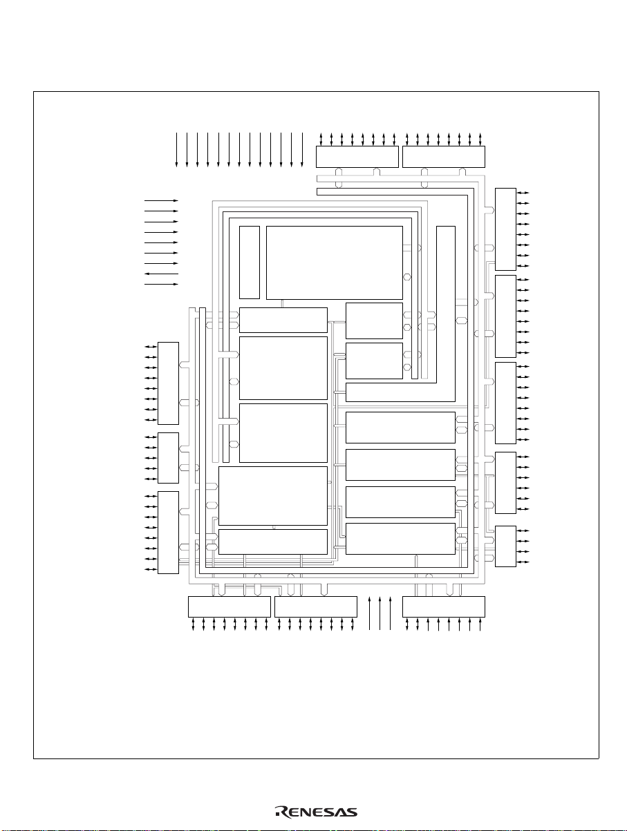
1.2 Block Diagram
y
Figure 1-1 shows an internal block diagram of the H8S/2350 Series.
15
14
13
12
11
10
9
/D
PD
8
/D
/D
/D
3
2
1
0
PD
PD
PD
VCCVCCVCCVCCVCCVSSVSSVSSVSSVSSVSSVSSV
/D
/D
/D
/D
7
6
5
PD
PD
PD
4
PD
SS
7
6
5
4
3
2
1
/D
/D
/D
/D
7
6
5
PE
PE
PE
PE
0
/D
/D
/D
/D
4
3
2
1
0
PE
PE
PE
PE
PF
/WAIT /LCAS/BREQO
2
P67/CS7/IRQ3
P6
6
P6
P6
/TEND0/CS5
P6
1
/DREQ0/CS4
P6
0
MD
MD
MD
EXTAL
XTAL
STBY
RES
WDTOVF
NMI
PF7/ø
/AS
PF
6
/RD
PF
5
/HWR
PF
4
/LWR
PF
3
/BACK
PF
1
/BREQ
PF
0
PG
/CS0
4
/CS1
PG
3
/CS2
PG
2
PG
/CS3
1
/CAS
PG
0
/CS6/IRQ2
/IRQ1
P6
5
/IRQ0
P6
4
/TEND1
3
/DREQ1
2
WDT
SCI
Port E
Internal data bus
Internal address bus
Bus controller
Peripheral data bus
Peripheral address bus
Port
Port
Port
Port
Port
A
B
C
3
5
PA
/IRQ7
7/A23
PA
/IRQ6
6/A22
/IRQ5
PA
5/A21
/IRQ4
PA
4/A20
PA
3/A19
PA2/A
18
PA1/A
17
PA0/A
16
PB7/A
15
PB6/A
14
PB5/A
13
PB4/A
12
PB3/A
11
PB2/A
10
PB1/A
9
PB0/A
8
PC7/A
7
PC6/A
6
PC5/A
5
PC4/A
4
PC3/A
3
PC2/A
2
PC1/A
1
PC0/A
0
P35/SCK1
/SCK0
P3
4
P3
/RxD1
3
/RxD0
P3
2
/TxD1
P3
1
/TxD0
P3
0
P5
0
P5
1
P5
2
P53/ADTRG
Port D
2
1
0
H8S/2000 CPU
generator
Clock pulse
Port
Interrupt controller
*
ROM
F
DTC
DMAC
RAM
Port
G
Port
TPU
6
PPG
D/A converter
A/D converter
Note: * Onl
applies to the H8S/2351.
/PO0/TIOCA3
/PO1/TIOCB3
/PO2/TIOCC3
0
/PO14/TIOCA2
6
P1
/PO15/TIOCB2/TCLKD
7
P1
1
2
P2
P2
P2
/PO8/TIOCA0/DACK0
/PO9/TIOCB0/DACK1
0
1
P1
P1
/PO10/TIOCC0/TCLKA
/PO11/TIOCD0/TCLKB
2
3
P1
P1
/PO12/TIOCA1
4
P1
/PO13/TIOCB1/TCLKC
5
P1
Figure 1-1 Block Diagram
/PO4/TIOCA4
/PO3/TIOCD3
4
3
P2
P2
/PO5/TIOCB4
/PO6/TIOCA5
5
6
P2
P2
V
/PO7/TIOCB5
7
P2
Port 4Port 2Port 1
ref
SS
CC
AV
/AN5
/AN4
/AN3
/AN2
/AN1
AV
5
P4
P4
/AN7/DA1
/AN6/DA0
7
6
P4
P4
/AN0
4
3
2
1
0
P4
P4
P4
P4
5
Page 26
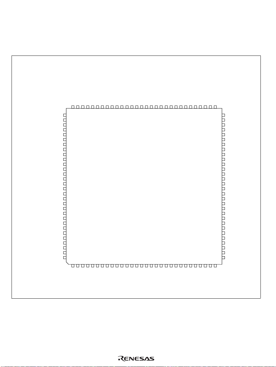
1.3 Pin Description
1.3.1 Pin Arrangement
Figures 1-2 and 1-3 show the pin arrangement of the H8S/2350 Series.
/BREQ
/BACK
/LCAS/WAIT /BREQO
/LWR
/HWR
/RD
/AS
P5
P53/ADTRG
AV
V
P40/AN0
/AN1
P4
1
P4
/AN2
2
/AN3
P4
3
/AN4
P4
4
P4
/AN5
5
/AN6/DA0
P4
6
/AN7/DA1
P4
7
AV
V
P17/PO15/TIOCB2/TCLKD
P1
/PO14/TIOCA2
6
/PO13/TIOCB1/TCLKC
P1
5
/PO12/TIOCA1
P1
P1
P1
4
/PO11/TIOCD0/TCLKB
3
/PO10/TIOCC0/TCLKA
2
/PO9/TIOCB0/DACK1
P1
1
P1
/PO8/TIOCA0/DACK0
0
MD
MD
MD
PG0/CAS
/CS3
PG
1
PG
/CS2
2
/CS1
PG
3
/CS0
PG
4
0
1
2
3
4
P51P50PF
9089888786858483828180797877767574737271706968676665646362
91
2
92
93
CC
94
ref
95
PF
PF
PF
PF
/ø
5
6
7
CC
SS
PF
EXTAL
XTAL
PF
PF
V
VCCSTBY
V
96
97
98
99
100
101
102
103
SS
104
SS
105
106
107
108
109
110
111
112
113
0
114
1
115
2
116
117
118
119
120
1234567891011121314151617181920212223242526272829
0
1
2
3
4
5
6
7
8
9
10
11
/A
PC
SS
/A
/A
/A
/A
/A
/A
/A
V
1
2
3
4
PC
PC
PC
PC
/A
5
6
7
0
1
PB
PB
PC
PC
CC
/A
V
0
PC
12
SS
V
/A
/A
/A
2
3
4
PB
PB
PB
NMI
13
/A
5
PB
RES
WDTOVF
14
/A
/A
6
PB
PB
/PO0/TIOCA3
0
P2
15
16
/A
7
0
PA
/PO1/TIOCB3
/PO2/TIOCC3
1
2
P2
P2
17
18
/A
/A
2
1
PA
PA
/PO3/TIOCD3
P2
/A
PA
/PO4/TIOCA4
3
P2
19
V
3
/PO5/TIOCB4
4
P2
SS
/IRQ4
/A
PA
/PO6/TIOCA5
5
P2
/IRQ5
20
/A
4
PA
/PO7/TIOCB5
6
P2
/IRQ6
21
/A
5
PA
7
22
6
/TEND1
/DREQ1
3
2
P6
P6
/IRQ7
23
/A
/CS7/IRQ3
7
7
PA
P6
/TEND0/CS5
1
P6
61
60
P60/DREQ0/CS4
59
V
SS
58
P35/SCK1
57
P3
P3
56
P3
55
P3
54
P3
53
V
52
CC
PD7/D
51
PD6/D
50
PD5/D
49
PD4/D
48
V
47
SS
PD3/D
46
PD2/D
45
PD1/D
44
PD0/D
43
PE7/D
42
PE6/D
41
PE5/D
40
PE4/D
39
V
38
SS
PE3/D
37
PE2/D
36
PE1/D
35
PE0/D
34
V
33
CC
P64/IRQ0
32
P6
31
30
/CS6/IRQ2
6
P6
/SCK0
4
/RxD1
3
/RxD0
2
/TxD1
1
/TxD0
0
/IRQ1
5
15
14
13
12
11
10
9
8
7
6
5
4
3
2
1
0
Figure 1-2 Pin Arrangement (TFP-120: Top View)
6
Page 27

AV
V
P40/AN0
P4
/AN1
1
P4
/AN2
2
P4
/AN3
3
P4
/AN4
4
P4
/AN5
5
P4
/AN6/DA0
6
P4
/AN7/DA1
7
AV
P17/PO15/TIOCB2/TCLKD
P1
6
P1
/PO13/TIOCB1/TCLKC
5
P1
4
P1
/PO11/TIOCD0/TCLKB
3
P1
/PO10/TIOCC0/TCLKA
2
P1
/PO9/TIOCB0/DACK1
1
P1
/PO8/TIOCA0/DACK0
0
V
/PO14/TIOCA2
/PO12/TIOCA1
MD
MD
MD
PG0/CAS
PG
/CS3
1
PG
/CS2
2
/BREQ
/BACK
/LCAS/WAIT /BREQO
/LWR
/HWR
/RD
/AS
/ø
4
5
6
7
CC
PF
4
/A
4
PC
SS
PF
PF
V
V
PF
EXTAL
XTAL
VCCSTBY
NMI
RES
5
6
7
8
9
10
11
12
13
14
/A
/A
/A
5
6
7
PC
PC
PC
SS
/A
/A
V
/A
/A
/A
/A
0
1
2
PB
PB
PB
/A
3
4
5
6
PB
PB
PB
PB
103
CC
104
ref
105
106
107
108
109
110
111
112
113
SS
114
SS
115
116
117
118
119
120
121
122
123
0
124
1
125
2
126
127
128
/ADTRG
3
2
P5
P5
102
101
123456789
/CS1
/CS0
3
4
PG
PG
0
1
2
3
PF
PF
VSSVSSP51P50PF
9998979695949392919089888786858483828180797877767574737271706968676665
100
PF
1011121314151617181920212223242526272829303132333435363738
0
1
2
SS
NC
V
3
CC
V
SS
/A
/A
/A
/A
V
0
1
2
3
PC
PC
PC
PC
Figure 1-3 Pin Arrangement (FP-128: Top View)
/PO0/TIOCA3
/PO1/TIOCB3
0
1
P2
WDTOVF
P2
15
16
17
/A
/A
/A
7
0
1
PB
PA
PA
/PO2/TIOCC3
/PO3/TIOCD3
2
3
P2
P2
18
19
/A
/A
2
3
PA
PA
/PO4/TIOCA4
/PO5/TIOCB4
4
5
P2
P2
SS
V
/IRQ4
20
/A
4
PA
/PO6/TIOCA5
/PO7/TIOCB5
6
7
P2
P2
/IRQ5
/IRQ6
21
22
/A
/A
5
6
PA
PA
/TEND1
/DREQ1
3
2
P6
P6
/IRQ7
23
/A
/CS7/IRQ3
7
7
PA
P6
/TEND0/CS5
1
P6
/CS6/IRQ2
6
P6
SSVSS
V
SSVSS
V
/DREQ0/CS4
0
P6
/IRQ1
5
P6
SS
V
64
63
62
61
60
59
58
57
56
55
54
53
52
51
50
49
48
47
46
45
44
43
42
41
40
39
/IRQ0
4
P6
P35/SCK1
P3
/SCK0
4
P3
/RxD1
3
P3
/RxD0
2
P3
/TxD1
1
P3
/TxD0
0
V
CC
PD7/D
15
PD6/D
14
PD5/D
13
PD4/D
12
V
SS
PD3/D
11
PD2/D
10
PD1/D
9
PD0/D
8
PE7/D
7
PE6/D
6
PE5/D
5
PE4/D
4
V
SS
PE3/D
3
PE2/D
2
PE1/D
1
PE0/D
0
V
CC
7
Page 28

1.3.2 Pin Functions in Each Operating Mode
Table 1-2 shows the pin functions of the H8S/2350 Series in each of the operating modes.
Table 1-2 Pin Functions in Each Operating Mode
Pin No. Pin Name
TFP-120 FP-128 Mode 1 Mode 2* Mode 3* Mode 4 Mode 5 Mode 6* Mode 7*
15 VCCV
CC
26 A0PC0/A
37 A1PC1/A
48 A2PC2/A
59 A3PC3/A
610VSSV
SS
711A4PC4/A
812A5PC5/A
913A6PC6/A
10 14 A
11 15 A
12 16 A
13 17 A
14 18 A
15 19 V
16 20 A
17 21 A
18 22 A
19 23 A
20 24 PA
21 25 PA
22 26 PA
23 27 PA
24 28 V
7
8
9
10
11
SS
12
13
14
15
0
1
2
3
SS
PC7/A
PB0/A
PB1/A
PB2/A
PB3/A
V
SS
PB4/A
PB5/A
PB6/A
PB7/A
PA
0
PA
1
PA
2
PA
3
V
SS
25 29 PA4/IRQ4 PA4/IRQ4 PA4/IRQ4 A
26 30 PA5/IRQ5 PA5/IRQ5 PA5/IRQ5 PA5/A21/
27 31 PA6/IRQ6 PA6/IRQ6 PA6/IRQ6 PA6/A22/
V
CC
PC
0
1
2
3
4
5
6
7
8
9
10
11
12
13
14
15
PC
PC
PC
V
PC
PC
PC
PC
PB
PB
PB
PB
V
PB
PB
PB
PB
PA
PA
PA
PA
V
0
1
2
3
SS
4
5
6
7
0
1
2
3
SS
4
5
6
7
0
1
2
3
SS
V
CC
A
0
A
1
A
2
A
3
V
SS
A
4
A
5
A
6
A
7
A
8
A
9
A
10
A
11
V
SS
A
12
A
13
A
14
A
15
A
16
A
17
A
18
A
19
V
SS
20
V
CC
A
0
A
1
A
2
A
3
V
SS
A
4
A
5
A
6
A
7
A
8
A
9
A
10
A
11
V
SS
A
12
A
13
A
14
A
15
A
16
A
17
A
18
A
19
V
SS
A
20
V
CC
PC0/A
0
PC1/A
1
PC2/A
2
PC3/A
3
V
SS
PC4/A
4
PC5/A
5
PC6/A
6
PC7/A
7
PB0/A
8
PB1/A
9
PB2/A
10
PB3/A
11
V
SS
PB4/A
12
PB5/A
13
PB6/A
14
PB7/A
15
PA0/A
16
PA1/A
17
PA2/A
18
PA3/A
19
V
SS
PA4/A20/
V
CC
PC
0
PC
1
PC
2
PC
3
V
SS
PC
4
PC
5
PC
6
PC
7
PB
0
PB
1
PB
2
PB
3
V
SS
PB
4
PB
5
PB
6
PB
7
PA
0
PA
1
PA
2
PA
3
V
SS
PA4/IRQ4
IRQ4
IRQ5
IRQ6
PA5/A21/
IRQ5
PA6/A22/
IRQ6
PA5/A21/
IRQ5
PA6/A22/
IRQ6
PA5/IRQ5
PA6/IRQ6
8
Page 29

Table 1-2 Pin Functions in Each Operating Mode (cont)
Pin No. Pin Name
TFP-120 FP-128 Mode 1 Mode 2* Mode 3* Mode 4 Mode 5 Mode 6* Mode 7*
28 32 PA7/IRQ7 PA7/IRQ7 PA7/IRQ7 PA7/A23/
IRQ7
29 33 P67/IRQ3 P67/IRQ3 P67/IRQ3 P67/IRQ3/
CS7
30 34 P66/IRQ2 P66/IRQ2 P66/IRQ2 P66/IRQ2/
CS6
—35 VSSV
—36 VSSV
SS
SS
V
SS
V
SS
V
SS
V
SS
31 37 P65/IRQ1 P65/IRQ1 P65/IRQ1 P65/IRQ1 P65/IRQ1 P65/IRQ1 P65/IRQ1
32 38 P64/IRQ0 P64/IRQ0 P64/IRQ0 P64/IRQ0 P64/IRQ0 P64/IRQ0 P64/IRQ0
33 39 V
CC
34 40 PE0/D
35 41 PE1/D
36 42 PE2/D
37 43 PE3/D
38 44 V
SS
39 45 PE4/D
40 46 PE5/D
41 47 PE6/D
42 48 PE7/D
43 49 D
44 50 D
45 51 D
46 52 D
47 53 V
48 54 D
49 55 D
50 56 D
51 57 D
52 58 V
8
9
10
11
SS
12
13
14
15
CC
V
CC
PE0/D
0
PE1/D
1
PE2/D
2
PE3/D
3
V
SS
PE4/D
4
PE5/D
5
PE6/D
6
PE7/D
7
D
8
D
9
D
10
D
11
V
SS
D
12
D
13
D
14
D
15
V
CC
V
CC
PE
0
1
2
3
4
5
6
7
PE
PE
PE
V
PE
PE
PE
PE
PD
PD
PD
PD
V
PD
PD
PD
PD
V
0
1
2
3
SS
4
5
6
7
0
1
2
3
SS
4
5
6
7
CC
V
CC
PE0/D
PE1/D
PE2/D
PE3/D
V
SS
PE4/D
PE5/D
PE6/D
PE7/D
D
8
D
9
D
10
D
11
V
SS
D
12
D
13
D
14
D
15
V
CC
53 59 P30/TxD0 P30/TxD0 P30/TxD0 P30/TxD0 P30/TxD0 P30/TxD0 P30/TxD0
54 60 P31/TxD1 P31/TxD1 P31/TxD1 P31/TxD1 P31/TxD1 P31/TxD1 P31/TxD1
55 61 P32/RxD0 P32/RxD0 P32/RxD0 P32/RxD0 P32/RxD0 P32/RxD0 P32/RxD0
0
1
2
3
4
5
6
7
PA7/A23/
IRQ7
P67/IRQ3/
CS7
P66/IRQ2/
CS6
V
SS
V
SS
V
CC
PE0/D
0
PE1/D
1
PE2/D
2
PE3/D
3
V
SS
PE4/D
4
PE5/D
5
PE6/D
6
PE7/D
7
D
8
D
9
D
10
D
11
V
SS
D
12
D
13
D
14
D
15
V
CC
PA7/A23/
IRQ7
P67/IRQ3/
CS7
P66/IRQ2/
CS6
V
SS
V
SS
V
CC
PE0/D
0
PE1/D
1
PE2/D
2
PE3/D
3
V
SS
PE4/D
4
PE5/D
5
PE6/D
6
PE7/D
7
D
8
D
9
D
10
D
11
V
SS
D
12
D
13
D
14
D
15
V
CC
PA7/IRQ7
P67/IRQ3
P66/IRQ2
V
SS
V
SS
V
CC
PE
0
PE
1
PE
2
PE
3
V
SS
PE
4
PE
5
PE
6
PE
7
PD
0
PD
1
PD
2
PD
3
V
SS
PD
4
PD
5
PD
6
PD
7
V
CC
9
Page 30

Table 1-2 Pin Functions in Each Operating Mode (cont)
Pin No. Pin Name
TFP-120 FP-128 Mode 1 Mode 2* Mode 3* Mode 4 Mode 5 Mode 6* Mode 7*
56 62 P33/RxD1 P33/RxD1 P33/RxD1 P33/RxD1 P33/RxD1 P33/RxD1 P33/RxD1
57 63 P34/SCK0 P34/SCK0 P34/SCK0 P34/SCK0 P34/SCK0 P34/SCK0 P34/SCK0
58 64 P35/SCK1 P35/SCK1 P35/SCK1 P35/SCK1 P35/SCK1 P35/SCK1 P35/SCK1
59 65 V
SS
60 66 P60/
DREQ0
—67 VSSV
—68 VSSV
61 69 P61/
TEND0
62 70 P62/
DREQ1
63 71 P63/
TEND1
64 72 P27/PO7/
TIOCB5
65 73 P26/PO6/
TIOCA5
66 74 P25/PO5/
TIOCB4
67 75 P24/PO4/
TIOCA4
68 76 P23/PO3/
TIOCD3
69 77 P22/PO2/
TIOCC3
70 78 P21/PO1/
TIOCB3
71 79 P20/PO0/
TIOCA3
72 80 WDTOVF WDTOVF WDTOVF WDTOVF WDTOVF WDTOVF WDTOVF
73 81 RES RES RES RES RES RES RES
74 82 NMI NMI NMI NMI NMI NMI NMI
V
SS
P60/
DREQ0
SS
SS
P61/
TEND0
P62/
DREQ1
P63/
TEND1
P27/PO7/
TIOCB5
P26/PO6/
TIOCA5
P25/PO5/
TIOCB4
P24/PO4/
TIOCA4
P23/PO3/
TIOCD3
P22/PO2/
TIOCC3
P21/PO1/
TIOCB3
P20/PO0/
TIOCA3
V
SS
P60/
DREQ0
V
SS
V
SS
P61/
TEND0
P62/
DREQ1
P63/
TEND1
P27/PO7/
TIOCB5
P26/PO6/
TIOCA5
P25/PO5/
TIOCB4
P24/PO4/
TIOCA4
P23/PO3/
TIOCD3
P22/PO2/
TIOCC3
P21/PO1/
TIOCB3
P20/PO0/
TIOCA3
V
SS
P60/
DREQ0/
CS4
V
SS
V
SS
P61/
TEND0/
CS5
P62/
DREQ1
P63/
TEND1
P27/PO7/
TIOCB5
P26/PO6/
TIOCA5
P25/PO5/
TIOCB4
P24/PO4/
TIOCA4
P23/PO3/
TIOCD3
P22/PO2/
TIOCC3
P21/PO1/
TIOCB3
P20/PO0/
TIOCA3
V
SS
P60/
DREQ0/
CS4
V
SS
V
SS
P61/
TEND0/
CS5
P62/
DREQ1
P63/
TEND1
P27/PO7/
TIOCB5
P26/PO6/
TIOCA5
P25/PO5/
TIOCB4
P24/PO4/
TIOCA4
P23/PO3/
TIOCD3
P22/PO2/
TIOCC3
P21/PO1/
TIOCB3
P20/PO0/
TIOCA3
V
SS
P60/
DREQ0/
CS4
V
SS
V
SS
P61/
TEND0/
CS5
P62/
DREQ1
P63/
TEND1
P27/PO7/
TIOCB5
P26/PO6/
TIOCA5
P25/PO5/
TIOCB4
P24/PO4/
TIOCA4
P23/PO3/
TIOCD3
P22/PO2/
TIOCC3
P21/PO1/
TIOCB3
P20/PO0/
TIOCA3
V
SS
P60/
DREQ0
V
SS
V
SS
P61/
TEND0
P62/
DREQ1
P63/
TEND1
P27/PO7/
TIOCB5
P26/PO6/
TIOCA5
P25/PO5/
TIOCB4
P24/PO4/
TIOCA4
P23/PO3/
TIOCD3
P22/PO2/
TIOCC3
P21/PO1/
TIOCB3
P20/PO0/
TIOCA3
10
Page 31

Table 1-2 Pin Functions in Each Operating Mode (cont)
Pin No. Pin Name
TFP-120 FP-128 Mode 1 Mode 2* Mode 3* Mode 4 Mode 5 Mode 6* Mode 7*
75 83 STBY STBY STBY STBY STBY STBY STBY
76 84 V
CC
77 85 XTAL XTAL XTAL XTAL XTAL XTAL XTAL
78 86 EXTAL EXTAL EXTAL EXTAL EXTAL EXTAL EXTAL
79 87 V
SS
80 88 PF7/ø PF7/ø PF7/ø PF7/ø PF7/ø PF7/ø PF7/ø
81 89 V
CC
82 90 AS AS PF
83 91 RD RD PF
84 92 HWR HWR PF
85 93 LWR LWR PF
86 94 PF2/WAIT/
BREQO
87 95 PF1/BACK PF1/BACK PF
88 96 PF0/BREQ PF0/BREQ PF
89 97 P5
90 98 P5
0
1
—99 VSSV
— 100 V
91 101 P5
SS
2
92 102 P53/
ADTRG
93 103 AV
94 104 V
CC
ref
95 105 P40/AN0 P40/AN0 P40/AN0 P40/AN0 P40/AN0 P40/AN0 P40/AN0
96 106 P41/AN1 P41/AN1 P41/AN1 P41/AN1 P41/AN1 P41/AN1 P41/AN1
97 107 P42/AN2 P42/AN2 P42/AN2 P42/AN2 P42/AN2 P42/AN2 P42/AN2
98 108 P43/AN3 P43/AN3 P43/AN3 P43/AN3 P43/AN3 P43/AN3 P43/AN3
99 109 P44/AN4 P44/AN4 P44/AN4 P44/AN4 P44/AN4 P44/AN4 P44/AN4
100 110 P45/AN5 P45/AN5 P45/AN5 P45/AN5 P45/AN5 P45/AN5 P45/AN5
101 111 P46/AN6/
DA0
V
CC
V
SS
V
CC
PF2/WAIT/
BREQO
P5
0
P5
1
SS
V
SS
P5
2
P53/
ADTRG
AV
CC
V
ref
P46/AN6/
DA0
V
CC
V
SS
V
CC
6
5
4
3
PF
2
1
0
P5
0
P5
1
V
SS
V
SS
P5
2
P53/
ADTRG
AV
CC
V
ref
P46/AN6/
DA0
V
CC
V
SS
V
CC
V
CC
V
SS
V
CC
V
CC
V
SS
V
CC
V
V
V
AS AS AS PF
RD RD RD PF
HWR HWR HWR PF
LWR LWR LWR PF
PF2/LCAS/
WAIT/
BREQO
PF2/LCAS/
WAIT/
BREQO
PF2/LCAS/
WAIT/
BREQO
PF
PF1/BACK PF1/BACK PF1/BACK PF
PF0/BREQ PF0/BREQ PF0/BREQ PF
P5
0
P5
1
V
SS
V
SS
P5
2
P53/
ADTRG
AV
CC
V
ref
P46/AN6/
DA0
P5
0
P5
1
V
SS
V
SS
P5
2
P53/
ADTRG
AV
CC
V
ref
P46/AN6/
DA0
P5
0
P5
1
V
SS
V
SS
P5
2
P53/
ADTRG
AV
CC
V
ref
P46/AN6/
DA0
P5
P5
V
V
P5
P53/
ADTRG
AV
V
P46/AN6/
DA0
CC
SS
CC
6
5
4
3
2
1
0
0
1
SS
SS
2
CC
ref
11
Page 32

Table 1-2 Pin Functions in Each Operating Mode (cont)
Pin No. Pin Name
TFP-120 FP-128 Mode 1 Mode 2* Mode 3* Mode 4 Mode 5 Mode 6* Mode 7*
102 112 P47/AN7/
DA1
103 113 AV
104 114 V
SS
SS
105 115 P17/PO15/
TIOCB2/
TCLKD
106 116 P16/PO14/
TIOCA2
107 117 P15/PO13/
TIOCB1/
TCLKC
108 118 P14/PO12/
TIOCA1
109 119 P13/PO11/
TIOCD0/
TCLKB
110 120 P12/PO10/
TIOCC0/
TCLKA
111 121 P11/PO9/
TIOCB0/
DACK1
112 122 P10/PO8/
TIOCA0/
DACK0
113 123 MD
114 124 MD
115 125 MD
116 126 PG
117 127 PG
118 128 PG
119 1 PG
0
1
2
0
1
2
3
120 2 PG4/CS0 PG4/CS0 PG
—3 VSSV
— 4 NC NC NC NC NC NC NC
Note: NC pins should be connected to VSS or left open.
* Only applies to the H8S/2351.
P47/AN7/
DA1
AV
SS
V
SS
P17/PO15/
TIOCB2/
TCLKD
P16/PO14/
TIOCA2
P15/PO13/
TIOCB1/
TCLKC
P14/PO12/
TIOCA1
P13/PO11/
TIOCD0/
TCLKB
P12/PO10/
TIOCC0/
TCLKA
P11/PO9/
TIOCB0/
DACK1
P10/PO8/
TIOCA0/
DACK0
MD
0
MD
1
MD
2
PG
0
PG
1
PG
2
PG
3
SS
P47/AN7/
DA1
AV
SS
V
SS
P17/PO15/
TIOCB2/
TCLKD
P16/PO14/
TIOCA2
P15/PO13/
TIOCB1/
TCLKC
P14/PO12/
TIOCA1
P13/PO11/
TIOCD0/
TCLKB
P12/PO10/
TIOCC0/
TCLKA
P11/PO9/
TIOCB0/
DACK1
P10/PO8/
TIOCA0/
DACK0
MD
0
MD
1
MD
2
PG
0
PG
1
PG
2
PG
3
4
V
SS
P47/AN7/
DA1
AV
SS
V
SS
P17/PO15/
TIOCB2/
TCLKD
P16/PO14/
TIOCA2
P15/PO13/
TIOCB1/
TCLKC
P14/PO12/
TIOCA1
P13/PO11/
TIOCD0/
TCLKB
P12/PO10/
TIOCC0/
TCLKA
P11/PO9/
TIOCB0/
DACK1
P10/PO8/
TIOCA0/
DACK0
MD
0
MD
1
MD
2
P47/AN7/
DA1
AV
SS
V
SS
P17/PO15/
TIOCB2/
TCLKD
P16/PO14/
TIOCA2
P15/PO13/
TIOCB1/
TCLKC
P14/PO12/
TIOCA1
P13/PO11/
TIOCD0/
TCLKB
P12/PO10/
TIOCC0/
TCLKA
P11/PO9/
TIOCB0/
DACK1
P10/PO8/
TIOCA0/
DACK0
MD
0
MD
1
MD
2
P47/AN7/
DA1
AV
SS
V
SS
P17/PO15/
TIOCB2/
TCLKD
P16/PO14/
TIOCA2
P15/PO13/
TIOCB1/
TCLKC
P14/PO12/
TIOCA1
P13/PO11/
TIOCD0/
TCLKB
P12/PO10/
TIOCC0/
TCLKA
P11/PO9/
TIOCB0/
DACK1
P10/PO8/
TIOCA0/
DACK0
MD
0
MD
1
MD
2
P47/AN7/
DA1
AV
V
P17/PO15/
TIOCB2/
TCLKD
P16/PO14/
TIOCA2
P15/PO13/
TIOCB1/
TCLKC
P14/PO12/
TIOCA1
P13/PO11/
TIOCD0/
TCLKB
P12/PO10/
TIOCC0/
TCLKA
P11/PO9/
TIOCB0/
DACK1
P10/PO8/
TIOCA0/
DACK0
MD
MD
MD
PG0/CAS PG0/CAS PG0/CAS PG
PG1/CS3 PG1/CS3 PG1/CS3 PG
PG2/CS2 PG2/CS2 PG2/CS2 PG
PG3/CS1 PG3/CS1 PG3/CS1 PG
PG4/CS0 PG4/CS0 PG4/CS0 PG
V
SS
V
SS
V
SS
V
SS
SS
0
1
2
0
1
2
3
4
SS
12
Page 33

1.3.3 Pin Functions
Table 1-3 outlines the pin functions of the H8S/2350 Series.
Table 1-3 Pin Functions
Pin No.
Type Symbol TFP-120 FP-128 I/O Name and Function
Power V
CC
V
SS
Clock XTAL 77 85 Input Connects to a crystal oscillator.
EXTAL 78 86 Input Connects to a crystal oscillator.
ø 80 88 Output System clock: Supplies the system
1, 33,
52, 76,
81
6, 15,
24, 38,
47, 59,
79, 104
5, 39,
58, 84,
89
3, 10,
19, 28,
35, 36,
44, 53,
65, 67,
68, 87,
99, 100,
114
Input Power supply: For connection to the
power supply. All V
pins should be
CC
connected to the system power
supply.
Input Ground: For connection to ground
(0 V). All V
pins should be
SS
connected to the system power
supply (0 V).
See section 19, Clock Pulse
Generator, for typical connection
diagrams for a crystal oscillator and
external clock input.
The EXTAL pin can also input an
external clock.
See section 19, Clock Pulse
Generator, for typical connection
diagrams for a crystal oscillator and
external clock input.
clock to an external device.
13
Page 34

Table 1-3 Pin Functions (cont)
Pin No.
Type Symbol TFP-120 FP-128 I/O Name and Function
Operating mode
control
System control RES 73 81 Input Reset input: When this pin is driven
MD2 to
MD
0
115 to
113
125 to
123
Input Mode pins: These pins set the
operating mode.
The relation between the settings of
pins MD
to MD0 and the operating
2
mode is shown below. These pins
should not be changed while the
H8S/2350 Series is operating.
Operating
MD2 MD1 MD0
Mode
000—
1 Mode 1
1 0 Mode 2*
1 Mode 3*
1 0 0 Mode 4
1 Mode 5
1 0 Mode 6*
1 Mode 7*
Note: *Only applies to the H8S/2351.
low, the chip is reset. The type of
reset can be selected according to
the NMI input level. At power-on, the
NMI pin input level should be set
high.
STBY 75 83 Input Standby: When this pin is driven low,
a transition is made to hardware
standby mode.
BREQ 88 96 Input Bus request: Used by an external bus
master to issue a bus request to the
H8S/2350 Series.
BREQO 86 94 Output Bus request output: The external bus
request signal used when an internal
bus master accesses external space
in the external bus-released state.
BACK 87 95 Output Bus request acknowledge: Indicates
that the bus has been released to an
external bus master.
14
Page 35

Table 1-3 Pin Functions (cont)
Pin No.
Type Symbol TFP-120 FP-128 I/O Name and Function
Interrupts NMI 74 82 Input Nonmaskable interrupt: Requests a
nonmaskable interrupt. When this pin
is not used, it should be fixed high.
IRQ7 to
IRQ0
Address bus A23 to
A
0
Data bus D15 to
D
0
Bus control CS7 to
CS0
AS 82 90 Output Address strobe: When this pin is low,
RD 83 91 Output Read: When this pin is low, it
HWR 84 92 Output High write/write enable:
LWR 85 93 Output Low write:
CAS 116 126 Output Upper column address strobe/column
28 to 25,
29 to 32
28 to 25,
23 to 16,
14 to 7,
5 to 2
51 to 48,
46 to 39,
37 to 34
29, 30,
61, 60,
117 to 120
32 to 29,
33, 34,
37, 38
32 to 29,
27 to 20,
18 to 11,
9 to 6
57 to 54,
52 to 45,
43 to 40
33, 34,
69, 66,
127, 128,
1, 2
Input Interrupt request 7 to 0: These pins
request a maskable interrupt.
Output Address bus: These pins output an
address.
I/O Data bus: These pins constitute a
bidirectional data bus.
Output Chip select: Signals for selecting
areas 7 to 0.
it indicates that address output on the
address bus is enabled.
indicates that the external address
space can be read.
A strobe signal that writes to external
space and indicates that the upper
half (D
to D8) of the data bus is
15
enabled.
The 2CAS type DRAM write enable
signal.
A strobe signal that writes to external
space and indicates that the lower
half (D
to D0) of the data bus is
7
enabled.
address strobe:
The 2CAS type DRAM upper column
address strobe signal.
15
Page 36

Table 1-3 Pin Functions (cont)
Pin No.
Type Symbol TFP-120 FP-128 I/O Name and Function
Bus control WAIT 86 94 Input Wait: Requests insertion of a wait
state in the bus cycle when
accessing external 3-state address
space.
LCAS 86 94 Output Lower column address strobe: The 2-
CAS type DRAM lower column
address strobe signal
DMA controller
(DMAC)
16-bit timerpulse unit
(TPU)
DREQ1,
DREQ0
TEND1,
TEND0
DACK1,
DACK0
TCLKD to
TCLKA
TIOCA0,
TIOCB0,
TIOCC0,
TIOCD0
TIOCA1,
TIOCB1
TIOCA2,
TIOCB2
TIOCA3,
TIOCB3,
TIOCC3,
TIOCD3
62, 60 70, 66 Input DMA request 1 and 0: These pins
request DMAC activation.
63, 61 71, 69 Output DMA transfer end 1 and 0: These
pins indicate the end of DMAC data
transfer.
111, 112 121, 122 Output DMA transfer acknowledge 1 and 0:
These are the DMAC single address
transfer acknowledge pins.
105, 107,
109, 110
112 to
109
108, 107 118, 117 I/O Input capture/ output compare match
106, 105 116, 115 I/O Input capture/ output compare match
71 to 68 79 to 76 I/O Input capture/ output compare match
115, 117,
119, 120
122 to
119
Input Clock input D to A: These pins input
an external clock.
I/O Input capture/ output compare match
A0 to D0: The TGR0A to TGR0D
input capture input or output compare
output, or PWM output pins.
A1 and B1: The TGR1A and TGR1B
input capture input or output compare
output, or PWM output pins.
A2 and B2: The TGR2A and TGR2B
input capture input or output compare
output, or PWM output pins.
A3 to D3: The TGR3A to TGR3D
input capture input or output compare
output, or PWM output pins.
16
Page 37

Table 1-3 Pin Functions (cont)
Pin No.
Type Symbol TFP-120 FP-128 I/O Name and Function
16-bit timerpulse unit
(TPU)
Programmable
pulse generator
(PPG)
Watchdog
timer (WDT)
Serial
communication
interface (SCI)
Smart Card
interface
A/D converter AN7 to
D/A converter DA1, DA0 102, 101 112, 111 Output Analog output: D/A converter analog
TIOCA4,
TIOCB4
TIOCA5,
TIOCB5
PO15 to
PO0
WDTOVF 72 80 Output Watchdog timer overflows: The
TxD1,
TxD0
RxD1,
RxD0
SCK1,
SCK0
AN0
ADTRG 92 102 Input A/D conversion external trigger input:
67, 66 75, 74 I/O Input capture/ output compare match
A4 and B4: The TGR4A and TGR4B
input capture input or output compare
output, or PWM output pins.
65, 64 73, 72 I/O Input capture/ output compare match
A5 and B5: The TGR5A and TGR5B
input capture input or output compare
output, or PWM output pins.
105 to
112,
64 to 71
54, 53 60, 59 Output Transmit data (channel 0, 1):
56, 55 62, 61 Input Receive data (channel 0, 1):
58, 57 64, 63 I/O Serial clock (channel 0, 1):
102 to95112 to
115 to
122,
72 to 79
105
Output Pulse output 15 to 0: Pulse output
pins.
counter overflows signal output pin in
watchdog timer mode.
Data output pins.
Data input pins.
Clock I/O pins.
Input Analog 7 to 0: Analog input pins.
Pin for input of an external trigger to
start A/D conversion.
output pins.
17
Page 38

Table 1-3 Pin Functions (cont)
Pin No.
Type Symbol TFP-120 FP-128 I/O Name and Function
A/D converter
and D/A
converter
I/O ports P17 to
AV
CC
AV
SS
V
ref
P1
0
P27 to
P2
0
P35 to
P3
0
P47 to
P4
0
P53 to
P5
0
93 103 Input This is the power supply pin for the
A/D converter and D/A converter.
When the A/D converter and D/A
converter are not used, this pin
should be connected to the system
power supply (+5 V).
103 113 Input This is the ground pin for the A/D
converter and D/A converter.
This pin should be connected to the
system power supply (0 V).
94 104 Input This is the reference voltage input pin
for the A/D converter and D/A
converter.
When the A/D converter and D/A
converter are not used, this pin
should be connected to the system
power supply (+5 V).
105 to
112
115 to
122
I/O Port 1: An 8-bit I/O port. Input or
output can be designated for each bit
by means of the port 1 data direction
register (P1DDR).
64 to 71 72 to 79 I/O Port 2: An 8-bit I/O port. Input or
output can be designated for each bit
by means of the port 2 data direction
register (P2DDR).
58 to 53 64 to 59 I/O Port 3: A 6-bit I/O port. Input or
output can be designated for each bit
by means of the port 3 data direction
register (P3DDR).
102 to
95
92 to 89 102, 101,
112 to
105
98, 97
Input Port 4: An 8-bit input port.
I/O Port 5: A 4-bit I/O port. Input or
output can be designated for each bit
by means of the port 5 data direction
register (P5DDR).
18
Page 39

Table 1-3 Pin Functions (cont)
Pin No.
Type Symbol TFP-120 FP-128 I/O Name and Function
I/O ports P67 to
P6
0
PA7 to
PA
0
PB7 to
PB
0
PC7 to
PC
0
PD7 to
PD
0
PE7 to
PE
0
PF7 to
PF
0
PG4 to
PG
0
29 to 32,
63 to 60
28 to 25,
23 to 20
19 to 16,
14 to 11
10 to 7,
5 to 2
51 to 48,
46 to 43
42 to 39,
37 to 34
80,
82 to 88
120 to
116
Note: *Only applies to the H8S/2351.
33, 34,
37, 38,
71 to 69,
66
32 to 29,
27 to 24
23 to 20,
18 to 15
14 to 11,
9 to 6
57 to 54,
52 to 49
48 to 45,
43 to 40
88,
90 to 96
2, 1,
128 to
126
I/O Port 6: An 8-bit I/O port. Input or
output can be designated for each bit
by means of the port 6 data direction
register (P6DDR).
I/O Port A: An 8-bit I/O port. Input or
output can be designated for each bit
by means of the port A data direction
register (PADDR).
I/O Port B*: An 8-bit I/O port. Input or
output can be designated for each bit
by means of the port B data direction
register (PBDDR).
I/O Port C*: An 8-bit I/O port. Input or
output can be designated for each bit
by means of the port C data direction
register (PCDDR).
I/O Port D*: An 8-bit I/O port. Input or
output can be designated for each bit
by means of the port D data direction
register (PDDDR).
I/O Port E: An 8-bit I/O port. Input or
output can be designated for each bit
by means of the port E data direction
register (PEDDR).
I/O Port F: An 8-bit I/O port. Input or
output can be designated for each bit
by means of the port F data direction
register (PFDDR).
I/O Port G: A 5-bit I/O port. Input or
output can be designated for each bit
by means of the port G data direction
register (PGDDR).
19
Page 40

20
Page 41

Section 2 CPU
2.1 Overview
The H8S/2000 CPU is a high-speed central processing unit with an internal 32-bit architecture that
is upward-compatible with the H8/300 and H8/300H CPUs. The H8S/2000 CPU has sixteen 16-bit
general registers, can address a 16-Mbyte (architecturally 4-Gbyte) linear address space, and is
ideal for realtime control.
2.1.1 Features
The H8S/2000 CPU has the following features.
• Upward-compatible with H8/300 and H8/300H CPUs
Can execute H8/300 and H8/300H object programs
• General-register architecture
Sixteen 16-bit general registers (also usable as sixteen 8-bit registers or eight 32-bit
registers)
• Sixty-five basic instructions
8/16/32-bit arithmetic and logic instructions
Multiply and divide instructions
Powerful bit-manipulation instructions
• Eight addressing modes
Register direct [Rn]
Register indirect [@ERn]
Register indirect with displacement [@(d:16,ERn) or @(d:32,ERn)]
Register indirect with post-increment or pre-decrement [@ERn+ or @–ERn]
Absolute address [@aa:8, @aa:16, @aa:24, or @aa:32]
Immediate [#xx:8, #xx:16, or #xx:32]
Program-counter relative [@(d:8,PC) or @(d:16,PC)]
Memory indirect [@@aa:8]
• 16-Mbyte address space
Program: 16 Mbytes
Data: 16 Mbytes (4 Gbytes architecturally)
21
Page 42

• High-speed operation
All frequently-used instructions execute in one or two states
Maximum clock rate : 20 MHz
8/16/32-bit register-register add/subtract : 50 ns
8 × 8-bit register-register multiply : 600 ns
16 ÷ 8-bit register-register divide : 600 ns
16 × 16-bit register-register multiply : 1000 ns
32 ÷ 16-bit register-register divide : 1000 ns
• Two CPU operating modes
Normal mode
Advanced mode
• Power-down state
Transition to power-down state by SLEEP instruction
CPU clock speed selection
2.1.2 Differences between H8S/2600 CPU and H8S/2000 CPU
The differences between the H8S/2600 CPU and the H8S/2000 CPU are as shown below.
• Register configuration
The MAC register is supported only by the H8S/2600 CPU.
• Basic instructions
The four instructions MAC, CLRMAC, LDMAC, and STMAC are supported only by the
H8S/2600 CPU.
• Number of execution states
The number of exection states of the MULXU and MULXS instructions.
Internal Operation
Instruction Mnemonic H8S/2600 H8S/2000
MULXU MULXU.B Rs, Rd 3 12
MULXU.W Rs, ERd 4 20
MULXS MULXS.B Rs, Rd 4 13
MULXS.W Rs, ERd 5 21
There are also differences in the address space, CCR and EXR functions, power-down state, etc.,
depending on the product.
22
Page 43

2.1.3 Differences from H8/300 CPU
In comparison to the H8/300 CPU, the H8S/2000 CPU has the following enhancements.
• More general registers and control registers
Eight 16-bit expanded registers, and one 8-bit control register, have been added.
• Expanded address space
Normal mode supports the same 64-kbyte address space as the H8/300 CPU.
Advanced mode supports a maximum 16-Mbyte address space.
• Enhanced addressing
The addressing modes have been enhanced to make effective use of the 16-Mbyte address
space.
• Enhanced instructions
Addressing modes of bit-manipulation instructions have been enhanced.
Signed multiply and divide instructions have been added.
Two-bit shift instructions have been added.
Instructions for saving and restoring multiple registers have been added.
A test and set instruction has been added.
• Higher speed
Basic instructions execute twice as fast.
2.1.4 Differences from H8/300H CPU
In comparison to the H8/300H CPU, the H8S/2000 CPU has the following enhancements.
• Additional control register
One 8-bit control register has been added.
• Enhanced instructions
Addressing modes of bit-manipulation instructions have been enhanced.
Two-bit shift instructions have been added.
Instructions for saving and restoring multiple registers have been added.
A test and set instruction has been added.
• Higher speed
Basic instructions execute twice as fast.
23
Page 44

2.2 CPU Operating Modes
The H8S/2000 CPU has two operating modes: normal and advanced. Normal mode supports a
maximum 64-kbyte address space. Advanced mode supports a maximum 16-Mbyte total address
space (architecturally a maximum 16-Mbyte program area and a maximum of 4 Gbytes for
program and data areas combined). The mode is selected by the mode pins of the microcontroller.
Normal mode
CPU operating modes
Advanced mode
Maximum 64 kbytes, program
and data areas combined
Maximum 16-Mbytes for
program and data areas
combined
Figure 2-1 CPU Operating Modes
(1) Normal Mode
The exception vector table and stack have the same structure as in the H8/300 CPU.
Address Space: A maximum address space of 64 kbytes can be accessed.
Extended Registers (En): The extended registers (E0 to E7) can be used as 16-bit registers, or as
the upper 16-bit segments of 32-bit registers. When En is used as a 16-bit register it can contain
any value, even when the corresponding general register (Rn) is used as an address register. If the
general register is referenced in the register indirect addressing mode with pre-decrement (@–Rn)
or post-increment (@Rn+) and a carry or borrow occurs, however, the value in the corresponding
extended register (En) will be affected.
Instruction Set: All instructions and addressing modes can be used. Only the lower 16 bits of
effective addresses (EA) are valid.
24
Page 45

Exception Vector Table and Memory Indirect Branch Addresses: In normal mode the top area
starting at H'0000 is allocated to the exception vector table. One branch address is stored per 16
bits. The configuration of the exception vector table in normal mode is shown in figure 2-2. For
details of the exception vector table, see section 4, Exception Handling.
H'0000
H'0001
H'0002
H'0003
H'0004
H'0005
H'0006
H'0007
H'0008
H'0009
H'000A
H'000B
Power-on reset exception vector
Manual reset exception vector
(Reserved for system use)
Exception vector 1
Exception vector 2
Exception
vector table
Figure 2-2 Exception Vector Table (Normal Mode)
The memory indirect addressing mode (@@aa:8) employed in the JMP and JSR instructions uses
an 8-bit absolute address included in the instruction code to specify a memory operand that
contains a branch address. In normal mode the operand is a 16-bit word operand, providing a 16bit branch address. Branch addresses can be stored in the top area from H'0000 to H'00FF. Note
that this area is also used for the exception vector table.
25
Page 46

Stack Structure: When the program counter (PC) is pushed onto the stack in a subroutine call,
and the PC, condition-code register (CCR), and extended control register (EXR) are pushed onto
the stack in exception handling, they are stored as shown in figure 2-3. When EXR is invalid, it is
not pushed onto the stack. For details, see section 4, Exception Handling.
SP
Notes: 1.
PC
(16 bits)
(a) Subroutine Branch (b) Exception Handling
When EXR is not used it is not stored on the stack.
2.
SP when EXR is not used.
3.
Ignored when returning.
SP
*2
(SP )
Reserved
*1
EXR
CCR
*3
CCR
PC
(16 bits)
*1,*3
Figure 2-3 Stack Structure in Normal Mode
(2) Advanced Mode
Address Space: Linear access is provided to a 16-Mbyte maximum address space (architecturally
a maximum 16-Mbyte program area and a maximum 4-Gbyte data area, with a maximum of 4
Gbytes for program and data areas combined).
Extended Registers (En): The extended registers (E0 to E7) can be used as 16-bit registers, or as
the upper 16-bit segments of 32-bit registers or address registers.
Instruction Set: All instructions and addressing modes can be used.
26
Page 47

Exception Vector Table and Memory Indirect Branch Addresses: In advanced mode the top
area starting at H'00000000 is allocated to the exception vector table in units of 32 bits. In each 32
bits, the upper 8 bits are ignored and a branch address is stored in the lower 24 bits (figure 2-4).
For details of the exception vector table, see section 4, Exception Handling.
H'00000000
H'00000003
H'00000004
H'00000007
H'00000008
H'0000000B
H'0000000C
H'00000010
Reserved
Power-on reset exception vector
Reserved
Manual reset exception vector
Exception vector table
(Reserved for system use)
Reserved
Exception vector 1
Figure 2-4 Exception Vector Table (Advanced Mode)
The memory indirect addressing mode (@@aa:8) employed in the JMP and JSR instructions uses
an 8-bit absolute address included in the instruction code to specify a memory operand that
contains a branch address. In advanced mode the operand is a 32-bit longword operand, providing
a 32-bit branch address. The upper 8 bits of these 32 bits are a reserved area that is regarded as
H'00. Branch addresses can be stored in the area from H'00000000 to H'000000FF. Note that the
first part of this range is also the exception vector table.
27
Page 48

Stack Structure: In advanced mode, when the program counter (PC) is pushed onto the stack in a
subroutine call, and the PC, condition-code register (CCR), and extended control register (EXR)
are pushed onto the stack in exception handling, they are stored as shown in figure 2-5. When
EXR is invalid, it is not pushed onto the stack. For details, see section 4, Exception Handling.
SP
Notes: 1.
EXR
CCR
PC
*1
*1,*3
Reserved
PC
(24 bits)
SP
*2
(SP )
Reserved
(24 bits)
(a) Subroutine Branch (b) Exception Handling
When EXR is not used it is not stored on the stack.
2.
SP when EXR is not used.
3.
Ignored when returning.
Figure 2-5 Stack Structure in Advanced Mode
28
Page 49

2.3 Address Space
Figure 2-6 shows a memory map of the H8S/2000 CPU. The H8S/2000 CPU provides linear
access to a maximum 64-kbyte address space in normal mode, and a maximum 16-Mbyte
(architecturally 4-Gbyte) address space in advanced mode.
H'0000
H'FFFF
(a) Normal Mode
H'00000000
H'00FFFFFF
Cannot be
used by the
H8S/2350
Series
H'FFFFFFFF
(b) Advanced Mode
Figure 2-6 Memory Map
Program area
Data area
29
Page 50

2.4 Register Configuration
2.4.1 Overview
The CPU has the internal registers shown in figure 2-7. There are two types of registers: general
registers and control registers.
General Registers (Rn) and Extended Registers (En)
15 07 07 0
ER0
ER1
ER2
ER3
ER4
ER5
ER6
ER7 (SP)
Control Registers (CR)
E0
E1
E2
E3
E4
E5
E6
E7
23 0
R0H
R1H
R2H
R3H
R4H
R5H
R6H
R7H
PC
R0L
R1L
R2L
R3L
R4L
R5L
R6L
R7L
Legend
SP:
PC:
EXR:
T:
I2 to I0:
CCR:
I:
UI:
Note: * In the H8S/2350 Series, this bit cannot be used as an interrupt mask.
Stack pointer
Program counter
Extended control register
Trace bit
Interrupt mask bits
Condition-code register
Interrupt mask bit
User bit or interrupt mask bit*
H:
U:
N:
Z:
V:
C:
Half-carry flag
User bit
Negative flag
Zero flag
Overflow flag
Carry flag
Figure 2-7 CPU Registers
30
76543210
T
————
76543210
IUIHUNZVCCCR
I2 I1 I0EXR
Page 51

2.4.2 General Registers
The CPU has eight 32-bit general registers. These general registers are all functionally alike and
can be used as both address registers and data registers. When a general register is used as a data
register, it can be accessed as a 32-bit, 16-bit, or 8-bit register. When the general registers are used
as 32-bit registers or address registers, they are designated by the letters ER (ER0 to ER7).
The ER registers divide into 16-bit general registers designated by the letters E (E0 to E7) and R
(R0 to R7). These registers are functionally equivalent, providing a maximum sixteen 16-bit
registers. The E registers (E0 to E7) are also referred to as extended registers.
The R registers divide into 8-bit general registers designated by the letters RH (R0H to R7H) and
RL (R0L to R7L). These registers are functionally equivalent, providing a maximum sixteen 8-bit
registers.
Figure 2-8 illustrates the usage of the general registers. The usage of each register can be selected
independently.
• Address registers
• 32-bit registers • 16-bit registers • 8-bit registers
E registers (extended registers)
(E0 to E7)
ER registers
(ER0 to ER7)
R registers
(R0 to R7)
RH registers
(R0H to R7H)
RL registers
(R0L to R7L)
Figure 2-8 Usage of General Registers
31
Page 52

General register ER7 has the function of stack pointer (SP) in addition to its general-register
function, and is used implicitly in exception handling and subroutine calls. Figure 2-9 shows the
stack.
Free area
SP (ER7)
Stack area
Figure 2-9 Stack
2.4.3 Control Registers
The control registers are the 24-bit program counter (PC), 8-bit extended control register (EXR),
and 8-bit condition-code register (CCR).
(1) Program Counter (PC): This 24-bit counter indicates the address of the next instruction the
CPU will execute. The length of all CPU instructions is 2 bytes (one word), so the least significant
PC bit is ignored. (When an instruction is fetched, the least significant PC bit is regarded as 0.)
(2) Extended Control Register (EXR): This 8-bit register contains the trace bit (T) and three
interrupt mask bits (I2 to I0).
Bit 7—Trace Bit (T): Selects trace mode. When this bit is cleared to 0, instructions are executed
in sequence. When this bit is set to 1, a trace exception is generated each time an instruction is
executed.
Bits 6 to 3—Reserved: These bits are reserved. They are always read as 1.
32
Page 53

Bits 2 to 0—Interrupt Mask Bits (I2 to I0): These bits designate the interrupt mask level (0 to
7). For details, refer to section 5, Interrupt Controller.
Operations can be performed on the EXR bits by the LDC, STC, ANDC, ORC, and XORC
instructions. All interrupts, including NMI, are disabled for three states after one of these
instructions is executed, except for STC.
(3) Condition-Code Register (CCR): This 8-bit register contains internal CPU status
information, including an interrupt mask bit (I) and half-carry (H), negative (N), zero (Z),
overflow (V), and carry (C) flags.
Bit 7—Interrupt Mask Bit (I): Masks interrupts other than NMI when set to 1. (NMI is accepted
regardless of the I bit setting.) The I bit is set to 1 by hardware at the start of an exceptionhandling sequence. For details, refer to section 5, Interrupt Controller.
Bit 6—User Bit or Interrupt Mask Bit (UI): Can be written and read by software using the
LDC, STC, ANDC, ORC, and XORC instructions. With the H8S/2350 Series, this bit cannot be
used as an interrupt mask bit.
Bit 5—Half-Carry Flag (H): When the ADD.B, ADDX.B, SUB.B, SUBX.B, CMP.B, or NEG.B
instruction is executed, this flag is set to 1 if there is a carry or borrow at bit 3, and cleared to 0
otherwise. When the ADD.W, SUB.W, CMP.W, or NEG.W instruction is executed, the H flag is
set to 1 if there is a carry or borrow at bit 11, and cleared to 0 otherwise. When the ADD.L,
SUB.L, CMP.L, or NEG.L instruction is executed, the H flag is set to 1 if there is a carry or
borrow at bit 27, and cleared to 0 otherwise.
Bit 4—User Bit (U): Can be written and read by software using the LDC, STC, ANDC, ORC, and
XORC instructions.
Bit 3—Negative Flag (N): Stores the value of the most significant bit (sign bit) of data.
Bit 2—Zero Flag (Z): Set to 1 to indicate zero data, and cleared to 0 to indicate non-zero data.
Bit 1—Overflow Flag (V): Set to 1 when an arithmetic overflow occurs, and cleared to 0 at other
times.
Bit 0—Carry Flag (C): Set to 1 when a carry occurs, and cleared to 0 otherwise. Used by:
• Add instructions, to indicate a carry
• Subtract instructions, to indicate a borrow
• Shift and rotate instructions, to store the value shifted out of the end bit
The carry flag is also used as a bit accumulator by bit manipulation instructions.
33
Page 54

Some instructions leave some or all of the flag bits unchanged. For the action of each instruction
on the flag bits, refer to Appendix A.1, List of Instructions.
Operations can be performed on the CCR bits by the LDC, STC, ANDC, ORC, and XORC
instructions. The N, Z, V, and C flags are used as branching conditions for conditional branch
(Bcc) instructions.
2.4.4 Initial Register Values
Reset exception handling loads the CPU's program counter (PC) from the vector table, clears the
trace bit in EXR to 0, and sets the interrupt mask bits in CCR and EXR to 1. The other CCR bits
and the general registers are not initialized. In particular, the stack pointer (ER7) is not initialized.
The stack pointer should therefore be initialized by an MOV.L instruction executed immediately
after a reset.
34
Page 55

2.5 Data Formats
The CPU can process 1-bit, 4-bit (BCD), 8-bit (byte), 16-bit (word), and 32-bit (longword) data.
Bit-manipulation instructions operate on 1-bit data by accessing bit n (n = 0, 1, 2, …, 7) of byte
operand data. The DAA and DAS decimal-adjust instructions treat byte data as two digits of 4-bit
BCD data.
2.5.1 General Register Data Formats
Figure 2-10 shows the data formats in general registers.
Data Type Register Number Data Format
1-bit data
1-bit data
4-bit BCD data
4-bit BCD data
Byte data
Byte data
RnH
RnL
RnH
RnL
RnH
RnL
70
76543210 Don’t care
Don’t care 76543210
70
70
MSB LSB
43
Don’t care
Don’t care
MSB
Figure 2-10 General Register Data Formats
70
Don’t careUpper Lower
Upper
Don’t care
43
Lower
LSB
70
70
35
Page 56

Data Type Register Number Data Format
Word data
Word data
15
MSB LSB
Longword data
31
MSB
Legend
ERn:
General register ER
En:
General register E
Rn:
General register R
RnH:
General register RH
RnL:
General register RL
MSB:
Most significant bit
LSB:
Least significant bit
Rn
En
ERn
16
En Rn
15
MSB LSB
0
15
0
0
LSB
36
Figure 2-10 General Register Data Formats (cont)
Page 57

2.5.2 Memory Data Formats
Figure 2-11 shows the data formats in memory. The CPU can access word data and longword data
in memory, but word or longword data must begin at an even address. If an attempt is made to
access word or longword data at an odd address, no address error occurs but the least significant
bit of the address is regarded as 0, so the access starts at the preceding address. This also applies to
instruction fetches.
Data Type Data Format
Address
70
1-bit data
Address L
76543210
Byte data
Word data
Longword data
Address L
Address 2M
Address 2M + 1
Address 2N
Address 2N + 1
Address 2N + 2
Address 2N + 3
MSB LSB
MSB
LSB
MSB
LSB
Figure 2-11 Memory Data Formats
When ER7 is used as an address register to access the stack, the operand size should be word size
or longword size.
37
Page 58

2.6 Instruction Set
2.6.1 Overview
The H8S/2000 CPU has 65 types of instructions. The instructions are classified by function in
table 2-1.
Table 2-1 Instruction Classification
Function Instructions Size Types
Data transfer MOV BWL 5
POP*1, PUSH*
LDM, STM L
MOVFPE, MOVTPE*
Arithmetic ADD, SUB, CMP, NEG BWL 19
operations
ADDX, SUBX, DAA, DAS B
INC, DEC BWL
ADDS, SUBS L
MULXU, DIVXU, MULXS, DIVXS BW
EXTU, EXTS WL
TAS B
Logic operations AND, OR, XOR, NOT BWL 4
Shift SHAL, SHAR, SHLL, SHLR, ROTL, ROTR, ROTXL, ROTXR BWL 8
Bit manipulation BSET, BCLR, BNOT, BTST, BLD, BILD, BST, BIST, BAND,
BIAND, BOR, BIOR, BXOR, BIXOR
Branch Bcc*2, JMP, BSR, JSR, RTS — 5
System control TRAPA, RTE, SLEEP, LDC, STC, ANDC, ORC, XORC, NOP — 9
Block data transfer EEPMOV — 1
Notes: B-byte size; W-word size; L-longword size.
1. POP.W Rn and PUSH.W Rn are identical to MOV.W @SP+, Rn and MOV.W Rn, @SP. POP.L ERn and PUSH.L ERn are identical to MOV.L @SP+, ERn and MOV.L ERn,
@-SP.
2. Bcc is the general name for conditional branch instructions.
3. Cannot be used in the H8S/2350 Series.
1
3
WL
B
B14
38
Page 59

2.6.2 Instructions and Addressing Modes
Table 2-2 indicates the combinations of instructions and addressing modes that the H8S/2600 CPU
can use.
—
@@aa:8
@(d:16,PC)
@(d:8,PC)
@aa:32
@aa:24
@aa:16
@aa:8
Addressing Modes
Table 2-2 Combinations of Instructions and Addressing Modes
Instruction
Function
@–ERn/@ERn+
@(d:32,ERn)
@(d:16,ERn)
@ERn
Rn
#xx
MOV BWL BWL BWL BWL BWL BWL B BWL — BWL — — — —
POP, PUSH — — ———— ——— ————WL
LDM, STM — — ———————— ———L
Data
transfer
ADD, CMP BWL BWL ———— ——— —————
SUB WLBWL——————— — ————
MOVFPE, — — —————B— —————
MOVTPE*
ADDX, SUBX B B ——————— — ————
Arithmetic
operations
MULXU, — BW ——————— — ————
DAA, DAS — B ———— ——— —————
DIVXU
ADDS, SUBS — L ——————— —————
INC, DEC — BWL ——————— — ————
MULXS, — BW ———— ——— —————
DIVXS
NEG —BWL———————— ————
EXTU, EXTS — WL ———————— ————
TAS —— B —————— — ————
Note: * Cannot be used in the H8S/2350 Series.
39
Page 60

—
@@aa:8
@(d:16,PC)
@(d:8,PC)
@aa:32
@aa:24
@aa:16
@aa:8
Addressing Modes
Table 2-2 Combinations of Instructions and Addressing Modes (Cont)
Instruction
Function
@–ERn/@ERn+
@(d:32,ERn)
@(d:16,ERn)
@ERn
Rn
#xx
AND, OR, BWL BWL ———— ——— — ————
XOR
NOT —BWL——————— — ————
Logic
operations
—BWL——————— — ————
—B B ———BB— B ————
Bcc, BSR — — ———— ——— — ——
JMP, JSR — — —————— — —— —
RTS —— ———————— ———
Shift
Bit manipulation
Branch
TRAPA — — ———— ——— ————
RTE —— ———————— ———
System
control
SLEEP — — ———————— ———
LDC BB WWWW—W—W————
ANDC, B — ——————— —————
ORC, XORC
STC —B WWWW —W—W————
NOP —— ———————————
—— ———————— ———BW
Block data transfer
Legend
B: Byte
W: Word
L: Longword
40
Page 61

2.6.3 Table of Instructions Classified by Function
Table 2-3 summarizes the instructions in each functional category. The notation used in table 2-3
is defined below.
Operation Notation
Rd General register (destination)*
Rs General register (source)*
Rn General register*
ERn General register (32-bit register)
(EAd) Destination operand
(EAs) Source operand
EXR Extended control register
CCR Condition-code register
N N (negative) flag in CCR
Z Z (zero) flag in CCR
V V (overflow) flag in CCR
C C (carry) flag in CCR
PC Program counter
SP Stack pointer
#IMM Immediate data
disp Displacement
+ Addition
– Subtraction
× Multiplication
÷ Division
∧ Logical AND
∨ Logical OR
⊕ Logical exclusive OR
→ Move
¬ NOT (logical complement)
:8/:16/:24/:32 8-, 16-, 24-, or 32-bit length
Note: *General registers include 8-bit registers (R0H to R7H, R0L to R7L), 16-bit registers (R0 to
R7, E0 to E7), and 32-bit registers (ER0 to ER7).
41
Page 62

Table 2-3 Instructions Classified by Function
Type Instruction Size* Function
Data transfer MOV B/W/L (EAs) → Rd, Rs → (Ead)
Moves data between two general registers or between a
general register and memory, or moves immediate data
to a general register.
MOVFPE B Cannot be used in the H8S/2350 Series.
MOVTPE B Cannot be used in the H8S/2350 Series.
POP W/L @SP+ → Rn
Pops a register from the stack. POP.W Rn is identical to
MOV.W @SP+, Rn. POP.L ERn is identical to MOV.L
@SP+, ERn.
PUSH W/L Rn → @–SP
Pushes a register onto the stack. PUSH.W Rn is
identical to MOV.W Rn, @–SP. PUSH.L ERn is identical
to MOV.L ERn, @–SP.
LDM L @SP+ → Rn (register list)
Pops two or more general registers from the stack.
STM L Rn (register list) → @–SP
Pushes two or more general registers onto the stack.
Note: *Size refers to the operand size.
B: Byte
W: Word
L: Longword
42
Page 63

Table 2-3 Instructions Classified by Function (cont)
Type Instruction Size* Function
Arithmetic
operations
Note: *Size refers to the operand size.
B: Byte
W: Word
L: Longword
ADD
SUB
ADDX
SUBX
INC
DEC
ADDS
SUBS
DAA
DAS
MULXU B/W Rd × Rs → Rd
MULXS B/W Rd × Rs → Rd
DIVXU B/W Rd ÷ Rs → Rd
B/W/L Rd ± Rs → Rd, Rd ± #IMM → Rd
Performs addition or subtraction on data in two general
registers, or on immediate data and data in a general
register. (Immediate byte data cannot be subtracted from
byte data in a general register. Use the SUBX or ADD
instruction.)
B Rd ± Rs ± C → Rd, Rd ± #IMM ± C → Rd
Performs addition or subtraction with carry or borrow on
byte data in two general registers, or on immediate data
and data in a general register.
B/W/L Rd ± 1 → Rd, Rd ± 2 → Rd
Increments or decrements a general register by 1 or 2.
(Byte operands can be incremented or decremented by
1 only.)
L Rd ± 1 → Rd, Rd ± 2 → Rd, Rd ± 4 → Rd
Adds or subtracts the value 1, 2, or 4 to or from data in a
32-bit register.
B Rd decimal adjust → Rd
Decimal-adjusts an addition or subtraction result in a
general register by referring to the CCR to produce 4-bit
BCD data.
Performs unsigned multiplication on data in two general
registers: either 8 bits × 8 bits → 16 bits or 16 bits ×
16 bits → 32 bits.
Performs signed multiplication on data in two general
registers: either 8 bits × 8 bits → 16 bits or 16 bits ×
16 bits → 32 bits.
Performs unsigned division on data in two general
registers: either 16 bits ÷ 8 bits → 8-bit quotient and 8-bit
remainder or 32 bits ÷ 16 bits → 16-bit quotient and 16bit remainder.
43
Page 64

Table 2-3 Instructions Classified by Function (cont)
Type Instruction Size* Function
Arithmetic
operations
Note: *Size refers to the operand size.
B: Byte
W: Word
L: Longword
DIVXS B/W Rd ÷ Rs → Rd
Performs signed division on data in two general
registers: either 16 bits ÷ 8 bits → 8-bit quotient and 8-bit
remainder or 32 bits ÷ 16 bits → 16-bit quotient and 16-
bit remainder.
CMP B/W/L Rd – Rs, Rd – #IMM
Compares data in a general register with data in another
general register or with immediate data, and sets CCR
bits according to the result.
NEG B/W/L 0 – Rd → Rd
Takes the two's complement (arithmetic complement) of
data in a general register.
EXTU W/L Rd (zero extension) → Rd
Extends the lower 8 bits of a 16-bit register to word size,
or the lower 16 bits of a 32-bit register to longword size,
by padding with zeros on the left.
EXTS W/L Rd (sign extension) → Rd
Extends the lower 8 bits of a 16-bit register to word size,
or the lower 16 bits of a 32-bit register to longword size,
by extending the sign bit.
TAS B @ERd – 0, 1 → (<bit 7> of @Erd)
Tests memory contents, and sets the most significant bit
(bit 7) to 1.
44
Page 65

Table 2-3 Instructions Classified by Function (cont)
Type Instruction Size* Function
Logic
operations
Shift
operations
Note: *Size refers to the operand size.
B: Byte
W: Word
L: Longword
AND B/W/L Rd ∧ Rs → Rd, Rd ∧ #IMM → Rd
Performs a logical AND operation on a general register
and another general register or immediate data.
OR B/W/L Rd ∨ Rs → Rd, Rd ∨ #IMM → Rd
Performs a logical OR operation on a general register
and another general register or immediate data.
XOR B/W/L Rd ⊕ Rs → Rd, Rd ⊕ #IMM → Rd
Performs a logical exclusive OR operation on a general
register and another general register or immediate data.
NOT B/W/L ¬ (Rd) → (Rd)
Takes the one's complement of general register
contents.
SHAL
SHAR
SHLL
SHLR
ROTL
ROTR
ROTXL
ROTXR
B/W/L Rd (shift) → Rd
Performs an arithmetic shift on general register contents.
1-bit or 2-bit shift is possible.
B/W/L Rd (shift) → Rd
Performs a logical shift on general register contents.
1-bit or 2-bit shift is possible.
B/W/L Rd (rotate) → Rd
Rotates general register contents.
1-bit or 2-bit rotation is possible.
B/W/L Rd (rotate) → Rd
Rotates general register contents through the carry flag.
1-bit or 2-bit rotation is possible.
45
Page 66

Table 2-3 Instructions Classified by Function (cont)
Type Instruction Size* Function
Bitmanipulation
instructions
Note: *Size refers to the operand size.
B: Byte
BSET B 1 → (<bit-No.> of <EAd>)
Sets a specified bit in a general register or memory
operand to 1. The bit number is specified by 3-bit
immediate data or the lower three bits of a general
register.
BCLR B 0 → (<bit-No.> of <EAd>)
Clears a specified bit in a general register or memory
operand to 0. The bit number is specified by 3-bit
immediate data or the lower three bits of a general
register.
BNOT B ¬ (<bit-No.> of <EAd>) → (<bit-No.> of <EAd>)
Inverts a specified bit in a general register or memory
operand. The bit number is specified by 3-bit immediate
data or the lower three bits of a general register.
BTST B ¬ (<bit-No.> of <EAd>) → Z
Tests a specified bit in a general register or memory
operand and sets or clears the Z flag accordingly. The
bit number is specified by 3-bit immediate data or the
lower three bits of a general register.
BAND
BIAND
BOR
BIOR
B
B
B
B
C ∧ (<bit-No.> of <EAd>) → C
ANDs the carry flag with a specified bit in a general
register or memory operand and stores the result in the
carry flag.
C ∧ ¬ (<bit-No.> of <EAd>) → C
ANDs the carry flag with the inverse of a specified bit in
a general register or memory operand and stores the
result in the carry flag.
The bit number is specified by 3-bit immediate data.
C ∨ (<bit-No.> of <EAd>) → C
ORs the carry flag with a specified bit in a general
register or memory operand and stores the result in the
carry flag.
C ∨ ¬ (<bit-No.> of <EAd>) → C
ORs the carry flag with the inverse of a specified bit in a
general register or memory operand and stores the
result in the carry flag.
The bit number is specified by 3-bit immediate data.
46
Page 67

Table 2-3 Instructions Classified by Function (cont)
Type Instruction Size* Function
Bitmanipulation
instructions
Note: *Size refers to the operand size.
B: Byte
BXOR
BIXOR
BLD
BILD
BST
BIST
B
B
B
B
B
B
C ⊕ (<bit-No.> of <EAd>) → C
Exclusive-ORs the carry flag with a specified bit in a
general register or memory operand and stores the
result in the carry flag.
C ⊕ ¬ (<bit-No.> of <EAd>) → C
Exclusive-ORs the carry flag with the inverse of a
specified bit in a general register or memory operand
and stores the result in the carry flag.
The bit number is specified by 3-bit immediate data.
(<bit-No.> of <EAd>) → C
Transfers a specified bit in a general register or memory
operand to the carry flag.
¬ (<bit-No.> of <EAd>) → C
Transfers the inverse of a specified bit in a general
register or memory operand to the carry flag.
The bit number is specified by 3-bit immediate data.
C → (<bit-No.> of <EAd>)
Transfers the carry flag value to a specified bit in a
general register or memory operand.
¬ C → (<bit-No.> of <EAd>)
Transfers the inverse of the carry flag value to a
specified bit in a general register or memory operand.
The bit number is specified by 3-bit immediate data.
47
Page 68

Table 2-3 Instructions Classified by Function (cont)
Type Instruction Size* Function
Branch
instructions
Bcc — Branches to a specified address if a specified condition
is true. The branching conditions are listed below.
Mnemonic Description Condition
BRA(BT) Always (true) Always
BRN(BF) Never (false) Never
BHI High C ∨ Z = 0
BLS Low or same C ∨ Z = 1
BCC(BHS) Carry clear C = 0
BCS(BLO) Carry set (low) C = 1
BNE Not equal Z = 0
BEQ Equal Z = 1
BVC Overflow clear V = 0
BVS Overflow set V = 1
BPL Plus N = 0
BMI Minus N = 1
BGE Greater or equal N ⊕ V = 0
BLT Less than N ⊕ V = 1
BGT Greater than Z∨(N ⊕ V) = 0
BLE Less or equal Z∨(N ⊕ V) = 1
(high or same)
48
JMP — Branches unconditionally to a specified address.
BSR — Branches to a subroutine at a specified address.
JSR — Branches to a subroutine at a specified address.
RTS — Returns from a subroutine
Page 69

Table 2-3 Instructions Classified by Function (cont)
Type Instruction Size* Function
System control TRAPA — Starts trap-instruction exception handling.
instructions
Note: *Size refers to the operand size.
B: Byte
W: Word
RTE — Returns from an exception-handling routine.
SLEEP — Causes a transition to a power-down state.
LDC B/W (EAs) → CCR, (EAs) → EXR
Moves the source operand contents or immediate data
to CCR or EXR. Although CCR and EXR are 8-bit
registers, word-size transfers are performed between
them and memory. The upper 8 bits are valid.
STC B/W CCR → (EAd), EXR → (EAd)
Transfers CCR or EXR contents to a general register or
memory. Although CCR and EXR are 8-bit registers,
word-size transfers are performed between them and
memory. The upper 8 bits are valid.
ANDC B CCR ∧ #IMM → CCR, EXR ∧ #IMM → EXR
Logically ANDs the CCR or EXR contents with
immediate data.
ORC B CCR ∨ #IMM → CCR, EXR ∨ #IMM → EXR
Logically ORs the CCR or EXR contents with immediate
data.
XORC B CCR ⊕ #IMM → CCR, EXR ⊕ #IMM → EXR
Logically exclusive-ORs the CCR or EXR contents with
immediate data.
NOP — PC + 2 → PC
Only increments the program counter.
49
Page 70

Table 2-3 Instructions Classified by Function (cont)
Type Instruction Size* Function
Block data
transfer
instruction
EEPMOV.B
EEPMOV.W——
if R4L ≠ 0 then
Repeat @ER5+ → @ER6+
R4L–1 → R4L
Until R4L = 0
else next;
if R4 ≠ 0 then
Repeat @ER5+ → @ER6+
R4–1 → R4
Until R4 = 0
else next;
Transfers a data block according to parameters set in
general registers R4L or R4, ER5, and ER6.
R4L or R4: size of block (bytes)
ER5: starting source address
ER6: starting destination address
Execution of the next instruction begins as soon as the
transfer is completed.
50
Page 71

2.6.4 Basic Instruction Formats
The CPU instructions consist of 2-byte (1-word) units. An instruction consists of an operation
field (op field), a register field (r field), an effective address extension (EA field), and a condition
field (cc).
Figure 2-12 shows examples of instruction formats.
(1) Operation field only
op
(2) Operation field and register fields
op
(3) Operation field, register fields, and effective address extension
op
EA (disp)
(4) Operation field, effective address extension, and condition field
op cc EA (disp) BRA d:16, etc
rn
rn rm
rm
NOP, RTS, etc.
ADD.B Rn, Rm, etc.
MOV.B @(d:16, Rn), Rm, etc.
Figure 2-12 Instruction Formats (Examples)
(1) Operation Field: Indicates the function of the instruction, the addressing mode, and the
operation to be carried out on the operand. The operation field always includes the first four bits of
the instruction. Some instructions have two operation fields.
(2) Register Field: Specifies a general register. Address registers are specified by 3 bits, data
registers by 3 bits or 4 bits. Some instructions have two register fields. Some have no register
field.
(3) Effective Address Extension: Eight, 16, or 32 bits specifying immediate data, an absolute
address, or a displacement.
(4) Condition Field: Specifies the branching condition of Bcc instructions.
51
Page 72

2.7 Addressing Modes and Effective Address Calculation
2.7.1 Addressing Mode
The CPU supports the eight addressing modes listed in table 2-4. Each instruction uses a subset of
these addressing modes. Arithmetic and logic instructions can use the register direct and
immediate modes. Data transfer instructions can use all addressing modes except program-counter
relative and memory indirect. Bit manipulation instructions use register direct, register indirect, or
absolute addressing mode to specify an operand, and register direct (BSET, BCLR, BNOT, and
BTST instructions) or immediate (3-bit) addressing mode to specify a bit number in the operand.
Table 2-4 Addressing Modes
No. Addressing Mode Symbol
1 Register direct Rn
2 Register indirect @ERn
3 Register indirect with displacement @(d:16,ERn)/@(d:32,ERn)
4 Register indirect with post-increment
Register indirect with pre-decrement
5 Absolute address @aa:8/@aa:16/@aa:24/@aa:32
6 Immediate #xx:8/#xx:16/#xx:32
7 Program-counter relative @(d:8,PC)/@(d:16,PC)
8 Memory indirect @@aa:8
@ERn+
@–ERn
(1) Register Direct—Rn: The register field of the instruction specifies an 8-, 16-, or 32-bit
general register containing the operand. R0H to R7H and R0L to R7L can be specified as 8-bit
registers. R0 to R7 and E0 to E7 can be specified as 16-bit registers. ER0 to ER7 can be specified
as 32-bit registers.
(2) Register Indirect—@ERn: The register field of the instruction code specifies an address
register (ERn) which contains the address of the operand on memory. If the address is a program
instruction address, the lower 24 bits are valid and the upper 8 bits are all assumed to be 0 (H'00).
(3) Register Indirect with Displacement—@(d:16, ERn) or @(d:32, ERn): A 16-bit or 32-bit
displacement contained in the instruction is added to an address register (ERn) specified by the
register field of the instruction, and the sum gives the address of a memory operand. A 16-bit
displacement is sign-extended when added.
52
Page 73

(4) Register Indirect with Post-Increment or Pre-Decrement—@ERn+ or @-ERn:
• Register indirect with post-increment—@ERn+
The register field of the instruction code specifies an address register (ERn) which contains the
address of a memory operand. After the operand is accessed, 1, 2, or 4 is added to the address
register contents and the sum is stored in the address register. The value added is 1 for byte
access, 2 for word transfer instruction, or 4 for longword transfer instruction. For word or
longword transfer instruction, the register value should be even.
• Register indirect with pre-decrement—@-ERn
The value 1, 2, or 4 is subtracted from an address register (ERn) specified by the register field
in the instruction code, and the result becomes the address of a memory operand. The result is
also stored in the address register. The value subtracted is 1 for byte access, 2 for word transfer
instruction, or 4 for longword transfer instruction. For word or longword transfer instruction,
the register value should be even.
(5) Absolute Address—@aa:8, @aa:16, @aa:24, or @aa:32: The instruction code contains the
absolute address of a memory operand. The absolute address may be 8 bits long (@aa:8), 16 bits
long (@aa:16), 24 bits long (@aa:24), or 32 bits long (@aa:32).
To access data, the absolute address should be 8 bits (@aa:8), 16 bits (@aa:16), or 32 bits
(@aa:32) long. For an 8-bit absolute address, the upper 24 bits are all assumed to be 1 (H'FFFF).
For a 16-bit absolute address the upper 16 bits are a sign extension. A 32-bit absolute address can
access the entire address space.
A 24-bit absolute address (@aa:24) indicates the address of a program instruction. The upper 8
bits are all assumed to be 0 (H'00).
Table 2-5 indicates the accessible absolute address ranges.
Table 2-5 Absolute Address Access Ranges
Absolute Address Normal Mode Advanced Mode
Data address 8 bits (@aa:8) H'FF00 to H'FFFF H'FFFF00 to H'FFFFFF
16 bits (@aa:16) H'0000 to H'FFFF H'000000 to H'007FFF,
H'FF8000 to H'FFFFFF
32 bits (@aa:32) H'000000 to H'FFFFFF
Program instruction
address
24 bits (@aa:24)
53
Page 74

(6) Immediate—#xx:8, #xx:16, or #xx:32: The instruction contains 8-bit (#xx:8), 16-bit
(a)
(b)
(#xx:16), or 32-bit (#xx:32) immediate data as an operand.
The ADDS, SUBS, INC, and DEC instructions contain immediate data implicitly. Some bit
manipulation instructions contain 3-bit immediate data in the instruction code, specifying a bit
number. The TRAPA instruction contains 2-bit immediate data in its instruction code, specifying a
vector address.
(7) Program-Counter Relative—@(d:8, PC) or @(d:16, PC): This mode is used in the Bcc and
BSR instructions. An 8-bit or 16-bit displacement contained in the instruction is sign-extended and
added to the 24-bit PC contents to generate a branch address. Only the lower 24 bits of this branch
address are valid; the upper 8 bits are all assumed to be 0 (H'00). The PC value to which the
displacement is added is the address of the first byte of the next instruction, so the possible
branching range is –126 to +128 bytes (–63 to +64 words) or –32766 to +32768 bytes (–16383 to
+16384 words) from the branch instruction. The resulting value should be an even number.
(8) Memory Indirect—@@aa:8: This mode can be used by the JMP and JSR instructions. The
instruction code contains an 8-bit absolute address specifying a memory operand. This memory
operand contains a branch address. The upper bits of the absolute address are all assumed to be 0,
so the address range is 0 to 255 (H'0000 to H'00FF in normal mode, H'000000 to H'0000FF in
advanced mode). In normal mode the memory operand is a word operand and the branch address
is 16 bits long. In advanced mode the memory operand is a longword operand, the first byte of
which is assumed to be all 0 (H'00).
Note that the first part of the address range is also the exception vector area. For further details,
refer to section 4, Exception Handling.
Specified
by @aa:8
Branch address
Normal Mode
Specified
by @aa:8
Reserved
Branch address
Advanced Mode
Figure 2-13 Branch Address Specification in Memory Indirect Mode
54
Page 75

If an odd address is specified in word or longword memory access, or as a branch address, the
least significant bit is regarded as 0, causing data to be accessed or instruction code to be fetched
at the address preceding the specified address. (For further information, see section 2.5.2, Memory
Data Formats.)
2.7.2 Effective Address Calculation
Table 2-6 indicates how effective addresses are calculated in each addressing mode. In normal
mode the upper 8 bits of the effective address are ignored in order to generate a 16-bit address.
55
Page 76

24 23
Effective Address (EA)
24 23
24 23
24 23
Don’t care
31 0
Operand is general register contents.
Effective Address Calculation
General register contents
31 0
rop
Don’t care
31 0
disp
General register contents
Sign extension
31 0
31 0
disp
Don’t care
31 0
1, 2, or 4
General register contents
31 0
r
Don’t care
31 0
1, 2, or 4
124
General register contents
Byte
31 0
Operand Size Value added
r
Word
Longword
op rm rn
Register indirect with displacement
Register indirect (@ERn)2
1 Register direct (Rn)
No. Addressing Mode and Instruction Format
Table 2-6 Effective Address Calculation
@(d:16, ERn) or @(d:32, ERn)
3
56
op r
Register indirect with post-increment or
pre-decrement
4
op
• Register indirect with post-increment @ERn+
• Register indirect with pre-decrement @–ERn
op
Page 77

H'FFFF
Effective Address (EA)
24 23
16 15
Sign extension
24 23
24 23
24 23
Don’t care
31 08 7
Effective Address Calculation
op abs
@aa:8
Absolute address
31 0
@aa:16
Don’t care
abs
op
Don’t care
31 0
@aa:24
abs
op
op
@aa:32
31 0
Don’t care
abs
Operand is immediate data.
IMM
op
Immediate #xx:8/#xx:16/#xx:32
5
No. Addressing Mode and Instruction Format
Table 2-6 Effective Address Calculation (cont)
6
57
Page 78

Effective Address (EA)
24 23
16 15
24 23
H'00
24 23
Don’t care
31 0
0
PC contents
23
Effective Address Calculation
Program-counter relative
0
disp
Sign
extension
23
disp
op
@(d:8, PC)/@(d:16, PC)8Memory indirect @@aa:8
op abs
• Normal mode
0
31 8 7
Don’t care
31 0
abs
H'000000
0
0
Memory contents
15
• Advanced mode
op abs
0
31 8 7
abs
H'000000
Don’t care
31 0
0
Memory contents
31
7
No. Addressing Mode and Instruction Format
Table 2-6 Effective Address Calculation (cont)
58
Page 79

2.8 Processing States
2.8.1 Overview
The CPU has five main processing states: the reset state, exception handling state, program
execution state, bus-released state, and power-down state. Figure 2-14 shows a diagram of the
processing states. Figure 2-15 indicates the state transitions.
Reset state
The CPU and all on-chip supporting modules have been
initialized and are stopped.
Exception-handling
state
A transient state in which the CPU changes the normal
processing flow in response to a reset, interrupt, or trap
instruction.
Processing
states
Note: *The power-down state also includes a medium-speed mode, module stop mode etc.
Program execution
state
The CPU executes program instructions in sequence.
Bus-released state
The external bus has been released in response to a bus
request signal from a bus master other than the CPU.
Sleep mode
Power-down state
CPU operation is stopped
to conserve power.*
Software standby
mode
Hardware standby
mode
Figure 2-14 Processing States
59
Page 80

y
End of bus
request
Bus-released state
End of
exception
handling
Exception-handling state
RES = high
Program execution
Bus
request
Request for
exception
handling
External interrupt
End of bus request
Bus request
state
Interrupt
request
SLEEP
instruction
with
SSBY = 1
SLEEP
instruction
with
SSBY = 0
Sleep mode
Software standby mode
Reset state
Notes: 1.2.From any state except hardware standby mode, a transition to the reset state occurs whenever RES
goes low. A transition can also be made to the reset state when the watchdog timer overflows.
From an
*1
state, a transition to hardware standby mode occurs when STBY goes low.
STBY = high, RES = low
Hardware standby mode
Power-down state
*2
Figure 2-15 State Transitions
2.8.2 Reset State
When the RES input goes low all current processing stops and the CPU enters the reset state. The
CPU enters the power-on reset state when the NMI pin is high, or the manual reset state when the
NMI pin is low. All interrupts are masked in the reset state. Reset exception handling starts when
the RES signal changes from low to high.
The reset state can also be entered by a watchdog timer overflow. For details, refer to section 12,
Watchdog Timer.
60
Page 81

2.8.3 Exception-Handling State
The exception-handling state is a transient state that occurs when the CPU alters the normal
processing flow due to a reset, interrupt, or trap instruction. The CPU fetches a start address
(vector) from the exception vector table and branches to that address.
(1) Types of Exception Handling and Their Priority
Exception handling is performed for traces, resets, interrupts, and trap instructions. Table 2-7
indicates the types of exception handling and their priority. Trap instruction exception handling is
always accepted, in the program execution state.
Exception handling and the stack structure depend on the interrupt control mode set in SYSCR.
Table 2-7 Exception Handling Types and Priority
Priority Type of Exception Detection Timing Start of Exception Handling
High Reset Synchronized with clock Exception handling starts
immediately after a low-to-high
transition at the RES pin, or
when the watchdog timer
overflows.
Trace End of instruction
execution or end of
exception-handling
sequence*
1
Interrupt End of instruction
execution or end of
exception-handling
sequence*
2
Trap instruction When TRAPA instruction
is executed
Low
Notes: 1. Traces are enabled only in interrupt control mode 2. Trace exception-handling is not
executed at the end of the RTE instruction.
2. Interrupts are not detected at the end of the ANDC, ORC, XORC, and LDC instructions,
or immediately after reset exception handling.
3. Trap instruction exception handling is always accepted, in the program execution state.
When the trace (T) bit is set to
1, the trace starts at the end of
the current instruction or current
exception-handling sequence
When an interrupt is requested,
exception handling starts at the
end of the current instruction or
current exception-handling
sequence
Exception handling starts when
a trap (TRAPA) instruction is
executed*
3
61
Page 82

(2) Reset Exception Handling
After the RES pin has gone low and the reset state has been entered, when RES goes high again,
reset exception handling starts. The CPU enters the power-on reset state when the NMI pin is high,
or the manual reset state when the NMI pin is low. When reset exception handling starts the CPU
fetches a start address (vector) from the exception vector table and starts program execution from
that address. All interrupts, including NMI, are disabled during reset exception handling and after
it ends.
(3) Traces
Traces are enabled only in interrupt control mode 2. Trace mode is entered when the T bit of EXR
is set to 1. When trace mode is established, trace exception handling starts at the end of each
instruction.
At the end of a trace exception-handling sequence, the T bit of EXR is cleared to 0 and trace mode
is cleared. Interrupt masks are not affected.
The T bit saved on the stack retains its value of 1, and when the RTE instruction is executed to
return from the trace exception-handling routine, trace mode is entered again. Trace exceptionhandling is not executed at the end of the RTE instruction.
Trace mode is not entered in interrupt control mode 0, regardless of the state of the T bit.
(4) Interrupt Exception Handling and Trap Instruction Exception Handling
When interrupt or trap-instruction exception handling begins, the CPU references the stack pointer
(ER7) and pushes the program counter and other control registers onto the stack. Next, the CPU
alters the settings of the interrupt mask bits in the control registers. Then the CPU fetches a start
address (vector) from the exception vector table and program execution starts from that start
address.
Figure 2-16 shows the stack after exception handling ends.
62
Page 83

Normal mode
SP
(a) Interrupt control mode 0 (b) Interrupt control mode 2
Advanced mode
SP
CCR
CCR*
PC
(16 bits)
CCR
PC
(24 bits)
SP
SP
EXR
Reserved*
CCR
CCR*
PC
(16 bits)
EXR
Reserved*
CCR
PC
(24 bits)
(c) Interrupt control mode 0 (d) Interrupt control mode 2
Note: *Ignored when returning.
Figure 2-16 Stack Structure after Exception Handling (Examples)
63
Page 84

2.8.4 Program Execution State
In this state the CPU executes program instructions in sequence.
2.8.5 Bus-Released State
This is a state in which the bus has been released in response to a bus request from a bus master
other than the CPU. While the bus is released, the CPU halts.
There is one other bus master in addition to the CPU: the data transfer controller (DTC).
For further details, refer to section 6, Bus Controller.
2.8.6 Power-Down State
The power-down state includes both modes in which the CPU stops operating and modes in which
the CPU does not stop. There are three modes in which the CPU stops operating: sleep mode,
software standby mode, and hardware standby mode. There are also two other power-down
modes: medium-speed mode, and module stop mode. In medium-speed mode the CPU and other
bus masters operate on a medium-speed clock. Module stop mode permits halting of the operation
of individual modules, other than the CPU. For details, refer to section 20, Power-Down State.
(1) Sleep Mode: A transition to sleep mode is made if the SLEEP instruction is executed while
the software standby bit (SSBY) in the standby control register (SBYCR) is cleared to 0. In sleep
mode, CPU operations stop immediately after execution of the SLEEP instruction. The contents of
CPU registers are retained.
(2) Software Standby Mode: A transition to software standby mode is made if the SLEEP
instruction is executed while the SSBY bit in SBYCR is set to 1. In software standby mode, the
CPU and clock halt and all MCU operations stop. As long as a specified voltage is supplied, the
contents of CPU registers and on-chip RAM are retained. The I/O ports also remain in their
existing states.
(3) Hardware Standby Mode: A transition to hardware standby mode is made when the STBY
pin goes low. In hardware standby mode, the CPU and clock halt and all MCU operations stop.
The on-chip supporting modules are reset, but as long as a specified voltage is supplied, on-chip
RAM contents are retained.
64
Page 85

2.9 Basic Timing
2.9.1 Overview
The CPU is driven by a system clock, denoted by the symbol ø. The period from one rising edge
of ø to the next is referred to as a "state." The memory cycle or bus cycle consists of one, two, or
three states. Different methods are used to access on-chip memory, on-chip supporting modules,
and the external address space.
2.9.2 On-Chip Memory (ROM, RAM)
On-chip memory is accessed in one state. The data bus is 16 bits wide, permitting both byte and
word transfer instruction. Figure 2-17 shows the on-chip memory access cycle. Figure 2-18 shows
the pin states.
Bus cycle
T1
ø
Internal address bus
Read
access
Write
access
Internal read signal
Internal data bus
Internal write signal
Internal data bus
Figure 2-17 On-Chip Memory Access Cycle
Address
Read data
Write data
65
Page 86

Bus cycle
g
T1
ø
UnchangedAddress bus
AS
RD
HWR, LWR
Data bus
Hi
High
High
High
h-impedance state
Figure 2-18 Pin States during On-Chip Memory Access
66
Page 87

2.9.3 On-Chip Supporting Module Access Timing
The on-chip supporting modules are accessed in two states. The data bus is either 8 bits or 16 bits
wide, depending on the particular internal I/O register being accessed. Figure 2-19 shows the
access timing for the on-chip supporting modules. Figure 2-20 shows the pin states.
Bus cycle
T1 T2
ø
Internal address bus
Internal read signal
Read
access
Internal data bus
Internal write signal
Write
access
Internal data bus
Figure 2-19 On-Chip Supporting Module Access Cycle
Address
Read data
Write data
67
Page 88

Bus cycle
T1 T2
ø
Address bus
AS
RD
HWR, LWR
Data bus
Unchanged
High
High
High
High-impedance state
Figure 2-20 Pin States during On-Chip Supporting Module Access
2.9.4 External Address Space Access Timing
The external address space is accessed with an 8-bit or 16-bit data bus width in a two-state or
three-state bus cycle. In three-state access, wait states can be inserted. For further details, refer to
section 6, Bus Controller.
68
Page 89

Section 3 MCU Operating Modes
3.1 Overview
3.1.1 H8S/2350 Operating Mode Selection
The H8S/2350 has three operating modes (modes 1, 4, and 5). These modes are determined by the
mode pin (MD2 to MD0) settings. The CPU operating mode and initial bus width can be selected
as shown in table 3-1.
Table 3-1 lists the MCU operating modes.
Table 3-1 MCU Operating Mode Selection (H8S/2350)
MCU CPU
Operating
Mode MD
0 000— — — —
1 1 Normal On-chip ROM disabled,
2 10— — — — —
31
4 1 0 0 Advanced On-chip ROM disabled,Disabled 16 bits 16 bits
51
6 10— — — — —
71
MD1MD
2
Operating
Mode Description
0
expanded mode
expanded mode
On-Chip
ROM
Disabled 8 bits 16 bits
External Data Bus
Initial
Width
8 bits 16 bits
Max.
Width
The CPU's architecture allows for 4 Gbytes of address space, but the H8S/2350 actually accesses a
maximum of 16 Mbytes.
Modes 1, 4, and 5 are externally expanded modes that allow access to external memory and
peripheral devices.
The external expansion modes allow switching between 8-bit and 16-bit bus modes. After program
execution starts, an 8-bit or 16-bit address space can be set for each area, depending on the bus
controller setting. If 16-bit access is selected for any one area, 16-bit bus mode is set; if 8-bit
access is selected for all areas, 8-bit bus mode is set.
Note that the functions of each pin depend on the operating mode.
69
Page 90

The H8S/2350 can be used only in modes 1, 4, and 5. This means that the mode pins must be set
to select one of these modes. Do not change the inputs at the mode pins during operation.
3.1.2 H8S/2351 Operating Mode Selection
The H8S/2351 has seven operating modes (modes 1 to 7). These modes enable selection of the
CPU operating mode, enabling/disabling of on-chip ROM, and the initial bus width setting, by
setting the mode pins (MD2 to MD0).
Table 3-2 lists the MCU operating modes.
Table 3-2 MCU Operating Mode Selection (H8S/2351)
MCU CPU
Operating
Mode MD
0 000— — — —
1 1 Normal On-chip ROM disabled,
2 1 0 On-chip ROM enabled,
3 1 Single-chip mode —
4 1 0 0 Advanced On-chip ROM disabled, Disabled 16 bits 16 bits
51
6 1 0 On-chip ROM enabled,
7 1 Single-chip mode —
MD1MD
2
Operating
Mode Description
0
expanded mode
expanded mode
expanded mode
expanded mode
On-Chip
ROM
Disabled 8 bits 16 bits
Enabled 8 bits 16 bits
Enabled 8 bits 16 bits
External Data Bus
Initial
Width
8 bits 16 bits
Max.
Width
The CPU's architecture allows for 4 Gbytes of address space, but the H8S/2351 actually accesses a
maximum of 16 Mbytes.
Modes 1, 2, and 4 to 6 are externally expanded modes that allow access to external memory and
peripheral devices.
The external expansion modes allow switching between 8-bit and 16-bit bus modes. After program
execution starts, an 8-bit or 16-bit address space can be set for each area, depending on the bus
controller setting. If 16-bit access is selected for any one area, 16-bit bus mode is set; if 8-bit
access is selected for all areas, 8-bit bus mode is set.
Note that the functions of each pin depend on the operating mode.
70
Page 91

The H8S/2351 can be used only in modes 1 to 7. This means that the mode pins must be set to
select one of these modes. Do not change the inputs at the mode pins during operation.
3.1.3 Register Configuration
The H8S/2350 Series has a mode control register (MDCR) that indicates the inputs at the mode
pins (MD2 to MD0), and a system control register (SYSCR) that controls the operation of the
H8S/2350 Series. Table 3-3 summarizes these registers.
Table 3-3 MCU Registers
Name Abbreviation R/W Initial Value Address*
Mode control register MDCR R Undetermined H'FF3B
System control register SYSCR R/W H'01 H'FF39
Note: * Lower 16 bits of the address.
3.2 Register Descriptions
3.2.1 Mode Control Register (MDCR)
Bit
Initial value
R/W
Note: * Determined by pins MD
7
:
—
1
:
—
:
6
—
0
—
to MD0.
2
—
—
5
0
—
—
4
0
—
—
3
0
2
MDS2
—*
R
1
MDS1
—*
R
0
MDS0
—*
R
MDCR is an 8-bit read-only register that indicates the current operating mode of the H8S/2350
Series.
Bit 7—Reserved: Read-only bit, always read as 1.
Bits 6 to 3—Reserved: Read-only bits, always read as 0.
Bits 2 to 0—Mode Select 2 to 0 (MDS2 to MDS0): These bits indicate the input levels at pins
MD2 to MD0 (the current operating mode). Bits MDS2 to MDS0 correspond to MD2 to MD0.
MDS2 to MDS0 are read-only bits, they cannot be written to. The mode pin (MD2 to MD0) input
levels are latched into these bits when MDCR is read. These latches are canceled by a power-on
reset, but are retained after a manual reset.
71
Page 92

3.2.2 System Control Register (SYSCR)
Bit
Initial value
R/W
7
:
—
0
:
R/W
:
—
—
6
0
5
INTM1
0
R/W
4
INTM0
0
R/W
3
NMIEG
0
R/W
—
—
2
0
1
—
0
R/W
0
RAME
1
R/W
Bit 7—Reserved: Only 0 should be written to this bit.
Bit 6—Reserved: Read-only bit, always read as 0.
Bits 5 and 4—Interrupt Control Mode 1 and 0 (INTM1, INTM0): These bits select the control
mode of the interrupt controller. For details of the interrupt control modes, see section 5.4.1,
Interrupt Control Modes and Interrupt Operation.
Bit 5
INTM1
0 0 0 Control of interrupts by I bit (Initial value)
1 0 2 Control of interrupts by I2 to I0 bits and IPR
Bit 4
INTM0
1 — Setting prohibited
1 — Setting prohibited
Interrupt Control
Mode Description
Bit 3—NMI Edge Select (NMIEG): Selects the valid edge of the NMI interrupt input.
Bit 3
NMIEG Description
0 An interrupt is requested at the falling edge of NMI input (Initial value)
1 An interrupt is requested at the rising edge of NMI input
Bit 2—Reserved: Read-only bit, always read as 0.
Bit 1—Reserved: Only 0 should be written to this bit.
Bit 0—RAM Enable (RAME): Enables or disables the on-chip RAM. The RAME bit is
initialized when the reset status is released. It is not initialized in software standby mode.
Bit 0
RAME Description
0 On-chip RAM is disabled
1 On-chip RAM is enabled (Initial value)
72
Page 93

3.3 Operating Mode Descriptions
3.3.1 Mode 1
The CPU can access a 64-kbyte address space in normal mode. The on-chip ROM is disabled, and
8-bit bus mode is set, immediately after a reset.
Ports B and C function as an address bus, port D functions as a data bus, and part of port F carries
bus control signals. However, note that if 16-bit access is designated by the bus controller, the bus
mode switches to 16 bits and port E becomes a data bus.
3.3.2 Mode 2 (H8S/2351 Only)
The CPU can access a 64-kbyte address space in normal mode. The on-chip ROM is enabled, and
8-bit bus mode is set. immediately after a reset.
Ports B and C function as input ports immediately after a reset. They can each be set to output
addresses by setting the corresponding bits in the data direction register (DDR) to 1. Port D
functions as a data bus, and part of port F carries bus control signals. However, note that if 16-bit
access is designated by the bus controller, the bus mode switches to 16 bits and port E becomes a
data bus.
The amount of on-chip ROM that can be used is limited to 56 kbytes.
3.3.3 Mode 3 (H8S/2351 Only)
The CPU can access a 64-kbyte address space in normal mode. The on-chip ROM is enabled, but
external addresses cannot be accessed.
All I/O ports are available for use as input-output ports.
The amount of on-chip ROM that can be used is limited to 56 kbytes.
3.3.4 Mode 4
The CPU can access a 16-Mbyte address space in advanced mode. The on-chip ROM is disabled.
Ports A, B and C function as an address bus, ports D and E function as a data bus, and part of port
F carries bus control signals.
The initial bus mode after a reset is 16 bits, with 16-bit access to all areas. However, note that if
8-bit access is designated by the bus controller for all areas, the bus mode switches to 8 bits.
73
Page 94

3.3.5 Mode 5
The CPU can access a 16-Mbyte address space in advanced mode. The on-chip ROM is disabled.
Ports A, B and C function as an address bus, port D function as a data bus, and part of port F
carries bus control signals.
The initial bus mode after a reset is 8 bits, with 8-bit access to all areas. However, note that if at
least one area is designated for 16-bit access by the bus controller, the bus mode switches to 16
bits and port E becomes a data bus.
3.3.6 Mode 6 (H8S/2351 Only)
The CPU can access a 16-Mbyte address space in advanced mode. The on-chip ROM is enabled.
Ports A, B and C function as input ports immediately after a reset. They can each be set to output
addresses by setting the corresponding bits in the data direction register (DDR) to 1. Port D
functions as a data bus, and part of port F carries bus control signals.
The initial bus mode after a reset is 8 bits, with 8-bit access to all areas. However, note that if at
least one area is designated for 16 bit access by the bus controller, the bus mode switches to 16
bits and port E becomes a data bus.
3.3.7 Mode 7 (H8S/2351 Only)
The CPU can access a 16-Mbyte address space in advanced mode. The on-chip ROM is enabled,
but external addresses cannot be accessed.
All I/O ports are available for use as input-output ports.
74
Page 95

3.4 Pin Functions in Each Operating Mode
The pin functions of ports A to F vary depending on the operating mode. Table 3-4 shows their
functions in each operating mode.
Table 3-4 Pin Functions in Each Mode
Port Mode 1 Mode 2*2Mode 3*2Mode 4 Mode 5 Mode 6*2Mode 7*
Port A PA7 to PA5PPPP*1/A P*1/A P*1/A P
PA4 to PA
0
AA
Port B A P*1/APAAP*1/A P
Port C A P*1/APAAP*1/A P
Port D D D P DDDP
Port E P*1/D P*1/D P P/D*
Port F PF
1
7
P/C*
P/C*
1
P*1/C P/C*
1
P*1/D P*1/D P
1
P/C*
1
P/C*
1
P*1/C
PF6 to PF3CCPCCCP
PF2 to PF0P*1/C P*1/C P*1/C P*1/C P*1/C
Legend
P: I/O port
A: Address bus output
D: Data bus I/O
C: Control signals, clock I/O
*1: After reset
*2: Only applies to the H8S/2351
3.5 Memory Map in Each Operating Mode
2
Figure 3-1 shows a memory map for each of the operating modes.
The address space is 64 kbytes in modes 1 to 3 (normal modes), and 16 Mbytes in modes 4 to 7
(advanced modes).
The H8S/2351’s on-chip ROM contains 64 kbytes, but only 56 kbytes are available in modes 2
and 3 (normal modes).
The address space is divided into eight areas for modes 4 to 7. For details, see section 6, Bus
Controller.
75
Page 96

1
(normal expanded mode
Mode 1
with on-chip ROM disabled)
(normal expanded mode
Mode 2
with on-chip ROM enabled)
*
(normal single-chip mode)
H'0000 H'0000 H'0000
Mode 3
1
*
On-chip ROM
External address
space
H'DFFF
H'E000
External address
space
H'F400
H'FC00
H'FE40 H'FE40
H'FF08 H'FF08
H'FF28 H'FF28 H'FF28
H'FFFF
On-chip RAM
External address
space
Internal I/O registers
External address
space
Internal I/O registers
*2
H'F400
H'FC00
H'FFFF
On-chip RAM
External address
space
*2
Internal I/O registers
External address
space
Internal I/O registers Internal I/O registers
H'F400
H'FBFF
H'FE40
H'FF07
H'FFFF
Notes: 1. Modes 2 and 3 only apply to the H8S/2351.
2. External addresses can be accessed by clearing the RAME bit in SYSCR to 0.
Figure 3-1 Memory Map in Each Operating Mode
On-chip ROM
On-chip RAM
Internal I/O registers
76
Page 97

Modes 4 and 5
(advanced expanded modes
with on-chip ROM disabled)
(advanced expanded mode
with on-chip ROM enabled)
Mode 6
*
(advanced single-chip mode)
1
H'000000 H'000000 H'000000
Mode 7
1
*
External address
space
H'010000
H'FFF400
H'FFFC00
H'FFFE40 H'FFFE40
H'FFFF08 H'FFFF08
H'FFFF28 H'FFFF28
H'FFFFFF
On-chip RAM*
External address
space
Internal I/O registers
External address
space
Internal I/O registers
2
H'FFF400
H'FFFC00
H'FFFFFF
On-chip ROM
On-chip ROM
H'00FFFF
External address
space
On-chip RAM*
External address
space
2
Internal I/O registers
External address
space
Internal I/O registers Internal I/O registers
H'FFF400
H'FFFBFF
H'FFFE40
H'FFFF07
H'FFFF28
H'FFFFFF
On-chip RAM
Internal I/O registers
Notes:
Modes 6 and 7 only apply to the H8S/2351.
1.
External addresses can be accessed by clearing the RAME bit in SYSCR to 0.
2.
Figure 3-1 Memory Map in Each Operating Mode (cont)
77
Page 98

78
Page 99

Section 4 Exception Handling
4.1 Overview
4.1.1 Exception Handling Types and Priority
As table 4-1 indicates, exception handling may be caused by a reset, trap instruction, or interrupt.
Exception handling is prioritized as shown in table 4-1. If two or more exceptions occur
simultaneously, they are accepted and processed in order of priority. Trap instruction exceptions
are accepted at all times, in the program execution state.
Exception handling sources, the stack structure, and the operation of the CPU vary depending on
the interrupt control mode set by the INTM0 and INTM1 bits of SYSCR.
Table 4-1 Exception Types and Priority
Priority Exception Type Start of Exception Handling
High Reset Starts immediately after a low-to-high transition at the RES
pin, or when the watchdog timer overflows. The CPU enters
the power-on reset state when the NMI pin is high, or the
manual reset state when the NMI pin is low.
1
Trace*
Interrupt Starts when execution of the current instruction or exception
Low Trap instruction (TRAPA)*3Started by execution of a trap instruction (TRAPA)
Notes: 1. Traces are enabled only in interrupt control mode 2. Trace exception handling is not
executed after execution of an RTE instruction.
2. Interrupt detection is not performed on completion of ANDC, ORC, XORC, or LDC
instruction execution, or on completion of reset exception handling.
3. Trap instruction exception handling requests are accepted at all times in program
execution state.
Starts when execution of the current instruction or exception
handling ends, if the trace (T) bit is set to 1
handling ends, if an interrupt request has been issued*
2
79
Page 100

4.1.2 Exception Handling Operation
Exceptions originate from various sources. Trap instructions and interrupts are handled as
follows:
1. The program counter (PC), condition code register (CCR), and extended register (EXR) are
pushed onto the stack.
2. The interrupt mask bits are updated. The T bit is cleared to 0.
3. A vector address corresponding to the exception source is generated, and program execution
starts from that address.
For a reset exception, steps 2 and 3 above are carried out.
4.1.3 Exception Vector Table
The exception sources are classified as shown in figure 4-1. Different vector addresses are
assigned to different exception sources.
Table 4-2 lists the exception sources and their vector addresses.
Power-on reset
Manual reset
External interrupts: NMI, IRQ7 to IRQ0
Internal interrupts: 42 interrupt sources in
on-chip supporting modules
Exception
sources
Reset
Trace
Interrupts
Trap instruction
Figure 4-1 Exception Sources
In modes 6 and 7 in the H8S/2351, the on-chip ROM available for use after a power-on reset is the
64-kbyte area comprising addresses H'000000 to H'00FFFF. Care is required when setting vector
addresses.
80
 Loading...