

Page 1

HAMTRONICS® TD-2 DTMF DECODER/CONTROLLER
GENERAL DESCRIPTION.
The TD-2 is an advanced DTMF
tone decoder and multichannel controller providing 5 latching outputs
and up to 12 momentary outputs.
Latching outputs are handy to control
autopatches, repeaters, sub-audible
tone decoders, and various other
on/off functions. A toll call restrictor
is included in the autopatch control
circuitry at no extra cost. The heart of
the TD-2 is a central office grade, 16digit, crystal controlled DTMF decoder
chip with built-in filters to prevent
falsing on noise or voice signals. Reliable operation is maintained for any
audio input level from 100mV to 2V pp. Low power consumption is made
possible by the exclusive use of CMOS
ic's. The unit can operate on 1015Vdc at only 15mA. Control codes
are easily programmable and allow
flexibility in code types. See our catalog for a full list of features.
THEORY OF OPERATION.
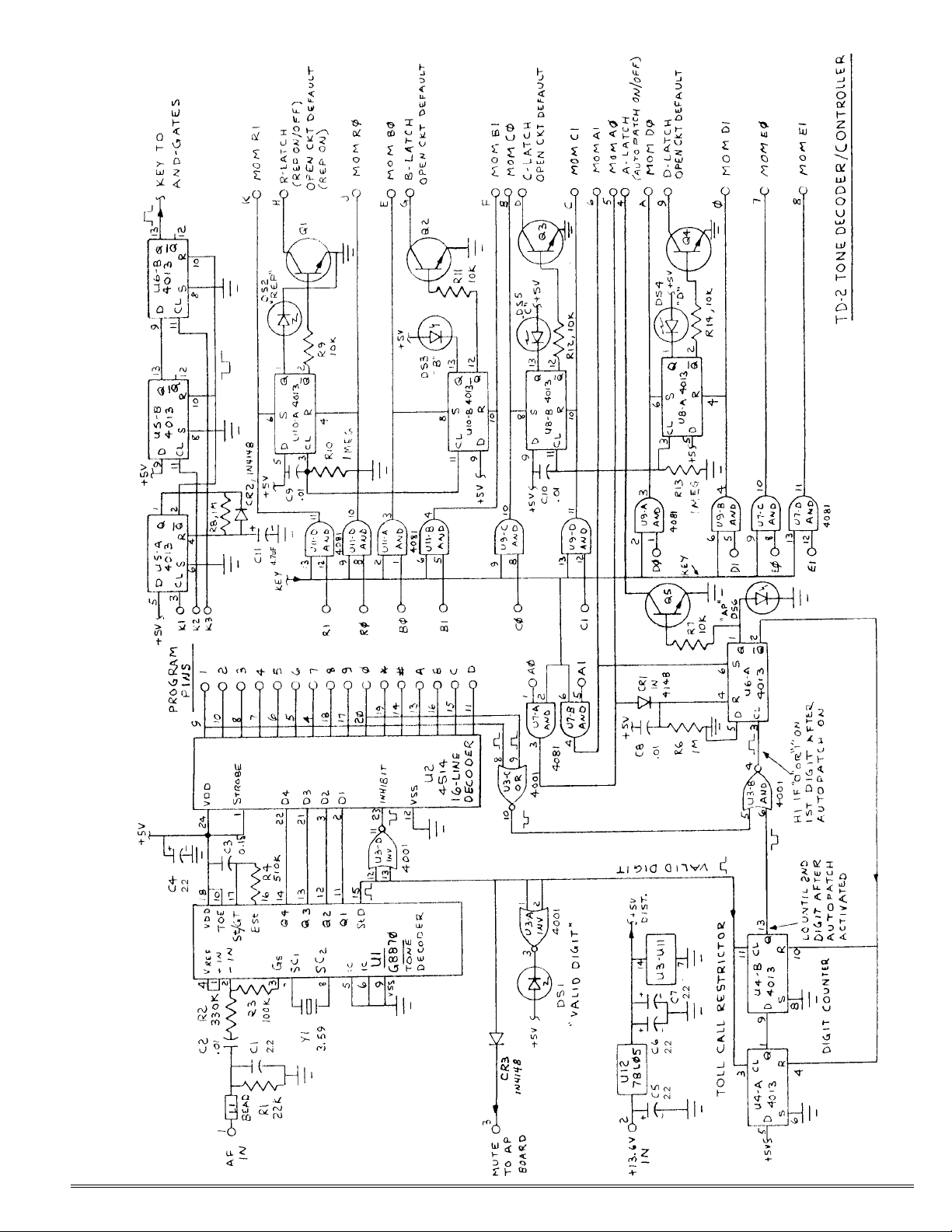
Refer to schematic diagram. The
input to tone decoder chip U1 is processed through a dial tone filter and a
bandsplit filter using switched capacitor technology. The signal is then
analyzed by two zero-crossing detectors and a digital detection algorithm
to determine if and which tones are
present. Then, the resulting logic signals are processed in a code converter
and latch circuit to provide four binary outputs (called Q1-Q4) with encoded information about dtmf digits
which may have been received.
A valid digit strobe (StD) signal indicates when any valid digit tones are
received. This valid digit signal is
used to gate U2 and to provide a muting signal to the autopatch board
when tones are received. It also operates the toll call restrictor, which is
discussed later. The whole circuit is
run on a clock controlled by color
burst crystal Y1. The audio input
signal is filtered by L1/C1 to remove
any rf which may be picked up on the
wiring. The ratio of R2-R3 sets the
gain of the op-amp input circuit. C3R4 sets the length of time necessary
for presence of valid tones and the interval between tones to prevent erratic
operation. U2 decodes the hexadecimal information from U1 to provide 16
CMOS output lines corresponding to
the digits on a DTMF pad. Programming for the various functions is done
by soldering jumper wires from program pads at the output of U2 to ad-
jacent function program pads.
The 4013 latches may be operated
synchronously or directly. The Q output will assume a hi whenever the set
input is triggered by a hi or a lo whenever the reset input is triggered by a
hi. The not-Q output is just the inverse. The latch also may be operated
synchronously, with its Q output assuming the whatever state the data
input has applied when the clock input receives a hi. If the clock input is
lo, the latch ignores the data input.
But if the clock goes hi at any time,
the latch will follow the data input
when the clock is hi.
U5A/B and U6B are D-type flipflops operating as a "key" latch in conjunction with program inputs K1-K3.
The output of U6B is high only upon
proper receipt of a three digit code,
which provides a security "key" to
unlock the rest of the logic gates.
R8/C11/CR2 in the reset circuit of
U5A provides a five-second time delay.
When the first digit of the key is received, the not-Q output of U5A releases the reset inputs of the other
two flip-flops for about five seconds. If
the full three digit code is not completed within that time period, all
three flip-flops are reset.
There are 12 momentary functions,
each using a 4081 ANDgate. Normally, one input of each AND-gate is
tied to the so-called "key" bus coming
from U6B and the other input is tied
to a programming pad bearing the
name of the output line from the ANDgate. To actuate a function, it is necessary to send the three-digit key plus
a fourth digit indicating the desired
function. During the interval when
the key is active (about five seconds),
if any other function is selected, it
may be activated with just its one digit
function code. If the key period expires, then the key must be re-sent to
start another command. It is also
possible to eliminate the key altogether, if the security is not needed,
allowing one digit commands at any
time. This is done by disconnecting
the input of the AND-gate normally
connected to the key bus and reconnecting it to the +5V bus instead. You
can even use the key for some functions and not others; using only a "#",
for instance, to turn off the autopatch,
but requiring the full four digits to
turn it on.
When a particular AND-gate receives both a key input and a function
input, it applies a hi signal to its output line. In the case of five pairs of
AND-gates, the outputs also are tied
to the "set" and "reset" inputs of
latches. The latches, in turn, drive
output transistors and led's. The
open-collector transistor switches may
be used to drive external circuits.
Thus, the momentary outputs, which
are CMOS hi's in the active state, may
be used or the latch outputs may be
used or any combination of latch and
momentary outputs may be used as
desired.
The names of the lines were selected based on two parameters.
First, the letter indicates the function
usually associated with the line. The
"R" function normally is used to enable or disable a repeater. The "A"
function normally controls an autopatch in a repeater. Of course, the
circuits can be used for any other
function, but it was thought best to
select names based on uses most
owners will have for them. The other
functions are not dedicated to any
particular function; so they were
named B, C, D, and E. (E is the pair
of momentary functions which has no
latch. We loaded the pc board with all
the functions we could fit on the
board, and we had two AND-gates left
to provide the extra momentary functions. There is no other significance.
If you need a momentary function or
two, you can use the E functions
without feeling you are wasting an associated latch.) The number, 1 or 0,
indicates which line turns the latched
output on or off.
It is a little confusing looking at
the latch circuits until you realize that
the repeater latch circuit is different
from the others, which turn on a circuit by the collector of the transistor
conducting to ground. The R latch
mutes a repeater by grounding the
COS line from the receiver or autopatch to the COR board input. Thus,
the repeater is off when the transistor
is active instead of being on when the
transistor conducts like the other circuits. The autopatch latch is different, too, because of extra toll call
restriction circuits. There also is a
difference in the way that the latches
are preset at power up. The repeater
wants to be enabled after a power
failure, not disabled. So its latch is
wired to default with the repeater enabled. The other latches default in
the off condition. Default status is
set by the C/R networks on the clock
or reset inputs of the latches. When
power is first applied, a positive pulse
is applied by the capacitor to reset the
©1999 Hamtronics, Inc.; Hilton NY; USA. All rights reserved. Hamtronics is a registered trademark. Revised: 2/4/03 - Page 1 -
Page 2

latches.
The autopatch latch has some extra circuitry with it to provide toll call
restriction. U4 is a counter which
keeps track of which digit is received
after the autopatch latch is turned on.
When the autopatch is off, the not-Q
output of U6A is hi, keeping U4A/B
reset. However, when the four digit
code is sent to bring up the patch,
U6A turns on, and the reset signal is
removed from U4, allowing it to count
digits. The Q output of U4B remains
lo until the second digit after the
autopatch turns on. If a 0 or 1 is received during the first digit after the
patch is brought up, U3B, which is
used as an AND- gate, is satisfied that
it has two lo's, and it provides a clock
input to autopatch latch U6A. Since
the data input is wired lo, that causes
the output of the latch to assume the
data input (lo) condition, thereby killing the autopatch. If any other digit is
received as the first digit of a phone
number, U3B is not satisfied, and the
autopatch remains on. On subsequent
digits, digit counter U4 removes its lo
from U3B, so the patch will not be
turned off by any received digit, even a
0 or 1.
CONSTRUCTION.
The pc board is double-sided with
plated-through holes. Because it is
more difficult to unsolder from this
type of board, be sure parts are oriented properly and of the correct
value before soldering. Pc traces are
close together, so use a fine soldering
iron tip.
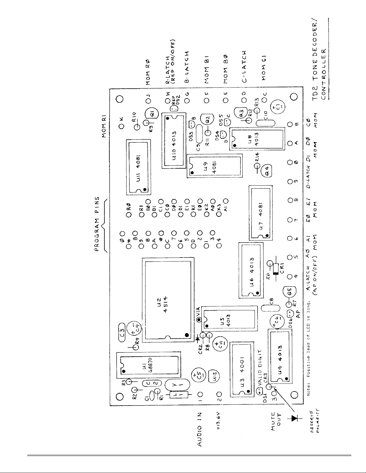
During construction, orient the
board right side up as shown in the
parts location diagram. The top side
as shown has the pin number markings. Also refer to the parts list and
schematic diagram during construction.
Before assembly, it is important to
decide whether or not you will use the
three digit key for controlling all of the
functions. If you will want to control
some or all of the functions with only
a single digit code, it is necessary to
break some pc paths on the top of the
board which will be concealed later by
ic sockets. If you want to modify the
pc board in this way, refer to the section on Programming prior to assembly.
CAUTION. The CMOS ic's used in
this kit are all static sensitive; so handle them with care. A grounded wrist
strap should be worn whenever you
pick up an ic. Do not open the packages containing the ic's until you are
ready to install them, and then handle
them only with suitable static control
measures.
a. Install ic sockets oriented with
notches as shown, and solder.
b. Install the led's on the board,
observing polarity. The positive lead
is longer on some led's. On others,
there is a flat on one side as shown on
the parts location diagram.
CAUTION: Small LED's are heat
sensitive. Keep the LED's up off the
board about 1/4 inch and solder
quickly, applying minimum heat to
avoid damage.
c. Install the remaining parts
other than the dip ic's, according to
the parts list. Be sure to observe polarity on the diodes, transistors, U12,
and the electrolytic capacitors. Vertically mounted parts are illustrated
with a circle indicating the body of the
part, and the diode symbol next to
CR2 on the diagram indicates the polarity.
d. Check over construction to be
sure all parts are installed in proper
places and with proper polarity and
that solder connections are good.
Look for things like cold solder joints
and solder splashes. Note that one
hole above U5 is a "via" used only to
make a connection between the top
and bottom of the board. Nothing is
installed in this hole. Note also that
programming wires will be installed
later.
e. Using static protection described earlier, carefully unpack the
dip ic's and install them in the sockets. Be sure to orient them as shown,
according to either dot or notch on the
end of each ic. If any conflict between
notches and dots on an ic, the notch
(which only appears on one end) takes
precedence. Sometimes, RCA cmos
ic's have a test dot of some color (eg.
blue) on one end, and such dots can
be confusing because they can appear
on either end. Ignore such dots if the
ic also has a notch or white bar on
one end, which would indicate the pin
1 end. Be careful to engage all the
pins in the socket; don't let any leads
bend over.
PC BOARD HANDLING PRECAUTION.
Be careful whenever you handle
the module. Even though static damage occurs most easily before ic's are
installed in their sockets, damage can
still occur to the ic's in a completed
module if a static discharge occurs at
any part of the board during handling.
Although wrist straps are not absolutely necessary just to handle the
completed board, you should make it
a habit of discharging your hand to a
grounded object before touching a
CMOS module.
INITIAL TESTING.
Although it is not necessary, you
may wish to test the tone decoder portion of the board before you proceed
with programming. To do so, connect
a power supply ground to the ground
trace at one of the four corners of the
board, and connect +10 to +15 Vdc to
the dc input at pad 2. Connect a
source of touch tones to audio input
pad 1, with a level between 100 mV
and 2V p-p. The outputs at the left
two rows of programming pads should
have a CMOS logic level (close to 0
and +5V) with the hi corresponding to
reception of a valid touch tone digit.
The "mute" signal should also appear
at mute pad 3 at the edge of the board
whenever any valid digit is received.
PROGRAMMING.
The following discussion is an attempt to simplify the steps required to
plan how to use the various functions
on the TD-2 module. There are many
variables involved, but breaking it
down like this should make it easier
to consider everything.
Read through the paragraphs
which follow, and take actions where
appropriate. Table 1 is a sample of the
type of plan you should make. This is
a typical setup in an amateur radio
repeater installation, and it is the programming we use for wired units at
the factory unless something else is
requested. The chart shows the correspondence of the decoder output pads
with the function-input programming
pads for each function. It also shows
the complete command sequence desired for each function, based on having to send the three "key" digits plus
the function-indicator digit for each
command. You should make a plan
like this for your installation, noting
what each function will be used for.
There are 12 momentary functions
available. 10 of them may be used either for a simple momentary function
or as the input to control a latching
function. The E0 and E1 functions
may be used only as momentary functions. (Refer to theory of operation for
more information on these circuits.)
The five latching functions are
similar except that the R function, being normally used for control of a repeater, has reversed nomenclature,
ie., the "R0" function causes a short to
ground at the latch transistor output
pin, and the "R1" function causes an
open circuit. The other latching func-
©1999 Hamtronics, Inc.; Hilton NY; USA. All rights reserved. Hamtronics is a registered trademark. Revised: 2/4/03 - Page 2 -
Page 3

tions are just the opposite. (See Theory of Operation for reason why.) The
A latch normally is used for autopatch
operation. It has toll call restriction
circuitry connected to it. If used for
some other function, the toll call restrictor can be eliminated by simply
breaking the pc traces to pins 8 and 9
of U3, and reconnecting those inputs
to ground instead.
Any of the functions not required
to turn a latch on and off may be used
for some momentary purpose. Because the E functions are momentary
only, they should be considered first
for momentary applications.
The latching outputs can be used
to drive solid state circuits directly
and can drive small relays to switch
power loads. The output transistors
can sink loads up to +15V and 50 mA.
If you drive an inductive load, like a
relay coil, be sure to connect a diode
with reverse polarity across the load
to absorb any inductive spikes which
could damage the transistor.
The momentary outputs are essentially the outputs of CMOS gates.
They provide about +5V in the active
state and close to ground in the passive state. Output current is no more
than 3 mA.
When you select programming
codes, you can use any touch tone
digit for any function you want. You
can reuse digits as many times as you
want; there is no need to use each
digit only once. The fan-out capabilities of U2 allow it to drive any number
of AND-gate inputs from any digit
output pad. The mechanics of making
connections are more of a limitation.
The board uses wire jumpers for programming. This allows easy field programming without prom burners, etc.,
but it does require a little planning
and workmanship. If you analyze the
sample programming in Table 1, you
will see that it provides for maximum
use of all the digits with nearby function pads to make wiring neat. Any
codes can be programmed, though,
and if neatness and ease of programming are not important to you, then
you have more freedom in selecting
codes.
Programming is done by soldering
2-1/2 inch lengths of hookup wire
stripped about 1/4 inch on each end.
That length allows a little slack so
wires can be moved around to allow
access to solder other wires.
Be sure to terminate the inputs to
all the AND-gates by connecting any
unused function programming pads
(not the digit output pads, but the
AND-gate input pads) to ground. If
the gate inputs are left floating, the
operation of the ic's can be erratic and
can affect other functions that are
used. Noise input can also cause
unterminated ic's to draw more current.
Normally, the three digit "key" is
used as the first part of any command, and the fourth digit indicates
the function. However, if the security
is not needed and you don't mind having someone accidently perform a control function by hitting one digit, the
pc board can be modified to provide
single-digit operation of one or more
functions. An example of this is that
some repeater owners want to be able
to turn off the autopatch with a single
digit, such as "#", even though the full
four digits are required to turn it on.
Also, in an industrial control operation, you might want to have quick
commands to perform repeated operations without having to dial up a "key"
sequence each time. Bear in mind
that the "key" provides useful functions; so consider what you are giving
up before you make a decision to opt
for a single digit command.
Unfortunately, the only way the pc
board could be laid out was to put the
"key" bus trace on the top of the
board. This means, you may need to
modify the traces under the ic sockets
for U7, U9, or U11 to change to single
digit operation, depending on whether
you only want to change an individual
function, a group of functions, or all
the functions to single-digit operation.
If you compare the schematic diagram
with the pc board, you will note the
"key" bus pc trace running on the top
of the board from U6 at its lower-left
extreme to U11 at its upper-right extreme and making a right-angle turn
just below the lower-right programming pad.
The AND-gate pad(s) you wish to
reprogram for single digit operation
must be disconnected from the "key"
bus by cutting the pc trace, and such
pad(s) must be reconnected by a bus
wire jumper to +5V instead, which you can
access on pin 14 of each
4081 ic. The jumpers, of
course, can be soldered
under the board, but
you must have access to
break the "key" bus on
the top of the board. If
you have a unit which is
already wired, you may
need to carefully unsolder the ic socket for necessary access. If you are
reprogramming more
that one function, you
may be able to break
ProgramPads Function _ Full Sequence
*---K1 "Key" 1st digit
1---K2 "Key" 2nd digit
2---K3 "Key" 3rd digit
0---R0 Repeater Off * 1 2 0
9---R1 Repeater On * 1 2 9
#---A0 Autopatch Off * 1 2 #
3---A1 Autopatch On * 1 2 3
8---B0 Aux B Off * 1 2 8
7---B1 Aux B On * 1 2 7
5---C0 Aux C Off * 1 2 5
6---C1 Aux C On * 1 2 6
B---D0 Aux D Off * 1 2 B
A---D1 Aux D On * 1 2 A
D---E0 Aux E0 Momentary Only * 1 2 D
C---E1 Aux E1 Momentary Only * 1 2 C
Table 1. Typical Programming Plan.
and reconnect a whole section of the
"key" bus instead of individual ic pins.
You may reduce the number of digits in the "key" by reconnecting U5
and U6 latch inputs. For a 2-digit key,
disconnect 3rd digit key latch, U6B,
"D" input from U5B and connect U6
pin 9 to +5V instead. Then, use the
K1 and K3 programming pads as your
"key" inputs. U5B essentially is out of
the circuit.
If you want a 1-digit "key", then
disconnect the "key" bus line from
U6B pin 13 and connect it to U5A pin
1 instead. Use K1 as your "key" input
for programming.
Here is a trick suggested by a customer on how to convert to a one-digit
key after the board has been assembled using the 4 digit method. Remove U6, bend pin 13 out, and reinstall U6 making sure pin 13 does
not connect with pin 13 on the IC
socket. Now jumper pin 13 and pin
14 of U6 by soldering the pins together on the bottom of the board.
TESTING PROGRAMMED
BOARD.
After the board has been programmed, all of the functions may be
tested. Power up the board as done
for Initial Testing on page 2; apply
touch tones of proper level; and check
for proper responses at the momentary and latching outputs with a voltmeter. You can also monitor the "key"
bus line on the board with a voltmeter
to see that it goes hi for about five
seconds after the 3-digit key is sent
and then returns to lo. The "mute"
output can be checked at pad 3 at the
left side of the board to see that it
goes hi whenever any valid digit is received.
You can also check the toll call restrictor circuit by attempting to dial
various numbers after the autopatch
latch is turned on. If you dial a 0 or 1
as the first digit after the patch is
brought up, the patch latch should
©1999 Hamtronics, Inc.; Hilton NY; USA. All rights reserved. Hamtronics is a registered trademark. Revised: 2/4/03 - Page 3 -
Page 4
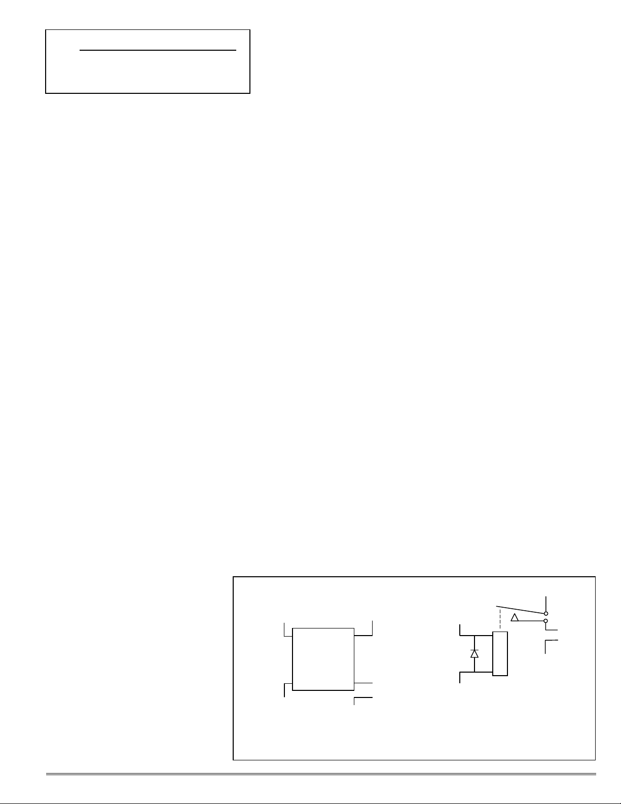
Table 2. DTMF Frequencies
A
A
1209 Hz 1336 Hz 1477 Hz 1633 Hz
697 Hz 1 2 3 A
770 Hz 4 5 6 B
852 Hz 7 8 9 C
941 Hz * 0 # D
dump. It should not dump if any
other digit is sent first or if a 0 or 1 is
sent after the first digit in the phone
number.
INSTALLATION.
Caution. Be careful whenever you
handle the module. Even though static
damage occurs most easily before ic's
are installed in their sockets, damage
can still occur to the ic's in a completed
module if a static discharge occurs at
any part of the board during handling.
Although wrist straps are not absolutely necessary just to handle the
completed board, you should make it a
habit of discharging your hand to a
grounded object before touching a
CMOS module.
Mounting.
The board should be mounted to
your chassis with 4-40 standoffs
about 3/8 inch long in the four corners of the board. Be sure to get a
good dc and signal ground through
the mounting hardware. If you cannot get ground through the hardware
or if you need a ground lug to solder
to, you can mount a solder lug under
the mounting screw in one corner of
the board. Placement of the board is
not critical, but the board should not
be mounted in a strong rf field. In a
repeater, the transmitter already is
shielded; so usually, you don't need to
do anything special. In our REP-100
Repeater, the TD-2 normally is
mounted under the left side of the
chassis, toward the front.
Power.
The unit is designed to operate on
+10 to +15Vdc at about 15 mA. The
low power consumption is due to the
CMOS circuitry. A voltage regulator
on the board takes care of voltage
variations within the range specified,
but be sure you use filtered dc power
and don't allow any spikes or reverse
polarity to be applied.
Tone Inputs.
The range of audio tone levels
which the tone decoder ic will accept
is 100 mV to 2V peak-peak. Audio
can be applied from any source, including radio receivers, and telephone
lines with some sort of interface such
as an autopatch board. The audio
source must be referenced to ground.
Check to be sure that your
source is compatible. If not,
some adjustment will have to be
made. If you cannot alter the
level from your source to within
this range, you may be able to
change the sensitivity of the
tone decoder to some extent.
The input circuit of U1 is a typical opamp, with gain set by the ratio of
R3/R2. A reasonable change in resistor values can be made to reset the
range of levels the chip will accept.
If you interface with our AP-1
Autopatch Board, you don't need to be
concerned about compatibility. The
tones for the TD-2 should come from
E8 on the Autopatch Board.
Output Circuits.
The latch outputs are opencollector transistor circuits, which can
be used to sink current up to 50 mA
on circuits up to +15V. The Theory of
Operation and Programming sections
tell more about the default condition
and control line terminology. If you
use the outputs to operate small relays, be sure to put a reverse diode
across the relay coil to soak up transients.
The "R" latch output should be
used if you want to enable and disable
a repeater by remote control. The "R"
output is normally used in our REP100 Repeater to ground the COS line
coming from the receiver or autopatch
to the COR board. This prevents the
transmitter from being keyed after the
"R0" command is given.
The "A" latch output should be
used to turn an autopatch on and off.
In our REP-100 Repeater, the "A" output grounds E13 of the AP-1 Autopatch Board to turn on the autopatch.
The "Mute" output from pad 3
normally is connected to E10 on our
AP-1 Autopatch Board to mute the
transmitter audio whenever a valid
digit is received so that it cannot be
heard on the air.
+
+
Output of
TD-2 Xstr
Figur e 3 A. So lid S tate R e lay
Wiring.
C Hot
To AC Load
AC
Common
Momentary outputs are direct
CMOS outputs from 4081 and-gates.
They provide close to +5V in the active
state and close to ground in the passive state. CMOS outputs will provide
only low current levels, up to about 3
mA.
Switching Large Loads.
In applications where the TD-2 is
used to turn equipment on and off,
the output transistor in the TD-2 can
be used to turn a relay on and off.
Two types of relays can be used.
Figure 3a shows a solid state relay,
such as the A95 relay we sell as an
accessory. The positive input of the
relay goes to +12Vdc and the negative
input goes to the TD-2 output. Note
that solid state relays generate heat;
so the metal base of the relay must be
coated with heatsink compound and
mounted to a metal box or other metal
object to dissipate the heat. The A95
relay is rated to switch ac current up
to 10A, at voltages of 24 to 220Vac.
The other type of setup is to use a
small relay, drawing less than 50mA,
to switch ac to operate a large power
contactor, as shown in figure 3b, or
used to switch a small load directly.
In this case, make sure you have a diode connected as shown to prevent
damage from transients generated
when the relay coil is turned off.
LED Indicators.
There are led's on the board to indicate the status of the various functions: one for each latch and one to
indicate when a valid digit is received.
Although these were included primarily for use in testing, it is possible to
remove them from the board and carefully extend them to a front panel with
hookup wire.
OPERATION.
Operation is fairly simple. A control sequence normally consists of
four digits, with the first three being a
C Hot
+
Common
Output of
TD-2 Xstr
Fig ure 3B . Small R e la y
Switching Power Contactor.
To
Contactor
Coil
AC
©1999 Hamtronics, Inc.; Hilton NY; USA. All rights reserved. Hamtronics is a registered trademark. Revised: 2/4/03 - Page 4 -
Page 5
common "key" used with all com-
y
mands, and the fourth digit being a
function identifier. As soon as the
fourth digit is received, the selected
function is performed.
If some or all of the functions have
been modified for operation with a
smaller "key" or no "key" at all, then
operation will be different for those
functions. For security, the entire
command sequence must be sent
within about five seconds or a timer
will reset and the sequence must be
started from scratch.
Note that the "key" timer will keep
the key circuit enabled for about five
seconds once it is tripped. Therefore,
if more than one command is to be
sent in a short period of time, only the
final digit of the second and following
commands need be sent. If you resend the "key" digits during the five
second period, they will be taken as
function identifier digits and not "key"
digits and may cause erroneous operation.
For example, using the commands
in our example, Table 1, if we want to
turn the autopatch on and then off
again within the five seconds, we
would send "* 1 2 3" to turn it on and
just "#" to turn it off, since the "* 1 2"
is still "in memory", so to speak because the "key" timer is still on.
TROUBLESHOOTING.
Tracking down trouble is fairly
straightforward. The Theory of Opera-
tion section describes the signal path
and what each circuit does. The only
significant voltages are CMOS hi's
(near +5V) and lo's (near ground) as
marked on the schematic by thelittle
pulse symbols. The only exception is
the latch output transistors, which
have about +0.7V at the base when
turned on. The collector is at ground
when conducting and open circuited
when off.
The operating voltage of the unit is
+10 to +15Vdc. Current drain normally is about 15mA, depending on
how many led's are lit, since they
draw more current than the other circuits.
Note that led brightness may vary
from one led to the next. To save
power and space on the board, the
led's are driven directly by the CMOS
ic's. In this mode, the ic's put out just
as much current as they can into
what looks like almost a short circuit
load. The amount of short-circuit
current varies from one chip to the
next, and so the brightness of the
led's vary. This should cause no concern, since the function of the led is
simply to indicate whether the circuit
is on or off.
A logical troubleshooting procedure would be to start by checking the
audio source to be sure valid tones of
proper level are being fed into the TD-
2. The range of acceptable levels is
100 mV to 2V peak-peak. Table 2
gives frequencies of touch tones. You
should check your tone pad if some of
the digits don't respond, to see if the
pad is sending tones on frequency. If
the U1 chip is not decoding touch
tones, check to see if its oscillator is
running and at the proper frequency.
You may need to use a 10:1 scope
probe for the frequency counter input
to keep from loading the oscillator circuit. The next step would be to check
the hexidecimal signals from U1 to U2
and check for a valid digit signal from
pin 15 of U1 (the valid digit led should
light).
Remember that the ic's are static
sensitive. You don't want to further
damage the board while troubleshooting. A ground wrist strap should be
worn when handling the ic's.
The next thing to check is the "key"
bus. Check to see if the output of
U6B at pin 13 goes hi when the "key"
digits are received. Next, check the
momentary outputs: R0, R1, A0, A1,
etc. Finally, check the 4013 latches to
see if they are responding and supplying the required current to turn on the
output transistors. The led's can be
used as an indicator of latch status.
If falsing occurs with some commands or the unit fails to respond,
you should check the twist of the incoming tones in addition to their frequencies. Twist is the relationship
between the level of tones in the high
group to the level of tones in the low
group. There should be no more than
10 dB difference between the two tone
levels in any digit. That is about a 3:1
difference in voltage. Various factors
influence the twist of the tones, in-
Suggested Selective Calling Unit Circuitr
cluding the tone pad at the transmitter, coupling capacitor values in your
system, receiver de-emphasis, transmitter pre-emphasis, and how hard
you drive the tones at the transmitter.
One problem with some transmitter
setups is that a ham will set his tone
level too high, trying to get full 5 kHz
deviation. The level is actually set so
high as to go into limiting. This may
cause the high and low tones to be
transmitted at the same level instead
of having the desired pre-emphasis. It
may also add distortion to the tones.
Then the receiver de-emphasis at the
other end causes the low tone to be at
a higher level than the high tone because the pre-emphasis at the transmitter was wrong. You should
encourage system users to be conservative in setting tone levels at their
transmitters.
Another cause of bad twist on
touch tones can inadvertently occur if
a sub-audible tone decoder is used in
the receiving system. The high-pass
filters supplied on sub-audible tone
decoder boards, usually connected in
series with the audio in the receiver to
get rid of buzz from sub-audible tones,
can severely degrade the levels of
lower frequency touch tones as well.
If you have such a board installed in
your receiver audio path, you might
want to check its effect on touch tone
twist. If a problem, you may want to
take your touch tones from a point in
the receiver unaffected by the highpass filter or even just not use the filter in your6 receiver. Generally, the
required level of deviation to make a
sub-audible tone system work is very
low, about 0.2 KHz or less, and some
people run the level much higher than
needed, which causes the buzz. Running the proper level may allow the filter to be removed with no great
problem.
©1999 Hamtronics, Inc.; Hilton NY; USA. All rights reserved. Hamtronics is a registered trademark. Revised: 2/4/03 - Page 5 -
Page 6

CUSTOMIZING.
There are several parameters
which are preset to what is considered
normal, but you may wish to change
them if settings don't do what you
want.
The first is the duration of tone
presence necessary to be recognized
as a valid digit. This is set, along with
minimum time required between digits, by R4/C3. The present setting is
what is considered normal in the telephone industry, namely 40-50 mSec.
You may wish to change it so you can
dial faster (but with possible falsing)
or slower (for more protection).
Another parameter you can play
with is the five second timer setting
for the window after reception of the
"key" digits during which other tones
will be accepted as function indicators. This is set by the R8/C11 time
constant. You could shorten the time
experimentally to find a time which
requires someone to really send the
four digits quickly and allow no additional time to do other commands. Or
you could slow it down so that it
would allow a series of commands to
be sent with one digit each after the
initial "key" digits are sent.
The gain of the input op-amp in U1
can be changed within reason to allow
various ranges of audio levels to be
accepted. The gain is set by the ratio
of R3/R2.
SOME ADDITIONAL TRICKS
YOU MAY BE INTERESTED
IN FOR USE WITH THE TD-2.
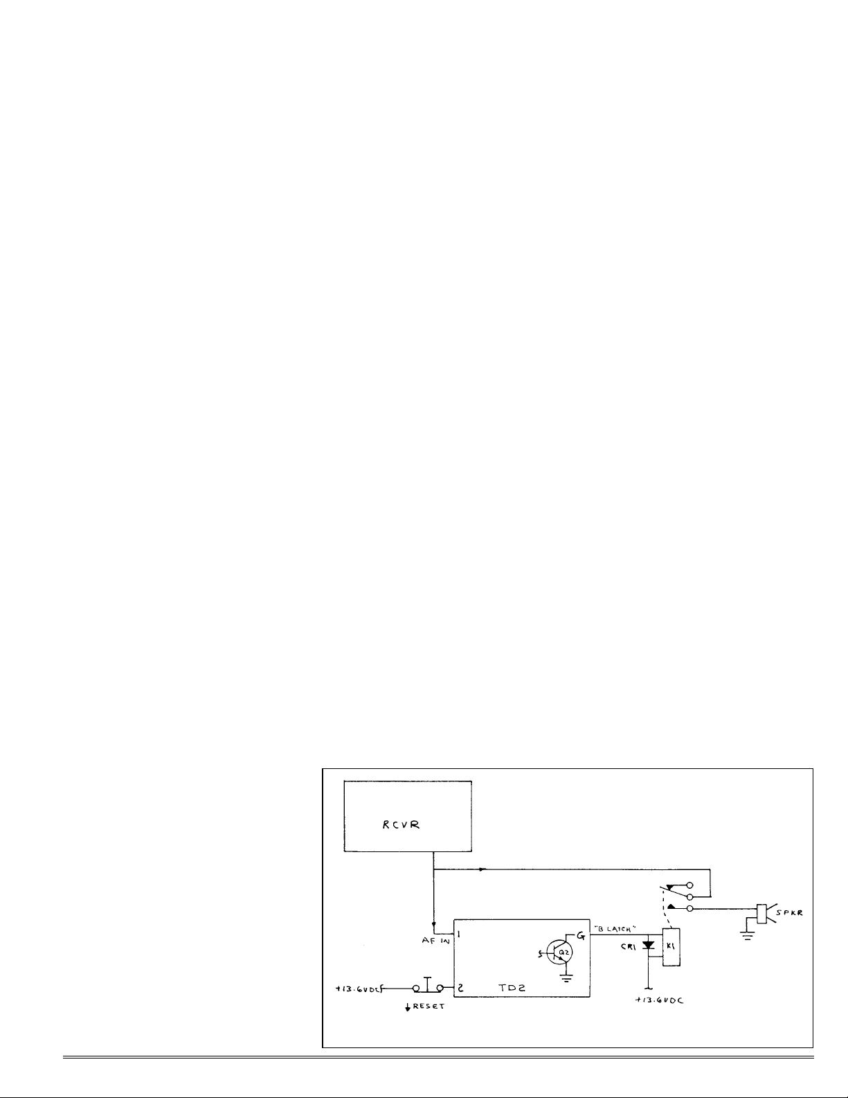
SELECTIVE CALLING UNIT.
The following diagram illustrates
how you can use a TD-2 module as a
selective calling unit with the addition
of only a few parts. This allows you to
monitor an fm radio channel for calls
directed only to you and mute the
speaker the rest of the time.
The receiver audio is routed to the
TD-2 input and also via relay K1 contacts, which mute the relay unless the
"B latch" function is activated at the
TD-2. The TD-2 requires an audio input level of 100 mV to 2 V p-p for
proper operation. If you run the re-
ceiver audio at a low to moderate level
(less than 1/10th watt), you can connect the TD-2 input at pad 1 directly
to the speaker output of the receiver.
If you plan to crank the speaker level
up fairly high, you may exceed the allowable level into the TD-2 and cause
blocking of tones. In such a case, either build a simple L-attenuator with
about 1000 ohms in series and 100
ohms in shunt from pad 1 to ground
or connect the TD-2 to the discriminator in the receiver after the deemphasis network.
Since the default condition of the
"B latch" in the TD-2 at power up is
"off", the speaker relay will operate
only after the required tone sequence
is received for the "B" function. The
speaker may be turned off again either
by momentarily breaking the B+ to the
TD-2, as shown in the diagram with
the push-button normally-closed
switch, or by sending the proper tone
sequence to turn off the "B latch" in
the TD-2, which of course can be done
by the sending station remotely.
The output transistor in the latch
circuit can switch up to 50 mA. Any
small relay with a coil resistance over
250 ohms can be used. Reed relays
are ideal. Although 13.6 Vdc is shown
in the diagram for relay power, any
voltage up to 15 Vdc can be used if
compatible with your relay. Be sure
to connect a reverse diode across the
relay coil to protect the transistor
from inductive spikes. If you like, an
LED can be connected across the relay coil too and located on your front
panel to indicate when the audio circuit is open.
DEFEATING THE TOLL CALL RESTRICTOR.
If you plan not to use the toll call
restrictor, the easiest thing to do is
break the traces from the "0" and "1"
lines to pins 8 and 9 of U3-C. Since it
is never good practice to leave a
CMOS gate input floating, pins 8 and
9 should be connected to ground.
If you want to be able to turn the
toll call restrictor on and off with one
of the latching functions of the TD-2,
break the ground trace between pins 7
and 8 of U4 and connect a 1K resistor
from pin 8 to the +5 V bus at U4 pin
5. You can turn the toll call restrictor
on by grounding pin 8 of U4 with any
of the extra latch outputs you may
have available. U4 pin 8, the "set" input of second stage of the digit counter in the toll call restrict circuit, will
block operation of the toll call restrictor when pin 8 is ungrounded because the resistor applies a hi unless
the controlling latch grounds pin 8.
With the "set" input constantly high,
the counter output remains high and
U3-B thinks you have already passed
the first digit in the phone number.
PARTS LIST.
Ref # Value (marking)
C1 .001 uf (102, 1nM, or 1nK)
C2 .01 uf disc (103)
C3 0.15 uf mylar (red)
C4-C7 2.2 uF electrolytic
C8-C10 .01 uf disc (103)
C11 4.7 uF electrolytic
CR1-CR3 1N4148 diode
DS1-DS6 Miniature red led
L1 Ferrite bead
Q1-Q5 2N3904 or 2N4124
R1 22K
R2 330K
R3 100K
R4 510K
R5 Not used
R6 1 meg
R7 10K
R8 1 meg
R9 10K
R10 1 meg
R11-R12 10K
R13 1 meg
R14 10K
U1 GTE/Mitel G8870 Tone
Decoder
U2 4514B Hex - 16 Line
Decoder
U3 4001B Quad Nor Gate
U4-U6 4013B Dual D Flip-Flop
U7 4081B Quad And Gate
U8 4013B Dual D Flip-Flop
U9 4081B Quad And Gate
U10 4013B Dual D Flip-Flop
U11 4081B Quad And Gate
U12 78L05 Regulator
Y1 3.59 MHz Color Burst
Crystal
©1999 Hamtronics, Inc.; Hilton NY; USA. All rights reserved. Hamtronics is a registered trademark. Revised: 2/4/03 - Page 6 -
Page 7
©1999 Hamtronics, Inc.; Hilton NY; USA. All rights reserved. Hamtronics is a registered trademark. Revised: 2/4/03 - Page 7 -
Page 8
©1999 Hamtronics, Inc.; Hilton NY; USA. All rights reserved. Hamtronics is a registered trademark. Revised: 2/4/03 - Page 8 -
 Loading...