

Page 1

Table of contents
Service Manual
Circuit Diagrams
Adjustment Procedure
HM303-5
Y-Preamplifier CH I (YP-Board) .................................. 4
Y-Preamplifier CH II (YP-Board) ................................. 5
Y-Intermediate Amplifier and Trigger Amplifier
(YP-Board) ................................................................. 6
YPA-Board (Bottom side) .......................................... 7
YPA-Board (Top side)................................................. 8
XY-Board (X-Amplifier) ............................................... 9
XY-Board (Y-Amplifier) ............................................. 10
XY-Board (Top side) ................................................. 11
Sync.-Amplifier ........................................................ 12
Timebase ................................................................. 13
Sweep-Generator .................................................... 14
TB-Board ................................................................. 15
CRT-Board ............................................................... 16
CRT-Board (Top and Bottom side) ........................... 17
Power Supply (PS-Board) ........................................ 18
PS-Board (Bottom side) .......................................... 19
PS-Board (Top side) ................................................. 20
Component tester, Calibrator .................................. 21
CCT-Board (Top and Bottom side) ........................... 22
Front-Controlboard .................................................. 23
Front-Controlboard (Top and Bottom side) .............. 24
Adjustment procedure .......................................... 25
Interface commands ............................................. 43
St. 010998. Hüb/goRR
Subject to change without notice
1
Page 2

2
Subject to change without notice
Page 3
Technische Daten
Vertikal-Ablenkung
Betriebsarten: Kanal I oder II einzeln,
Kanal I und Kanal II alternierend oder chop.,
(Chopperfrequenz ca. 0,5MHz)
Summe oder Differenz von KI und KII,
(beide Kanäle invertierbar),
XY-Betrieb: über Kanal I und Kanal II
Frequenzbereich: 2xDC bis 35MHz (−3dB)
Anstiegszeit: <10ns
Überschwingen: ≤ 1%
Ablenkkoeffizienten: 12 kalibrierte Stellungen
von 5mV/cm bis 20V/cm (1-2-5 Teilung)
variabel 2,5:1 bis mindestens 50V/cm
Genauigkeit der kalibrierten Stellungen: ±3%
Y-Dehnung x5 (kalibriert) bis 1mV/cm ±5%
im Frequenzbereich 0 - 10MHz (–3dB)
Eingangsimpedanz: 1MΩ II 20pF
Eingangskopplung: DC-AC-GD (Ground)
Eingangsspannung: max. 400V (DC + Spitze AC)
Triggerung
Automatik (Spitzenwert):
Normal mit Level-Einstellung: DC-
LED-Anzeige für Triggereinsatz
Flankenrichtung: positiv oder negativ,
Alternierende Triggerung von KI und KII,
Quellen: Kanal I, Kanal II, Netz, extern
Kopplung: AC (10Hz bis 100MHz),
Extern: ≥0,3V
Aktiver TV-Sync-Separator (pos. und neg.)
DC (0 bis 100MHz),
LF (0 bis 1,5kHz)
ss
<20Hz-100MHz
>
100MHz (≤5mm)
von 30Hz bis 30MHz
(≤5mm)
Horizontal-Ablenkung
Zeitkoeffizienten: 20 kalibrierte Stellungen
von 0,2s/cm - 0,1µs/cm mit 1-2-5 Teilung
Genauigkeit der kalibrierten Stellungen: ±3%
variabel 2.5:1 bis max. 0,5s/cm
mit X-Mag. x10 ±5%; 10ns/cm: ±8%
Holdoff: variabel bis ca. 10:1
Bandbreite X-Verstärker: 0-3MHz (−3dB)
Eingang X-Verstärker über Kanal II,
Empfindlichkeiten wie Kanal II
X-Y Phasendifferenz: <3° unter 220kHz
Komponententester
Testspannung: ca. 6V
Teststrom: ca. 5mA
Testfrequenz: ca. 50Hz
Testkabelanschluß: 2 Steckbuchsen 4mm ∅
Prüfkreis liegt einpolig an Masse (Schutzleiter)
(Leerlauf)
eff
(Kurzschluß)
eff
Verschiedenes
Röhre: D14-364GY/123 oder ER151-GH/-,
Rechteckform (8x10cm), Innenraster
Beschleunigungsspannung: ca. 2000V
Strahldrehung: auf Frontseite einstellbar
Kalibrator: Rechteckgenerator (t
≈1kHz / 1MHz; Ausgang: 0,2V ±1% und 2V
Netzanschluß: 100-240V ~±10%, 50/60Hz
Leistungsaufnahme: ca. 36 Watt bei 50Hz
Zul. Umgebungstemperatur: 0°C...+40°C
Schutzart: Schutzklasse I (IEC1010-1/VDE 0411)
Gewicht: ca. 5,6kg, Farbe: techno-braun
Gehäuse: B 285, H 125, T 380 mm
Mit verstellbarem Aufstell-Tragegriff
<4ns)
a
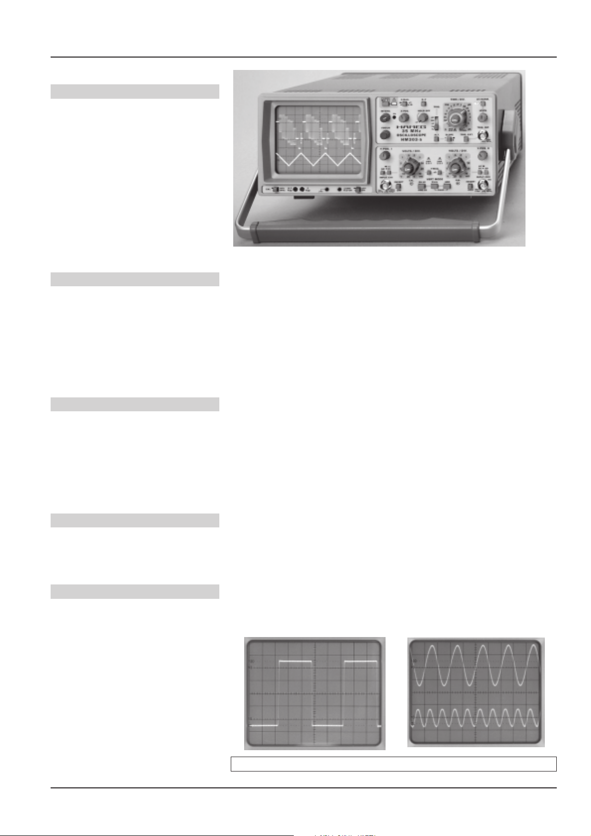
35MHz Standard Oszilloskop HM 303
,
Vertikal: 2 Kanäle, 5mV – 50V/cm, mit Dehnung x5 ab 1mV/cm
Zeitbasis: 0.5s – 0,1µs/cm, mit Dehnung x10 bis 10ns/cm
Triggerung: DC – 100MHz, TV-Sync-Separator, Altern. Triggerung
Komponenten-Tester, 1kHz/1MHz Kalibrator
Der neue HM303 ist der Nachfolger des bisher weltweit mehr als 180000mal
verkauften HM203. Wesentliche Neuerungen betreffen vor allem die Erhöhung
der Bandbreite von 20 auf 35MHz, die Erweiterung des horizontalen Ablenkbereiches bis max. 10ns/cm und eine nochmalige Verbesserung der schon seit
Jahren einzigartigen Triggerung. In seiner jetzigen Ausführung eignet sich der
HM303 f ür die Darstellung von Signalen im Frequenzbereich von DC bis ca. 100
MHz.
Ein wesentliches Qualitätsmerkmal dieses Oszilloskops ist vor allem die
hohe Übertragungsgüte der Meßverstärker mit max. 1% Überschwingen.
Damit diese – von der Tastspitze bis zum Bildschirm – ständig kontrollierbar ist,
besitzt der HM303 als erster seiner Preisklasse einen Kalibrator mit geringer
Anstiegszeit.
Wirklich außergewöhnlich ist die Triggerung des HM303. Bereits ab 5mm
Bildhöhe kann sie noch Signale bis über 100MHz triggern. Für die exakte
Darstellung von TV-Signalen wird ein aktiver Sync-Separator verwendet. In
alternierender Betriebsart ist auch die Triggerung von zwei Signalen mit
unterschiedlicher Frequenz möglich. Wie sein Vorgänger ist das Gerät ebenfalls
mit dem bewährten Komponententester ausgestattet. Seine Meßspannung ist
jetzt amplitudenstabilisiert. Vorbildlich ist auch die Stromversorgung. Das eingebaute Schaltnetzteil arbeitet ohne Netzspannungsumschaltung immer mit dem
geringstmöglichen Leistungsverbrauch. Gegen magnetische Einwirkungen von
außen ist die Strahlröhre des HM303 mit Mumetall abgeschirmt.
Alles in allem hat HAMEG mit diesem Gerät wieder einmal Maßstäbe
gesetzt, die entsprechend seinem Preis-/Leistungs-Standard einfach beispiellos
sind. Kenner werden von den Eigenschaften des neuen HM303 begeistert sein.
Foto: 1MHz Rechteck-Signal
Foto: 50MHz und 100MHz Sinus-Signal
mit alternierender Triggerung
Subject to change without notice
01/98
Inkl. Zubehör: Netzkabel, Betriebsanleitung, 2 Tastköpfe 1:1/10:1
3
Page 4
Y-Preamplifier CH I (YP-Board)
4
Subject to change without notice
Page 5
Y-Preamplifier CH II (YP-Board)
Subject to change without notice
5
Page 6
Y-Intermediate Amplifier and Trigger Amplifier (YP-Board)
6
Subject to change without notice
Page 7
YPA-Board (Bottom side)
Subject to change without notice
7
Page 8
YPA-Board (Top side)
8
Subject to change without notice
Page 9
XY- Amplifier
Subject to change without notice
9
Page 10
XY Board (Y Amplifier)
10
Subject to change without notice
Page 11
XY Board (Top and Bottom side)
Subject to change without notice
11
Page 12
Sync.- Amplifier
12
Subject to change without notice
Page 13
Timebase
Subject to change without notice
13
Page 14

Sweep- Generator
14
Subject to change without notice
Page 15

TB Board
Subject to change without notice
15
Page 16

CRT- Board
16
Subject to change without notice
Page 17

CRT Board (Top and Bottom side)
Subject to change without notice
17
Page 18

Power Supply (PS-Board)
+12V
9
MPT
B1011
2
1
5
MPT
C1036
10u 250V
L1007
68uH 1.5A
BYD37M
D1020
6
+
1K0
R1016
R1070
D1023
LL4151
T1004
R1066
+185V
6
MPT
L1006
BYD37M
D1021
100u 16V
C1032
C1045
1K00
R1063
TO-126
BD434
3
3
7K50
+141V
+
+
68uH 1.5A
7
0.1u 50V
2k21
2
c
T1012
BC850
C1030
10u 250V
+
+
C1028
22u 160V
D
R1072
3K32
IC1005
1
SOT-23
C1037
0.1u 250V
C1031
22u 160V
1K0
R1071
3
21
TO-92A
TL431C
619R
R1062
MKT
7
MPT
L1005
8
+12V
C1029
+13.5V
+
68uH 1.5A
C1026
+
D1004
BYV27-100
9
R1061
10K0
R1054
3K01
D1015
LL4151
R1053
619R
1000u 16V
330u 25V
8
IC1004A
TL082CN
R1055
1
T1008
c
T1010
BC850
SOT-23
3
+
1
511R
2
c
BC860
31
C1046
0.1u 50V
2
-
3
SOT-23
2
10
100u 16V
C1034
+
R1056
10K0
C1042
T1002
3
R1043
R1052
C1023
+
C1022
+
C
-12V
1n 50V
21
TO-126
BD433
7K50
R1014
511R
1000u 16V
L1004
330u 25V
10
MPT
12K1
R1051
0R39
8
MPT
-13.5V
68uH 1.5A
BYV27-100
D1003
13
MPT
P1002
12
MPT
HT1
D1009
BYD37M
MOLEX6S
1
2
HT1
BLV
3
+
R1022
+
4
G1
C1009
6
5
HT14
-1950V
100u 35V
1K82
R1073
100u 16V
C1015
BLV
31V
BYT01-400
D1012
21
16
MPT
C1038
R1025
11
MPT
2
R1074
27k4
1K0
HT14
31
75K
+
1u 50V
R207
WIRE6
P1003
P1010
WIRE6
6.3V
20
T1006
BF822
R1029
3
2
C1016
12345
1
2
BYD37M
D1014
19
FOKUS
1M00
B1001
1
T1005
R1006
470K
0.1u 100V
6
6
3
4
5
DD1400
D1016
B
C1007
R1024
LL4151
D1005
c
BC860
SOT-23
D1010
13
10n 400V
1M00
R1036
R1003
470K
R1004
BZV55C75
HVC
-2025V
1M00
R1028
750K
R1023
750K
C1010
0.1u 100V
470K
14
MPT
141516
17
R1042
-1950V
15
MPT
G1
C1019
10n 2kV
17
MPT
DD1400
D1024
750K
R1007
1M00
C1043
R1041
R1040
0R0
VR37
R1012
6M81
C1024
68p 3KV
10n 50V
475K
10K0
R1027
R1044
3
1M00
750K
R1058
5
6
+
7
475K
2
BYD37M
D1027
DD1400
D1025
R1034
R1064
-
IC1004B
TL082CN
R1057
4K32
T1007
BF822
1
C1018
10n 400V
18
10M0
VR37
47K5
D1018
LL4151
R1067
1K00
R1046
22K1
SOT-23
BYD37M
D1026
R1011
C1004
47n 2kV
R1069
8K25
A
+12V
WIRE6
P1008
P1009
WIRE6
Title : Rev.:
6
+185V
6
R
5
+141V
5
2
3
4
2
3
4
Date :
Document Number :
1
+12V
-12V
1
12345678
BYD77G
D1022
D1017
220p 400V
C1027
D1019
BYD77G
BYD37M
5
DR1001
ETD39/303
4
B1010
R1018
R1065
1K3
1K3
R1068
100K
411
10n 400V
MKT
C1035
R1017
C1033
0.1u 400V
MKT
100K
411
R1047
R207
56K2
R1013
R1049
200K
R1037
332K
301K
R1050
1
+
C1025
68u 400V
+
3
2
D1001
R1048
68u 400V
C1011
FL406
F1001
0.5AF
L1003
220uH 1A
1
MPT
87654321
C1001
4700p
Y 250V
D
8K25
1
D1006
LL4151
5
1K00
R1019
LINE
4
0.1u
C1002
X2 250V
3
MPT
STHV82FI
T1003
1
2
22K1
B1007
IC1001
6
32
14
L1001
2x33mH 1A
C1021
100p 2kV
32
1
c
ISOWATT 218
T1009
BC860
SOT-23
3
2
3
T1011
BC850c
2
4
C1005
2200p
Y 250V
C
R1015
R1059
1K00
1
SOT-23
2
CNY17-2Z
R1021
R1031
200K
0.33u
C1003
X2 250V
2W
0R22
C1044
C1039
4n7 50V
T1001
BUX86
3
75K
R1001
U
R1005
R1060
4K99
1n 50V
TO-126
1
R1020
NTC 8
S14K275
1
2
MPT
R1030
75K
D1013
LL4151
R1035
22R
12.9V
681R
VR37
R1002
3
332K
2
3
6
R1010
90R9
R207
C1006
R1009
R1045
10K0
851
IC1003
2200p
Y 250V
90R9
R207
D1011
BAS20
1K0
R1008
R1033
R1026
R1032
R1038
D1007
BZV55B16
B
23
1K82
47K5
5K11
0R0
S1001
2
3
IC1002
21
4
0.4V
4
7
NT
C1012
+
C1017
1u 50V
TO-92A
TL431C
MPT
R1039
+
1n 250V
200R
C1040
0.1u 50V
C1041
0.1u 50V
C1020
220u 16V
P1001
Power Recept.
P1005
+13.5V
B1013
A
WIRE6
6
B1003
LINE
8
5
+Vcc
3
4
IC1004C
-12V
+12V
1
2
B1009
B1008
-12V
+12V
4
-Vcc
TL082CN
-13.5V
18
Subject to change without notice
Page 19

PS-Board (Top side)
Subject to change without notice
19
Page 20

PS Board (Bottom side)
20
Subject to change without notice
Page 21

Component tester, Calibrator
Subject to change without notice
21
Page 22

CCT Board (Top and Bottom side)
22
Subject to change without notice
Page 23

Front- control board
Subject to change without notice
23
Page 24

Front Control board (Top and Bottomside)
24
Subject to change without notice
Page 25

Adjustment
Procedure
Subject to change without notice
25
Page 26

ADJUSTMENT PROCEDURE
30MHz Standard Oscilloscope HM303-5
WARNING
The Instrument must be disconnected from the mains power supply whenever you open
the case, repair or exchange parts.
HIGH VOLTAGE WARNING!
Hazardous High Voltage of up to 2,000 Volts is present inside this Instrument. The areas particularly
affected by High Voltage are the high voltage circuit on the PS-board, the CRT-board and the CRTsocket.
SERVICE AND ADJUSTMENT
• of this instrument should only be performed in accordance and in conjunction with the operating
manual and the WARNINGS contained therein.
• should only be performed by suitable qualified and experienced service personnel, or should be
referred to one of the HAMEG companies listed on the rear cover of the manual.
Test Instruments required:
1) Scope Tester HZ60-2.
2) Constant amplitude sinewave generator, 20Hz - 250MHz, output 5mV - 5V into 50Ω,
preferably with 20dB attenuation (e.g. HM8133, TEK SG502 + TEK SG503).
3) Amplitude Calibrator with 1kHz squarewave output and 600Ω impedance, risetime faster than
150ns.Output voltage 2mV - 20Volts in 1-2-5 sequence for 4 divisions display amplitude
(e.g. HZ62, TEK PG506).
4) Time mark generator from 5ns/div to 5s/div. Output min. 10mV into 50Ω
(e.g. HZ62, TEK TG501).
5) Pre-attenuator 2:1 (1MΩ , 12-48pF), e.g. HZ20.
6) 50Ω BNC through termination, e.g. HZ22.
7) 2 BNC-cables, 50Ω, e.g. HZ34.
8) BNC-T-connector.
9) Oscilloscope probe 10:1, with exactly 9MΩ series resistance and compensated
for test oscilloscope mentioned under 10).
10) Oscilloscope 100MHz, 5mV/div to 5V/div, e.g. HM1005.
11) Trimming/adjusting tool.
12) Variable output safety insulation transformer.
13) Video signal generator with positive and negative signal output.
14) Yt-EPROM HM1007.
26
This procedure covers all adjustments and the most important - but not all - performance checks.
The correct sequence of all adjustment steps must be strictly followed.
Exact adjustment is only possible when any influence of the earths‘ magnetic field has been
compensated with the trimmer marked TR (trace rotation).
All adjustments should only be performed by qualified and experienced personnel. This is particularly
important for adjustments in the high voltage section of the instrument.
Subject to change without notice
Page 27

Table of Contents
(1) R1008: +141 Volt supply............................................................................. 29
(2) R1016: +12 Volt supply............................................................................... 29
(3) VR7000: Trace Rotation Check. .................................................................. 29
(4) R1004 : CRT minimum intensity................................................................. 29
(5) R712RT maximum intensity........................................................................ 29
(6) R712: Mean Y-plate Potential Channel I. .................................................... 29
(7) R714: Mean Y-plate Potential Channel II. ................................................... 29
(8) RV6021 : Astigmatism correction. .............................................................. 31
(9) R640: Y-Gain CH I. ...................................................................................... 31
(10) R122: FET operating point CH I. ................................................................. 31
(11) R203: Invert-Balance CH I. ......................................................................... 31
(12) R177: Variable-Balance CH I. ...................................................................... 31
(13) R139: 100Hz Squarewave 5mV/div CH I. ................................................... 32
(14) R134: 100Hz Squarewave 1mV/div Adjustment CH I. ............................... 33
(15) R658: Y-Gain CH II. ..................................................................................... 33
(16) R422: FET operating point CH II. ................................................................ 33
(17) R503: Invert-Balance CH II. ........................................................................ 33
(18) R477: Variable-Balance CH II. ..................................................................... 33
(19) R439: 100Hz Squarewave 5mV/div CH II. .................................................. 33
(20) R434: 100Hz Squarewave 1mV/div CH II. .................................................. 33
(21) RV2005 (A), RV2006 (C), CV2000 (D) and CV2001 (B): Y-Final Amplifier. .. 35
(22) Y-Amplifier Bandwidth Check. .................................................................... 35
(23) C113/111/102/105: Attenuator Compensation CH I. .................................. 35
(24) C413/411/402/405: Attenuator Compensation CH II. ................................. 35
(25) R663: ADDition/Offset................................................................................ 37
(26) RV2417 (A), RV2418 (B): Overscan. ........................................................... 37
(27) RV3519: Sweep start voltage. .................................................................... 37
(28) RV2225: X-Magnification x1. ...................................................................... 37
(29) RV2260: X-Symmetry. ................................................................................ 37
(30) RV3591 (A)/3589 (C), CV3511 (B): Time base. ........................................... 37
(31) RV2234: X-Magnification x10. .................................................................... 39
(32) R624: XY-Gain ............................................................................................. 39
(33) RV3293: Trigger-Symmetry......................................................................... 39
(34) R612: DC-Triggering CH I. .......................................................................... 39
(35) R603: DC-Triggering CH II. ......................................................................... 39
(36) RV2301 (A), 4322 (B): Component Tester Y-Position and Tilt. .................... 41
(37) VR8940: Calibrator Output. ........................................................................ 41
(38) Trigger Filter Check. .................................................................................... 41
(39) Triggerbandwidth Check. ............................................................................ 41
(40) External Trigger Check................................................................................ 41
(41) Video Trigger Check. ................................................................................... 42
NOTE
The adjustment procedures assume that the instrument had once been properly adjusted in the
factory and adjustments are required due to temperature drift or the replacement of defective
components.
Before starting each adjustment procedure, set the oscilloscope to the following basic settings:
• Press POWER pushbutton (in!).
• Release all other pushbuttons (out!) except AC/DC input coupling.
• Rotate the three variable controls (TIME/DIV. and VOLTS/DIV.) to
• Set TIME/DIV. switch to 50µs/div.
• Set both VOLTS/DIV switches to 5mV/div.
• Rotate the HOLD OFF knob fully counterclockwise.
• Trigger coupling set to AC.
• Set all other controls to their midrange positions.
If different settings are required, they are mentioned particularly for each subject.
Subject to change without notice
their (calibrated) detent positions.
27
Page 28

PS-Board
3
Front panel
1
7
2
YPA-Board
6
PS-Board XY-Board
28
5
4
Pin 2 Pin 4
Subject to change without notice
Page 29

(1) R1008: +141 Volt supply.
WARNING: To avoid damage use a fully insulated screwdriver!
Locate and identify R1008 (1) on PS-Board (screened section).
Locate 8 pole checkpoint socket on XY-Board and identify pin 2.
Adjust R1008 (1) for exactly +141Volts (± 0.1 Volt).
(2) R1016: +12 Volt supply.
Locate and identify R1016 (2) on PS-Board.
Locate 8 pole checkpoint socket on XY-Board and identify pin 4.
Adjust R1016 (2) for exactly +12Volts (± 10mV). All other voltages +185V (pin 1), -12V (pin 5)
and -1950V on cathode of CRT depend on the correct +12 Volt adjustment. All these
voltages must be checked and verified.
(3) VR7000: Trace Rotation Check.
Locate and identify VR703 (3) „TR“ on the front panel.
Using Y-Pos.I and X-Pos. controls, move baseline to the center of the graticule.
Press channel I GD pushbutton (in!).
When turning VR703 (3), check that the range of inclination of the baseline is at least 1mm at both
horizontal limits of the graticule.
Readjust baseline exactly parallel to the horizontal center line of the graticule.
(4) R1004 : CRT minimum intensity.
Locate and identify R1004 (4) on PS-Board.
Set INTENS. control to fully left position.
Press XY pushbutton (in!).
Adjust R1004 (4) so that the dot just disappears.
Release XY pushbutton.
(5) R1003 : CRT maximum intensity.
Locate and identify R1003 (5) on PS-Board.
Set INTENS. control to fully right position.
Set FOCUS knob on the front panel for optimum sharpness.
Adjust R1004 (5) so that the beam diameter is 1.5mm.
Repeat adjustment 4 and 5 until optimum is obtained!
(6) R712: Mean Y-plate Potential Channel I.
Locate and identify R712 (6) on YPA-Board.
Press DUAL pushbutton (in!).
Set both beams to the horizontal center line of the graticule by using Y-position I and II knobs
on the front panel. The Y-position knob settings must not be changed during the following
procedure until item 7) is finished.
Release DUAL pushbutton (out!).
Switch the oscilloscope OFF.
Locate and identify both lines from the Y-final amplifier to the Y-plates of the CRT.
Connect both lines (short)galvanically.
Switch the oscilloscope ON.
Measure the DC voltage at the Y-plates in respect to ground.
Adjust R712 (6) for +85Volt Y-plate voltage.
Note: Do not remove the short at the Y-plates until item 7) is finished.
(7) R714: Mean Y-plate Potential Channel II.
Note: Do not start item 7) until item 6) is finished.
Locate and identify R714 (7) on YPA-Board.
Press CHI/II pushbutton (in!) for channel II mode.
Measure the DC voltage at the Y-plates in respect to ground.
Adjust R714 (7) for +85Volt Y-plate voltage.
Switch the oscilloscope OFF.
Remove the connection between both Y-plates.
Switch the oscilloscope ON.
Subject to change without notice
29
Page 30

7
12
11 9
YPA-Board
30
10
PS-Board
8
Subject to change without notice
Page 31

(8) RV6021 : Astigmatism correction.
Locate and identify RV6021 (8) on CRT-Board.
Connect a 1MHz squarewave signal with 25mVpp at 50Ω (HZ22) to input CHI.
Set time base to 0.1µs/div.
Adjust FOCUS control for optimum sharpness.
Adjust RV6021 (8) until leading edge and top of signal have equal sharpness.
Recheck range of FOCUS control.
Adjust FOCUS control for optimum sharpness.
(9) R640: Y-Gain CH I.
Locate and identify R640 (9) on YPA-Board.
Connect a 25mV/1kHz squarewave signal via 50Ω cable and 50Ω through terminator
to input channel I.
Set time base to 1ms/div.
Adjust R640 (9) for 5 division signal height.
(10) R122: FET operating point CH I.
Locate and identify R122 (10) in CH I section of the YPA-Board.
Release all pushbuttons (out!) for channel I mode.
Press Y x5 channel I (in!) for 1mV/div.
Press GD pushbutton channel I (in!).
Switch the attenuator channel I constantly between 5mV/div (1mV) and 10mV/div (2mV).
Adjust R122 (10) until no Y-position change occurs.
Do not change the operating conditions.
(11) R203: Invert-Balance CH I.
Press GD pushbutton channel I (in!).
Press Y x5 channel I (in!) for 1mV/div.
Using Y-POS.I control set trace to the horizontal center line.
Locate and identify R203 (11) on YPA-Board.
Adjust R203 (11) so that the baseline will not move, when pressing and releasing the
INVERT CH I pushbutton.
(12) R177: Variable-Balance CH I.
Locate and identify VR177 (12) in CH I section of the YPA-Board.
Press channel I Y-MAG. x5 pushbutton for 1mV/div.
Press channel I GD pushbutton (in!).
Adjust VR177 (12) so that the baseline will not move when turning the channel I Y-variable
control through the entire range.
Check adjustment 11) again and repeat it if required.
Subject to change without notice
31
Page 32

181715
YPA-Board
20
19
16 13
(13) R139: 100Hz Squarewave 5mV/div CH I.
Locate and identify R139 (13) in CH I section of the YPA-Board.
Connect a 25mV/100Hz squarewave signal via 50Ω cable and 50Ω through
terminator to input channel I.
Set time base to 2ms/div.
Check that DC input coupling is selected.
Adjust R139 (13) for flat top.
14
32
Subject to change without notice
Page 33

(14) R134: 100Hz Squarewave 1mV/div Adjustment CH I.
Locate and identify R134 (14) in CH I section of the YPA-Board.
Connect a 5mV/100Hz squarewave signal via 50Ω cable and 50Ω through
terminator to input channel I.
Press Yx5 channel I (in!) for 1mV/div.
Set time base to 2ms/div.
Check that DC input coupling is selected.
Adjust R134 (14) for flat top.
(15) R658: Y-Gain CH II.
Locate and identify R658 (15) on YPA-Board.
Connect a 25mV/1kHz squarewave signal via 50Ω cable and 50Ω through
terminator to input channel II.
Check that DC input coupling is selected.
Set time base to 1ms/div.
Adjust R658 (15) for 5 division signal height.
(16) R422: FET operating point CH II.
Locate and identify R422 (16) in CH II section of the YPA-Board.
Press CHI/II pushbutton (in!) for channel II mode.
Press Y x5 channel II (in!) for 1mV/div.
Press GD pushbutton channel II (in!).
Switch the attenuator channel II constantly between 5mV/div (1mV) and 10mV/div (2mV).
Adjust R422 (16) until no Y-position change occurs.
(17) R503: Invert-Balance CH II.
Press GD pushbutton channel II (in!).
Press Y x5 channel II (in!) for 1mV/div.
Using Y-POS.II control set trace to the horizontal center line.
Locate and identify R503 (17) on YPA-Board.
Adjust R503 (17) so that the baseline will not move, when pressing and releasing the
INVERT CH II pushbutton.
(18) R477: Variable-Balance CH II.
Locate and identify VR477 (18) in CH II section of the YPA-Board.
Press channel II Y-MAG. x5 pushbutton for 1mV/div.
Press channel II GD pushbutton (in!).
Adjust VR477 (18) so that the baseline will not move when turning the channel I Y-variable control
through the entire range.
Check adjustment 17) again and repeat it if required.
(19) R439: 100Hz Squarewave 5mV/div CH II.
Locate and identify R439 (19) in CH II section of the YPA-Board.
Connect a 25mV/100Hz squarewave signal via 50Ω cable and 50Ω through terminator
to input channel II.
Set time base to 2ms/div.
Check that DC input coupling is selected.
Adjust R439 (19) for flat top.
(20) R434: 100Hz Squarewave 1mV/div CH II.
Locate and identify R434 (20) in CH II section of the YPA-Board.
Connect a 5mV/100Hz squarewave signal via 50Ω cable and 50Ω through terminator
to input channel II.
Press Yx5 channel II (in!) for 1mV/div.
Set time base to 2ms/div.
Check that DC input coupling is selected.
Adjust R434 (20) for flat top.
Subject to change without notice
33
Page 34

XY-Board
ACD B
24
YPA-Board
BDCA
23
34
Subject to change without notice
Page 35

(21) RV2005 (A), RV2006 (C), CV2000 (D) and CV2001 (B):
Y-Final Amplifier.
Connect a 1MHz squarewave signal of 25mV via 50Ω cable and 50Ω through termination
to input CH I.
Check that DC input coupling is selected.
Set time base to 0.2µs/div.
Locate and identify the adjustment points RV2005 (21A), RV2006 (21B), CV2000 (21C) and
CV2001 (21D) on XY-Board.
As the capacitive influence of the cabinet is of importance, a metal sheet above the Y-final
amplifier section is required.
Adjust RV2005 (21A) and CV2001 (21B) for flat top, RV2006 (21C) and CV2000 (21D) for fast
leading edge with minimum overshoot.
Repeat until optimum is obtained.
Check channel II under the same conditions.
(22) Y-Amplifier Bandwidth Check.
Connect a 40mVpp/50kHz sinewave signal from a constant amplitude generator via
a 50Ω throughtermination to the input of channel I.
Adjust the generator amplitude for 8 div. display height on the screen.
Increase the generator frequency until the signal is displayed with 5.6 div. height ( -3dB).
Repeat the adjustment under item 21), if the frequency reading on the generator shows a value
less than 30MHz.
Press CHI/II-TRIGI/II pushbutton (in!).
Connect a 40mVpp/50kHz sinewave signal from a constant amplitude generator via
a 50Ω throughtermination to the input of channel II.
Adjust the generator amplitude for 8 div. signal height displayed on the screen.
Increase the generator frequency until the signal is displayed with 5.6 div. height ( -3dB).
Repeat the adjustments under item 21), if the frequency reading on the generator shows
a value less than 30MHz.
(23) C113/111/102/105: Attenuator Compensation CH I.
Locate and identify trimmers VC102-113 for CH I on YPA-Board.
Check that DC input coupling is selected.
Check that input attenuator CH I is in 5mV/div setting.
Set time base switch to 0.5ms/div.
Set amplitude calibrator to 1kHz and connect a 2:1 pre-attenuator via 50Ω cable to input of CH I.
Set calibrator output voltage to 80mVpp (40mVpp at the 2:1 pre-attenuator output,
if terminated with 1MΩ).
Adjust trimmer in pre-attenuator for flat squarewave top. This adjustment must not be changed
during the following procedure.
Adjust compensation as listed in the table below:
Scope Input Adjustment
Input Atten. CH I
250mVpp 50mV/div A (VC111) flat top + B (VC113) leading edge
2.5Vpp 0.5V/div C (VC102) flat top + D (VC105) leading edge
(24) C413/411/402/405: Attenuator Compensation CH II.
Locate and identify trimmers VC402-413 for CH II on YPA-Board.
Check that DC input coupling is selected.
Check that input attenuator CH II is in 5mV/div setting.
Set time base switch to 0.5ms/div.
Set amplitude calibrator to 1kHz and connect a 2:1 pre-attenuator via 50Ω cable to input of CH II.
Set calibrator output voltage to 80mVpp (40mVpp at the 2:1 pre-attenuator output,
if terminated with 1MΩ).
Adjust trimmer in pre-attenuator for flat squarewave top. This adjustment must not be
changed during the following procedure.
Adjust compensation as listed in the table below:
Scope Input Adjustment
Input Atten. CH II
250mVpp 50mV/div A (VC411) flat top + B (VC413) leading edge
2.5Vpp 0.5V/div C (VC402) flat top + D (VC405) leading edge
Subject to change without notice
35
Page 36

YPA-Board
25
XY-Board
TB-Board
36
27
B30A
Subject to change without notice
C
Page 37

(25) R663: ADDition/Offset.
Press DUAL pushbutton (in!).
Locate and identify R663 (25) on YPA-Board.
Set input coupling CH I and II to GD.
Move both baselines with Y-POS. I and II controls to the horizontal center line of the graticule.
Release DUAL pushbutton (out!).
Press ADD pushbutton (in!).
Adjust R663 (25) for the same signal position as before in DUAL mode.
(26) RV2417 (A), RV2418 (B): Overscan.
Locate and identify RV2417 (26A) and RV2418 (26B)on XY-Board.
Press channel I and channel II GD pushbuttons (in!).
Press DUAL pushbutton (in!).
Set baseline with Y-POS.I control to the top line of the graticule.
Set baseline with Y-POS.II control to the bottom line of the graticule.
Adjust RV2417 (26A) for just lighting up of the upper LED.
Adjust RV2418 (26B) for just lighting up of the lower LED.
Repeat both procedures until both adjustments are correct.
(27) RV3519: Sweep start voltage.
Locate and identify RV3519 (27) on TB-Board.
Set time base to .2ms/div.
Locate and identify pin 7 of test socket on XY-Board.
Use a control oscilloscope with a x10 (10:1) probe and measure under DC input coupling
conditions the sawtooth voltage at pin 7.
Adjust RV3519 (27) for 0 volts DC at the sawtooth start (end of the hold off time).
(28) RV2225: X-Magnification x1.
Locate and identify RV2225 (28) on XY-Board.
Set time base to .2ms/div.
Adjust RV2225 (28) for 10.2 div sweep length.
(29) RV2260: X-Symmetry.
Locate and identify RV2260 (29) on XY-Board.
Set the X-POS. knob to the mechanical center position.
Adjust RV2260 (29) for a symmetrical trace position in respect to the graticule.
(30) RV3591 (A)/3589 (C), CV3511 (B): Time base.
a) Locate and identify RV3591 (A) on TB-Board.
Set time mark generator to f= 20kHz and connect signal to CH I input.
Set time base to 50µs/div.
Move trace with X-Pos. control so that the first time mark coincides with the first left
graticule line of the screen.
Adjust RV3591 (30A) so that the 11th time mark coincides with the last right graticule line.
Rotate time base variable control to fully left position.
Now more than 2.5 time marks per division should be displayed.
b) Locate and identify CV3511 (30B) on TB-Board.
Set time base to 0.5µs/div. and time base variable control to CAL position.
Set time mark generator to f= 2MHz.
Move trace with X-POS. control so that the first time mark coincides with the first left
graticule line of the screen.
Adjust CV3511 (30B) so that the 11th time mark coincides with the last right graticule line.
c) Locate and identify RV3589 (30C) on TB-Board.
Set time base to 5ms/div. and time base variable control to CAL position.
Set time mark generator to f= 200Hz.
Move trace with X-POS. control so that the first time mark coincides with the first left
graticule line of the screen.
Adjust RV3589 (30C) so that the 11th time mark coincides with the last right graticule line.
Check all time base settings with suitable time mark signals.
Subject to change without notice
37
Page 38

YPA-Board
35 32 34
TB-Board
XY-Board
33
38
Subject to change without notice
Page 39

(31) RV2234: X-Magnification x10.
Locate and identify RV2234 (31) on XY-Board.
Press pushbutton X-Mag. x10.
Set time base to 50µs/div.
Set time mark generator to f= 20kHz and connect signal to CH I input.
Set X-POS control to mechanical center.
Using X-POS control, move the visible time mark to the first left graticule line.
Adjust RV2234 (31) so that the next time mark coincides with the last (right) graticule line.
Release X-MAG. x10 pushbutton (out!).
(32) R624: XY-Gain
Connect a 1kHz squarewave signal of 25mVpp amplitude (HZ60-2) to input CH II.
Check that the CH II input sensitivity is 5mV/div.
Check that DC input coupling is selected.
Locate and identify R624 (32) on YPA-Board.
Press XY pushbutton.
Set X-POS control that the left dot coincides with the graticule center.
Adjust R624 (32) for a distance of 5 division between left and right dot.
(33) RV3293: Trigger-Symmetry
Locate and identify RV3293 (33) on TB-Board.
Connect a 50kHz sinewave signal of 40mVpp amplitude to input CH I.
Set input coupling CH I to AC.
Check that trigger coupling is in AC position.
Set attenuator switch CH I to 0.1V/div (calibrated position).
Press AT/NORM. pushbutton (in!).
Turn LEVEL control for triggering (center position).
Reduce signal height and correct LEVEL setting for just triggering with a minimum signal height.
Press and release the trigger SLOPE ± pushbutton and adjust RV3293 (33) for stable triggering
in both SLOPE conditions.
(34) R612: DC-Triggering CH I.
Locate and identify R612 (34) on YPA-Board.
Connect a 50kHz sinwave signal to input CH I.
Set generator amplitude to 8cm.
Set time base to 10µs/div.
Press AT/NORM. pushbutton (in!).
Turn LEVEL control to the center position.
Release AC/DC input coupling pushbutton CH I (out!).
Constantly switch between AC and DC trigger coupling and watch the trace start position.
Adjust R612 (34) so that there is no difference regarding the signal start position on the signal
slope between DC and AC trigger coupling.
(35) R603: DC-Triggering CH II.
Locate and identify R603 (35) on YPA-Board.
Connect a 50kHz sinwave signal to input CH II.
Press CH I/II-TRIG I/II pushbutton (in!).
Set generator amplitude to 8cm.
Set time base to 10µs/div.
Press AT/NORM. pushbutton (in!).
Turn LEVEL control to the center position.
Release AC/DC input coupling pushbutton CH II (out!).
Constantly switch between AC and DC trigger coupling and watch the trace start position.
Adjust R603 ( 35) so that there is no difference regarding the signal start position on the signal
slope between DC and AC trigger coupling.
Subject to change without notice
39
Page 40

XY-Board
Pin 1
CT-Board
37
Pin 14
36B
40
Subject to change without notice
Page 41

(36) RV2301 (A), 4322 (B): Component Tester Y-Position and Tilt.
Release all pushbuttons (out!).
Press COMPONENT TESTER pushbutton (in!).
Locate and identify RV2301 (36A) on XY-Board.
Adjust RV2301 (36A) to shift the approx. 8 div. horizontal component tester trace to the
horizontal center of the CRT graticule.
Locate and identify RV4322 (36B) on CC-Board.
Set up the instrument on a table in normal operating conditions to avoid misadjustment due
to the influence of the earth magnetic field.
Adjust RV4322 (36B) in such a way that the trace is parallel to the horizontal graticule center line
and not tilt. This adjustment
(37) VR8940: Calibrator Output.
Locate and identify VR8940 (37) on CC-Board.
Connect a digital multimeter to the 0.2Vpp calibrator output.
Set up the digital multimeter for DC measurement in a suited sensitivity setting.
Locate and identify IC8903 on CC-Board.
Connect pin 1 and pin 14 of IC8903 galvanically together.
Adjust VR8940 (37) for exactly 0.2V DC.
Check 2V calibrator output.
Remove the connection between pin 1 and pin 14 of IC8903.
Connect a 10:1 probe to the 0.2Vpp calibrator output and connect it to the CH I input of the scope.
Release all pushbuttons (out!).
Select CH I DC input coupling.
Set attenuator CH I to 5mV/div (calibrated detent).
Set time base to 0.2ms/div.
Now approximately 2 signal periods should be visible on the screen.
Press 1kHz/1MHz pushbutton (in!).
Set time base to 0.5µs position.
Check 1MHz calbrator signal.
Please note: Neither the calibrator frequency nor the pulse duty factor are specified.
(38) Trigger Filter Check.
Set time base to 1ms/div.
Connect a 1kHz sinewave signal of 40mVpp amplitude to input CH I and check for full
screen deflection.
Set input attenuator CH I to 50mV/div and check for 8mm display height.
Select trigger coupling from AC to DC and LF. The signal must always trigger .
Set sinewave generator to 50kHz and 40mV output amplitude and check for 8mm display height.
Select trigger coupling from AC to DC. The signal must always trigger.
Select LF trigger coupling. Now the signal should not trigger.
(39) Triggerbandwidth Check.
Set time base to 0.05µs/div, time base variable to CAL position.
Set input coupling switch CH I to DC.
Set trigger coupling to AC.
Release AUTO/NORM pushbutton (out!).
Set input attenuator CH I to 5mV/div.
Connect a 100MHz sinewave signal to input CH I.
Adjust generator output for 5mm display height.
The signal must be triggered.
(40) External Trigger Check.
Set time base to 20µs/div.
Set input attenuator CH I to 0.1V/div.
Connect a 50 kHz sinewave signal via a 50-Ohm through terminator with an amplitude of
280mVpp (100mVrms) to input CH I and check for 2.8div display height.
Set LEVEL to midrange position.
Check that the Trigger-LED is ON.
Press EXT. pushbutton. The Trigger-LED (TR) should now be OFF.
Subject to change without notice
41
Page 42

Set input coupling CH I to GD.
Remove signal cable from input CH I and connect it to TRIG.INP. socket. Do not change
generator settings.
Now the Trigger-LED should be ON again.
(41) Video Trigger Check.
Set CH I input coupling switch to DC.
Connect video signal with positiv sync. pulses to input CH I.
Adjust input attenuator switch CH I for 1 div display amplitude of video signal.
Set time base to 5ms/div ( time base ≥ 1ms/div = frame triggering).
Set trigger coupling switch to TV.
Check that trigger starts with vertical sync. pulses.
Now approx. 2.5 frames should be visible.
Change polarity of video signal.
Press SLOPE pushbutton (in!).
Again approx. 2.5 frames should be displayed triggered.
Set time base to 20µs/div ( time base range 0.5ms/div - 0.1µs/div = line triggering).
Recheck trigger SLOPE pushbutton procedure, using video signal with polarity change.
Note:Note:
Note: Invert pushbutton does not affect trigger polarity.
Note:Note:
42
Subject to change without notice
 Loading...