VISIBLE DETECTOR
γ
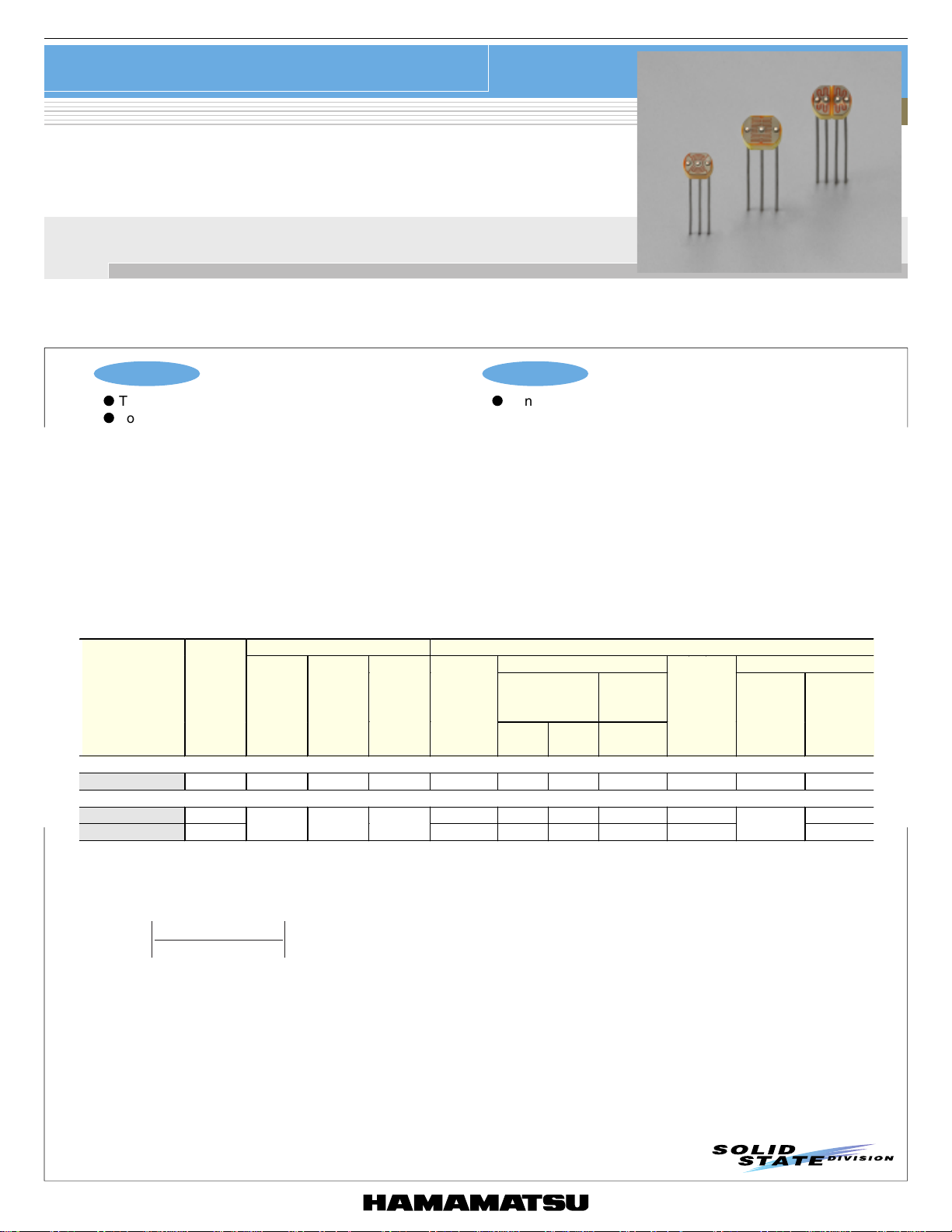
CdS photoconductive cell
Resin coating
·dual
type
Low cost dual-element sensor with standard size
CdS photoconductive cells utilize photoconductive effects in semiconductors that decrease their resistance when illuminated by light.
These sensors are non-polar resistive elements with spectral response characteristics close to the human eye (luminous efficiency), thus making
their operating circuits simple and small.
Dual-element sensors can be used to compare the signal from each element or perform signal processing by using a separation circuit.
Features
l
Thin substrate
l
Low price
Absolute maximum ratings / Characteristics (Typ. Ta=25 °C, unless otherwise noted, per 1 element)
■
Absolute maximum ratings Characteristics *
Supply
voltage
(Vdc) (mW) (°C) (nm)
➀
➁
➂
) - log (R10)
) - log (E10)
50 25
100 50
log (R
log (E
Dimensional
outline
100
100
Type No.
5R type
P1395-01
7R type
P2405
P2478-01
*1: All characteristics are measured after exposure to light (100 to 500 lx) for one to two hours.
*2: The light source is a standard tungsten lamp operated at a color temperature of 2856 K.
*3: Measured 10 seconds after shutting off the 10 lx light.
*4: Typical gamma characteristics (within ±0.10 variations) between 100 lx to 10
100
γ =
10
, E10: illuminance 100 lx, 10
E
100
, R10: resistance at 100 lx and 10
R
100
*5: The rise time is the time required for the sensor resistance to reach 63 % of the saturated conductance level (when fully
illuminated). The fall time is the time required for the sensor resistance to decay from the saturated conductance level to
37 %.
Power
dissipation
lx
P
respectively
lx
Ambient
temperature
Ta
-30 to +60
-30 to +60
sensitivity
wavelength
Applications
l
Sensor for various control device
1
Peak
p
λ
550 5 15 0.1 0.60 120 250
520 45 135 20 0.90 20
530 25 75 1 0.70
Resistance *
10 lx, 2856 K 0
Min.
(kΩ)
Max.
(kΩ)
2
10
3
*
lx
Min.
(MΩ)
lx
100 to 10
Response time 10
4
*
Rise timetrFall time
(ms) (ms)
lx
50
40
5
*
lx
tf

CdS photoconductive cell
Resin coating
·
dual type
■
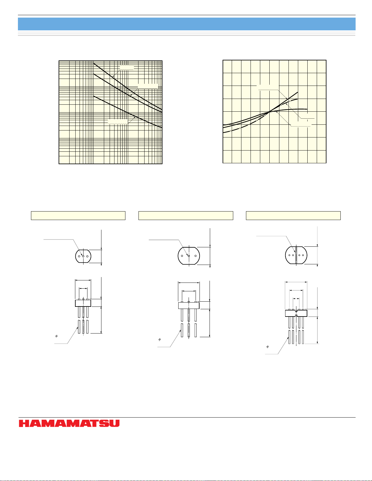
Resistance vs. illuminance
1000
100
10
(Typ. Ta=25 ˚C, light source: 2856 K)
RESISTANCE (kΩ)
1
P2405
P2478-01
P1395-01
■
Resistance vs. ambient temperature
140
120
100
80
(Typ. light source: 2856 K, 10 lx)
P2478-01
RELATIVE RESISTANCE (%)
0.1
0.1 1 10 100
ILLUMINANCE (lx)
■
Dimensional outlines (unit: mm)
KCDSB0020EA
60
-30 -20 0 20 40 60 80
AMBIENT TEMPERATURE (˚C)
➀ P1395-01 ➁ P2405 ➂ P2478-01
P2405
P1395-01
KCDSB0021EA
ACTIVE AREA
0.45
LEAD
5.1 ± 0.2
3.4
COMMON
4.3 ± 0.2
2.5 MAX.25 ± 2
KCDSA0004EA
ACTIVE AREA
0.5
LEAD
7.0 ± 0.2
5.0
COMMON
ACTIVE AREA
5.9 ± 0.2
7.0 ± 0.2
5.1
2.5 MAX.
27 ± 2
0.5
LEAD
KCDSA0005EA KCDSA0006EA
2.0
5.9 ± 0.2
2.5 MAX.
27 ± 2
Information furnished by HAMAMATSU is believed to be reliable. However, no responsibility is assumed for possible inaccuracies or omissions.
HAMAMATSU PHOTONICS K.K., Solid State Division
1126-1 Ichino-cho, Hamamatsu City, 435-8558 Japan, Telephone: (81) 053-434-3311, Fax: (81) 053-434-5184, http://www.hamamatsu.com
U.S.A.: Hamamatsu Corporation: 360 Foothill Road, P.O.Box 6910, Bridgewater, N.J. 08807-0910, U.S.A., Telephone: (1) 908-231-0960, Fax: (1) 908-231-1218
Germany: Hamamatsu Photonics Deutschland GmbH: Arzbergerstr. 10, D-82211 Herrsching am Ammersee, Germany, Telephone: (49) 08152-3750, Fax: (49) 08152-2658
France: Hamamatsu Photonics France S.A.R.L.: 8, Rue du Saule Trapu, Parc du Moulin de Massy, 91882 Massy Cedex, France, Telephone: 33-(1) 69 53 71 00, Fax: 33-(1) 69 53 71 10
United Kingdom: Hamamatsu Photonics UK Limited: 2 Howard Court, 10 Tewin Road, Welwyn Garden City, Hertfordshire AL7 1BW, United Kingdom, Telephone: (44) 1707-294888, Fax: (44) 1707-325777
North Europe: Hamamatsu Photonics Norden AB: Smidesvägen 12, SE-171 41 Solna, Sweden, Telephone: (46) 8-509-031-00, Fax: (46) 8-509-031-01
Italy: Hamamatsu Photonics Italia S.R.L.: Strada della Moia, 1/E, 20020 Arese, (Milano), Italy, Telephone: (39) 02-935-81-733, Fax: (39) 02-935-81-741
Specifications are subject to change without notice. No patent rights are granted to any of the circuits described herein. ©2001 Hamamatsu Photonics K.K.
Cat. No. KCDS1003E01
May. 2001 DN
 Loading...