VISIBLE DETECTOR
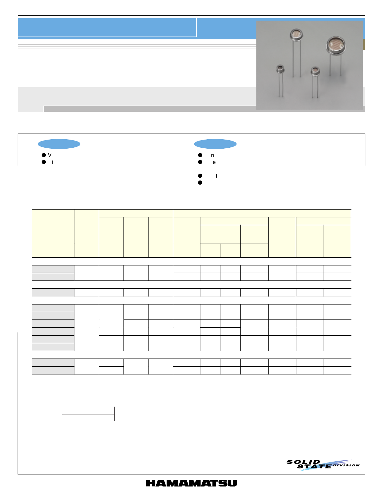
CdS photoconductive cell
Metal package type
Hermetically sealed for high reliability
CdS photoconductive cells utilize photoconductive effects in semiconductors that decrease their resistance when illuminated by light. These
sensors are non-polar resistive elements with spectral response characteristics close to the human eye (luminous efficiency), thus making their
operating circuits simple and small.
Features
l
Variety of package size
l
Highly resistant to moisture and dust
Absolute maximum ratings / Characteristics (Typ. Ta=25 °C, unless otherwise noted)
■
Absolute maximum ratings Characteristics *
, 10
Power
dissipation
100
300
lx
Supply
voltage
(Vdc) (mW) (°C) (nm)
➀
➁
➂
➃
) - log (R10)
) - log (E10)
100 30
150 50
200
100 100
400
lx
log (R
log (E
Dimensional
outline
100
100
Type No.
5M type (TO-18)
P1114-01 630 13 39 1 60 25
P1114-04
6M type (f5.5)
P930
8M type (TO-5)
P201B
P201D
P368 14 43
P380
P467
P534
12M type (TO-8)
P621 150 570 1.3 3.7 0.3 0.75 80 40
P3872
*1: All characteristics are measured after exposure to light (100 to 500lx) for one to two hours.
*2: The light source is a standard tungsten lamp operated at a color temperature of 2856 K.
*3: Measured 10 seconds after removal of light of 10
*4: Typical gamma characteristics (within±0.10 variations) between 100lx to 10lx
100
γ =
10
, E: illuminance 100
E
, R: resistance at 100lx and 10lx respectively
R
*5: The rise time is the time required for the sensor resistance to reach 63 % of the saturated conductance level (resistance
when fully illuminated). The fall time is the time required for the sensor resistance to decay from the saturated conductance
level to 37 %.
P
50
Ambient
temperature
Ta
-30 to +50
-30 to +70
-30 to +50
-30 to +60
-30 to +50
-30 to +60
-30 to +80
-30 to +60
lx
sensitivity
wavelength
.
Applications
l
Sensor for office machine
l
Safety device for heating system and boiler
(flame monitor for oil burner)
l
Night/day check sensor and sunlight sensor for air conditioner
l
Alarm and safety sensor
Peak
lp
570 15 45 10
560 7 23 0.5 0.68 60 90
5602163200.8525 20
5202060100.9030 10
620
520 8 24 5 0.90 50 20
560 1.3 3.7 0.05 0.55 70 100
540 5 15 1.0 0.80 40 30
Resistance *
10 lx, 2856 K 0 lx *
Min.
(kW)
Max.
(kW)
4.4 13
g
!
Min.
(MW)
100 to 10
0.80
20 0.85 35 20
Response time 10
"
*
Rise timetrFall time
(ms) (ms)
lx
40 20
lx
tf
#
*
1

3.5 ± 0.330 MIN.
PHOTOSENSITIVE
SURFACE
5.0
9.1 ± 0.3
8.1 ± 0.1
WINDOW 5.9 ± 0.2
0.4
LEAD
■
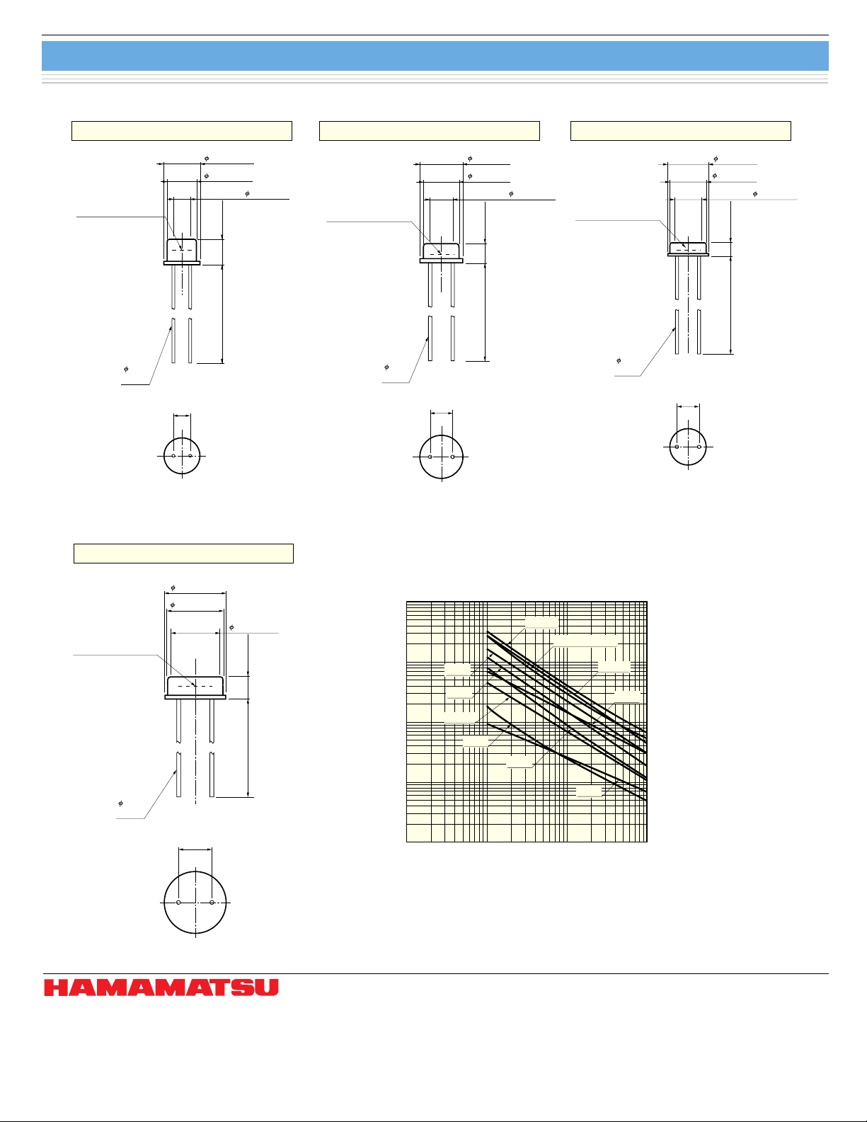
Dimensional outlines (unit: mm)
CdS photoconductive cell
Metal package type
➀ 5M type (TO-18)
PHOTOSENSITIVE
SURFACE
0.3
LEAD
2.5
5.35 ± 0.2
4.75 ± 0.1
WINDOW 3.0 ± 0.2
3.9 ± 0.2
30 MIN.
KCDSA0007EB
➁ 6M type
PHOTOSENSITIVE
SURFACE
0.3
LEAD
6.5 ± 0.3
5.5 ± 0.1
WINDOW 3.5 ± 0.2
3.4
3.6 ± 0.230 MIN.
KCDSA0008EA
➂ 8M type (TO-5)
KCDSA0009EB
➃ 12M type (TO-8)
PHOTOSENSITIVE
SURFACE
0.45
LEAD
13.9 ± 0.3
12.4 ± 0.2
7.5
WINDOW
10.9 ± 0.3
5.0 ± 0.3
30 MIN.
KCDSA0010EA
■
Resistance vs. illuminance
1000
100
(Typ. Ta=25 ˚C, light source: 2856 K)
P368
P467
10
P3872
P621
RESISTANCE (kΩ)
1
0.1
0.1 1 10 100
ILLUMINANCE (lx)
P201B
P1114-01/-04
P201D
P930
P380
P534
KCDSB0022EB
Information furnished by HAMAMATSU is believed to be reliable. However, no responsibility is assumed for possible inaccuracies or omissions.
HAMAMATSU PHOTONICS K.K., Solid State Division
1126-1 Ichino-cho, Hamamatsu City, 435-8558 Japan, Telephone: (81) 053-434-3311, Fax: (81) 053-434-5184, http://www.hamamatsu.com
U.S.A.: Hamamatsu Corporation: 360 Foothill Road, P.O.Box 6910, Bridgewater, N.J. 08807-0910, U.S.A., Telephone: (1) 908-231-0960, Fax: (1) 908-231-1218
Germany: Hamamatsu Photonics Deutschland GmbH: Arzbergerstr. 10, D-82211 Herrsching am Ammersee, Germany, Telephone: (49) 08152-3750, Fax: (49) 08152-2658
France: Hamamatsu Photonics France S.A.R.L.: 8, Rue du Saule Trapu, Parc du Moulin de Massy, 91882 Massy Cedex, France, Telephone: 33-(1) 69 53 71 00, Fax: 33-(1) 69 53 71 10
United Kingdom: Hamamatsu Photonics UK Limited: 2 Howard Court, 10 Tewin Road, Welwyn Garden City, Her tfordshire AL7 1BW, United Kingdom, Telephone: (44) 1707-294888, Fax: (44) 1707-325777
North Europe: Hamamatsu Photonics Norden AB: Smidesvägen 12, SE-171 41 Solna, Sweden, Telephone: (46) 8-509-031-00, Fax: (46) 8-509-031-01
Italy: Hamamatsu Photonics Italia S.R.L.: Strada della Moia, 1/E, 20020 Arese, (Milano), Italy, Telephone: (39) 02-935-81-733, Fax: (39) 02-935-81-741
Specifications are subject to change without notice. No patent rights are granted to any of the circuits described herein. ©2003 Hamamatsu Photonics K.K.
2
Cat. No. KCDS1004E03
Mar. 2003 DN
 Loading...