

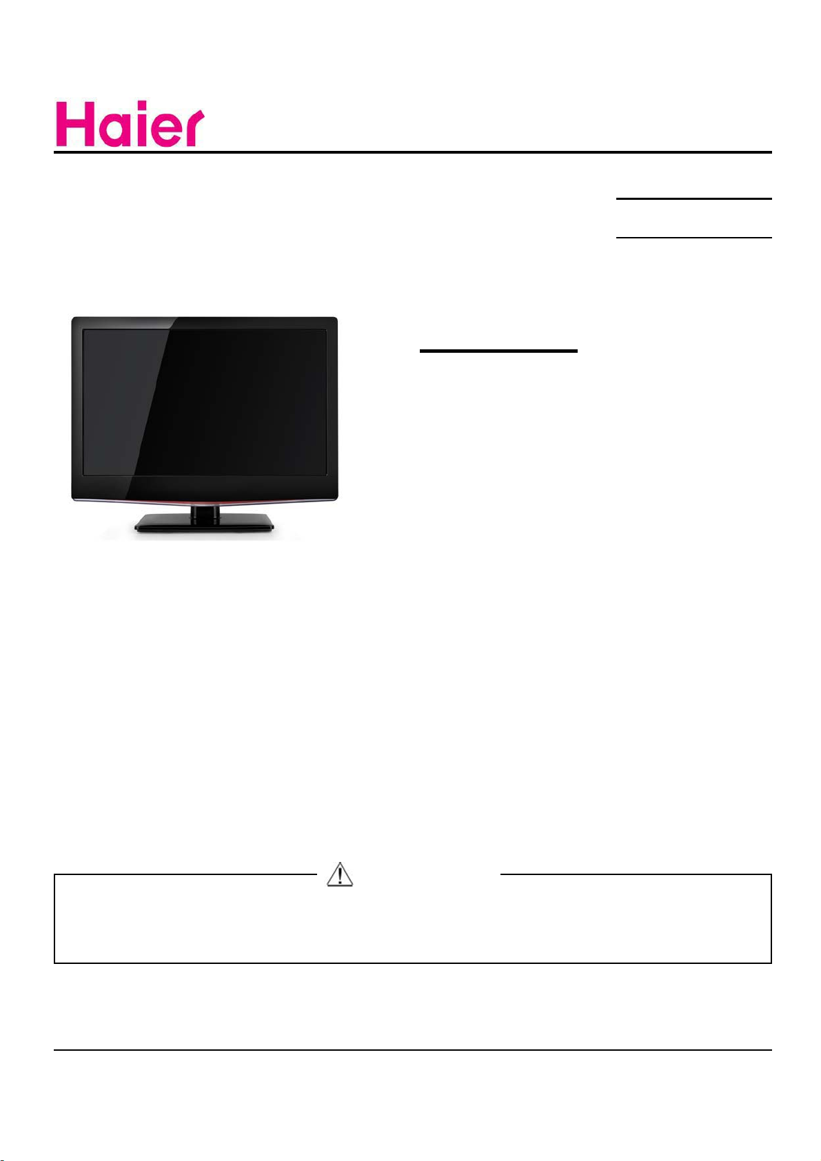
SERVICE MANUAL
LCD TV
Model No.
MSD318
LEC32B1380
LEC32B1380W
Chassis
WARNING
This service information is designed for experienced repair technicians only and is not designed for use by the general public.
It does not contain warnings or cautions to advise non-technical individuals of potential dangers in attempting to service a product.
Products powered by electricity should be serviced or repaired only by experienced professional technicians. Any attempt to service or repair
the product or products dealt with in this service information by anyone else could result in serious injury or death.
©2009 Qingdao Haier Electronics Co., Ltd.
All rights reserved. Unauthorized copying and distribution is a violation of law.
Haier Group

Chapter 1: General Information
1-1. Table of Contents
1. General Information...........................................................................
1-1. Table of Contents
1-2. General Guidelines
1-3. Important Notice
1-4. How to Read this Service Manual
6SHFL¿FDWLRQV....................................................................................
3. Location of Controls and Components...........................................
3-1. Board Location
3-2. Main Board & AV Board
3-3. Power Board
3-4. LCD Panel
4. Disassemble and Assemble..........................................................
4-1 Remove the Pedestal
4-2 Remove the Back Cover 14
4-3 Remove the Terminal Bracket
4-4 Remove the Power Module 15
1
1
3
3
6
7
88
8
8
11
12
14
14
15
4-5 Remove the Main Board 15
4-6 Remove the Speaker 16
4-7 Remove the Remote Control Board 16
5. Installation Instructions..…....………………...........………….........
5-1 External Equipment Connections 16
5-2 HDMI Connections 20
6. Operation Instructions....…....………………...........………….........
6-1 Front Panel Controls
6-2 Back Panel Controls
6-3 Universal Remote Control
7. Electrical Parts…....………………...........………….........................
7-1. Block Diagram
7-2. Circuit Diagram
7-3. Wiring Connection Diagram
8. TV Operation........………….............................................................
16
23
23
23
24
25
25
26
35
36
- 01 -

9. Trouble-shooting…………..............................................................
9-1. Simple Check 43
43
9-2. Main Board Failure Check
10.1 DVD OPERATION
11.1. Panel Failure
…………..............................................................
…………..............................................................
44
50
55
- 02 -

1-2. General Guidelines
When servicing, observe the original lead dress. If a short circuit is found, replace all parts
which have been overheated or damaged by the short circuit.
After servicing, see to it that all the protective devices such as insulation barriers, insulation
papers shields are properly installed.
After servicing, make the following leakage current checks to prevent the customer from
being exposed to shock hazards.
1) Leakage Current Cold Check
2) Leakage Current Hot Check
3) Prevention of Electro Static Discharge (ESD) to Electrostatically Sensitive
1-3. Important Notice
1-3-1. Follow the regulations and warnings
Most important thing is to list up the potential hazard or risk for the service personnel to
open the units and disassemble the units. For example, we need to describe properly
how to avoid the possibility to get electrical shock from the live power supply or charged
electrical parts (even the power is off).
This symbol indicates that high voltage is present inside.It is dangerous to
make any king of contact with any inside part of this product.
This symbol indicates that there are important operating and maintenance
instructions in the literture accompanying the appliance.
1-3-2. Be careful to the electrical shock
7RSUHYHQWGDPDJHZKLFK PLJKWUHVXOWLQ HOHFWULFVKRFNRU¿UH GRQRWH[SRVH WKLV79VHW
to rain or excessive moisture. This TV must not be exposed to dripping or splashing water,
DQGREMHFWV¿OOHGZLWKOLTXLGVXFKDVYDVHVPXVWQRWEHSODFHGRQWRSRIRUDERYHWKH79
1-3-3. Electro static discharge (ESD)
Some semiconductor (solid state) devices can be damaged easily by static electricity. Such
components commonly are called Electrostatically Sensitive (ES) Devices. The following
techniques should be used to help reduce the incidence of component damage caused by
electros static discharge (ESD).
1-3-4. About lead free solder (PbF)
This product is manufactured using lead-free solder as a part of a movement within the
consumer products industry at large to be environmentally responsible. Lead-free solder
must be used in the servicing and repairing of this product.
8VHWKHJHQHZLQJSDUWVVSHFL¿HGSDUWV
Special parts which have purposes of fire retardant (resistors), high-quality sound
(capacitors), low noise (resistors), etc. are used.
When replacing any of components, be sure to use only manufacture's specified parts
shown in the parts list.
Safety Component
Ɣ&RPSRQHQWVLGHQWL¿HGE\PDUNKDYHVSHFLDOFKDUDFWHULVWLFVLPSRUWDQWIRUVDIHW\
- 03 -

1-3-6 Safety Check after Repairment
&RQ¿UPWKDWWKHVFUHZVSDUWVDQGZLULQJZKLFKZHUHUHPRYHGLQRUGHUWRVHUYLFHDUH SXW
in the original positions, or whether there are the positions which are deteriorated around
the serviced places serviced or not. Check the insulation between the antenna terminal or
external metal and the AC cord plug blades. And be sure the safety of that.
General Servicing Precautions
1. Always unplug the receiver AC power cord from the AC power source before;
a. Removing or reinstalling any component, circuit board module or any other receiver
assembly.
b. Disconnecting or reconnecting any receiver electrical plug or other electrical
connection.
c. Connecting a test substitute in parallel with an electrolytic capacitor in the receiver.
CAUTION: A wrong part substitution or incorrect polarity installation of electrolytic
capacitors may result in an explosion hazard.
2. Test high voltage only by measuring it with an appropriate high voltage meter or other
voltage measuring device (DVM, FETVOM, etc) equipped with a suitable high voltage
probe.
Do not test high voltage by "drawing an arc".
3. Do not spray chemicals on or near this receiver or any of its assemblies.
4. Unless specified otherwise in this service manual, clean electrical contacts only by
applying the following mixture to the contacts with a pipe cleaner, cotton-tipped stick or
comparable non-abrasive applicator; 10% (by volume) Acetone and 90% (by volume)
isopropyl alcohol (90%-99% strength).
CAUTION:7KLVLVDÀDPPDEOHPL[WXUH
8QOHVVVSHFL¿HGRWKHUZLVHLQWKLVVHUYLFHPDQXDOOXEULFDWLRQRIFRQWDFWVLVQRWUHTXLUHG
Capacitors may result in an explosion hazard.
5. Do not defeat any plug/socket B+ voltage interlocks with which receivers covered by this
service manual might be equipped.
6. Do not apply AC power to this instrument and/or any of its electrical assemblies unless
all solid-state device heat sinks are correctly installed.
7. Always connect the test receiver ground lead to the receiver chassis ground before
connecting the test receiver positive lead.
Always remove the test receiver ground lead last. Capacitors may result in an explosion
hazard.
8VHZLWKWKLVUHFHLYHURQO\WKHWHVW¿[WXUHVVSHFL¿HGLQWKLVVHUYLFHPDQXDO
CAUTION: 'RQRWFRQQHFWWKHWHVW¿[WXUHJURXQGVWUDSWRDQ\KHDWVLQNLQWKLVUHFeiver.
9. Remove the antenna terminal on TV and turn on the TV.
10. Insulation resistance between the cord plug terminals and the eternal exposure metal
should be more than Mohm by using the 500V insulation resistance meter.
11. If the insulation resistance is less than M ohm, the inspection repair should be required.
If you have not the 500V insulation resistance meter, use a Tester. External exposure
metal: Antenna terminal Headphone jack
- 04 -

Electrostatically Sensitive (ES) Devices
Some semiconductor (solid-state) devices can be damaged easily by static electricity.
Such components commonly are called Electrostatically Sensitive (ES) Devices.
Examples of typical ES devices are integrated circuits and some field-effect transistors
and semiconductor "chip" components. The following techniques should be used to help
reduce the ncidence of component damage caused by static by static electricity.
1. Immediately before handling any semiconductor component or semiconductorequipped assembly, drain off any electrostatic charge on your body by touching a known
earth ground. Alternatively, obtain and wear a commercially available discharging wrist
strap device, which should be removed to prevent potential shock reasons prior to applying
power to the unit under test.
2. After removing an electrical assembly equipped with ES devices, place the assembly
on a conductive surface such as aluminum foil, to prevent electrostatic charge buildup or
exposure of the assembly.
3. Use only a grounded-tip soldering iron to solder or unsolder ES devices.
4. Use only an anti-static type solder removal device. Some solder removal devices not
FODVVL¿HGDVDQWLVWDWLFFDQJHQHUDWHHOHFWULFDOFKDUJHVVXI¿FLHQWWRGDPDJH(6GHYLFHV
'RQRWXVHIUHRQSURSHOOHGFKHPLFDOV7KHVHFDQJHQHUDWHHOHFWULFDOFKDUJHVVXI¿FLHQW
to damage ES devices.
6. Do not remove a replacement ES device from its protective package until immediately
before you are ready to install it.
(Most replacement ES devices are packaged with leads electrically shorted together by
conductive foam, aluminum foil or comparable conductive material).
7. Immediately before removing the protective material from the leads of a replacement
ES device, touch the protective material to the chassis or circuit assembly into which the
device will be installed.
CAUTION: Be sure no power is applied to the chassis or circuit, and observe all other
safety precautions.
8. Minimize bodily motions when handling unpackaged replacement ES devices.
(Otherwise harmless motion such as the brushing together of your clothes fabric or the
OLIWLQJRI\RXUIRRWIURPDFDUSHWHGÀRRUFDQJHQHUDWHVWDWLFHOHFWULFLW\VXI¿FLHQWWRGDPDJH
an ES device.)
1-3-7. Ordering Spare Parts
Please include the following informations when you order parts. (Particularly the Version
letter)
1. Model number, Serial number and Software Version
The model number and Serial number can be found on the back of each product and the
Software Version can be found at the Spare Parts List.
2. Spare Part No. and Description
<RXFDQ¿QGWKHPLQWKH6SDUH3DUWV/LVW
- 05 -

1-3-8. Photo used in this manual
The illustration and photos used in this Manual may not base on the final design of
products, which may differ from your products in some way.
1-4. How to Read this Service Manual
Using Icons:
,FRQVDUHXVHGWRDWWUDFWWKHDWWHQWLRQRIWKHUHDGHUWRVSHFL¿FLQIRUPDWLRQ7KHPHDQLQJRI
each icon is described in the table below:
Note:
A “note” provides information that is not indispensable, but may nevertheless be valuable
to the reader, such as tips and tricks.
Caution:
A “caution” is used when there is danger that the reader, through incorrect manipulation,
may damage equipment, loose data, get an unexpected result or has to restart(part of) a
procedure.
Warning:
A “warning” is used when there is danger of personal injury.
Reference:
A “reference” guides the reader to other places in this binder or in this manual, where he/
VKHZLOO¿QGDGGLWLRQDOLQIRUPDWLRQRQDVSHFL¿FWRSLF
- 06 -

Service Manual
Model No.:
2. Speci¿cations
Model LEC32B1380/LEC32B1380W
Screen Size 32 inch
Aspect Ratio 16:9
x
Resolution 1920*
1080
Response Time (ms)
Angel of View
Color Display 16777216
No. of Preset Channels
OSD Language English
Color System NTSC/PAL/SECAM
Audio System NTSC
Audio Output Power
(Built-in) (W)
Audio Output Power
(outer) (W)
Total Power Input (W) 90 W
Voltage Range (V)
6.5 (GRAY TO
GRAY)
+88/-88(H), +88/-88
(V) Typ.
Cable :1-135/ Air:
2-69(ATV&DTV)
8W×2
No
AC 100-240V
Power Frequency (Hz) 50~60Hz
Net Weight (KG)
Gross Weight (KG)
Net Dimension (MM)
Packaged Dimension
8.1
9.5
775*180*537
864*125*595
(MM)
- 07 -
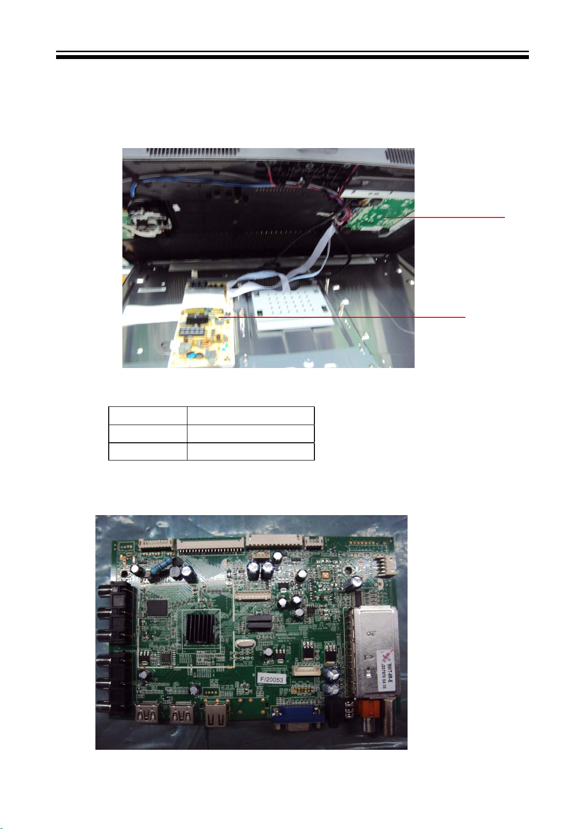
3. Location of Controls and Components
3-1 Board Location
A Board
B Board
No. Description
A Board Main Board
B Board Power Board
3-2 Main Board
- 08 -

3-2-1 Function Description:
Main Board
Process signal which incept from exterior equipment then translate into signal that panel
can display.
3-2-2 Connector defnition
Main board connector
Power connectors (J15ˈ
J16
J16
1
2
3
4
5
+5V
BL-ON/OFF
BL-ADJUST
+5V
GND
Pin number Signal name
1 GND
2
3 +5V
4 +5V
J15
GND
5 POWER ON/OFF
6 +5VSTB
7 +5V
8 +5V
9 GND
10 GND
11 GND
12 +12V
13 +12V
Notes:
J16-Pin 2: Backlight on/off:
The system c an turn o n or turn o ff t he backlight of TFT LCD P anel through the power
supply unit path.
System board will use this pin to control system power.
J16-Pin 3: Control the luminance of backlight
The system can generate the PWM s ignal to control the strength of T FT LCD Panel’s
backlight through this connector
- 09 -

Keypad and remote connector (J12)
Pin number Signal name Description
1 LED_R LAMP RED
2 LED_G LAMP GREEN
3
4 IR REMOTE CONTROL
5 GND GND
6 5V POWER FOR REMOTE
7
8 KEY1
9 KEY0
10 GND
Speaker connector J11
Pin number Signal nameD escription
+KPSR+KPSR1
-KPSR-KPSR2
-KPSL-KPSL3
+KPSL+KPSL4
3-3. Power Board
- 10 -

3-3-1 Function Description:
Supply power for Main board, Panel.
&RQQHFWRUGH¿QLWLRQ
CN1
Pin number Signal name
GND
GND
5
6
7
8
+24V
+24V
+24V
+24V
CN2
Pin number Signal name
GND
POWER ON/OFF
+5VSTB
GND
+5V
GND
+5V
GND
9 GND
10 GND
11 GND
12 +12V
3-4. LCD Panel
13 +12V
V315H4-LE2
- 11 -

3-4-1 Function Description: Display the signal.
&RQQHFWRUGH¿QLWLRQ
Pin Name Description Note
1 GND Ground
2
N.C.
3
N.C.
4 N.C. No Connection
5 N.C. No Connection
6 N.C. No Connection
7
SELLVDS LVDS data format Selection
8
N.C. No Connection
9
N.C. No Connection
10 N.C. No Connection
11 GND Ground
12
ERX0- Even pixel Negative LVDS differential data input. Channel 0
13
ERX0+ Even pixel Positive LVDS differential data input. Channel 0
14
ERX1- Even pixel Negative LVDS differential data input. Channel 1
15
ERX1+ Even pixel Positive LVDS differential data input. Channel 1
16
ERX2- Even pixel Negative LVDS differential data input. Channel 2
17
ERX2+ Even pixel Positive LVDS differential data input. Channel 2
18
GND Ground
19
ECLK- Even pixel Negative LVDS differential clock input.
20
ECLK+ Even pixel Positive LVDS differential clock input.
21
GND Ground
22
ERX3- Even pixel Negative LVDS differential data input. Channel 3
23
ERX3+ Even pixel Positive LVDS differential data input. Channel 3
24 N.C. No Connection
25 N.C. No Connection
26 GND Ground
27 GND Ground
28
ORX0- Odd pixel Negative LVDS differential data input. Channel 0
29
ORX0+ Odd pixel Positive LVDS differential data input. Channel 0
30
ORX1- Odd pixel Negative LVDS differential data input. Channel 1
31
ORX1+ Odd pixel Positive LVDS differential data input. Channel 1
32
ORX2- Odd pixel Negative LVDS differential data input. Channel 2
33
ORX2+ Odd pixel Positive LVDS differential data input. Channel 2
34
GND Ground
35
OCLK- Odd pixel Negative LVDS differential clock input
36
OCLK+ Odd pixel Positive LVDS differential clock input
37
GND Ground
38
ORX3- Odd pixel Negative LVDS differential data input. Channel 3
39
ORX3+ Odd pixel Positive LVDS differential data input. Channel 3
40
N.C.
41 N.C. No Connection
42 GND Ground
No Connection
No Connection
No Connection
(2)
(3)(4)
(2)
(5)
(5)
(5)
(2)
(5)
(5)
(5)
(2)
- 12 -

43 GND Ground
44 GND Ground
45 GND Ground
46 GND Ground
47 N.C. No Connection
48
VCC Power input (+12V)
49
VCC Power input (+12V)
50
VCC Power input (+12V)
51
VCC Power input (+12V)
Note (1) LVDS connector pin order defined as follows.
(2)
Note (2) Reserved for internal use. Please leave it open.
Note (3) Low = Open or connect to GND: VESA Format, High = Connect to +3.3V: JEIDA Format.
Note (4) LVDS signal pin connected to the LCM side has the following diagram. R1 in the system side should be
less than 1K Ohm. (R1 < 1K Ohm)
TCON
TCON
R2
R1
R1
Selector (pin7)
System side
Note (5) Two pixel data send into the module for every clock cycle. The first pixel of the frame is odd pixel and
the second pixel is even pixel
R2
R3
R3
Setting
Setting
LCM side
LCM sideSystem side
- 13 -

4. Disassemble and assemble
4-1 Remove the Pedestal 4-3. Remove the adhesive tape
(The location of the adhesive tape as follows)
/D\GRZQWKHXQLWVRWKDWUHDUFRYHU
faces upward
5HPRYHWKHIRXUVFUHZIURPWKH
UHDUFRYHULQGLFDWHGZLWKż
7KHQUHPRYHWKHSHGHVWDO
4-2Remove the Back Cover
Remove the adhesive tape indicated on the
¿JXUHDERYH
5HPRYHWKHWKHVHVFUHZLQGLFDWHGRQ
¿JXUHDERYHE\ż
7KHQUHPRYH WKHEDFNFRYHUIURPWKH
unit.
- 14 -

4-3 Remove the Terminal Bracket
4-4 Remove the power module
5HPRYHWKHIRXUVFUHZLQGLFDWHGRQWKH
¿JXUHDERYHE\ż
7KHQUHPRYHWKHSRZHUPRGXOH
4-5 Remove the Main board
5HPRYHWKHWZRVFUHZLQGLFDWHG
RQWKH¿JXUHDERYHE\ż
'LVFRQQHFWHGWKHFRXSOHU
J16 J12 J9 J15 J11 J5 J3
5HPRYHWKH0DLQERDUG
- 15 -
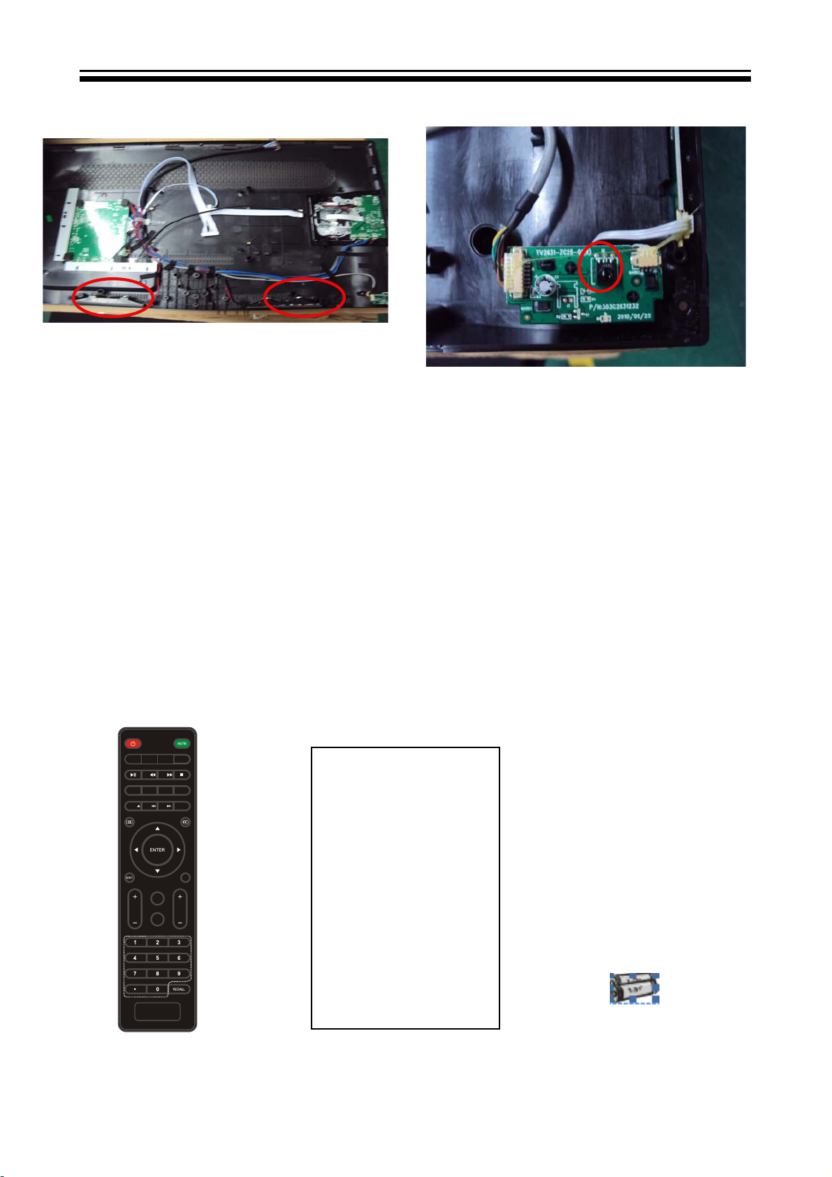
4-6 Remove the speaker
4-7 Remove the remote control
Take out the speaker
5. Installation Instructions
5-1 External Equipment Connections
Accessories
RETURN DISPLAY AUDIO SUBTITLE
MTS/
CC/
MENU
REPEAT
CH LIST/
SETUP
GOTO
FAV/
ASPECT
EPG/
take out the remote
control board
TV
DISPLAY
S.M
VOL
CH
P.M
Remote Control
User GUIDE
- 16 -
Battery

- 17 -
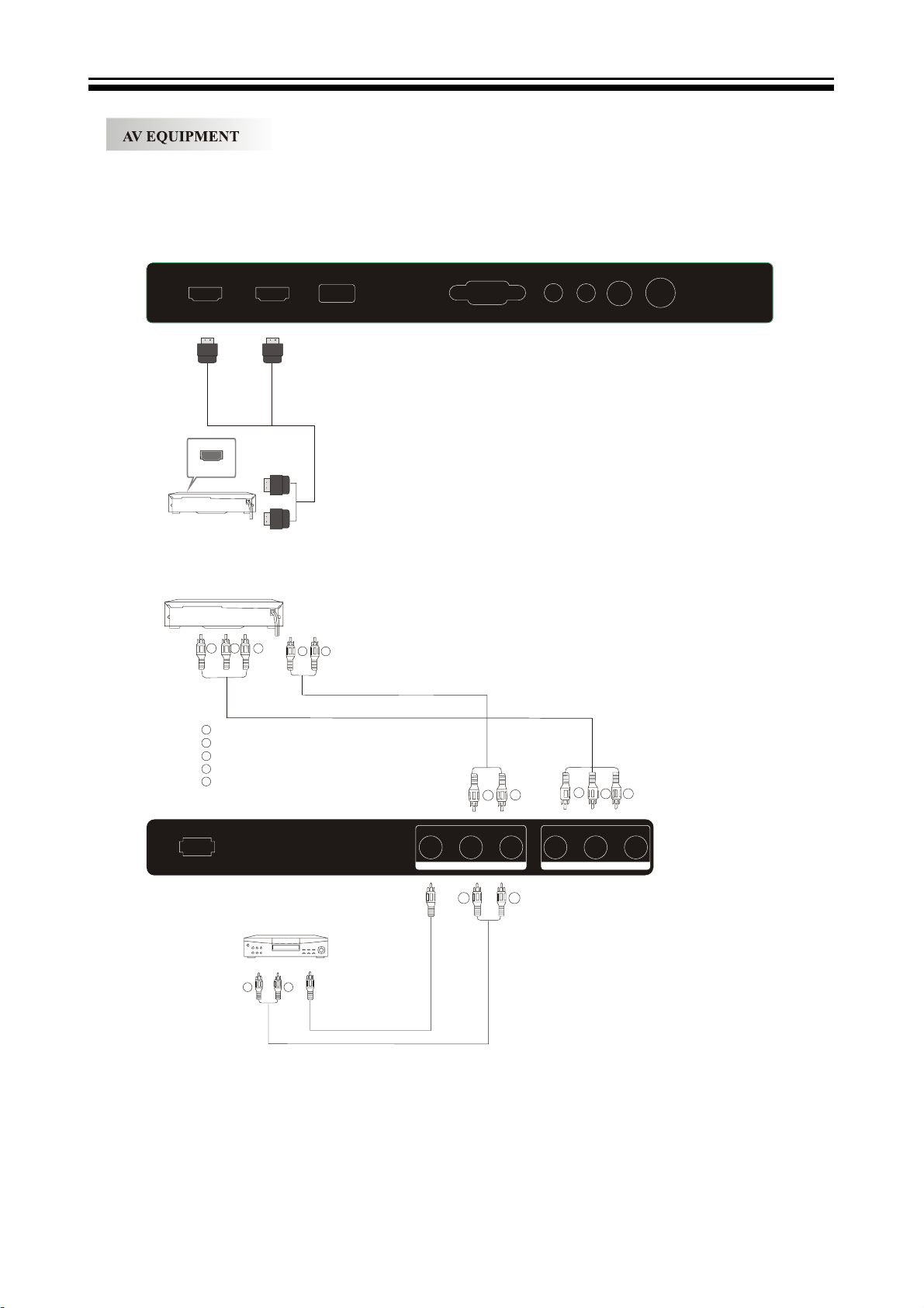
You can use the input terminals on TV set rear as follows.
HDMI1
HDMI1
HDMI
VIDEO EQUIPMENT with YPbPr
G
Y
W
R
B
G
HDMI2
R
B
Yellow (video)
White(audio L)
Red(audio R or Pr)
Blue(Pb)
Green(Y)
USB
W
R
VGA
W
HEADPHONERFPC AUDIO
R
COAXIAL
G
R
B
AC-INPUT
100-240V~50/60Hz
VIDEO
LR
COMPOSITE
YPbPr
COMPONENT
W R
VIDEO EQUIPMENT
W R
TO AUDIO OUTPUTS
TO VIDEO
OUTPUTS
The television's inputs can be connected to the following types of equipment: VCR, multi disc player,
DVD, camcorder, video game or stereo system, etc.....
YPbPr can support these video formats:480i,576i,480p,576p,720p,1080i.
- 18 -

PC
STEPS:
Be sure both the TV and computer are set to
Power off.
1.Connect VGA and audio cable.
2.Connect the power cord.
3.Power on the TV, switch to PC mode.
4.Power on the PC.
This sequence is very important.
VGA
HDMI1 HDMI2
USB
HEADPHONERFPC AUDIO COAXIAL
PRESET MODE
RESOLUTION
1
2
3
4
5
6
7
8
9
10
720*400
640*480
640*480
800*600
800*600
1024*768
1024*768
1024*768
1280*1024
1280*1024
V.Freq.(Hz) H.Freq.(KHz)
70
60
75
60
75
60
70
75
60
75
31.47
31.47
37.50
37.88
46.88
48.36
56.48
60.02
63.98
80.00
- 19 -

5-2 HDMI Connections
When the source device supports HDM
How To Connect
1. Connect the source device to HDMI port of this TV with an HDMI cable(not supplied
with this product).
2. No separated audio connection is necessary.
How To Use
If the source device supports Auto HDMI function, the output resolution of the source
device will be automatically
set to 1280x720p.
If the source device does not support Auto HDMI, you need to set the output resolution
appropriately.
To get the best picture quality, adjust the output resolution of the source device to
1280x720p.
Select HDMI input source in input source option of Select Main source menu.
When the source device supports DVI
How To Connect
1. Connect the source device to HDMI port of this TV with a HDMI-to-DVI cable(not
supplied with this product).
2. A separated audio connection is necessary.
3. If the source device has an analog audio output connector, connect the source device
audio output to DVI Audio In port located on the PC port.
How To Use
If the source device supports Auto DVI function, the output resolution of the source device
will be automatically
set to 1280x720p.
If the source device does not support Auto DVI, you need to set the output resolution
appropriately.
To get the best picture quality, adjust the output resolution of the source device to
1280x720p.
Press the INPUT button to select HDMI input source in input source option of Select Main
source menu.
Installation
- 20 -
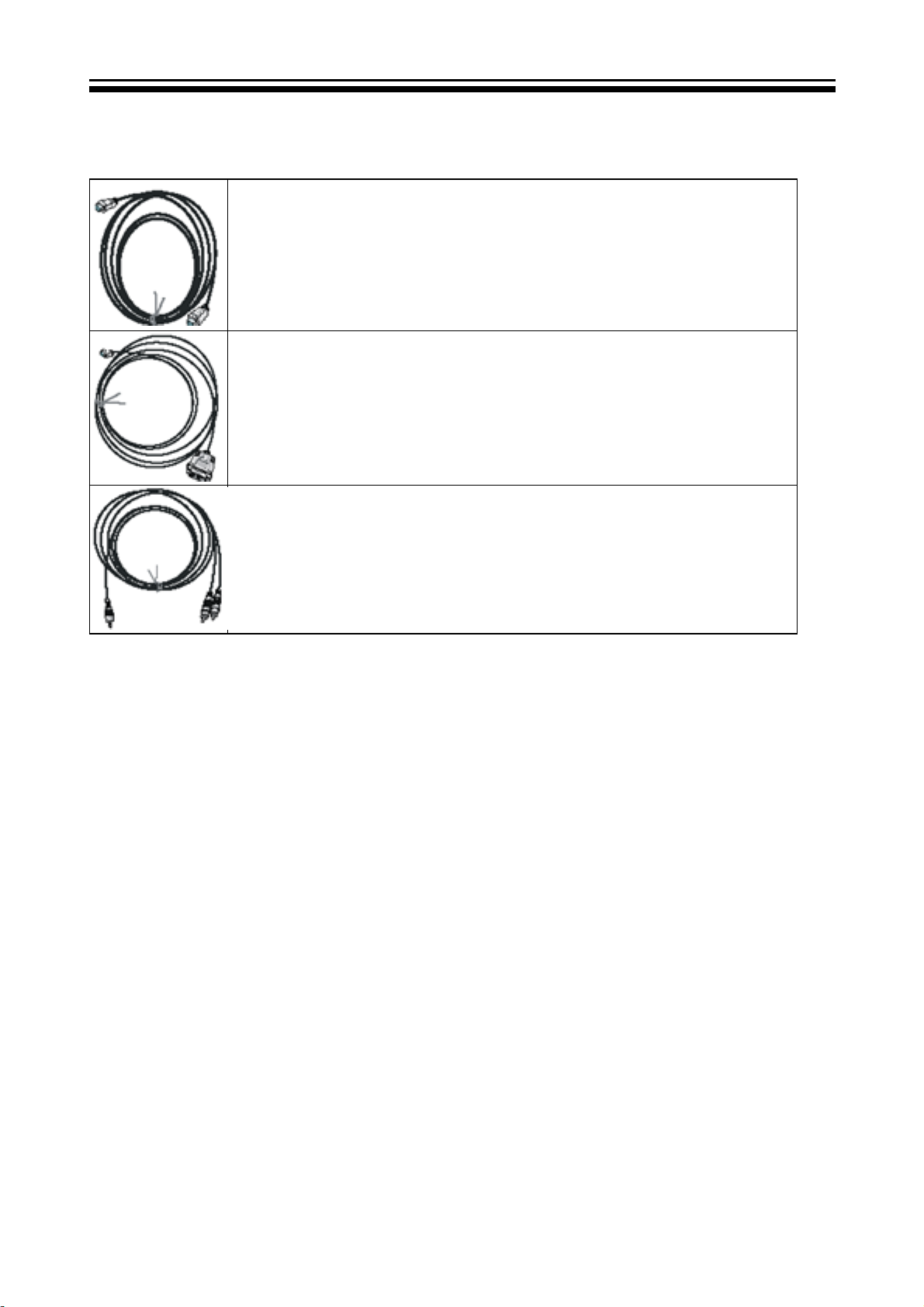
Cable sample
HDMI Cable
(not supplied with the product)
HDMI to DVI Cable
( not supplied with the product)
Analog Audio Cable
(Stereo to RCA type)
(not supplied with the product)
Connecting Headphones
You can connect a set of headphones to your set if you wish to watch a
TV programmer without disturbing the other people in the room.
- 21 -

TO USE AC POWER SOURCE
Use the AC polarized line cord provided for operation on AC.
Insert the AC cord plug into a standard polarized AC outlet.
NOTES:
Ŷ1HYHUFRQQHFWWKH$&OLQHFRUGSOXJWRRWKHUWKDQWKHVSHFL¿HGYROWDJH
Use the attached power cord only.
Ŷ,IWKHSRODUL]HG$&FRUGGRHVQRW¿WLQWRDQRQSRODUL]HG$&RXWOHW
GRQRWDWWHPSWWR¿OHRUFXWWKHEODGH,WLVWKHXVHUCVUHVSRQVLELOLW\WRKDYHDQ
electrician replace the obsolete outlet.
Ŷ,I\RXFDXVHDVWDWLFGLVFKDUJHZKHQWRXFKLQJ WKH XQLW DQG WKH XQLW IDLOV WRIXQFWLRQ
simply unplug the unit from the AC outlet and plug it back in. The unit should return to
normal operation.
- 22 -
6. Operation Instructions
Basal information
6-1 Front panel controls
1. SOURCE: Display the input source menu.
2. MENU: Display main MENU.
3. CH+/CH-: In TV mode, press "CH+" or "CH-" to
change the channel up and down. In MENU mode, press
"CH+" or "CH-" to select items in standby mode, press
"CH+" or "CH-" to turn on the TV.
4. VOL+/VOL-: Adjust sound level. In MENU mode,
press "VOL+ " or "VOL- " to adjust the item that you
selected.
5. STANDBY: Press this button to turn the unit ON
from STANDBY mode. Press it again to turn the set
back to STANDBY.
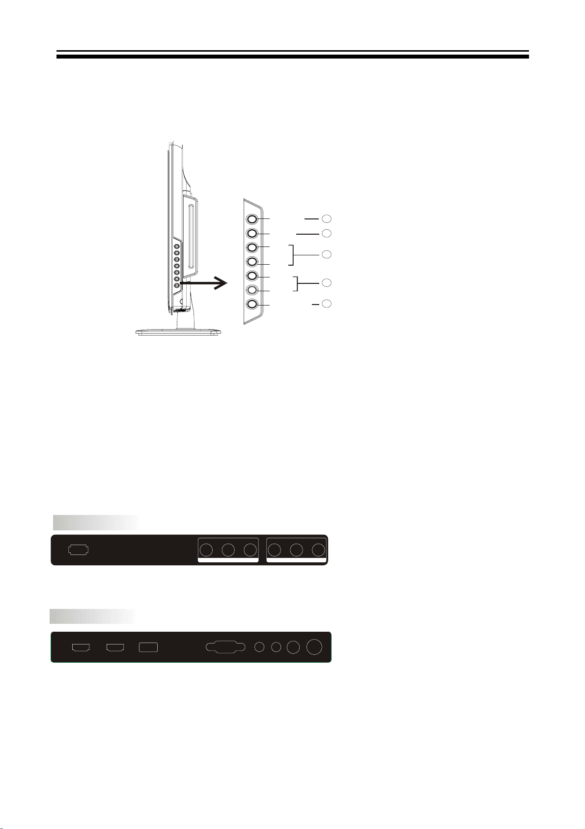
6.2 Back panel controls
SOURCE
MENU
CH+
CH-
VOL+
VOL-
STANDBY
1
2
3
4
5
REAR Connections
VIDEO
AC-INPUT
100-240V~50/60Hz
All the terminals are (from left to right):
POWER SOCKET, VIDEO, AUDIO INPUT, YPbPr INPUT
Note: AV and YPbPr share one audio channel.
LR
COMPOSITE
YPbPr
COMPONENT
SIDE Connections
HDMI1 HDMI2
All the terminals are (from left to right):
HDMI1, HDMI2, USB, VGA, HEADPHONE, PC AUDIO, COAXIAL, RF.
Note: 1. When HDMI1 has an input signal coming from a DVI source then the audio input signal must be
connected to the PC audio input.
2. When HDMI2 has an input signal coming from a DVI source then the audio input signal must be
connected to
USB
VGA
HEADPHONERFPC AUDIO
COAXIAL
- 23 -
1
27
28
23
19
21
22
16
17
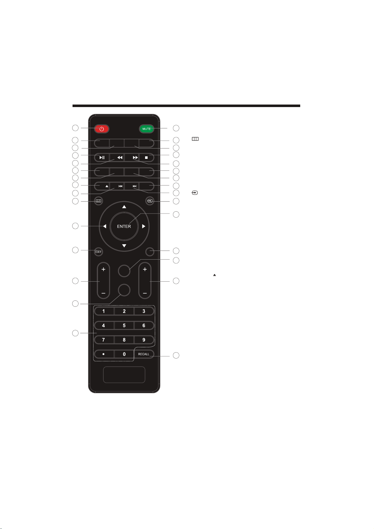
RETURN DISPLAY AUDIO SUBTITLE
MTS/
CC/
GOTO
EPG/
MENU
FAV/
SETUP
ASPECT
REPEAT
CH LIST/
3 8
4
5
S.M
6
VOL CH
P.M
DISPLAY
TV
7
REMOTE CONTROL
1: POWER
To set the TV standby or on.
9
2: NUMBER KEY
For direct access to program.
3:
29
Displays the main on-screen menu.
30
4: CURSOR
To move within the menu.
25
5: EXIT
Used to exit menu.
20
6: VOL+/VOL-
24
To adjust sound level.
7:
P.M
26
Press repeatedly to select a picture mode: Vivid, Standard,
15
Sports, Movie, or Custom.
8:
18
Press to display and select the available video sources.
9: MUTE
To disable or enable the sound.
10: RECALL
11
To access the previously viewed program.
11: ENTER
Confirms selection.
12: TV DISPLAY
Displays/removes the program Information
13:
S.M
Press repeatedly to switch audio modes: Standard, News,
Music,Theater, Sports or Custom.
12
14: CH+/CH To access the next or previous Program.
13
15: ASPECT
To change picture aspect .
16: CH LIST /
Used to display the channel list / Eject or Insert the disc.
14
17: EPG
Display all the information of DTV programs.
18: FAV
Used to access your favorite channels in digital TV mode.
19: CC
Enable or disable the CC function.
20: MTS
Switch the sound stereo.
2
10
For a description of the DVD player function buttons
on the remote, please refer to page 20 of this manual.
- 24 -

7. Electrical parts
7-1. Block diagram
12
Headphone
MSD318QT
Main IC
Coaxial
AMP
- 25 -

7-2. Circuit Diagram
1
-- --
0x210x2001
0x230x221
IPOD_SV-Cin 4
I2C ADDR
Write Read
C32 47nFC32 47nF
33R
33R
R98
R98
R124 75RR124 75R
R125 75RR125 75R
I2C slave
SPI slave
Mode
IPOD_C
MODE0
CP_RESET 4
R1671KR167
1K
1
R1631KR163
1K
RESET_CP
13
14
2 3
Q9
3904Q93904
+3.3V
0
pin Communication
0
1
MODE1
+3.3V
C504
0.1uF
C504
0.1uF
RESET_CP
R903
R903
C503 0.1uFC503 0.1uF
U25
U25
22
GND
6
7
8
9
10
23
3
5
VCC
NC3
NC4
NC5
NC7
NC8
GND
VSS11I2C_SCL12I2C_SDA13MODE014NC9
4
NRESET
2
NC2
MODE1
1
15
10K
10K
NC1
GND
NC14
NC13
NC12
NC11
NC10
GND
24
21
20
19
18
17
16
NC/CP_2.0B
NC/CP_2.0B
22K
22K
IPOD_CVBS_IN 4
C66 560pFC66 560pF
R96 33RR96 33R C30 47nFC30 47nF
R127 12KR127 12K
IPOD_CVBS
IPOD_TX 4
IPOD-Rin 4
IPOD-Lin 4
C5262.2uF C5262.2uF
C5272.2uF C5272.2uF
C48 560pFC48 560pF
2
R126 12KR126 12K
R115
R115
R114
22K
R114
22K
IPOD_IN_L
IPOD_IN_R
3
4
+5V
113355779
224466881010121214
CN8 DIP-14(2*7)CN8 DIP-14(2*7)
IPOD_SV-Yin 4
C31 47nFC31 47nF
R97 33RR97 33R
R123 75RR123 75R
IPOD_Y
+3.3V
IPOD_DETECT 4
+3.3V
IPOD_RX 4
R919 10KR919 10K
R918 100RR918 100R
9
111113
Date: Feb. 3,2010
TITLE: IPOD IF
1
APPRD:
2
CHECKED:
SHEET: 9 OF 9 VER:1.0
DESIGN:George Guo
MODEL: MSAV3207-K3
3
4
5
IPOD_Y
D D
IPOD_C
IPOD_CVBS
IPOD_IN_R
IPOD_IN_L
C C
R901 100RR901 100R
I2C-SCL4
R902 100RR902 100R
I2C-SDA4
MODE0 MODE1
B B
R905
R905
100R
100R
A A
5
- 26 -

Date: Feb. 3,2010
IF+
IF-
LS16
220nH
LS16
220nH
CS31
39pF
CS31
U28
U28
NC/1K
NC/1K
IF- 4
IF-
11
120ohm_FB
120ohm_FB
AIF
D D
FSA3157P6X
FSA3157P6X
0.1uF
0.1uF
CS5
CS5
12
AIF
Close Silicon Tuner
VIFN_OUT
CS34 10nFCS34 10nF
123
B1
B1
GND
GND
S
VCC
S
VCC
5
6
IFS1
0.1uF
0.1uF
LS5
LS5
LS4
LS4
LS3
LS3
CS4
CS4
1nF
1nF
CS3
CS3
0.1uF
0.1uF
C150
20pF
C150
20pF
C149
20pF
C149
20pF
GND13GND14GND15GND
R216 100RR216 100R
C262 4700pFC262 4700pF
B0
B0
A
A
4
3.3VCC_T
16
3.3VCC_TM
U29
U29
1.8VCC
39pF
VIFP_OUT
CS35 10nFCS35 10nF
123
B1
B1
FSA3157P6X
FSA3157P6X
S
S
6
IFS2
4700pF
4700pF
CS8
CS8
CS7
CS7
120nH
120nH
33nH
33nH
3.6nH
3.6nH
120ohm_FB
120ohm_FB
LS6
LS6
0R
RS50RRS5
Vdd_A1.6V
10K
10K
RS3
RS3
1M
RS61MRS6
CS33
10nF
CS33
10nF
25
26
27
28
29
30
31
32
33
1
2
R217 100RR217 100R
C263 4700pFC263 4700pF
B0
B0
GND
GND
A
A
VCC
VCC
4
5
4700pF
4700pF
24
22
23
IF_OUTP
IF_OUTN
VAGC1
IF_OUTP2
VBATT_A2
VREG_A_OUT2
TF_3
TF_2
VDD_DNX1
TF_1
PADDLE
LNA_IN2AS6IDAC3VDD_DNX21VBATT_A34VAGC25VBATT_A57XTAL_N
U4
U4
CS9
0.1uF
CS9
0.1uF
NC
LS8
12nH
LS8
12nH
RS7NCRS7
3.3VCC_T
CS10
56pF
CS10
56pF
LS7
LS7
CS14
27pF
CS14
27pF
DS1
BAV99
DS1
BAV99
CS13
39pF
CS13
39pF
3
RS81MRS8
CS12
CS12
4
789
75 ohm Line
1
256
F Conn
F Conn
JS1
JS1
T_RF_AGC RF_AGC
RF AGC Switch
IFS1
RS211KRS21
RF_AGC_SEL
Vdd_A1.6V_D
3.3VCC_T
Vdd_A1.6V_D
LS12 120ohm_FBLS12 120ohm_FB
LS10 120ohm_FBLS10 120ohm_FB
RS9 47RRS9 47R
21
20
IF_OUTN2
VBATT_A4
VDD_REF_SX
MXL302RF_V8_F1_32
MXL302RF_V8_F1_32
CS17
CS17
LS9 120ohm_FBLS9 120ohm_FB
CS18
82pF
CS18
82pF
330nH
330nH
LS11
LS11
220nH
220nH
CS16
180pF
CS16
180pF
1M
1nF
1nF
10
3
RF Input
Port
LNA GND
Q59
3906
Q59
3906
R440
R440
R438
R438
5V-Tuner
IFS2
1K
1K
RS221KRS22
3.3VCC_T
LS13 120ohm_FBLS13 120ohm_FB
CS19
0.1uF
CS19
0.1uF
CS20
2.2uF
CS20
2.2uF
19
18
17
F1
F1
VDD_IO
GND_DIG
SDA
VREG_D_IN
VREG_D_OUT
SCL
VBATT_A1
VREG_A_OUT1
GND_XTAL
CLK_OUT
XTAL_P
8
NC
RS10NCRS10
Put on digital GND plane
0.1uF
0.1uF
Vdd_RF_VCO_LO_3V
RF_AGC_SEL 4
100K
100K
10K
10K
R437
R437
10K
10K
Q58
Q58
16
15
14
13
12
11
10
9
RS12NCRS12
Vdd_A1.6V_D
3904
3904
RS15
RS15
RS14
RS14
3.3VCC_T
NC
C C
4.7K
4.7K
4.7K
4.7K
RS16
RS16
Vdd_IO
RS13 0RRS13 0R
100R
100R
3.3VCC_T
RS24NCRS24
T_SDA
T_SCL
CS24
CS24
CS23
CS23
RS17
RS17
3.3VCC_T
SSDA
SSCL
LS15 120ohm_FBLS15 120ohm_FB
CS22
CS22
RS18 120RRS18 120R
LS14 120ohm_FBLS14 120ohm_FB
US1
US1
OUT
OUT
ADJ
ADJ
NC
For silicon tuner
R282
NC/1K
R282
NC/1K
18PF
18PF
18PF
18PF
100R
100R
0.1uF
0.1uF
AMS1117-3.3
AMS1117-3.3
IN
IN
+3.3V_SB
+5V
US2
AMS1117-ADJ
US2
AMS1117-ADJ
0.1uF
0.1uF
CS36
CS36
3
IN
IN
214
OUT
OUT
ADJ
ADJ
RS261KRS26
1K
CS26
2.2uF
CS26
2.2uF
12
Y2
24.000MHZY224.000MHZ
CS27NCCS27
RS19 0RRS19 0R
+
+
+5V
CS25
CS25
3
214
RS250RRS25
0R
3.3VCC_T
DEMOD_IF_AGC 4
R2761KR276
1K
R279
10K
R279
10K
C143
0.1uF
C143
0.1uF
IF-5V
R281
10R
R281
10R
C139
C139
IFAGC
+5V
RS27
470R
RS27
470R
1.8VCC+1.8V
NC
RS23NCRS23
Vdd_A1.6V_D
NC
100uF/16V
100uF/16V
0.1uF
0.1uF
CS29
CS29
CS28
CS28
100uF/16V
100uF/16V
Important:
D_RF_AGC 4
R283
NC/0R
R283
NC/0R
R278
10K
R278
10K
R280
10K
R280
10K
IF-5V
Closed to MstIC
22nF
22nF
C142
22nF
C142
22nF
RF_AGC
0.1uF
0.1uF
CS32
CS32
CS39
CS39
100uF/16V
100uF/16V
J1J1
J21J21
J13J13
Analog GND and digital GND is still separate,
but through Paddle GND connecting them,
please talk to SYU if anything not understood
If use single saw filter(internal),
Delete R276,R280
Add R283(0R)
Delete Q59
Delete C73
B B
SIF_IN- 4
SIF_IN+ 4
4
5
OUT1
OUT2
GND
M9370M
M9370M
SAW
SAW
ING
IN
U22
U22
2
1
SIFP_OUT+
SIFP_OUT-
R2900RR290
0R
C214 10nFC214 10nF
L7
NC/1uHL7NC/1uH
R139
R139
NC/680R
NC/680R
R141
NC/4.7K
R141
NC/4.7K
C72
NC/15nF
C72
NC/15nF
C71
NC/10uF
C71
NC/10uF
NC/100R
NC/100R
R138
R138
+8V
5V-Tuner
FB5
FB5
FB56R/1A
FB56R/1A
5.19V 116mA (ATV)
Vpp
80mv
2
VOUT
4
+5V_LDO
VIN
3
Vpp
80mv
+8V
2
VOUT
4
AMS1084CD-ADJ
AMS1084CD-ADJ
VIN
3
+12V
3
R2880RR288
R154
R154
ADJ1TAB
C82
C82
R153
R153
ADJ1TAB
VIFN_OUT
VIFN_OUT
0R
3
1
AGND
C73
C73
AIF
220R
220R
U12
AMS1084CD-ADJ
U12
AMS1084CD-ADJ
10uF
10uF
150R
150R
U13
U13
C25
0.1uF
C25
0.1uF
C221 0.1uFC221 0.1uF
3
Q12
Q12
C559
C559
C8
EC6
+
EC16
+
VIF_M 4
4
OUT1
ING
2
2
NC/2SC2216
NC/2SC2216
R137
R137
0.1uF
0.1uF
0.1uFC80.1uF
470uF/16V+EC6
470uF/16V
C74
C74
470uF/16V+EC16
470uF/16V
L3
NC/56R
NC/56R
10nF
10nF
10uF
10uF
L4
GND
NC/2.2uHL3NC/2.2uH
NC/2.2uHL4NC/2.2uH
R150
R150
R140
R140
R156
R156
C83
C83
NC/39R
NC/39R
NC/22R
NC/22R
R157
R157
0.1uF
0.1uF
820R
820R
C222 0.1uFC222 0.1uF
5
SAW
SAW
OUT2
IN
1
VIFP_OUT
VIFP_OUT
C220
10nF
C220
10nF
R271
R271
NC/1.5K
NC/1.5K
C84
C84
VIF_P 4
U23
U23
M3953M
M3953M
R1510RR151
0.1uF
0.1uF
680R
680R
A A
1
SIFP_OUT+
SIFP_OUT-
CS30 10nFCS30 10nF
CS6 10nFCS6 10nF
RS4 391RRS4 391R
RS2 391RRS2 391R
+5V
C20
2
3.3VCC_T
3
4
5
C20
IFAGC
T_RF_AGC
RS20
RS20
RS1
RS1
100R
100R
CS1
CS1
LS1
LS1
0.1uF
0.1uF
CS2
CS2
2.2uF
2.2uF
120ohm_FB
120ohm_FB
Vdd_A1.6V
LS2
LS2
1.8VCC
301RF V7 MM 301RF V8 302RF V8
Pin 1 R23 0 DNP DNP
Pin 1 R24 DNP 0 0
TUNER_I2C_SCL 4
TUNER_I2C_SDA 4
IF+ 4
IFAGC
R532 47RR532 47R
R533 47RR533 47R
R534 100RR534 100R
IF_AGC
T_SDA
IF+
T_SCL
T_RF_AGC
5V-Tuner
7
5
4
6
8
9
2
3
1
B2
BT
AS
NC
+5V
SCL
SDA
DIF210DIF1
IF-AGC
RF-AGC
U24 DA58GT-13-EU24 DA58GT-13-E
APPRD:
1
CHECKED:
SHEET: 8 OF 9 VER:1.0
DESIGN:George Guo
MODEL: MSAV3207-K3
TITLE: TUNER
2
If use single saw filter(internal),
Delete these parts of this area
0R
3
4
5
- 27 -

1
Lout1/2# to subwoofer
RLout1/2 to speaker
AL1/2 in for subwoofer
2
LOUT+
LOUT-
C706
NC/1nF
C706
NC/1nF
C709
NC/1nF
C709
NC/1nF
AL/R in for speaker
FB701
NC/FB/1206
FB701
NC/FB/1206
FB702
NC/FB/1206
FB702
NC/FB/1206
+12V
C733 NC/220nFC733 NC/220nF
C730 NC/220nFC730 NC/220nF
22
23
24
26
21
25
28
BSPL
BSNL
PGND
OUTPL
PVCCL27PVCCL
OUTNL
SD1FAULT2LINP3LINN4AGND8AVCC7GAIN16GAIN05GVDD9PLIMIT10RINN11RINP
U19
TPA3110D2
U19
TPA3110D2
+12V
GAIN1
GAIN0
AL1-
C720 NC/1uFC720 NC/1uF
R788 NC/1KR788 NC/1K
C752 NC/1uFC752 NC/1uF
MUTE MUTE#
AL+
C751 NC/1uFC751 NC/1uF
ROUT+
C735 NC/220nFC735 NC/220nF
BSNR
C707
C707
FB703 NC/FB/1206FB703 NC/FB/1206
20
C726 NC/1uFC726 NC/1uF
Date: Feb. 3,2010
APPRD:
ROUT-
NC/1nF
NC/1nF
C713
NC/1nF
C713
NC/1nF
FB704 NC/FB/1206FB704NC/FB/1206
+12V
C734 NC/220nFC734 NC/220nF
17
18
16
15
19
BSPR
PGND
OUTPR
PVCCR
PVCCR
OUTNR
GND
29
NC13PBTL
12
14
AR1-
R789
NC/10K
R789
NC/10K
R755
NC/0R_0805
R755
NC/0R_0805
R790 NC/10KR790 NC/10K
C727 NC/1uFC727 NC/1uF
C753 NC/1uFC753 NC/1uF
AR+
C750 NC/1uFC750 NC/1uF
+3.3V_SB
R365
NC/10K
R365
NC/10K
GAIN0
R364
NC/10K
R364
NC/10K
VOLUME
R3660RR366
R363
10K
R363
10K
GAIN1
R362
NC/10K
R362
NC/10K
0R
For Pam860 gain set
CHECKED:
SHEET: 7 OF 9 VER:1.0
DESIGN:George Guo
MODEL: MSAV3207-K3
TITLE: AUDIO
1
2
3
PH_Drive
4
R778
R778
+8V
5
AUDIO Pre AMP
R261
R261
R267
R267
R266
R266
AR+
28
C705 NC/1uFC705 NC/1uF
10K
10K
R260
R260
10K
10K
NC/10K
NC/10K
1
3904
3904
23
Q33
Q33
1
1K
R2841KR284
AGND
AVDD3VREF
470R
470R
C741 NC/1uFC741 NC/1uF
27
4
1
Q21
Q21
3 2
12
EC14
220uF/25V
EC14
220uF/25V
R268
R268
Q25
Q25
MUTE
R275
10K
R275
10K
Q35
Q35
AMP-MUTE
3904
3904
2 3
AMP-MUTE2
+12V
C740
NC/0.1uF
C740
NC/0.1uF
C737
NC/10uF
C737
NC/10uF
+12V
MUTE_PAM
25
26
V2P5
AVCC
MUTE
U27
U27
NC/PAM8610
NC/PAM8610
6
VOLUME
3.3V/Gain:32dB
B B
MUTEDD
R3413KR341
3K
Q22
3904
Q22
3904
Mute Circuit
R322 NC/0RR322 NC/0R
3906
3906
R285 10KR285 10K
PWD_MT
270K
270K
R2990RR299
0R
3904
3904
MUTE ON
MUTE OFF
12
+
EC7
470uF/25V+EC7
470uF/25V
AMP-MUTE
R292
NC/33R
R292
NC/33R
R785
NC/120K
R785
NC/120K
C739 NC/220pFC739 NC/220pF
C738 NC/1uFC738 NC/1uF
24
21
COSC22ROSC23AGND
PGNDL
VCLAMPL
20
C732
C732
PVCCL
19
LOUTP
18
LOUTP
17
BSLP
16
BSLN
15
LOUTN
14
LOUTN
13
PVCCL
12
C715
C715
PGNDL
11
FADE8AGND17VOLUME5REFGND
LINN10LINP
9
C714
C714
1uF
1uF
FADE
AL-
NC/0R
R793
NC/0R
R793
+5V
C728 NC/1uFC728 NC/1uF
AL+
Default:PAM8610
NC/1uF
NC/1uF
C736
NC/10uF
C736
NC/10uF
+12V
C763
NC/1nF
C763
NC/1nF
LOUT+LOUT-
FB708
NC/FB/1206
FB708
NC/FB/1206
C731
NC/220nF
C731
NC/220nF
C721
NC/220nF
C721
NC/220nF
FB707
NC/FB/1206
FB707
NC/FB/1206
C749
C749
NC/1nF
NC/1nF
+12V
C719
NC/10uF
C719
NC/10uF
NC/1uF
NC/1uF
Add
R777
R777
NC/4.7K
NC/4.7K
FADE
A A
3
4
5
E44
E44
NC/V800AA
NC/V800AA
R2321KR232
1K
Q19
3904
Q19
3904
2 3
22R
22R
220uF/16V+EC9
220uF/16V
22R
22R
220uF/16V+EC8
220uF/16V
1
R240
R240
470pF
470pF
C126
C126
FOR S2
PWD_MT
+
AMP_RINPH_LAMP_LIN PH_R
PH_L PH_R
E45
E45
NC/V800AA
NC/V800AA
R2301KR230
1K
Q20
3904
Q20
3904
1
470pF
470pF
C124
C124
FOR S2
PWD_MT
+
R229
R229
EC9
R228
R228
EC8
J11
SPEAKER
J11
SPEAKER
432
1
0R
R2500RR250
0R
R2490RR249
LOUT-
ROUT-
ROUT+
LOUT+LOUT#
EC10
EC10
+
+
+
470uF/16V
470uF/16V
EC11
470uF/16V+EC11
470uF/16V
1 2
+12V
20
TPA1517
TPA1517
U16
U16
IN11SGND2SVRR3OUT14PGND5OUT26VCC7M/SB8IN29GND/HS
C133
2.2uF
C133
2.2uF
AL+
1 2
ROUT#
GND/HS11GND/HS12GND/HS13GND/HS14GND/HS15GND/HS16GND/HS17GND/HS18GND/HS19GND/HS
10
C134
2.2uF
C134
2.2uF
ROUT#
SVRR
LOUT#
AR+
MUTEDD
12
+
+
EC12
EC12
100uF/25V
100uF/25V
R300
47K
R300
47K
C135
0.1uF
C135
0.1uF
MUTE
4.7K
4.7K
2 3
R239
4.7K
R239
4.7K
+12V
+5VSB
+5V
R888NC/0R R888NC/0R
R255NC/0R R255NC/0R
R2560R R2560R
Add
D13
D13
1N4148
1N4148
D90RD9
0R
+12V
+3.3V_SB
1
Q24
3904
Q24
3904
23
AL+
Q23
3904
Q23
3904
2 3
1
1K
R2741KR274
D12
1N4148
D12
1N4148
PWD_MT
AMP-MUTE
TDA1517
MUTESD
NC/1K
NC/1K
R794
R235
R235
12K
12K
AL+
10nF
10nF
C128
C128
R233 100RR233 100R
R234 NCR234 NC
C127 1uFC127 1uF
C123
10uF+C123
10uF
VCC-OP2
AMP_LIN
+
33R
33R
1
U15A
4558
U15A
4558
84
-
+
-
+
3
2
R226
10K
R226
10K
4VA
R237 33KR237 33K
R227
47K
R227
47K
R236
10K
R236
10K
R231
10K
R231
10K
+
+
ᯊˈⷁ
4558
C125
2.2uF
C125
2.2uF
C122
C122
10uF
10uF
ϡ⫼
AMP_LIN0
D D
VCC-OP2
4VA
AR+
R243 100RR243 100R
C131 1uFC131 1uF
AMP_RIN
U15B 4558
U15B 4558
84
+
+
5
R241 47KR241 47K
R244
R244
12K
12K
10nF
10nF
C132
C132
R245 NCR245 NC
7
-
-
6
R246 33KR246 33K
R242
10K
R242
10K
ᯊˈⷁ
4558
C130
2.2uF
C130
2.2uF
ϡ⫼
AMP_RIN0
PAM8610
C C
C748
C748
+12V
FB706
FB706
NC/FB/1206
NC/FB/1206
ROUT+ROUT+
ROUT+ROUT+
C745 NC/220nFC745 NC/220nF
C765
NC/1nF
C765
NC/1nF
C764
NC/1nF
C764
NC/1nF
ROUT-
C746 NC/220nFC746 NC/220nF
FB705
NC/FB/1206
FB705
NC/FB/1206
+12V
R794
C742 NC/1uFC742 NC/1uF
29
30
SD
PGNDR
VCLAMPR
31
C747
NC/1uF
C747
NC/1uF
NC/10uF
NC/10uF
PVCCR
32
ROUTP
33
ROUTP
34
BSRP
35
BSRN
36
ROUTN
37
ROUTN
38
PVCCR
39
C743
NC/1uF
C743
NC/1uF
C744
NC/10uF
C744
NC/10uF
PGNDR
40
thermal
41
RINN1RINP
2
C704
C704
NC/1uF
NC/1uF
AR-
C729 NC/1uFC729 NC/1uF
AR+
- 28 -

EC99
6
6
NC/220uF/1
EC99
NC/220uF/1
12
+
+
C157
0.1uF
C157
0.1uF
Date: Feb. 3,2010
1
2
VCC-Panel
32
1
Q31 AO3407Q31 AO3407
4.99V 625mA (1080P)
0R/0805
0R/0805
R313
R313
+5V
+12V
C155
C155
R323 NCR323 NC
0.1uF
0.1uF
C156 NC/10nFC156 NC/10nF
R326
10K
R326
10K
+5V
PANEL-ON/OFF#
R318
100K
R318
100K
R321
4.7K
R321
4.7K
R320
4.7K
R320
4.7K
C158
C158
Q34
Q34
1
NC/0.1uF
NC/0.1uF
3904
3904
2 3
R305
R305
2 3
Q32
Q32
1
3904
3904
4.7K
4.7K
APPRD:
1
CHECKED:
SHEET: 6 OF 9 VER:1.0
2
DESIGN:George Guo
MODEL: MSAV3207-K3
TITLE: LVDS&USB IF
3
4
R0_RXOC- 4
R2_RXO2- 4
R4_RXO1- 4
R6_RXO0- 4R7_RXO0+4
R0_RXOC-
11
1
3
5
7
9
1
3
5
7
9
2
4
6
8
10
J9 2X20,2.0,TCONJ9 2X20,2.0,TCON
2
4
6
8
10
12
5
R5_RXO1+4
R3_RXO2+4
R1_RXOC+
R1_RXOC+4
LVDS CONNECTOR
Panel_ON4
L: Panel active
NC
PANEL-ON/OFF#
R202NCR202
I2C-SCL
R205NCR205
R204NCR204
NC
OVERDRIVER
NC
NC
R203NCR203
I2C-SDA
NC
5VUSB1
R201NCR201
+3.3V
NC
R200NCR200
G4_RXO4- 4
B0_RXE4- 4
B2_RXE3- 4
B4_RXEC- 4
B6_RXE2- 4
G0_RXE1- 4
G2_RXE0- 4
G6_RXO3- 4
13
15
11
13
15
12
14
16
14
16
G5_RXO4+4
G7_RXO3+4
B6_RXE2-
G0_RXE1-
G2_RXE0-
17
19
21
17
19
18
20
18
20
22
G3_RXE0+
G1_RXE1+
B7_RXE2+
B7_RXE2+4
G1_RXE1+4
G3_RXE0+4
B2_RXE3-
B4_RXEC-
23
25
21
23
22
24
24
26
B5_RXEC+
B3_RXE3+
B3_RXE3+4
B5_RXEC+4
LCD_OP
VCC-Panel
LCD_OP
OVERDRIVER
27
29
31
33
35
37
39
25
27
29
31
33
35
37
39
26
28
30
32
34
36
38
40
28
30
32
34
36
38
40
VCC-Panel
PANEL-ON/OFF#
B1_RXE4+4
J17
J17
5VUSB1
NC/NSMD050
NC/NSMD050
F1
F1
+5V
USB0_DM 4
USB0_DP 4
USB0_DM
USB0_DP
5.1R
5.1R
5.1R
5.1R
R158
R158
R162
R162
E81 V800AAE81 V800AA
E80 V800AAE80 V800AA
123
4
CON4
CON4
+
+
C118
C118
100uF/16V
100uF/16V
R194NC/51K R194NC/51K
123
R195NC/100K R195NC/100K
NC/10K
NC/10K
R196
R196
USB_DETEC1
USB_DETEC1
5 6
4
+3.3V +3.3V
J2
NC/USB1INJ2NC/USB1IN
5VUSB1
R192 10KR192 10K
12
R193 10KR193 10K
1 2
USB_DETEC1
U8
AP2161U8AP2161
+5V
1
OUT
IN5FLG3EN
ON_USB1
ON_USB1
GND
2
4
EN:Active Low
3
4
5
USB Interface
D D
C C
B B
A A
- 29 -

1
2
MIUA_MCLK 4
MIUA_MCLKZ 4
MIUA_MCKE 4
MIUA_WEZ 4
MIUA_WEZ
MIUA_MCLK
MIUA_MCLKZ
MIUA_MCKE
MIUA_CASZ 4
MIUA_RASZ 4
MIUA_BA0 4
MIUA_BA1 4
MIUA_CASZ
MIUA_BA0
MIUA_RASZ
MIUA_BA1
C468
0.1uF
C468
0.1uF
C444
0.1uF
C444
0.1uF
C431
0.1uF
C431
0.1uF
C430
0.1uF
C430
0.1uF
MIUA_ODT 4
MIUA_DQSB0 4
MIUA_BA2 4
MIUA_ODT
MIUA_DQSB0
MIUA_BA2
MA_CKE
MA_BA1
MA_BA0
8642
8642
RP1575RX4
RP1575RX4
7531
7531
MIUA_DQS0 4
MIUA_DQSB1 4
MIUA_DQS1 4
MIUA_DQM0 4
MIUA_DQM0
MIUA_DQS0
MIUA_DQSB1
MIUA_DQS1
RP1222RX4
RP1222RX4
MIUA_DQM1 4
MIUA_DQ[15:0] 4
MIUA_A[13:0] 4
MIUA_A[13:0]
MIUA_DQ[15:0]
MIUA_DQM1
MIUA_DQSB1
MIUA_DQS1
7531
7531
8642
8642
MIUA_DQ9
MIUA_DQ11
MIUA_DQ12
MIUA_DQ14
RP122RX4
RP122RX4
7531
7531
8642
8642
MA_DQ11
MA_DQ12
MA_DQ9
MA_DQ14
MIUA_DQ1
MIUA_DQ6
RP222RX4
RP222RX4
8642
8642
7531
7531
MA_DQ6
MA_DQ1
MIUA_DQM0
R6622R R6622R
MA_DQSB0
MA_DQM0
MA_DQS0
MIUA_DQ3
MIUA_DQ4
MIUA_DQ15
RP322RX4
RP322RX4
MA_DQ3
MA_DQ4
MA_DQ15
MA_DQ3
MA_DQ2
MA_DQ1
MA_DQ0
MIUA_DQ8
MIUA_DQ10
MIUA_DQ13
7531
7531
8642
8642
MA_DQ8
MA_DQ10
MA_DQ13
MA_DQ6
MA_DQ5
MA_DQ4
MIUA_DQ0
MIUA_DQ7
RP422RX4
RP422RX4
7531
7531
8642
8642
MA_DQ7
MA_DQ0
MA_DQ8
MA_DQ7
MIUA_DQ2
MIUA_DQ5
MA_A12
RP775RX4
RP775RX4
MIUA_A12
MA_DQ2
MA_DQ5
MA_DQ12
MA_DQ11
MA_DQ10
MA_DQ9
MA_A9
MA_A7
MA_A3
7531
7531
8642
8642
MIUA_A7
MIUA_A9
MIUA_A3
MA_DQ15
MA_DQ14
MA_DQ13
MA_A5
MA_A10
MA_A1
RP675RX4
RP675RX4
8642
8642
7531
7531
MIUA_A5
MIUA_A10
MIUA_A1
MIUA_DQM1MA_DQM1
R122R R122R
MA_DQSB1
MA_DQS1
MA_A4
RP575RX4
RP575RX4
MIUA_A4
MIUA_BA2 MA_BA2
MA_A11MIUA_A11
MA_A6
MA_A8
8642
8642
7531
7531
MIUA_A8
MIUA_A6
MA_A2
MA_A0
MA_CASZ
RP1875RX4
RP1875RX4
MIUA_A2
MIUA_A0
MIUA_CASZ
MA_RASZ
8642
8642
7531
7531
MIUA_RASZ
1
Date: Feb. 3,2010
APPRD:
CHECKED:
SHEET: 5 OF 9 VER:1.0
2
DESIGN:George Guo
MODEL: MSAV3207-K3
TITLE: DDR2_16
3
4
5
Vpp
200mv
+1.8V
MA_DQS0
8642
8642
RP1322RX4
RP1322RX4
7531
7531
MIUA_DQS0
C443
0.1uF
C443
0.1uF
C442
0.1uF
C442
0.1uF
C441
0.1uF
C441
0.1uF
C445
0.1uF
C445
0.1uF
C432
0.1uF
C432
0.1uF
C433
1UF
C433
1UF
MA_DQSB0
MIUA_DQSB0
MIUA_BA0
D D
MIUA_BA1
MIUA_MCKE
MIUA_WEZ MA_WEZ
MA_MCLKZ
MA_MCLK
8642
8642
RP3922RX4
RP3922RX4
7531
7531
MIUA_MCLKZ
MIUA_MCLK
+1.8V
MA_DQSB1
MA_DQS1
A_MVERF
+1.8V
F3
E8
DQ0G8DQ1G2DQ2H7DQ3H3DQ4H1DQ5H9DQ6F1DQ7F9DQ8C8DQ9
LDM
LDQSF7LDQS
VREF
J2
VDDL
J1
VDDQ
E9
VDDQ
G9
VDDQ
G7
VDDQ
G3
VDDQ
G1
VDDQ
C9
VDDQ
C7
VDDQ
C3
VDDQ
A9
VDDQ
C1
VDD
A1
VDD
E1
VDD
R1
VDD
M9
VDD
J9
A0M8A1M3A2M7A3N2A4N8A5N3A6N7A7P2A8P8A9P3A10M2A11P7A12R2BA0L2BA1L3CKJ8CKK8CKE
C2
DQ10D7DQ11D3DQ12D1DQ13D9DQ14B1DQ15
U9
U9
DDRII512M(P3R12E4JFF-G8E)
DDRII512M(P3R12E4JFF-G8E)
A13
R8
R107
R107
10K
10K
MA_A0
MA_A1
A_MVERF
C C
MA_A2
MA_A3
MA_A4
MA_A5
C428
10nF
C428
10nF
R116
10K
R116
10K
MA_A6
MA_A7
MA_A8
MA_A9
MA_A10
MA_A11
MA_A12
MA_BA0
MA_A13
R73 75RR73 75R
MIUA_A13
BA2
L1
MA_BA1
MA_BA2
MA_MCLK
A8
B9
UDQSB7UDQS
K2
MA_CKE
MA_MCLKZ
B B
B3
UDM
VSS
VSS
VSS
VSS
VSS
VSSQ
VSSQ
VSSQ
VSSQ
VSSQ
VSSQ
VSSQ
VSSQ
VSSQ
VSSQ
VSSDL
ODT
CS
WE
CAS
RAS
R84
R84
R83
R83
A3
E3
P9
J3
A7
F8
F2
E7
B2
B8
J7
K9
L8
K3
L7
N1
H2
H8
D8
D2
K7
100R
100R
100R
100R
MA_ODT
C446
10nF
C446
10nF
R13
75R
R13
75R
MA_WEZ
MA_CASZ
MA_RASZ
3
4
MIUA_ODT
5
A A
- 30 -

VDDC 1.2V_MAIN
1
DDR2 Power
2
U11E
U11E
H18
+1.8V
3
U11D
U11D
Vpp
VDDC
+1.8V+1.8V
Vpp
GND_EFUSE
D9
GND_EFUSE
AVDD_DDR
AVDD_DDR
H19
150mv
R15
10K
R15
10K
330mv
MIUA_DQ0
C13
PAD_IO[14](A-DQ0)
AVDD_DDR
AVDD_DDR
AVDD_DDR
J18
H20
H21
RIN+
RIN-
K1
K2
RIN0P
RIN0M
C330
10UF
C330
10UF
C329
0.01uF
C329
0.01uF
C328
0.1uF
C328
0.1uF
B_MDDR_VREF
C400
0.1uF
C400
0.1uF
C399
0.1uF
C399
0.1uF
C555
22uF
C555
22uF
C556
47uF
C556
47uF
MIUA_DQ1
MIUA_DQ2
MIUA_DQ3
MIUA_DQ4
A12
A20
B21
B20
PAD_IO[15](A-DQ2)
PAD_IO[32](A-DQ1)
PAD_IO[33](A-DQ3)
K12
K13
K14
K11
VSS
VSS
VSS
AVDD_DDR
AVDD_DDR
AVDD_DDR
J19
J20
J21
F18
BIN-
GIN+
BIN+
GIN-
J3
H2
J2
H1
GIN0P
BIN0M
GIN0M
C354
0.1uF
C354
0.1uF
R22
10K
R22
10K
MIUA_DQ5
MIUA_DQ6
MIUA_DQ7
MIUA_DQ8
MIUA_DQ9
B12
A13
B14
A18
B19
PAD_IO[13](A-DQ5)
PAD_IO[17](A-DQ7)
PAD_IO[18](A-DQ8)
PAD_IO[31](A-DQ6)
PAD_IO[34](A-DQ4)
L10
L11
L12
K15
VSS
VSS
VSS
VSS
AVDD3.3V_MEMPLL
AVDD3.3V_MEMPLL
AVDD_DDR
AVDD_DDR
F16
F17
G16
G18
VDDP
AVDD_MEMPLL
YPbPr_RIN+
YPbPr_RIN-
VGA_VSYNC0
VGA_HSYNC0
N4
N5
M3
H3
N2
BIN0P
RIN1M
SOGIN0
VSYNC0
HSYNC0
MIUA_DQ10
MIUA_DQ11
MIUA_DQ12
C14
A19
C19
PAD_IO[29](A-DQ9)
PAD_IO[19](A-DQ10)
PAD_IO[30](A-DQ11)
L13
L14
L15
VSS
VSS
VSS
VDDP3.3V
VDDP3.3V
VDDP3.3V
H17
G17
M10
AVDD2P5_PGA
YPbPr_GIN-
YPbPr_BIN-
YPbPr_GIN+
K3
L3
L1
RIN1P
GIN1P
GIN1M
AMP_LIN0
R553
22K
R553
22K
C529
10nF
C529
10nF
R552 100RR552 100R
Place close to MSD318
AUOUTL0
AUDIO_OUT
C345
0.1uF
C345
0.1uF
AVDD_MEMPLL
C336
C336
NC/0.1uF
NC/0.1uF
VDDP
C524
1uF
C524
1uF
Vpp
250mv
L6 FB220/100mAL6 FB220/100mA
MSTIC_POWER_MAIN
+3.3V
C557
10uF
C557
10uF
MIUA_DQ13
MIUA_DQ14
MIUA_DQ15
MIUA_A0
MIUA_A1
MIUA_A2
MIUA_A3
MIUA_A4
MIUA_DQS1
MIUA_DQSB1
MIUA_DQSB0
MIUA_DQS0
MIUA_DQM0
MIUA_DQM1
B17
C9
B9
E20
F21
C16
A16
B16
B13
C15
B18
C18
A15
PAD_IO[3](A-AD4)
PAD_IO[8](A-AD0)A9PAD_IO[5](A-AD2)
PAD_IO[41](A-AD1)
PAD_IO[44](A-AD3)
PAD_IO[16](A-DQ13)
PAD_IO[20](A-DQ15)
PAD_IO[27](A-DQ14)
PAD_IO[28](A-DQ12)
PAD_IO[26](A-LDQM)
PAD_IO[25](A-UDQM)
PAD_IO[23](A-LDQSP)
PAD_IO[21](A-UDQSP)
PAD_IO[24](A-LDQSM)
PAD_IO[22](A-UDQSM)
DDR2 16bit
DDR2 16bit
M11
M12
M13
M14
M15
N10
N11
VSS
VSSL7VSS
VSS
VSS
VSS
VSS
VSS
VSS
AVDD2.5V_ADCBK8AVDD2.5V_ADCBK9AVDD2.5V_AUL9AVDD2.5V_REF_DemodL8AVDD2.5V_MODM8AVDD3.3V_ADCD7AVDD3.3V_DVID8AVDD3.3V_DVIF7AVDD3.3V_DMPLLE7AVDD3.3V_DVIE8AVDD_AU33G7AVDD_EAR33
AVDD2.5V_PGA
AVDD2.5V_MOD
F8
N8
+3.3V_SB
2.5V_MAINCHIP
+3.3V_SB
+3.3V_SB
+3.3V_SB
+3.3V_SB
YPbPr_SOG
YPbPr_BIN+
VCOM0
REAR_AV
U1
R4
P6
N1
R2
P2
N3
L2
P1
R3
M2
P3
BIN1P
BIN2P
RIN2P
GIN2P
BIN1M
BIN2M
RIN2M
GIN2M
VCOM0
SOGIN1
SOGIN2
CVBS0PU3CVBS1PU2CVBS2PT3CVBS3PT4CVBS4PT1CVBS5P
VSYNC1
HSYNC1
RGB Inx3
RGB Inx3
AMP_RIN0
R555
R555
C530
C530
R554 100RR554 100R
AUOUTR0
AVDD2P5_PGA
0R/0603
0R/0603
Vpp
140mv
R215
R215
+2.5V
MIUA_A5
MIUA_A6
MIUA_A7
MIUA_A8
B8
F20
G21
PAD_IO[43](A-AD5)
PAD_IO[45](A-AD7)
N12
N13
N14
N15
VSS
VSS
VSS
VDD
VDD
D17
D16
D15
VDDC
IPOD_CVBS_IN
IPOD_SV-Yin
IPOD_SV-Cin
DVD_AV
CVBS Inx6
CVBS Inx6
22K
22K
10nF
10nF
C534
0.1uF
C534
0.1uF
AVSS_PGA
MIUA_A9
MIUA_A10
MIUA_A11
B7
G19
F19
PAD_IO[4](A-AD8)C8PAD_IO[6](A-AD6)
PAD_IO[46](A-AD9)
PAD_IO[42](A-AD10)
P10
P11
VSS
VSS
VDD
VDD
VDD
E17
E16
D18
SIDE_AV
T2
2.5V_MAINCHIP
0R/0603
0R/0603
Vpp
140mv
R212
R212
MIUA_A12
MIUA_A13
MIUA_BA0
MIUA_BA1
A7
D21
D20
G20
PAD_IO[38](A-BA1)
PAD_IO[39](A-BA0)
PAD_IO[0](A-AD13)
PAD_IO[2](A-AD11)
PAD_IO[35](A-AD12)
P12
P13
P14
P15
VSS
VSS
VSS
VSS
VSS
VDD
VDD
AVDD1P2_ADC
DVDD_NODIE
F15
E18
E15
G15
DVDD_NODIE
C523
C523
LINE_IN_0L
LINE_IN_0R
Y3
AA3
R5
LINE_IN_0L
LINE_IN_0R
CVBS_OUT1
C377
C377
C379
C379
MIUA_BA2
E19
PAD_IO[40](A-BA2)
B15
VSS
1uF
1uF
LINE_IN_1L
W2
LINE_IN_1L
NC/0.1uF
NC/0.1uF
0.1uF
0.1uF
C353
0.1uF
C353
0.1uF
C42
C42
NC/0.1uF
NC/0.1uF
+3.3V_SB
B_MDDR_VREF
MIUA_MCLK
MIUA_MCLKZ
MIUA_CASZ
MIUA_RASZ
MIUA_MCKE
MIUA_WEZ
MIUA_ODT
J17
D19
B10
B11
C11
C10
A10
C21
MVREF
PAD_IO[7](A-CAS)
PAD_IO[9](A-RAS)
PAD_IO[37](A-CKE)
PAD_IO[11](A-ODT)
PAD_IO[36](A-WEZ)
PAD_IO[10](A-CLK-)
PAD_IO[12](A-CLK+)
C20
C12
C17
VSS
VSS
VSS
VSSV1VSS
VSST5VSSR6VSSR7VSSP7VSSN7VSSM7VSSP8VSSN9VSS
PWR/GND
PWR/GND
VSS
VSS
VSS
VSS
VSS
AVSS_PGAM9DVDD
VSSH7VSSH8VSSJ7VSS
J8
D10
D11
D12
D13
D14
AVSS_PGA
L49
FB/60R/0.3A
LC0603
L49
FB/60R/0.3A
LC0603
LINE_IN_1R
LINE_IN_2L
LINE_IN_2R
AUOUTR0
AUOUTL0
IPOD-Rin
IPOD-Lin
DVD_IN_R
DVD_IN_L
V5
U5
W1
W3
Y1
W4
AA2
Y2
V4
W5
LINE_IN_2L
LINE_IN_3L
LINE_IN_4L
LINE_IN_1R
LINE_IN_2R
LINE_IN_3R
LINE_IN_4R
LINE_OUT_0L
LINE_OUT_1L
LINE_OUT_0R
Audio In/Out
Audio In/Out
V2
H16
VSSE9VSS
E10
E11
T6
U6
V6
LINE_OUT_1R
EARPHONE_OUTL
KEY PAD
RP41 0RX4
RP41 0RX4
U11B
U11B
MSD318-ATSC
MSD318-ATSC
AA4
P9
VSS
VSSU4VSSV3VSSY4VSS
VSS
VSS
VSS
VSS
VSSF9VSS
F10
F11
E12
E13
E14
AUVAG
AUVRM
AUVRP
U7
U8
VRPT7VAG
VRM
EARPHONE_OUTR
+5VSB
R159 0RR159 0R
11223344556
J6
6p,2.0,FrontPanelJ66p,2.0,FrontPanel
J12
J12
NC/10p,2.0
NC/10p,2.0
R7_RXO0+
R5_RXO1+
R2_RXO2-
R6_RXO0-
R4_RXO1-
8642
8642
7531
7531
RP42 0RX4
RP42 0RX4
T21
T19
U19
T20
U20
R_ODD7/LB0P/RLV6P
R_ODD5/LB1P/RLV7P
R_ODD6/LB0N/RLV6N
R_ODD4/LB1N/RLV7N
R_ODD2/LB2N/RLV8N
VSS
VSS
VSS
VSS
F12
F13
F14
P5
P4
L4
I2S_IN_SD
I2S_IN_BCK
IRIN
IRIN
C86
10uF
C86
10uF
R165 22RR165 22R
R164
4.7K
R164
4.7K
6
KS0
KS1
11223344556677889
R3_RXO2+
R1_RXOC+
G7_RXO3+
R0_RXOC-
G6_RXO3-
8642
8642
7531
7531
RP43 0RX4
RP43 0RX4
V20
W21
V21
V19
W20
G_ODD7/LB3P/LLV1P
R_ODD3/LB2P/RLV8P
G_ODD6/LB3N/LLV1N
R_ODD1/LBCKP/LLV0P
R_ODD0/LBCKN/LLV0N
VSSG9VSS
VSS
VSS
G10
G11
G12
G13
I2S_OUT_SD
I2S_OUT_BCK
I2S_OUT_MCK
IPOD_DETECT
F6
H5
G6
F5
I2S_IN_WS
I2S_OUT_SD
I2S_OUT_WS
I2S_OUT_BCK
I2S_OUT_MCK
I2S IN/OUT
I2S IN/OUT
22pF
22pF
C89
C89
SAR0
10K
10K
R178
R178
LED_G
LED_R
KEY_STB
10
9
10
G3_RXE0+
G5_RXO4+
G4_RXO4-
G2_RXE0-
G0_RXE1-
8642
8642
7531
7531
RP44 0RX4
RP44 0RX4
Y21
AA20
AA19
Y19
Y20
G_ODD3/LA0P/LLV3P
G_ODD5/LB4P/LLV2P
G_ODD2/LA0N/LLV3N
G_ODD0/LA1N/LLV4N
G_ODD4/LB4N/LLV2N
LVDS
LVDS
VSS
VSS
VSS
VSS
VSS
H9
H12
H11
H10
G14
D4
M5
I2S_OUT_SD1L5I2S_OUT_SD2L6I2S_OUT_SD3
+3.3V_SB
G1_RXE1+
B7_RXE2+
B5_RXEC+
B4_RXEC-
B6_RXE2-
8642
8642
8642
8642
7531
7531
7531
7531
RP45 0RX4
RP45 0RX4
W18
W19
AA18
Y17
Y18
B_ODD7/LA2P/LLV5P
G_ODD1/LA1P/LLV4P
B_ODD6/LA2N/LLV5N
B_ODD4/LACKN/LLV6N
VSS
VSS
VSS
VSS
H15
H14
H13
SPDIF_OUT
C6
SPDIF IN
SPDIF OUT
SPDIF
SPDIF
0.1uF
0.1uF
C558
C558
R177
R177
R182
R182
B3_RXE3+
B1_RXE4+
B2_RXE3-
B0_RXE4-
8642
8642
7531
7531
RP46 0RX4
RP46 0RX4
W17
AA16
Y16
W16
B_ODD3/LA3P/LLV7P
B_ODD1/LA4P/LLV8P
B_ODD2/LA3N/LLV7N
B_ODD0/LA4N/LLV8N
B_ODD5/LACKP/LLV6P
VSS
VSS
VSS
VSS
VSS
J9
J13
J12
J11
J10
SIF_IN+
VIF_P
VIF_M
DTV-IFN
DTV-IFP
Y8
W7
Y9
AA9
W8
IP
IM
VIFP
VIFM
SSIF/SIFP
J7
5.1K
5.1K
5.1K
5.1K
ON_USB1
T12
VSS
VSS
J14
J15
SIF_IN-
W9
SSIF/SIFM
123
3p,2.0,KeypadJ73p,2.0,Keypad
KS1
KS0
R189 0RR189 0R
R176 0RR176 0R
SAR1
SAR0
ON_USB1
USB_DETEC1
USB_DETEC1
T13
U13
U12
LDE
LCK
LVSYNC
LHSYNC
GPIO
GPIO
VSSK7VSS
J16
K10
D_RF_AGC
CP_RESET
RF_AGC_SEL
DEMOD_IF_AGC
Y6
AA6
V7
Y7
IFAGC
RF_TAGC
TGPIO0/UPGAIN
Front End
Front End
C95
100pF
C95
100pF
C93
C93
100pF
100pF
TESTPIN
R10
TESTPIN
VSS
TUNER_I2C_SCL
TUNER_I2C_SDA
AA7
W6
TGPIO1/DNGAIN
TGPIO2/ I2C_CLK
TGPIO3/ I2C_SDA
+5VSB
MSD318-ATSC
MSD318-ATSC
MSD318-ATSC
MSD318-ATSC
LED_G
R1792KR179
2K
Q16
3904
Q16
3904
R181 4.7KR181 4.7K
LED_R
Q18
3904
Q18
3904
R180 2KR180 2K
+5VSB
4.7K
4.7K
R183
R183
LED_CTL
R371KR37
1K
R411KR41
1K
R421KR42
1K
R45
R45
+3.3V
R431KR43
1K
R441KR44
1K
IC Configuration Selection
R222
4.7K
R222
4.7K
R225
4.7K
R225
4.7K
+3.3V_SB
DEBUG PORT
U7
MX25L3205D
U7
MX25L3205D
21
22
23
24
VCC-FLASH
RP40
RP40
SPI-CS0N
SPI-SDI
MSD318-ATSC
MSD318-ATSC
7531
7531
SPI-SCK
Boot Loader SPI Flash
+3.3V_SB
PWM1UART-TXD
PWM0
I2S_OUT_BCK
I2S_OUT_MCK
I2S_OUT_SD
NC/1K
NC/1K
All Config Pin should be LOW
when SYSTEM power on
R60
R60
C357
C357
+3.3V
UART-RXDUART-RX
I2C address
R128 100RR128 100R
R129 100RR129 100R
U26
U26
UART-TX
+3.3V
HDCP KEY
WPN
R59
4.7K
R59
4.7K
FLASH_WPN
SPI_SDI
SPI_SCK
C358
NC/20pF
C358
NC/20pF
14
10
16
9
15
DI
VSS
CLK
NC511NC612NC713NC8
WP/Vpp
SOP8-DI
SOP8-CLK
SOP8-HOLD
SOP8-VCC
SOIC8
208mil
SOIC8
208mil
HOLD1VCC2NC13NC24NC35NC46SO16-CS7DO
8
C356
C356
0.1uF
0.1uF
22RX4
22RX4
SP_SDO
SPI_CSN_1
SPI_CSN_1
SP_SDO SPI-SDO
SPI_SDI
8642
8642
SPI_SCK
VCC-FLASH
Date: Feb. 3,2010
R355 51R/0805R355 51R/0805
R354 51R/0805R354 51R/0805
SPI_SCK
SPI_SDI
VCC-FLASH
6
5
7
8
SI
SCK
VDD
HOLD#
CE#1SO2WP#3VSS
U66U66
4
SPI_CSN_1
SP_SDO
WPN
10K
10K
0.1uF
0.1uF
I2C-SCL
I2C-SDA
I2C-SCL
I2C-SDA
5
6
7
8
WP
SCL
SDA
VCC
at A4
A01A12A23GND
24C04
24C04
4
R54
4.7K
R54
4.7K
C181 0.1uFC181 0.1uF
VSS
20
SOP8-WP/Vpp
19
SOP8-DO
18
SOP8-CS
17
WPN
R444NC/10KR444NC/10K
APPRD:
CHECKED:
SHEET: 4 OF 9 VER:1.0
1
DESIGN:George Guo
MODEL: MSAV3207-K3
TITLE: MSD318
2
C360
12pF
C360
12pF
C359
12pF
C359
12pF
DO not use Microchip EEPROM for U9
3
R445NC/10KR445NC/10K
4
U11C
U11C
+5V
4.7K
4.7K
R306 4.7KR306 4.7K
R304
R304
TUNER_I2C_SCL
TUNER_I2C_SDA
TUNER_I2C_SCL8
TUNER_I2C_SDA8
GPIO PULL-UP
5
GIN+
RIN+
RIN-
GIN-
BIN-
RIN-2
RIN+2
GIN-2
GIN+2
BIN-2
RGB Block
SPI-SDO
SPI-CS0N
A3
SPI_CSZ
+3.3V
BIN+
VGA_HSYNC0
BIN+2
SPI-SDI
C4
A4
SPI_DI
SPI_DO
R309 4.7KR309 4.7K
I2C-SDA
I2C-SDA9
VGA_VSYNC0
VGA_HSYNC02
VGA_VSYNC02
SPI-SCK
B4
I2C-SCL
BLK_ON
LCD_OP
V9
SPI_CK
GPIO_PM0U9GPIO_PM6
R24 10KR24 10K
R21 10KR21 10K
R26 10KR26 10K
R307 4.7KR307 4.7K
R324 4.7KR324 4.7K
Panel_ON
RF_AGC_SEL
BRI_ADJ-PWM3
DVD_ON/OFF
RF_AGC_SEL8
BRI_ADJ-PWM31
I2C-SCL9
DVD_ON/OFF
2
YPbPr_GIN+
YPbPr_RIN+
YPbPr_RIN-
YPbPr_GIN-
YPbPr_RIN-2
YPbPr_RIN+2
YPbPr_GIN-2
PW_ON/OFF
DVD_ON/OFF
PH_DETECT
T10
GPIO_PM2
GPIO_PM3T9GPIO_PM4G5GPIO_PM7
GPIO_PM1
PM Domain
PM Domain
R28 10KR28 10K
R65 4.7KR65 4.7K
R64 4.7KR64 4.7K
AMP-MUTE
IPOD_TX
IPOD_RX
Panel_ON6
AMP-MUTE7
IPOD_RX9
IPOD_TX9
YPbPr_BIN+
YPbPr_BIN-
YPbPr_SOG
YPbPr_GIN+2
YPbPr_BIN-2
YPbPr_BIN+2
LED_CTL
AMP-MUTE
FLASH_WPN
T8
U10
V10
GPIO_PM5
R75 10KR75 10K
R72 10KR72 10K
LCD_OP
IPOD_DETECT
CP_RESET
IPOD_DETECT9
CP_RESET9
YPbPr_SOG2
D D
SAR0
XTALI
I2C-SCL
XTALO
SAR1
I2C-SDA
IRIN
System-RST
A6
J6
C7
U14
IRIN
SAR0E4SAR1B6SAR2E5SAR3
RESET
DDCR_DA
+5VSB
R30 4.7KR30 4.7K
R23 4.7KR23 4.7K
R89 1KR89 1K
PH_DETECT
PW_ON/OFF
UART-RX
UART-TX
BLK_ON
PW_ON/OFF1
UART-RX2
UART-TX2
BLK_ON1
LCD_OP6
PH_DETECT
LVDS Block
CVBS Block
HDMI0-RX0N
AA5
T14
Y5
E3
XTAL_IN
DDCR_CK
XTAL_OUT
XTAL
XTAL
I2C-Master
I2C-Master
R7_RXO0+
R1_RXOC+
R6_RXO0-
R4_RXO1-
R0_RXOC-
R0_RXOC-6
R1_RXOC+6
R6_RXO0-6
R7_RXO0+6
REAR_AV
IPOD_CVBS_IN
IPOD_SV-Yin
IPOD_SV-Cin
DVD_AV
SIDE_AV
REAR_AV2
IPOD_CVBS_IN9
IPOD_SV-Yin9
DVD_AV2
SIDE_AV2
HDMI0-RX0P
F2
A_RX0P
A_RX0N
R5_RXO1+
R4_RXO1-6
R5_RXO1+6
VCOM0
VCOM02
IPOD_SV-Cin9
HDMI0-RX1P
HDMI0-RX1N
F3
G2
A_RX1N
R3_RXO2+
R2_RXO2-
R2_RXO2-6
HDMI0-RX2N
G1
A_RX1P
G6_RXO3-
R3_RXO2+6
HDMI0-RX2P
G3
A_RX2N
G7_RXO3+
G6_RXO3-6
HDMI0-CLKN
E1
A_RX2P
G4_RXO4-
G7_RXO3+6
HDMI0-HPDIN
HDMI0-CLKP
HDMI0-SDA
HDMI0-SCL
K6
E2
J5
A_RXCP
A_RXCN
DDCDA_DAG4HOTPLUGA
DDCDA_CK
G5_RXO4+
B5_RXEC+
B4_RXEC-
G4_RXO4-6
G5_RXO4+6
B4_RXEC-6
LINE_IN_0L
LINE IN
Audio Block
HDMI1-RX0N
B3
G2_RXE0-
B5_RXEC+6
LINE_IN_0R
LINE_IN_0L2
HDMI1-RX0P
C2
B_RX0N
G3_RXE0+
G2_RXE0-6
LINE_IN_1L
LINE_IN_0R2
LINE_IN_1L2
HDMI1-RX1P
HDMI1-RX1N
C3
D2
B_RX0P
B_RX1N
G1_RXE1+
G0_RXE1-
G3_RXE0+6
G0_RXE1-6
LINE_IN_1R
LINE_IN_2L
LINE_IN_1R2
HDMI1-RX2N
B_RX1P
B6_RXE2-
G1_RXE1+6
LINE_IN_2R
LINE_IN_2L2
HDMI1-RX2P
D1
B_RX2N
B7_RXE2+
B6_RXE2-6
IPOD-Rin
LINE_IN_2R2
HDMI1-CLKN
B1
D3
B_RX2P
HDMI Inx3
HDMI Inx3
B2_RXE3-
B7_RXE2+6
IPOD-Lin
IPOD-Lin9
IPOD-Rin9
HDMI1-CLKP
HDMI1-SCL
B2
A2
B_RXCP
B_RXCN
B3_RXE3+
B0_RXE4-
B2_RXE3-6
B3_RXE3+6
DVD_IN_R
DVD_IN_L
DVD_IN_R2
C C
HDMI1-SDA
DDCDB_DAD5HOTPLUGB
DDCDB_CK
B1_RXE4+
B0_RXE4-6
B1_RXE4+6
DVD_IN_L2
HDMI1-HPDIN
HDMI2-RX0N
D6
Y12
C_RX0N
LINE OUT
HDMI2-RX1P
HDMI2-RX1N
HDMI2-RX0P
W12
AA12
AA13
C_RX0P
C_RX1N
NTSC RF
AMP_LIN0
AMP_RIN0
AMP_RIN07
HDMI2-RX2N
HDMI2-RX2P
Y13
W13
C_RX1P
C_RX2N
VIF_M
VIF_M8
VIF_P8
SPDIF_OUT VIF_P
AMP_LIN07
SPDIF_OUT2
HDMI2-CLKN
HDMI2-CLKP
HDMI2-SDA
HDMI2-SCL
Y11
Y10
W10
W11
C_RX2P
C_RXCP
C_RXCN
DDCDC_CK
SIF_IN-
SIF_IN+
SIF_IN-8
SIF_IN+8
10nF
10nF
DIF BLOCK
HDMI-CEC
HDMI2-HPDIN
AA10
K4
DDCDC_DA
HOTPLUGC
USB Block
DTV-IFN
DTV-IFP
R289 220R/0RR289 220R/0R
R308 220R/0RR308 220R/0R
C140
C140
C141
C141
IF-8
CEC
USB0_DP
10nF
10nF
IF+8
USB0_DP
USB0_DM
B5
Y14
C5
W14
DP_P0
DP_P1
DM_P0
DM_P1
USB Hostx2
USB Hostx2
USB0_DM
USB0_DP6
USB0_DM6
DEMOD_IF_AGC
D_RF_AGC
DEMOD_IF_AGC8
D_RF_AGC8
DDR2-SDRAM Block
N19
P19
PF_ALE
PF_CE0Z
System XTAL
MIUA_WEZ
MIUA_MCLK
MIUA_MCLKZ
MIUA_MCKE
MIUA_MCLK5
MIUA_MCLKZ5
MIUA_MCKE5
MIUA_WEZ5
P20
PF_CE1Z
R9 1MR9 1M
MIUA_CASZ
MIUA_RASZ
MIUA_CASZ5
R20
N20
PF_OEZ
PF_WEZ
24.000MHzY124.000MHz
MIUA_BA0
MIUA_RASZ5
MIUA_BA05
K21
K20
K19
L20
N21
R21
PF_RBZ
NAND_IO_0
NAND_IO_1
NAND_IO_2
NAND_WPZ/PF_OND_A15
C4
12pFC412pF
XTALO
Y1
C3
12pFC312pF
XTALI
MIUA_BA1
MIUA_ODT
MIUA_DQS0
MIUA_DQSB0
MIUA_DQSB1
MIUA_DQS1
MIUA_BA2
MIUA_DQSB05
MIUA_BA15
MIUA_ODT5
MIUA_DQS05
MIUA_DQSB15
MIUA_BA25
L19
NAND_IO_3
MIUA_DQM0
MIUA_DQS15
M20
NAND_IO_4
NAND_IO_5
MIUA_DQ[15:0]
MIUA_DQM1
MIUA_DQM15
MIUA_DQM05
B B
M21
M19
NAND_IO_6
MIUA_A[13:0]
MIUA_DQ[15:0]5
L16
K16
NAND_IO_7
PF_OND_D8
PF_OND_D9
AUVRM
MIUA_A[13:0]5
HDMI Block
K17
M18
PF_OND_D10
PF_OND_D11
AUVRP
HDMI-CEC
HDMI0-RX0P
HDMI-CEC3
M17
R19
K18
PF_OND_D12
PF_OND_D13
AUVAG
HDMI0-RX1P
HDMI0-RX0N
HDMI0-RX0P3
HDMI0-RX0N3
V15
V17
R16
R18
V16
V18
N16
N18
PF_OND_A0
PF_OND_A1
PF_OND_A2
PF_OND_A3
PF_OND_A4
PF_OND_A5
PF_OND_A6
PF_OND_D14
PF_OND_D15
Parallel Flash
Parallel Flash
C6
1uFC61uF
Close to IC
with width trace
C5
1uFC51uF
HDMI0-HPDIN
HDMI0-SCL
HDMI0-CLKN
HDMI0-RX2N
HDMI0-RX1N
HDMI0-RX2P
HDMI0-CLKP
HDMI0-RX1P3
HDMI0-RX1N3
HDMI0-RX2P3
HDMI0-RX2N3
HDMI0-CLKP3
HDMI0-CLKN3
HDMI0-HPDIN3
HDMI0-SCL3
R17
PF_OND_A7
HDMI0-SDA
HDMI0-SDA3
M16
N17
PF_OND_A8
PF_OND_A9
Reset
HDMI1-RX0P
P16
P17
PF_OND_A10
HDMI1-RX0N
HDMI1-RX0P3
HDMI1-RX0N3
L17
T15
PF_OND_A11
PF_OND_A12
+3.3V_SB
HDMI1-RX1P
HDMI1-RX1N
HDMI1-RX1P3
HDMI1-RX1N3
U15
PF_OND_A13
321
HDMI1-RX2N
HDMI1-RX2P
HDMI1-RX2P3
PWM0
W15
PWM0
PF_OND_A14
R51
R51
HDMI1-CLKN
HDMI1-CLKP
HDMI1-RX2N3
HDMI1-CLKP3
BRI_ADJ-PWM3
PWM1
Panel_ON
Y15
AA15
V13
PWM1
PWM2
PWM
PWM
C370
C370
D3
BAV99D3BAV99
HDMI1-HPDIN
HDMI1-CLKN3
HDMI1-HPDIN3
PWM3
10uF
10uF
10K
10K
HDMI1-SDA
HDMI1-SCL
HDMI1-SCL3
UART-TXD
N6
R56
R56
HDMI1-SDA3
UART-RXD
M6
DDCA_DA
IPOD_TX
IPOD_RX
H4
H6
K5
GPIO2
DDCA_CK
GPIO0(UART_TX1)
GPIO1(UART_RX1)
GPIO
GPIO
Debug Port
Debug Port
System-RST
R61
R61
Q1
3906Q13906
R57 100RR57 100R
10K
10K
HDMI2-RX1P
HDMI2-RX1N
HDMI2-RX2P
HDMI2-RX0N
HDMI2-RX0P
HDMI2-RX1P3
HDMI2-RX1N3
HDMI2-RX2P3
HDMI2-RX0P3
HDMI2-RX0N3
A A
47K
47K
C369
10uF
C369
10uF
HDMI2-RX2N
HDMI2-CLKP
HDMI2-RX2N3
HDMI2-CLKN
HDMI2-CLKP3
MSD318-ATSC
MSD318-ATSC
HDMI2-HPDIN
HDMI2-CLKN3
HDMI2-HPDIN3
HDMI2-SCL
HDMI2-SCL3
4
5
HDMI2-SDA
HDMI2-SDA3
- 31 -

Date: Feb. 3,2010
1
APPRD:
1
HDMI0/5V
R3381KR338
1K
R351
R351
10K
10K
HOTPLUG_0#
Q305
Q305
1
R3431KR343
3904
3904
1K
2 3
HDMI1/5V
R3341KR334
HOTPLUG_1#
1K
R352
10K
R352
10K
Q304
Q304
1
R3401KR340
3904
3904
1K
HOTPLUG_2#
R3161KR316
1K
Q303
3904
Q303
3904
2 3
HDMI2/5V
R353
R353
2 3
1
R3391KR339
1K
10K
10K
CHECKED:
SHEET: 3 OF 9 VER:1.0
HOTPLUG
SDA_0
22K
22K
R319
R319
HDMI0/5V
HDMI0-RX2N 4
HDMI0-RX1P 4
HDMI0-RX1N 4
HDMI0-RX0P
HDMI0-RX2N
HDMI0-RX1P
HDMI0-RX1N
3
2
5
4
DATA2-
DATA1+
DATA2 SHIELD
20
GND121GND222GND323GND4
HDMI
HDMI
HDMI0-HPDIN
HDMI0-HPDIN2
SCL_0
R337 22KR337 22K
HDMI0-RX0N 4
HDMI0-RX0P 4
HDMI0-CLKP 4
HDMI0-CLKN 4
HDMI0-RX0N
HDMI0-CLKP
HDMI0-CLKN
6
9
7
8
DAT1A-
DATA0-
DATA0+
DATA1 SHIELD
DATA0 SHIELD
D D
E70 NCE70 NC
HDMI_CEC
E51 NCE51 NC
E50 NCE50 NC
E49 NCE49 NC
E48 NCE48 NC
E47 NCE47 NC
E46 NCE46 NC
E40 NCE40 NC
E39 NCE39 NC
HDMI_CEC
12
11
10
14
13
CEC
CLK-
CLK+
CLK SHIELD
E71 NCE71 NC
SCL_0
SCL_0
NC
15
SCL
E73 NCE73 NC
SDA_0
SDA_0
16
SDA
2
3
HDMI0-RX2P 4
HDMI0-RX2P
4
5
1
DATA2+
CN2
CN2
SDA_1
22K
22K
R314
R314
HDMI1/5V
E72 NCE72 NC
HOTPLUG_0#
HDMI0/5V
HOTPLUG_0#
19
18
17
HOT PLUG
+5V POWER
DDC/CEC GND
HDMI1-HPDIN
SCL_1
R335 22KR335 22K
HDMI1-HPDIN2
HDMI1-RX2P 2
HDMI1-RX2N 2
HDMI1-RX2P
HDMI1-RX2N
HDM1-RX1P
3
2
1
DATA2+
DATA2 SHIELD
CN3
CN3
HDMI
HDMI
HDMI2/5V
HDMI1-RX1P 2
HDMI1-RX1N 2
HDMI1-RX0P 2
HDMI1-RX0N 2
HDMI1-CLKP 2
HDMI1-RX1N
HDMI1-RX0P
HDMI1-RX0N
HDMI1-RXCP
6
5
4
7
DATA2-
DAT1A-
DATA1+
DATA0+
DATA1 SHIELD
20
GND121GND222GND323GND4
C C
SCL_2
SDA_2
22K
22K
22K
22K
R315
R315
HDMI1-CLKN 2
HDMI1-RXCN
E59 NCE59 NC
E58 NCE58 NC
E57 NCE57 NC
E56 NCE56 NC
E55 NCE55 NC
E54 NCE54 NC
E53 NCE53 NC
E52 NCE52 NC
9
10
11
8
CLK+
DATA0-
CLK SHIELD
DATA0 SHIELD
R317
R317
HDMI_CEC
12
13
CEC
CLK-
HDMI2-HPDIN
HDMI2-HPDIN2
E74 NCE74 NC
E76 NCE76 NC
E75 NCE75 NC
SDA_1
SCL_1
HDMI_CEC
SDA_1
SCL_1
15
16
14
NC
SCL
SDA
E77 NCE77 NC
HOTPLUG_1#
HDMI1/5V
HOTPLUG_1#
18
19
17
HOT PLUG
+5V POWER
DDC/CEC GND
+3.3V_SB
+5VSB
HDMI2-RX1N 2
HDMI2-RX0P 2
HDMI2-RX0N 2
9
111113131515171719
HDMI_CEC
R327
NC/27K
R327
NC/27K
1
Q301
Q301
NC/2N7002
NC/2N7002
HDMI2-CLKP 2
HDMI2-CLKN 2
SCL_2
HDMI2/5V
HOTPLUG_2#
R332
NC/100R
R332
NC/100R
HDMI_CEC HDMI-CEC
SDA_2
19
20
HDMI-CEC 2
2
3
E79 NCE79 NC
HDMI0-SCL 2
HDMI0-SDA 2
HDMI1-SCL 2
HDMI1-SDA 2
HDMI2-SCL 2
HDMI2-SDA 2
HDMI0-SCL
HDMI0-SDA
HDMI1-SCL
HDMI1-SDA
HDMI2-SCL
HDMI2-SDA
R311 100RR311 100R
R330 100RR330 100R
R310 100RR310 100R
R301 100RR301 100R
R312 100RR312 100R
R331 100RR331 100R
SCL_0
SDA_0
SCL_1
SDA_1
SCL_2
SDA_2
HDMI2-RX2P 2
HDMI2-RX2N 2
HDMI2-RX1P 2
113355779
224466881010121214141616181820
CN1 DIP-20(2*10)CN1 DIP-20(2*10)
SIDE HDMI CONNECTOR
B B
R342
NC/0R
R342
NC/0R
E69 NCE69 NC
E68 NCE68 NC
E67 NCE67 NC
E66 NCE66 NC
E65 NCE65 NC
E64 NCE64 NC
E63 NCE63 NC
E62 NCE62 NC
E61 NCE61 NC
E60 NCE60 NC
E78 NCE78 NC
A A
2
DESIGN:George Guo
MODEL: MSAV3207-K3
TITLE: HDMI IF
3
4
5
- 32 -
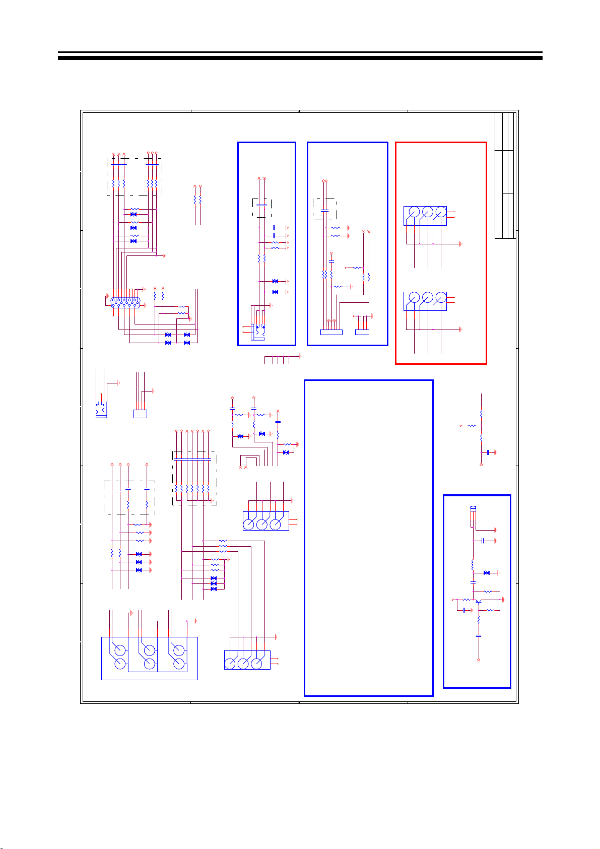
Date: Feb. 3,2010
RIN- 4
GIN- 4
RIN+ 4
GIN+ 4
BIN+ 4
BIN- 4
APPRD:
1
2
CN12
CN12
VGA IN
PH_L
PH_R
HP_DET
12345
3
4
5
CN4
CN4
YPbPr & AV IN
C496 47nFC496 47nF
C495 47nFC495 47nF
C486 47nFC486 47nF
R550 33RR550 33R
R548 33RR548 33R
R546 33RR546 33R
R145 75RR145 75R
E13 NCE13 NC
R144 75RR144 75R
E12 NCE12 NC
R143 75RR143 75R
E11 NCE11 NC
162738495
10
1617
1112131415
SIDE_CVBS
SIDE-AU-L
1122334
CN606
CN606
Head Phone
Head Phone
REAR_AV 4
LINE_IN_0R 4
LINE_IN_0L 4
REAR_AV
LINE_IN_0L
LINE_IN_0R
C26 47nFC26 47nF
C52 2.2uFC52 2.2uF
C54 2.2uFC54 2.2uF
R93 33RR93 33R
R95
75R
R95
75R
R111
R111
R77
R77
NC
E10NCE10
NC
R81 22KR81 22K
R82 22KR82 22K
E9NCE9
NC
E8NCE8
REAR_AUDIO_L
REAR_AUDIO_R
REAR_CVBS
HD_Pb
REAR_AUDIO_L
REAR_AUDIO_R
11229933884
L
L
Y
Y
D D
HD_Y
4
C485 47nFC485 47nF
R547 68RR547 68R
R-G-B-
SIDE-AU-R
4
VCOM0 4
VCOM0
C28 47nFC28 47nF
R94 68RR94 68R
12K
12K
12K
12K
VGA
VGA
CN513
CN513
R
R
C487 47nFC487 47nF
C497 47nFC497 47nF
R551 68RR551 68R
R549 68RR549 68R
VGA_HSYNC0 4
R146
100R
R146
100R
NC/Side_AV
NC/Side_AV
Pb
Pb
Closed to MST IC
VGA_VSYNC0 4
R147
100R
R147
100R
R148
10K
R148
10K
R149
10K
R149
10K
E4 NCE4 NC
E2 NCE2 NC
E1 NCE1 NC
E3NCE3
YPbPr_SOG 4
YPbPr_GIN+ 4
YPbPr_GIN- 4
YPbPr_GIN+
YPbPr_GIN-
YPbPr_SOG
C492 1nFC492 1nF
C488 47nFC488 47nF
C489 47nFC489 47nF
R541 68RR541 68R
R539 0RR539 0R
R540 33RR540 33R
Closed to MST IC
HD_Y
HD_Pr
REAR_CVBS
6
55776
V
V
Pr
Pr
UART-RX 4
R62 100RR62 100R
DDC_SCL_D DDC_SCL_D
DDC_SDA_D
NC
YPbPr_BIN+ 4
YPbPr_BIN+
YPbPr_BIN-
C501 47nFC501 47nF
C490 47nFC490 47nF
R542 33RR542 33R
R543 68RR543 68R
HD_Pb
UART-TX 4
DDC_SDA_D
YPbPr_BIN- 4
YPbPr_RIN+ 4
YPbPr_RIN+
C502 47nFC502 47nF
R544 33RR544 33R
HD_Pr
AV-JACK-1
AV-JACK-1
R58 100RR58 100R
YPbPr_RIN- 4
YPbPr_RIN-
C491 47nFC491 47nF
R545 68RR545 68R
E26 NCE26 NC
E25 NCE25 NC
E24 NCE24 NC
VGA Audio IN
LINE_IN_2R 4
C55 2.2uFC55 2.2uF
R105 22KR105 22K
E5NCE5
Closed to MST IC
R347NC R347NC
R346NC R346NC
R345NC R345NC
R9075R R9075R
R8875R R8875R
R13275R R13275R
SIDE_Y
14433
CN5NCCN5
LINE_IN_1L 4
LINE_IN_1R 4
LINE_IN_1R
LINE_IN_1L
C5182.2UF C5182.2UF
C5172.2UF C5172.2UF
Closed to MST IC
VGA_LIN
VGA_RIN
C69
C69
560pF
560pF
C70
C70
560pF
560pF
R213
12K
R213
12K
R214
12K
R214
12K
R211 22KR211 22K
R210 22KR210 22K
NC
E15NCE15
NC
E16NCE16
12345
6
7
8
CN11CN11
LINE_IN_2L 4
SIDE_Pb
C59 2.2uFC59 2.2uF
R104 22KR104 22K
E6NCE6
R108
12K
R108
12K
NC
HP_DET
PH_L
PH_R
SIDE_CVBS
366
2211443
SIDE_Pr
6
5
5
SIDE-AU-R
6
SIDE-AU-L
7
8
C27
C27
R112
R112
SIDE-AU-L
5
7
8
SIDE_AV
E7NCE7
SIDE_CVBS
5
NC
47nF
47nF
33R
33R
NC
SIDE-AU-R
R118
75R
R118
75R
7
7
8
8
R136
12K
R136
12K
NC
PH_L
PH_R
CN6NCCN6
221
C C
DVD INPUT
NC
AV Output
DVD_IN_R
C528 2.2UFC528 2.2UF
DVD-Rin
R68 100RR68 100R
DVD_AR
DVD_IN_R 4
DVD_IN_L 4
DVD_IN_L
DVD-Lin
R76 100RR76 100R
DVD_AL
1234567
J3
C533 2.2UFC533 2.2UF
Closed to MST IC
R70
12K
R70
12K
R63
12K
R63
12K
DVD_AV
47nF
47nF
C35
C35
+3.3V_SB
47R
47R
R69
R69
R67
75R
R67
75R
DVD_CVBS
+5V
J5
7pin 2.0mmJ37pin 2.0mm
R71NCR71
4
DVD POWER
B B
DVD_ON/OFF
NC
R74
150R
R74
150R
DVD_ON/OFF
IRIN
IRIN
R78
R78
123
J36
J36
112233445
SIDE_CVBS
22R
22R
J35
J35
112233445
CON4J5CON4
SIDE_Y
SIDE-AU-L
SIDE_Pb
NC/AV-JACK-3/AV
NC/AV-JACK-3/AV
8
8
7
7
6
5
6
SIDE-AU-R
8
8
7
7
6
5
6
NC/AV-JACK-3/YPbPr
NC/AV-JACK-3/YPbPr
+3.3V
R27
R27
C34
C34
For 32inch LED TV
HP_DET
R358
R358
R356
100K
R356
100K
R357
R357
PH_DETECT
G1S2S
J37
Single RCA
J37
Single RCA
3
SPDIFOUT
L2
L2
FB_11_OHM_500MA
FB_11_OHM_500MA
E14 NCE14 NC
1uF
1uF
C29
C29
150R
150R
1
0.1uF
0.1uF
R311KR31
C33
C33
SPDIF_OUT
SPDIF_OUT
100R
100R
100K
100K
C200
C200
C37
C37
33pF
33pF
R32
150R
R32
150R
3 2
Q7
3906Q73906
1K
0.1uF
0.1uF
SIDE_Pr
+5V
SPDIF Output
A A
1
CHECKED:
SHEET: 2 OF 9 VER:1.0
DESIGN:George Guo
MODEL: MSAV3207-K3
TITLE: YPBPR VGA AV IN/OUT
2
3
4.7uF
4.7uF
4
R29
220R
R29
220R
5
- 33 -
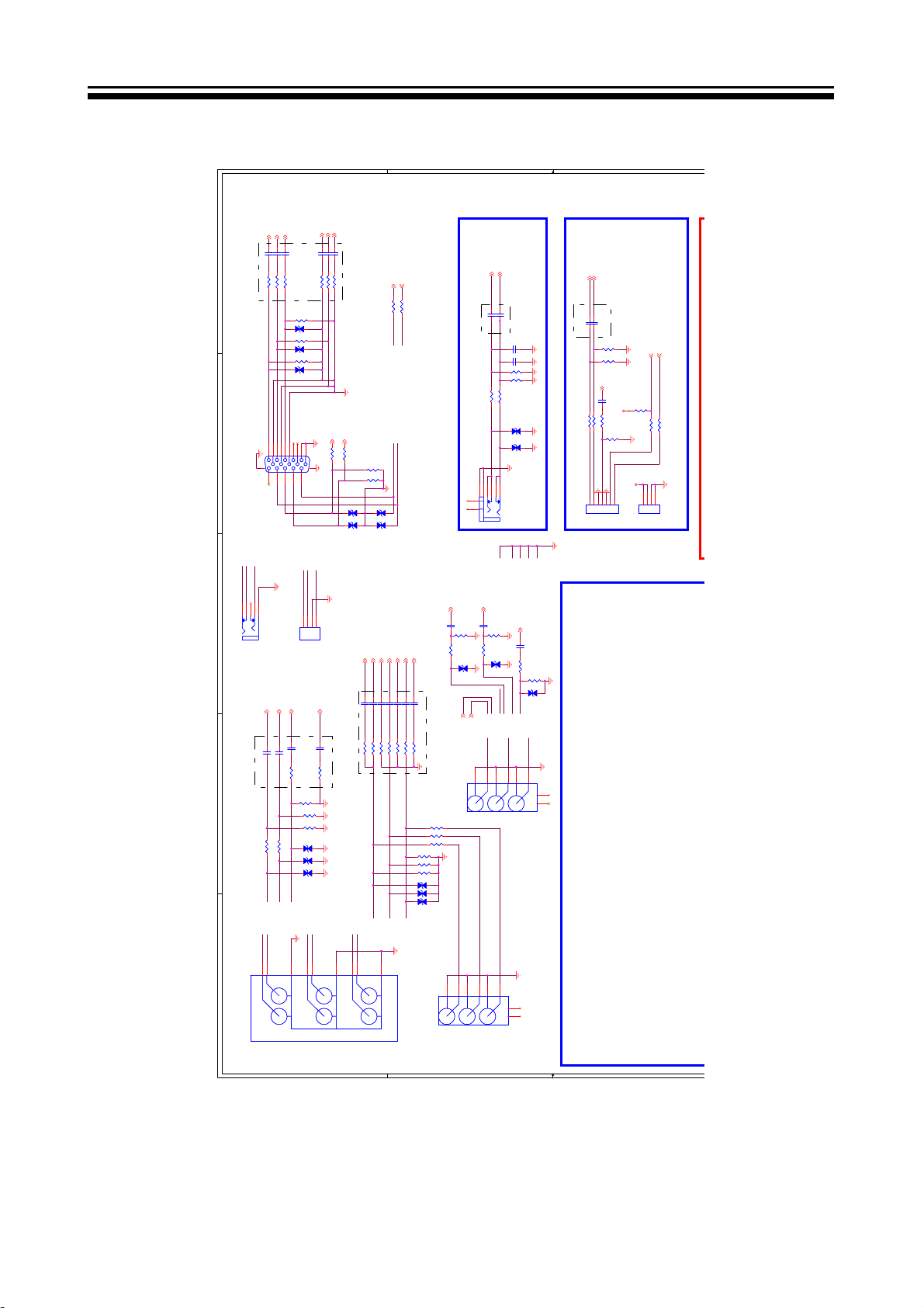
1617
CN12
CN12
VGA IN
PH_L
PH_R
HP_DET
12345
CN606
CN606
LINE_IN_0R
C52 2.2uFC52 2.2uF
R81 22KR81 22K
REAR_AUDIO_R
RIN+ 4
GIN+ 4
BIN+ 4
C496 47nFC496 47nF
C495 47nFC495 47nF
C486 47nFC486 47nF
R550 33RR550 33R
R548 33RR548 33R
R546 33RR546 33R
R145 75RR145 75R
E13 NCE13 NC
R144 75RR144 75R
E12 NCE12 NC
R143 75RR143 75R
E11 NCE11 NC
162738495
1112131415
Head Phone
Head Phone
LINE_IN_0R 4
LINE_IN_0L 4
LINE_IN_0L
C54 2.2uFC54 2.2uF
R82 22KR82 22K
REAR_AUDIO_L
REAR_AV 4
REAR_AV
C26 47nFC26 47nF
R93 33RR93 33R
E10NCE10
E9NCE9
E8NCE8
REAR_CVBS
10
SIDE_CVBS
SIDE-AU-L
1122334
R95
75R
R95
75R
R111
R111
R77
R77
NC
NC
NC
SIDE-AU-R
4
RIN- 4
GIN- 4
BIN- 4
C487 47nFC487 47nF
C497 47nFC497 47nF
C485 47nFC485 47nF
R551 68RR551 68R
R549 68RR549 68R
R547 68RR547 68R
Closed to MST IC
R-G-B-
VGA_HSYNC0 4
VGA_VSYNC0 4
R147
100R
R147
100R
R146
100R
R146
100R
VGA
VGA
E2 NCE2 NC
E1 NCE1 NC
CN513
NC/Side_AV
CN513
NC/Side_AV
VCOM0 4
VCOM0
C28 47nFC28 47nF
R94 68RR94 68R
Closed to MST IC
12K
12K
12K
12K
R148
R148
R149
R149
YPbPr_SOG 4
YPbPr_SOG
C492 1nFC492 1nF
R539 0RR539 0R
10K
10K
10K
10K
E4 NCE4 NC
E3NCE3
YPbPr_GIN+ 4
YPbPr_GIN+
YPbPr_GIN-
C488 47nFC488 47nF
C489 47nFC489 47nF
R541 68RR541 68R
R540 33RR540 33R
HD_Y
YPbPr_GIN- 4
UART-RX 4
R62 100RR62 100R
DDC_SCL_D DDC_SCL_D
DDC_SDA_D
NC
YPbPr_BIN+ 4
YPbPr_BIN+
YPbPr_BIN-
C501 47nFC501 47nF
C490 47nFC490 47nF
R542 33RR542 33R
R543 68RR543 68R
HD_Pb
UART-TX 4
DDC_SDA_D
YPbPr_BIN- 4
R58 100RR58 100R
YPbPr_RIN+ 4
YPbPr_RIN+
YPbPr_RIN-
C491 47nFC491 47nF
C502 47nFC502 47nF
R545 68RR545 68R
R544 33RR544 33R
E26 NCE26 NC
E25 NCE25 NC
E24 NCE24 NC
HD_Pr
YPbPr_RIN- 4
VGA Audio IN
LINE_IN_2R 4
C55 2.2uFC55 2.2uF
R105 22KR105 22K
E5NCE5
Closed to MST IC
R347NC R347NC
R346NC R346NC
R345NC R345NC
R9075R R9075R
R8875R R8875R
R13275R R13275R
LINE_IN_1L 4
LINE_IN_1R 4
LINE_IN_1R
LINE_IN_1L
C5182.2UF C5182.2UF
C5172.2UF C5172.2UF
Closed to MST IC
VGA_LIN
VGA_RIN
C69
C69
560pF
560pF
C70
C70
560pF
560pF
R213
12K
R213
12K
R214
12K
R214
12K
R211 22KR211 22K
R210 22KR210 22K
NC
E15NCE15
NC
E16NCE16
12345
6
7
8
CN11CN11
LINE_IN_2L 4
R136
12K
R136
12K
NC
PH_L
PH_R
CN6NCCN6
SIDE_AV
R108
12K
R108
12K
C59 2.2uFC59 2.2uF
47nF
47nF
C27
C27
NC
R104 22KR104 22K
33R
33R
E6NCE6
R112
R112
R118
75R
R118
75R
NC
E7NCE7
SIDE_CVBS
HP_DET
SIDE-AU-L
SIDE-AU-R
PH_L
PH_R
SIDE-AU-L
SIDE_CVBS
SIDE-AU-R
1
6
5
221
44336
5
7
7
8
8
DVD INPUT
NC
DVD_IN_R 4
DVD_IN_R
C528 2.2UFC528 2.2UF
DVD-Rin
R68 100RR68 100R
DVD_AR
DVD_IN_L 4
DVD_IN_L
DVD-Lin
R76 100RR76 100R
DVD_AL
1234567
J3
C533 2.2UFC533 2.2UF
Closed to MST IC
R70
12K
R70
12K
R63
12K
R63
12K
DVD_AV
47nF
47nF
C35
C35
+3.3V_SB
47R
47R
R69
R69
R67
75R
R67
75R
DVD_CVBS
+5V
J5
7pin 2.0mmJ37pin 2.0mm
R71NCR71
4
DVD POWER
DVD_ON/OFF
DVD_ON/OFF
NC
R74
150R
R74
150R
IRIN
IRIN
R78
22R
R78
22R
123
CON4J5CON4
5 4 3 2 1
CN4
CN4
YPbPr & AV IN
REAR_AUDIO_L
REAR_AUDIO_R
11229933884
L
L
Y
Y
SIDE_Pr
SIDE_Y
CN5NCCN5
SIDE_Pb
5
221144336
5
6
7
7
8
8
NC
HD_Pb
HD_Y
HD_Pr
REAR_CVBS
4
6
55776
V
R
V
R
AV-JACK-1
Pb
Pb
AV-JACK-1
Pr
Pr
AV Output
D D
C C
B B
- 34 -
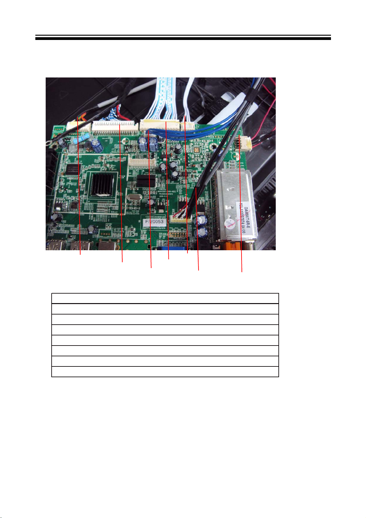
7-3 .Wiring Connection Diagram
4
NO.N ame
1
2
3
4
5
6
7
Connection Wire(For Speaker)
Connection Wire(Power For Mainboard)
LVDS Wire
Connection Wire(For Keyboard and Remote)
Connection Wire(For BackLight ON/OFF))
DVD POWER
Connection Wire(FOR DVD Mainboard)
3
6
2
5
7
1
- 35 -
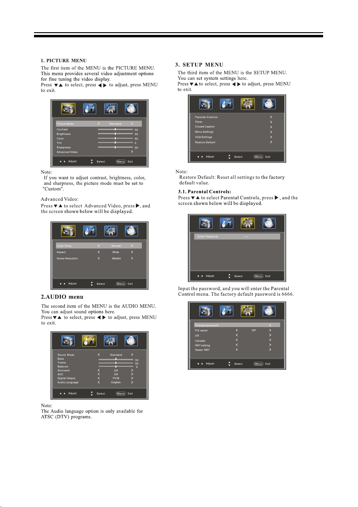
8. TV OPERATION
- 36 -

- 37 -
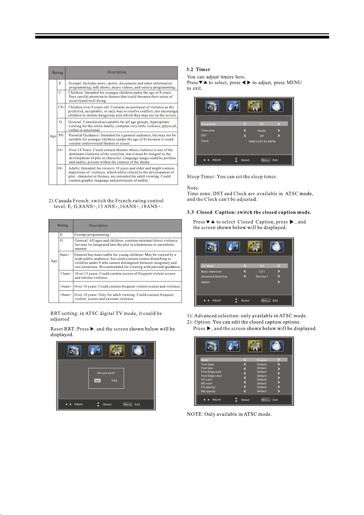
Press ENTER Key To Select
- 38 -
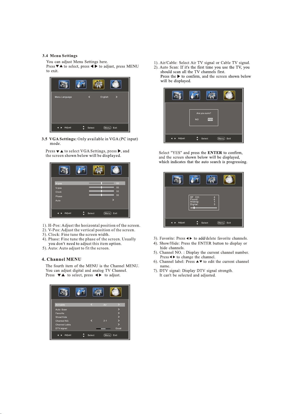
Press ENTER Key To Select
- 39 -
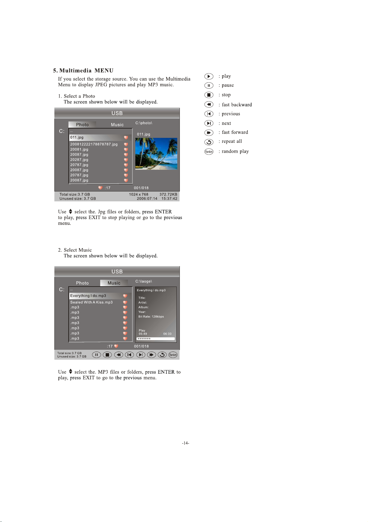
- 40 -

8.1 How to enter into the factory model
1. You can press "source-2-5-8-0" to go into factory setting. Presse the key "exit"
to shut the factory setting.
Content:
1: ADC setting: set ADC value of YUV,VGA. It can also be auto-set. Adopt 100%
color bar to yuv and Checkerboard signal to vga.
2:Color Temp.:
3:Video Quality:
4:Sound Quality:
5:Curve Setting:
6:Aging Mode:
7:Other Setting:
8:SW Upgrade:
9:Shipment:
7KH¿UVWOLQHLV6:9HU1R
- 41 -

8.2 How to update software
Haier MSD318QT F/W upgrade with USB SOP
Step 1: Ready for F/W Upgrade
1.1 Prepare a USB memory .
&RS\WKHVRIWZDUH¿OHPHUJHIURP\RXUFRPSXWHUWRWKH86%PHPRU\DQGUHPRYHLW
from computer’s USB port!
Step 2: F/W Upgrade
2.1 AC ON
2.2,Then input USB, press POWER.
2.3 Then press "source-2-5-8-0" and choose "SW Upgrade",and then press "ENTER".
2.4,Now you should choose "Yes" and then press "ENTER" TV begin to update.You should
remove the USB memory and reset TV after update.
Note: When Upgrade on the process, please don’t Power-Off!
- 42 -

9. Trouble shooting
9-1. Simple check
- 43-

9-2. Main board failure check
Service guide
1) Black creen
Is power LCD normal?
J15
2
2) White screen
11
6
J15
Check Q2,Q3 and the
2
5
on VCC pins of J9
Check if Q31 is working
Check if J9 is
Signal on J9
- 44 -

3) Panel display abnormally
connector J9 is at normal level
- 45-

4) No sound
No sound
Check the
input
source
Reset
volume
Check the
speakers
Check if the power supply
system is damaged, short
circuit or mis-connected
Check the volume control
circuit from U19
N
Y
N
Y
Y
Y
Check if there is sound input
signal
Y
Check if the volume control is
at 0 level or muted
N
Check if there is output at
J11
N
Check if there is +12V input at
PIN7
Check if PIN1 of U19 is low
of U19
Y
voltage
Check the volume input
circuit from to
U19
N
N
Check if there is signal input atPIN
& PIN12 of U16
Y
Replace U19
3
- 46-
5˅TV failure
TV no channel
Fix the RF
set
Check if there
is I2C signal
PIN7 of TUNER1
N
Check the I2C
circuit
between
U11 and
U24
at PIN6 &
N
Y
Check the
tuner
Check if there is RF
signal input
Y
Check if there is
+5V at PIN2 of
U24
Y
Check if there is
intermediate
frequency signal
output at PIN12 of
U24
N
Y
Check the signal
circuit between
U11 and U24
Check the power
supply circuit to
this PIN
- 47 -
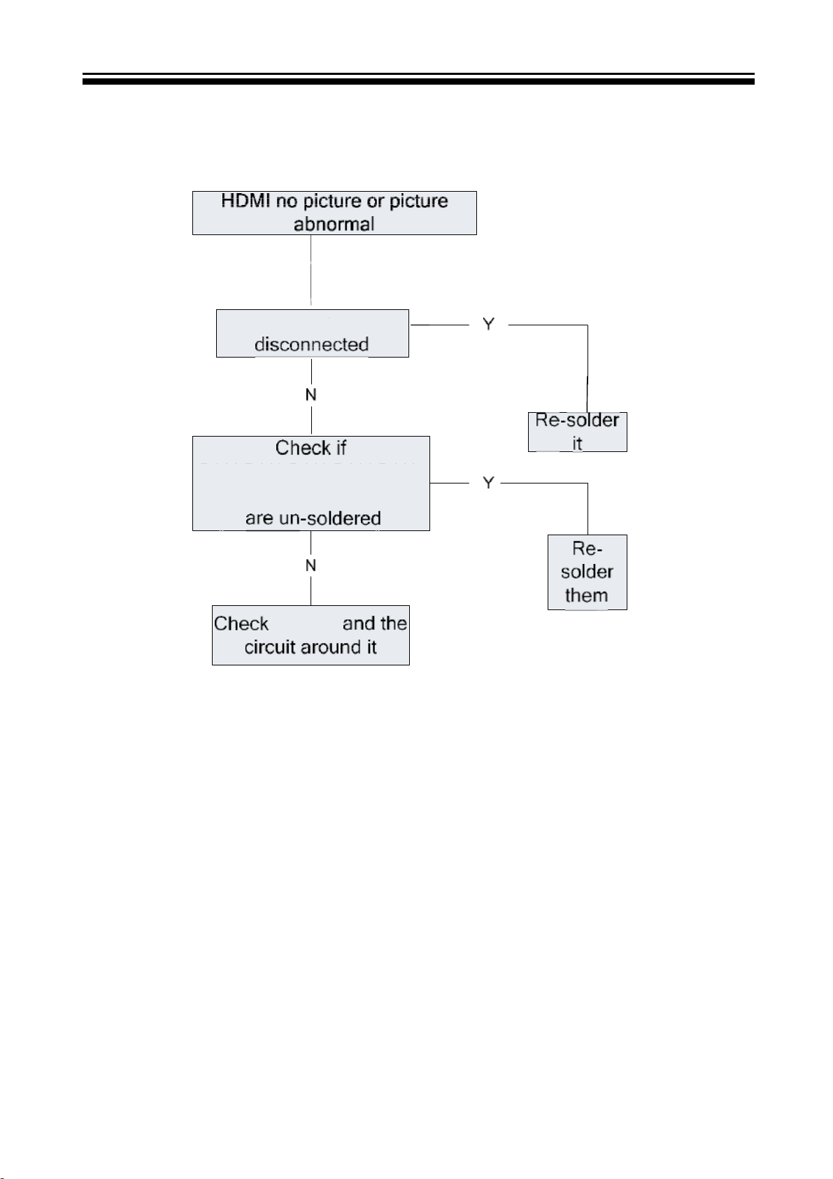
6) HDMI no picture or picture abnormal
If CN10 is
R301,R310,R319,R317,
R111,R112,R113,R114,R116,
R351,R338,R343
R117,R100,R105,R106,R108.
Q11,Q12
2
Q305
- 48 -
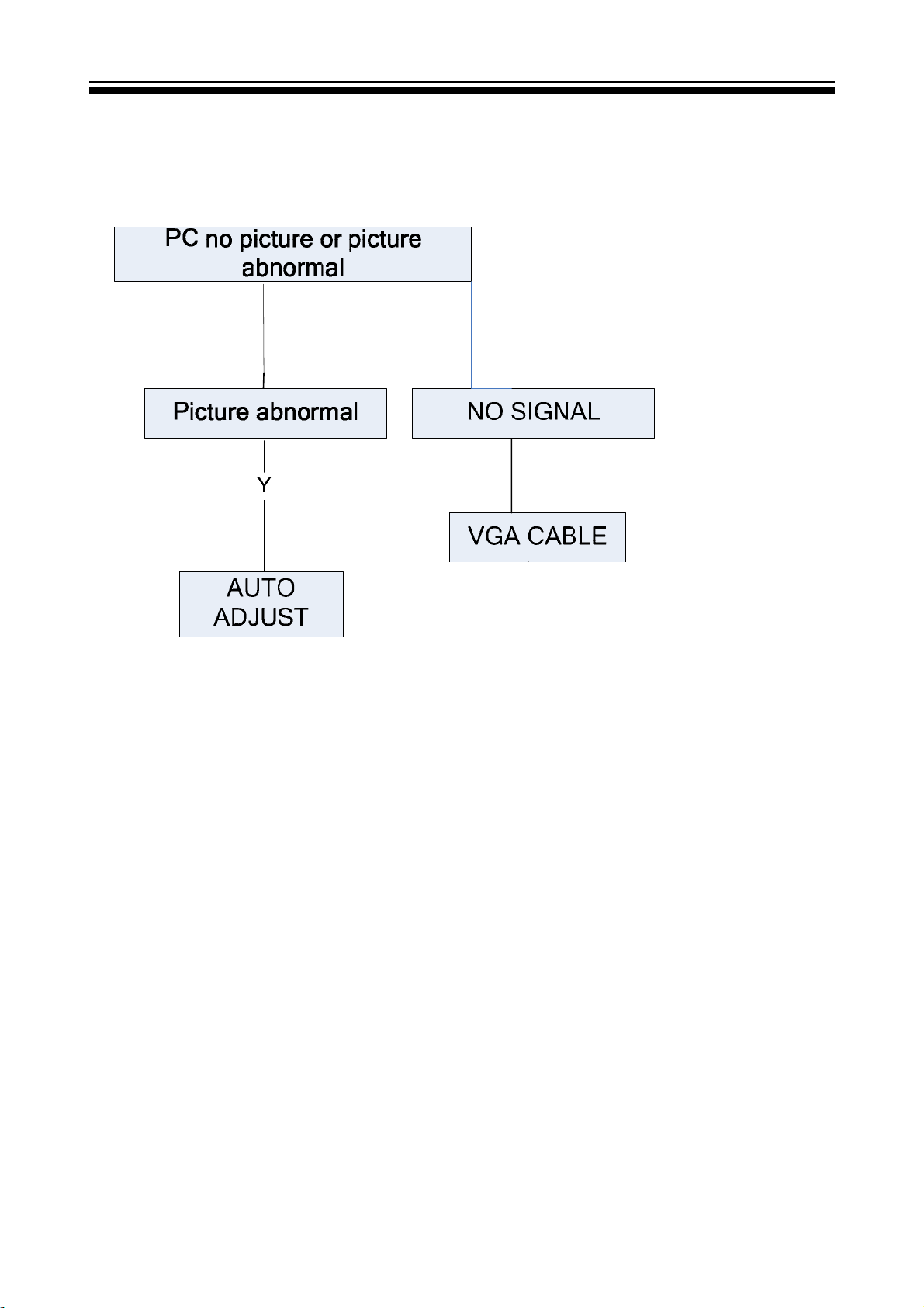
7) PC no picture or picture abnormal
- 49 -
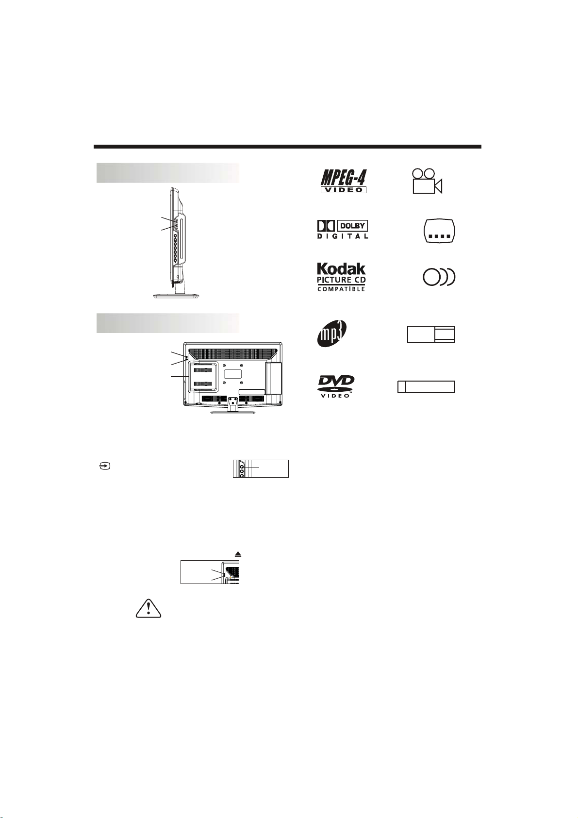
10.1 DVD OPENATION
DVD SIDE PANEL
(LEC19B1320)
MPEG4 files on discs
OPEN/CLOSE
PLAY/PAUSE
Disc with its content side
(shiny side) facing the front
of the unit, insert vertically
into the disc tray
Dolby Digital
DVD OPERATION
9
Multi-angle
32
Subtitle choices
8
DVD SIDE PANEL
(LEC22B1380 / LEC22B1380W / LEC24B1380)
OPEN/CLOSE
PLAY/PAUSE
Disc with its content side
(shiny side) facing the front
of the unit, insert vertically
into the disc tray
How to play a DVD disc
1. Change TV input source to "DVD" mode by pressing
button on remote or Source button
on the side of the TV.
2. Place DVD disc in player with the content side
(shiny side) facing the front of the unit.
3. DVD disc will automatically be loaded in to the player
and begin to play.
4. To eject the DVD disc, press Eject/Insert
button on remote or the button on the
side of the unit.
CH LIST/
OPEN/CLOSE
PLAY/PAUSE
SOURCE
Caution
KODAK picture CD
MP3 files on
CD-R/CD-RW
DVD video
Audio choices
16:9
TV Aspect
Ratio modes
RESTRICTED
R
Parental Lock
LB
This product incorporates copyright
protection technology that is protected
by method claims of certain
U.S.patents and other intellectual
property rights owned by Macro vision
Corporation and other rights owners.
Use of this copyright protection
technology must be authorized by
Macro vision Corporation, and is
intended for home and other limited
viewing uses only. Unless otherwise
authorized by Macro vision Corporation.
Reverse engineering or disassembly is
prohibited.
The product complies with the KODAK
Picture CD format and will display
KODAK Picture CDs. The "KODAK
Picture CD Compatible" logo is a
trademark of Eastman Kodak Company
and is used with permission.
This DVD Player has a Class 1 laser which may
be harmful to your eyes. Do not attempt to
disassemble the cabinet or make any adjustments.
Refer all servicing to a qualified professional.
Features
Disc formats supported by this player:
- 50 -
Manufactured under license from Dolby
Laboratories."Dolby" and the double-D
symbol are trademarks of Dolby
Laboratories. Confidential Unpublished
Works. 1992-1997 Dolby Laboratories, Inc.
All rights reserved.
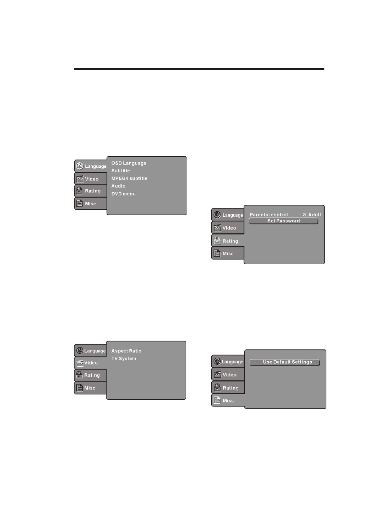
MENU OPERATION
Press the SETUP button on the remote control, the
SETUP MENU will be displayed. After accessing the
setup menu, press the direction buttons for up and
down movement to select an item desired, and press
RIGHT direction button to select the SUBMENU
item. Then press the ENTER/OK button to confirm.
Press LEFT direction button return to the menu of
upper level. To exit the setup, press the SETUP button
again. In the SETUP MENU, you may choose any of
the following options as you like.
LANGUAGE SETUP
Select Language in the setup menu, and display the
Language submenu:
DVD OPERATION
SYSTEM SETUP
Aspect Ratio
Select the aspect ratio.
Notes:
The image display ratio is related to the recorded disc
format. Some disc can not display images in the
aspect ratio you choose. If you play a disc recorded in
4:3 format on a wide screen TV, black bars will
appear on the left and right side of the screen. You
must adjust the screen setting depending on the type
of the television you have.
TV System
Select the different TV system.
Note: The DVD player setting should be matched to
your TV set.
refer to the instructions or your TV set.
RATING SETUP
Select Rating in the setup menu, and display
the Rating submenu:
For more information of output format,
OSD Language
Use this item to select the language for the
setup menu and screen display.
Subtitle
This option provides the preset subtitle language.
MPEG4 Subtitle(optional)
Select different MPEG4 subtitle encoding option.
Note: Not all players support this item.
Audio
Select the built-in disc dubbing language options.
DVD Menu
This option provides the film's menu language
options.
VIDEO SETUP
Select Video in the setup menu, and display the
Video submenu:
desired
Parental Control
Set the parental control feature of the player
Note: Password is needed before setting Parental
Control.
Set Password
Input four digits (password), then press ENTER
/Okto confirm.
Note: If you forget your password, please use the
universal password 6666 to unlock.
MISC SETUP
Select MISC in the setup menu, and display
the submenu:
- 51 -
Use Default Settings
Reset setup data to factory default value.

DVD OPERATION
MP3/WMA/JPEG PLAYBACK
The MP3/WMA disc has such a directory structure as
shown picture above.
Press Direction key to choose the root directory and
then press ENTER/OK button to enter into the sub
directory. Press Direction key to choose the desired
track and then press ENTER/OK or PLAY to enjoy
the music or movie. If you want to return to the upper
menu, press Direction key to choose the icon
and press ENTER/OK button.
Filter: Allows selecting the categories of files
displayed in the browser list.
Repeat: To switch different repeat playing mode
Mode: Select different playing mode as follows:
Normal: Shuffle mode is cancelled.
Shuffle: Shuffle mode enabled. When playback
reaches the end of the currentchapter/track, playback
jumps to a random chapter/track. As the end of each
chapter/track is reached, another random
chapter/track will be played until all tracks/chapters
have been played or the Shuffle mode is cancelled by
toggling to a different Mode Option.
Edit Mode: To enable programmed playback mode.
When you select the mode, press LEFT Direction
key to directory and press ENTER/OK to choose the
desired track and press Add to program and press
Program view and press the Edit mode to cancel the
edit mode. At last press Left key to display program
track and press ENTER/OK to start program
playback.
Program view: Display program track.
Brower view: Display track directory.
Add to program: Choice the track press Add to
program to add the track of the program play
directory.
Clear program: In the complete stop state(press the
STOP button twice), First press Edit mode to enable
the edit mode. Press Left key to program track and
press ENTER/OK to cancel the desired track. press
Clear program to delete the track of the program
play directory.
PICTURE CD PLAYBACK
The PICTURE CD disc has such a directory structure
structure as shown in the following picture.
Press Direction key to choose the root
directory and then press ENTER/OK button to
enter into the sub directory. Press Direction
key to choose the desired picture and then
press ENTER/OK or PLAY to enjoy the
picture. If you want to return to the upper menu,
press Direction key to choose the icon and
press ENTER/OK button.
Image rotation
In picture play state, press Direction key to
rotate the picture.
- 52 -

DVD OPERATION
Function Buttons
INSERT/EJECT
Eject the disc, press the INSERT/EJECT key;
Insert the disc, press the INSERT/EJECT
key again.
Insert a disc into the DVD player but could
not get it to work press the INSERT/EJECT
key on the remote or on the TV unit to eject
the disc. When a disc is ejecting or is ejected
but not take out, press the INSERT/EJECT
key on the remote or on the TV unit to insert
the disc.
SUBTITLE
Press the button to choose different
captions(Requires support from disc)
GOTO
For DVD discs, press the button to choose
the desired title and chapter andsearch the
desired title time and chapter time.For Super
VCD,VCD,CD discs, press this button to
search the desired disc time and track time
and choose the desired track.
Note: During VCD playback, the PBC mode
must be set to OFF.
0-9 keys
These keys are used to input the time, as well
as title, chapter and track numbers.When a
numeric item is displayed on the screen,
press the 0-9 keys to select the desired entry,
and press ENTER/OK to confirm.
When a VCD is playing(with PBC off), press
the 0-9 keys to select a track directly.
MENU
During DVD playback, press MENU to
display the disc menu of the current title.
During VCD/SVCD playback, press MENU
to control PBC ON/OFF.
SETUP
Press the button to enter the system setting
menu. Press the button again to exit the
menu.
RETURN
When DVD/SVCD/VCD displaying, press
RETURN button to the menu(PBC ON only).
DISPLAY
Press the button to show the information of
the current playing disc.
ENTER
Press the button to confirm your choice on
screen.
REV
During DVD, CD Mp3 or VCD playback,
press REV to scan in reverse.
The player will review the disc at different
times speed. Press PLAY/PAUSE to
resume normal playback.
FWD
During DVD, CD,MP3, or VCD playback,
press FWD to scan forward.The player
will cue the disc at different speed. Press
PLAY/PAUSE to resume normal playback.
PREV
During DVD, CD,MP3, or VCD playback,
press PREV to play the previous chapter,
title or track.
NEXT
During DVD,CD,MP3, or VCD playback,
press NEXT toplay the next chapter, title
or track.
STOP
Press the button once and the player will be
in memory stop state. Continuously press
this button twice and the player will be in
complete stop state.
Play/Pause
In pause state or stop state, press the button,
the player will be in playing state.In play
state, press the button the player will be in
pause state.
REPEAT
Press to select between different
repeat modes Repeat Chapter / Repeat
Title / Repeat Off for DVD discs ,
Repeat Single/ Repeat Folder/All/ Repeat
Off(for VCD/CD/MP3 discs)
AUDIO
Changes the audio language or audio
channel.
- 53 -

DVD TROUBLE SHOOTING
If you have any questions, please consult the troubleshooting guide below:
NO PICTURE OR SOUND
Ensure the power button is on.
Ensure the power outlet is operational.
Ensure the power cord is not damaged.
Ensure the power plug is connected
firmly to the outlet.
PICTURE BUT NO SOUND
Ensure the audio is not set to mute.
Ensure you have set the player s AUDIO
settings correctly.
POOR PICTURE OR SOUND
Ensure you have set the player s AUDIO
settings correctly
Ensure the disc is not scratched or stained.
BAD DISC DISPLAYED
Ensure the disc is not warped, damaged or
deformed.
REMOTE NOT WORKING
Make sure the Main unit s POWER button is on
Ensure the remote batteries are working.
Point the remote control directly at the player s
IRsensor.
Remove any obstacles between the remote and
theIR sensor.
UNIT NOT WORKING
Turn off the power, and then turn it on again.
NO DISC DISPLAYED
Ensure you have put the disc on the tray.
Ensure the disc is not upside down.
Ensure the disc is not distorted, stained or
scratched.
Ensure the disc is not badly stained or
damaged.
Ensure the disc format is compatible with
the player.
Please check whether you have tried to play a
software CD. If so, please restart the player.
- 54 -
11.1 PANNEL FAILURE
Failure Mode
Part Name Description Phenomena Failure cause
White Screen B/L normal,
only white screen
display
Maybe caused
Black Screen B/L normal,
only Black screen
display
FIIcker Crosstalk
Circuit
by surge current
and EDS
LCD
Vcom imbalance
Abnormal Color Only
color abormal
Only
Abnormal Color
color abnormal
Capacitance
improper bring
crosstalk inside
LCD pannel
1.Chip
lose action
2.IC short or
jointion bad
3.Pannel and vsc
connect bad
- 55 -

Part Name Description Phenomena Failure cause
Incoming Inspection
Standard
Bladder between Polarizer
and top glass
Tine or rigidity arose
Eyewinker inside Polarizer
Panel or
Polarlzer
Dot Defect
Polarizer Bubble Bladder in Polarizer
Polarizer Scratch Polarizer Scratch
Bright dot dark dot in
pannel
Circuit
F/M inside
Polarizer
Abnormal Display Abnormal Display
Flashing
Eyewinker inside
Polarizer
Bright and dark
display alternately
1.Chip lose action
2.IC ahort or jointiog bad
3.Pannel and vsc connect
bad
- 56 -

9-3. Pannel failure
Failure Mode
Part Name Description Phenomena Failure cause
Block Defect :TCP cracking or cracking
Dim or L/D :TCP Sunken
:TCP lead cracking
:ACF bonding short
:Awful environment and
something electric enter
into LCD
:Mis-align between TCP and
Panel
:Panel failure
:TCP failure
TCP
V B/D Vertical bar
V Dim Vertal gray line
Vertical color
V L/D
H B/D Horizontal bar
line(light or dark
forever)
H Dim
H L/D
Horizontal gary
line
Horizontal
line(light or dark
forever)
- 57 -

Failure Mode
Part Name Description Phenomena Failure cause
Mechanlcal
Nolse
Ripple Connectric circle
When
turn panel,appear
cacophony
Caused
by Mechanica
noise of backlight
unit
Causeed by
between
mechanism and
pannel
B/L off B/L lose action
B/L dark B / L brightness
darker than
normal
B/L
wire damaged
B/L wire open Without backlight Operation
B/L shut down B/L shutdown in
F/M F/M
B/L
wire damaged
sometime
inB/L ,white,balck
Rotundity
or wirelike
*Connect
badness
between wire and
electrode
*Connect
badnessShort
between wire and
electrode
Operation
abnormal
or systemic noise
abnormal
or systemic noise
Short bitween
lamp housing and
wire, Because
consume power
too much
F/M in B/L unit
- 58 -

Failure Mode
Part Name Description Phenomena Failure cause
Light leakage
Brightness
at bottom of LCM
brighter
than normal
B/L unit badness
Mechanlcal or B/
L
Uniformity
Mount hole
B/L brightness
asymmetric
Lack screw
or screw damage
Sheet in B/L unit
is uneven
*Lack screw
Screw damage
- 59 -

Sincere Forever
Haier Group
Haier Industrial Park, No.1, Haier Road
266101, Qingdao, China
http://www.haier.com
Printed in China
 Loading...