

Page 1
SERVICE MANUAL
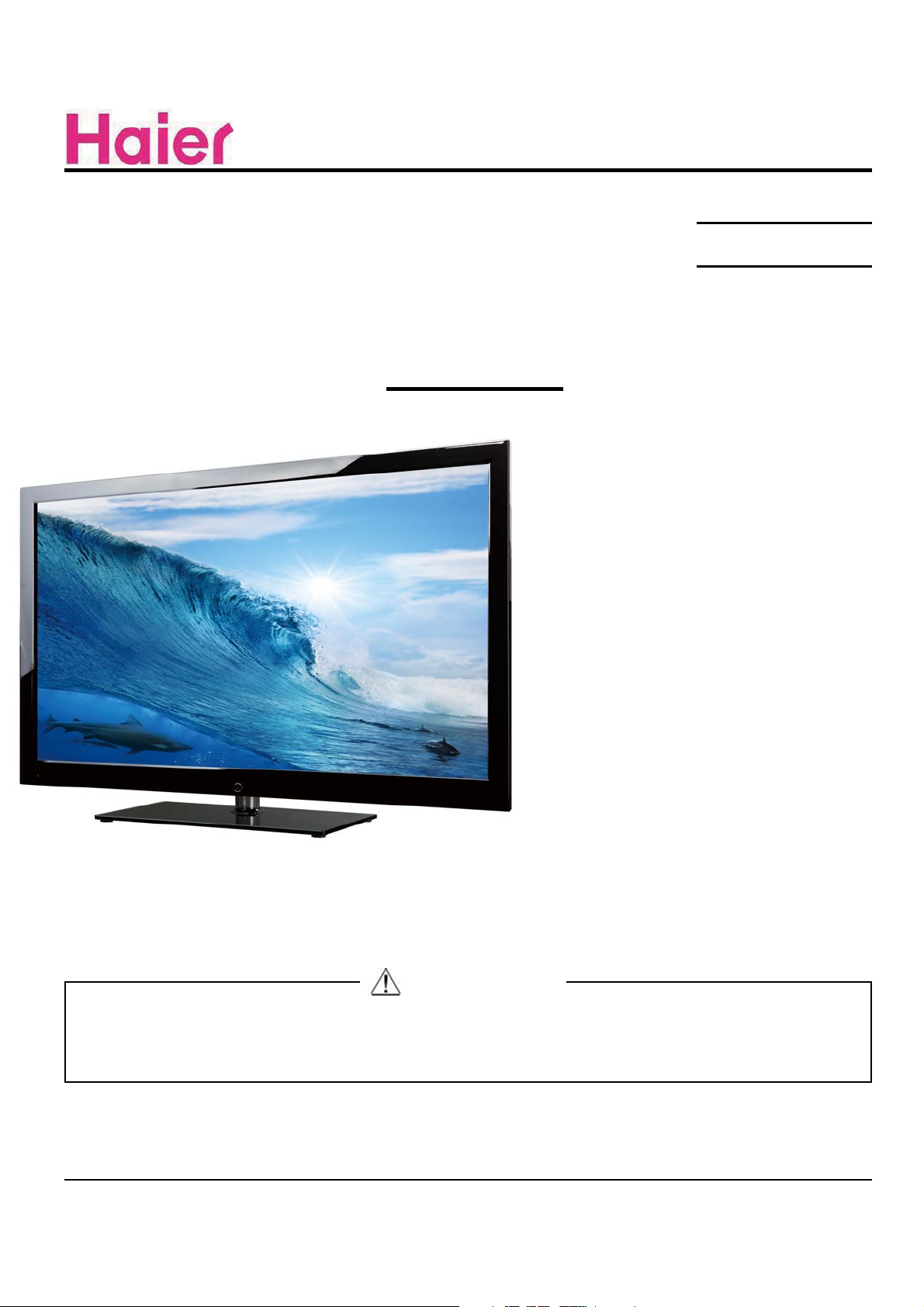
LED TV
Model No. LE55B1381a
MST 318
Chassis
WARNING
This service information is designed for experienced repair technicians only and is not designed for use by the general public.
It does not contain warnings or cautions to advise non-technical individuals of potential dangers in attempting to service a product.
Products powered by electricity should be serviced or repaired only by experienced professional technicians. Any attempt to service or repair
the product or products dealt with in this service information by anyone else could result in serious injury or death.
©2011 Qingdao Haier Electronics Co., Ltd.
All rights reserved. Unauthorized copying and distribution is a violation of law.
Haier Group
Page 2

Service Manual
Model No.:
Chapter 1: General Information
1-1. Table of Contents
1. General Information...........................................................................
1-1. Table of Contents
1-2. General Guidelines
1-3. Important Notice
1-4. How to Read this Service Manual
....................................................................................
3. Location of Controls and Components...........................................
3-1. Board Location
3-2. Main Board
3-3. Power Board
3-4. LCD Panel
4. Disassemble and Assemble..........................................................
5. Installation Instructions..…....………………...........………….........
1
4
4
4
7
7
88
8
8
11
12
15
20
21
12snoitcennoCtnempiuqElanretxE1-5
42snoitcennoCIMDH2-5
6. Operation Instructions....…....………………...........………….........
6-1 Front Panel Controls
6-2 Back Panel Controls
6-3 Universal Remote Control
7. Electrical Parts…....………………...........………….........................
7-1. Block Diagram
7-2. Circuit Diagram
8. TV OPERATION........………….........................................................
8-1 TV OSD Menu
8-2 Upgrade software
8-3 Factory menu
27
27
27
28
29
29
30
39
39
45
46
- 01 -
Page 3

Service Manual
Model No.:
9. Trouble-shooting…………..............................................................
9-2. Main Board Failure Check
9-3. Panel Failure
51
15kcehCelpmiS.1-9
52
55
- 02 -
Page 4

Service Manual
Model No.:
1-2. General Guidelines
When servicing, observe the original lead dress. If a short circuit is found, replace all parts
which have been overheated or damaged by the short circuit.
After servicing, see to it that all the protective devices such as insulation barriers, insulation
papers shields are properly installed.
After servicing, make the following leakage current checks to prevent the customer from
being exposed to shock hazards.
1) Leakage Current Cold Check
2) Leakage Current Hot Check
3) Prevention of Electro Static Discharge (ESD) to Electrostatically Sensitive
1-3. Important Notice
1-3-1. Follow the regulations and warnings
Most important thing is to list up the potential hazard or risk for the service personnel to
open the units and disassemble the units. For example, we need to describe properly
how to avoid the possibility to get electrical shock from the live power supply or charged
electrical parts (even the power is off).
This symbol indicates that high voltage is present inside.It is dangerous to
make any king of contact with any inside part of this product.
This symbol indicates that there are important operating and maintenance
instructions in the literture accompanying the appliance.
1-3-2. Be careful to the electrical shock
7RSUHYHQW GDPDJHZKLFKPLJKWUHVXOWLQHOHFWULFVKRFN RU¿UH GRQRWH[SRVHWKLV79 VHW
to rain or excessive moisture. This TV must not be exposed to dripping or splashing water,
DQGREMHFWV¿OOHGZLWKOLTXLGVXFKDVYDVHVPXVWQRWEHSODFHGRQWRSRIRUDERYHWKH79
1-3-3. Electro static discharge (ESD)
Some semiconductor (solid state) devices can be damaged easily by static electricity. Such
components commonly are called Electrostatically Sensitive (ES) Devices. The following
techniques should be used to help reduce the incidence of component damage caused by
electros static discharge (ESD).
1-3-4. About lead free solder (PbF)
This product is manufactured using lead-free solder as a part of a movement within the
consumer products industry at large to be environmentally responsible. Lead-free solder
must be used in the servicing and repairing of this product.
8VHWKHJHQHZLQJSDUWVVSHFL¿HGSDUWV
Special parts which have purposes of fire retardant (resistors), high-quality sound
(capacitors), low noise (resistors), etc. are used.
When replacing any of components, be sure to use only manufacture's specified parts
shown in the parts list.
Safety Component
Ɣ&RPSRQHQWVLGHQWL¿HGE\PDUNKDYHVSHFLDOFKDUDFWHULVWLFVLPSRUWDQWIRUVDIHW\
- 03 -
Page 5

Service Manual
Model No.:
1-3-6 Safety Check after Repairment
&RQ¿UPWKDWWKH VFUHZVSDUWVDQGZLULQJZKLFKZHUHUHPRYHGLQ RUGHUWRVHUYLFHDUHSXW
in the original positions, or whether there are the positions which are deteriorated around
the serviced places serviced or not. Check the insulation between the antenna terminal or
external metal and the AC cord plug blades. And be sure the safety of that.
General Servicing Precautions
1. Always unplug the receiver AC power cord from the AC power source before;
a. Removing or reinstalling any component, circuit board module or any other receiver
assembly.
b. Disconnecting or reconnecting any receiver electrical plug or other electrical
connection.
c. Connecting a test substitute in parallel with an electrolytic capacitor in the receiver.
CAUTION: A wrong part substitution or incorrect polarity installation of electrolytic
capacitors may result in an explosion hazard.
2. Test high voltage only by measuring it with an appropriate high voltage meter or other
voltage measuring device (DVM, FETVOM, etc) equipped with a suitable high voltage
probe.
Do not test high voltage by "drawing an arc".
3. Do not spray chemicals on or near this receiver or any of its assemblies.
4. Unless specified otherwise in this service manual, clean electrical contacts only by
applying the following mixture to the contacts with a pipe cleaner, cotton-tipped stick or
comparable non-abrasive applicator; 10% (by volume) Acetone and 90% (by volume)
isopropyl alcohol (90%-99% strength).
CAUTION:7KLVLVDÀDPPDEOHPL[WXUH
8QOHVVVSHFL¿HGRWKHUZLVHLQWKLVVHUYLFHPDQXDOOXEULFDWLRQRIFRQWDFWVLVQRWUHTXLUHG
Capacitors may result in an explosion hazard.
5. Do not defeat any plug/socket B+ voltage interlocks with which receivers covered by this
service manual might be equipped.
6. Do not apply AC power to this instrument and/or any of its electrical assemblies unless
all solid-state device heat sinks are correctly installed.
7. Always connect the test receiver ground lead to the receiver chassis ground before
connecting the test receiver positive lead.
Always remove the test receiver ground lead last. Capacitors may result in an explosion
hazard.
8VHZLWKWKLVUHFHLYHURQO\WKHWHVW¿[WXUHVVSHFL¿HGLQWKLVVHUYLFHPDQXDO
CAUTION: 'RQRWFRQQHFWWKHWHVW¿[WXUHJURXQGVWUDSWRDQ\KHDWVLQNLQWKLVUHFeiver.
9. Remove the antenna terminal on TV and turn on the TV.
10. Insulation resistance between the cord plug terminals and the eternal exposure metal
should be more than Mohm by using the 500V insulation resistance meter.
11. If the insulation resistance is less than M ohm, the inspection repair should be required.
If you have not the 500V insulation resistance meter, use a Tester. External exposure
metal: Antenna terminal Headphone jack
- 04 -
Page 6

Service Manual
Model No.:
Electrostatically Sensitive (ES) Devices
Some semiconductor (solid-state) devices can be damaged easily by static electricity.
Such components commonly are called Electrostatically Sensitive (ES) Devices.
Examples of typical ES devices are integrated circuits and some field-effect transistors
and semiconductor "chip" components. The following techniques should be used to help
reduce the ncidence of component damage caused by static by static electricity.
1. Immediately before handling any semiconductor component or semiconductorequipped assembly, drain off any electrostatic charge on your body by touching a known
earth ground. Alternatively, obtain and wear a commercially available discharging wrist
strap device, which should be removed to prevent potential shock reasons prior to applying
power to the unit under test.
2. After removing an electrical assembly equipped with ES devices, place the assembly
on a conductive surface such as aluminum foil, to prevent electrostatic charge buildup or
exposure of the assembly.
3. Use only a grounded-tip soldering iron to solder or unsolder ES devices.
4. Use only an anti-static type solder removal device. Some solder removal devices not
FODVVL¿HGDVDQWLVWDWLFFDQJHQHUDWHHOHFWULFDOFKDUJHVVXI¿FLHQWWRGDPDJH(6GHYLFHV
'RQRWXVHIUHRQSURSHOOHGFKHPLFDOV7KHVHFDQJHQHUDWHHOHFWULFDOFKDUJHVVXI¿FLHQW
to damage ES devices.
6. Do not remove a replacement ES device from its protective package until immediately
before you are ready to install it.
(Most replacement ES devices are packaged with leads electrically shorted together by
conductive foam, aluminum foil or comparable conductive material).
7. Immediately before removing the protective material from the leads of a replacement
ES device, touch the protective material to the chassis or circuit assembly into which the
device will be installed.
CAUTION: Be sure no power is applied to the chassis or circuit, and observe all other
safety precautions.
8. Minimize bodily motions when handling unpackaged replacement ES devices.
(Otherwise harmless motion such as the brushing together of your clothes fabric or the
OLIWLQJRI\RXUIRRWIURPDFDUSHWHGÀRRUFDQJHQHUDWHVWDWLFHOHFWULFLW\VXI¿FLHQWWRGDPDJH
an ES device.)
1-3-7. Ordering Spare Parts
Please include the following informations when you order parts. (Particularly the Version
letter)
1. Model number, Serial number and Software Version
The model number and Serial number can be found on the back of each product and the
Software Version can be found at the Spare Parts List.
2. Spare Part No. and Description
<RXFDQ¿QGWKHPLQWKH6SDUH3DUWV/LVW
- 05 -
Page 7

1-3-8. Photo used in this manual
The illustration and photos used in this Manual may not base on the final design of
products, which may differ from your products in some way.
1-4. How to Read this Service Manual
Using Icons:
,FRQVDUHXVHGWRDWWUDFWWKHDWWHQWLRQRIWKHUHDGHUWRVSHFL¿FLQIRUPDWLRQ7KHPHDQLQJRI
each icon is described in the table below:
Note:
A “note” provides information that is not indispensable, but may nevertheless be valuable
to the reader, such as tips and tricks.
Service Manual
Model No.:
Caution:
A “caution” is used when there is danger that the reader, through incorrect manipulation,
may damage equipment, loose data, get an unexpected result or has to restart(part of) a
procedure.
Warning:
A “warning” is used when there is danger of personal injury.
Reference:
A “reference” guides the reader to other places in this binder or in this manual, where he/
VKHZLOO¿QGDGGLWLRQDOLQIRUPDWLRQRQDVSHFL¿FWRSLF
- 06 -
Page 8
Service Manual
Model No.:
Model
Screen Size 54.6inch
Aspect Ratio 16:9
Resolution 1920x1080
Response Time (ms)
Angel ofView 176
Color Display16777216
No. of Preset Channels 203
OSD LanguageEnglish/France/Spaish
Color System NTSC
Audio System M/N
Audio Output Power
(Built-in) (W)
Audio Output Power
(outer) (W)
LE55B1381a
6 (GRAYTO
GRAY)
o
10W×2
No
Tot al Power Input (W) 160W
Voltage Range (V) AC100V-240V
Power Frequency (Hz) 50~60Hz
Net Weight (KG) 29
Gross Weight (KG) 34.2
Net Dim
Packaged Dimension
(MM)
ension (MM)
1302*325*855
1400*160*890
- 07 -
Page 9
3. Location of Controls and Components
3-1 Board Location
Service Manual
Model No.:
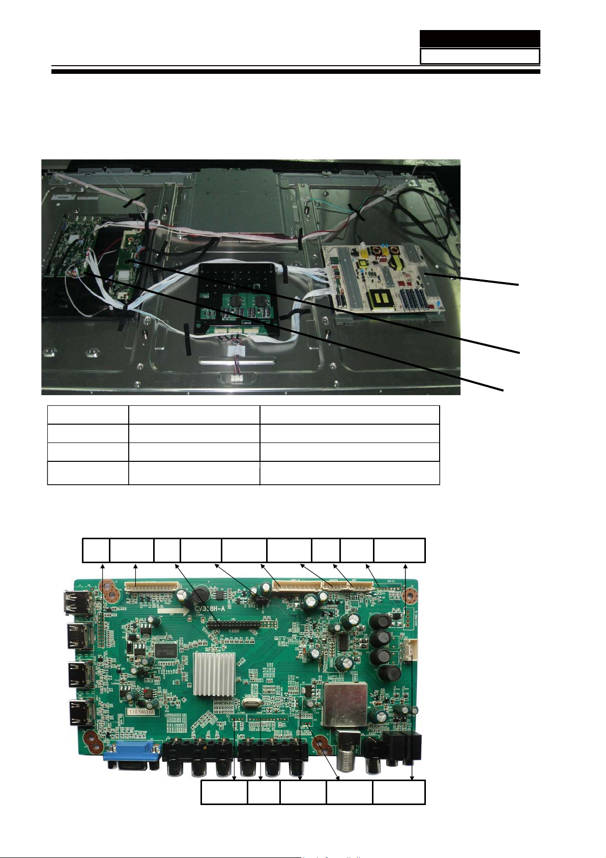
%%RDUG
No. Part Number Description
A Board
B Board
C Board
0113070686
0113050420
0113060163
Main board
Power board
120HZ control board
3-2 Main Board
J10:
HDMI
J4:IR&KEY
BOARD
J9:
LVDS
J6:PANEL
POWER
J5:POWER
IN
J1:
INVERTER
J2:
HDCP
J3:DVD
CTL
&%RDUG
$%RDUG
J8:AUDIO
POWER IN
J17:
S_VIDEO
J18:
YPBPR
J14:AUDIO
OUT
- 08 -
J19:AUDIO
IN
J12:
SPEAKER
Page 10
Service Manual
Model No.:
3-2-1 Function Description:
Main Board
Process signal which incept from exterior equipment then translate into signalthatpanel
can display.
Main board connector
Power connectors (J1, J5)
J1
Notes:
J1-Pin 4: Backlight on/off:
The system can turn on or turn off the backlight of TFT LED Panel throughthepower
supply unit path.
J5-Pin 9: System power on / standby
System board will use this pin to control system power.
J1-Pin 3: Control the luminance of backlight
The system can generate the PWN signal to control the strength of TFT LED Panel’s
backlight through this connector
J5
- 09 -
Page 11

Keypad and remote connector (J4)
Service Manual
Model No.:
Pin number
1
2
3
4
5
6
7
8
9
10
11
12
13
14
Signal name
GND
K7
K6
K5
K4
K3
K2
K1
K0
GND
IR
LED_G
LED_R
GND
Description
Ground
Power key
NC
CH- key
CH+ key
Vol- key
Vol+ key
Meny key
TV/AV key
Ground
IR Receive
Green Indicator
Red Indicator
+5V DC Power Supply
- 10 -
Page 12

Service Manual
Model No.:
Speaker connector J12
Pin number Signal nam e Description
1
2
3
4
R+
R-
L-
L+
Audio Right+channel Output
Audio Right- channel Output
Audio Left- channel Output
Audio Left+channel Output
3-3. Power Board
Pin-CON1 Connection And Function
NO. Pin Connection Function
1 AC-N AC INPUT NUTURE
2 AC-L AC INPUT LINE
Pin-CON2 Connection And Function TYPE:2.54MM*13PIN
NO. Pin Connection Function
1 12V 12V DC OUTPUT
2 12V 12V DC OUTPUT
3 GND 12V DC RETURN
4 GND 5V DC RETURN
5 GND 5V DC RETURN
65V 5VDCOUTPUT
75V 5VDCOUTPUT
85VSB 5VDCOUTPUT
9 PS-ON SMPS ON/OFF CONTROL(ON=HIGH)
10 5V 5V DC OUTPUT
11 5V 5V DC OUTPUT
12 GND 5V DC RETURN
13 GND 5V DC RETURN
Pin-CON3 Connection And Function TYPE:2.54MM*4PIN
NO. Pin Connection Function
1 GND 24V DC RETURN
2 GND 24V DC RETURN
3 24V 24V DC OUTPUT
4 24V 24V DC OUTPUT
Pin-CON4 Connection And Function TYPE:2.54MM*8PIN
NO. Pin Connection Function
1 GND 24V DC RETURN
2 GND 24V DC RETURN
3 GND 24V DC RETURN
4 GND 24V DC RETURN
5 24V 24V DC OUTPUT
6 24V 24V DC OUTPUT
7 24V 24V DC OUTPUT
8 24V 24V DC OUTPUT
- 11 -
Page 13

3-4. LED Panel
Service Manual
Model No.:
V546H1-LE5
- 12 -
Page 14

Service Manual
Model No.:
3-5 Interface Connec tions
CNF2 Connector Pin Assignment(187059-51221(P-two) or equivalent)
-
Symbol
No
GND
1
2
NC
NC
3
NC
4
NC
5
NC
6
SELLVDS
7
NC
8
NC
9
NC
10
GND
11
CH1[0]-
12
CH1[0]+
13
CH1[1]-
14
CH1[1]+
15
CH1[2]-
16
CH1[2]+
17
GND
18
CH1CLK-
19
CH1CLK+
20
GND
21
CH1[3]-
22
CH1[3]+
23
CH1[4]-
24
CH1[4]+
25
NC
26
Description
Ground
1
1
1
1
1
LVDS Data Format Selection 2
1
1
1
Ground
First pixel Odd LVDS Signal-
First pixel Odd LVDS Signal+
First pixel Odd LVDS Signal-
First pixel Odd LVDS Signal+
First pixel Odd LVDS Signal-
First pixel Odd LVDS Signal+
Ground
First pixel Odd LVDS Clock-
First pixel Odd LVDS Clock+
Ground
First pixel Odd LVDS Signal-
First pixel Odd LVDS Signal+
First pixel Odd LVDS Signal-
First pixel Odd LVDS Sig
nal+
1
No
Symbol
NC
27
CH2[0]-
28
29
CH2[0]+
CH2[1]-
30
31
CH2[1]+
CH2[2]-
32
CH2[2]+
33
GND
34
CH2CLK-
35
36
CH2CLK+
37
GND
38
CH2[3]-
39
CH2[3]+
CH2[4]-
40
41
CH2[4]+
42
NC
NC
43
GND
44
GND
45
GND
46
NC
47
48
59
50
51
-
-
VCC
VCC
VCC
VCC
Descrip tion
Second pixel Odd LVDS Signal-
Second pixel Odd LVDS Signal+
Second pixel Odd LVDS Signal-
Second pixel Odd LVDS Signal+
Second pixel Odd LVDS Signal-
Second pixel Odd LVDS Signal+
Ground
Second pixel Odd LV
Second pixel Odd LVDS Clock+
Ground
Second pixel Odd LVDS Signal-
Second pixel Odd LVDS Signal+
Second pixel Odd LVDS Signal-
Second pixel Odd LVDS Signal+
DC power supply
DC power supply
DC power supply
DC power supply
DS Clock-
N o t e :1)Reserved for internal use.Please leave it open
N o t e : 2)High=connect to +3.3V:JEIDA Format;Low=connect to GND or Open:VESA
Format
1
1
1
1
- 13 -
Page 15

Service Manual
Model No.:
CNF3 Connector Pin Assignment(187059-51221(P-two) or equivalent)
-
Symbol
No
GND
1
2
NC
NC
3
NC
4
NC
5
NC
6
NC
7
NC
8
GND
9
CH3[0]-
10
CH3[0]+
11
CH3[1]-
12
CH3[1]+
13
CH3[2]-
14
CH3[2]+
15
GND
16
CH3CLK-
17
CH3CLK+
18
GND
19
CH3[3]-
20
CH3[3]+
21
Description
Ground
1
1
1
1
1
1
1
Ground
Third pixel Odd LVDS Signal-
Third pixel Odd LVDS Signal+
Third pixel Odd LVDS Signal-
Third pixel Odd LVDS Signal+
Third pixel Odd LVDS Signal-
Third pixel Odd LVDS Signal+
Ground
Third pixel Odd LVDS Clock-
Third pixel Odd LVDS Clock+
Ground
Third pixel Odd LVDS Signal-
Third pixel Odd LVDS Signal+
No
Symbol
CH3[4]-
22
23
CH3[4]+
24
25
CH4[0]-
26
27
CH4[0]+
CH4[1]-
28
29
CH4[1]+
30
CH4[2]-
31
CH4[2]+
32
CH4CLK-
33
34
CH4CLK+
35
36
37
CH4[4]-
38
39
CH4[4]+
NC
40
41
NC
42
NC
NC
GND
GND
CH4[3]-
CH4[3]+
Descrip tion
Third pixel Odd LVDS Signal-
Third pixel Odd LVDS Signal+
1
1
Four pixel Odd LVDS Signal-
Four pixel Odd LVDS Signal+
Four pixel Odd LVDS Signal-
Four pixel Odd LVDS Signal+
Four pixel Odd LVDS Signal-
Four pixel Odd LVDS Signal+
Ground
Four pixel Odd LVDS Clock-
Four pixel Odd LVDS Clock+
Ground
Four pixel Odd LVDS Signal-
Four pixel Odd LVDS Signal+
Four pixel Odd LVDS Signal-
Four pixel Odd LV
DS Signal+
1
1
1
N o t e :1)Reserved for internal use.Please leave it open
- 14 -
Page 16

CN1(Header):CI0114M1HR0-LA(CviLux)
3LQ Ĉ 6 \P ERO )HDWXUH
1
2
Service Manual
Model No.:
3
4
5
6
7
8
9
10
11
12
13
14
VBL +24V
GND GND
Status
E_PWM
I_PWM
BLON BL ON/OFF
Normal (3.3V)
Abnormal(0V)
Extemal PWM
Control
Ixtemal PWM
Control
Note(1)Pin12:Extemal PWM control (use pin 12):Pin 13 must open.
Note(2)Pin13:Intemal PWM control (use pin 13):Pin12 must open.
Note(3)Pin12 and Pin13 can’t open in the same period.
3-6 120HZ Control Board
CON1 CON2
CON 3 CON4
Pin NO.
CON1 ISP debug interface
CON3 CON4
LVDS C and D team OUTPUT
J1 INVERTER Input from mainboard J2 Power output to mainboard
J3 POWER Input
Description
Pin NO.
CON2
J2 J1 J3
Description
LVDS A and B team INPUT
LVDS A and B team OUTPUT
- 14 -
Page 17

Service Manual
Model No.:
4. Disassemble and assemble
Front
Back
4-1, Remove the10 screws as below picture
- 15 -
Page 18

Service Manual
Model No.:
4-2, Remove the 21 screws on the back cabinet
4-3, Remove the 4 screwsof the fixing board on the back cabinet.
4-4, Remove the 2 screws as below picture
- 16 -
Page 19

Service Manual
Model No.:
4-5, Remove the 7 screws on the fixing board
4-6,Remove the 4 screws as below picture
- 17 -
Page 20

Service Manual
Model No.:
-7, Remove the 4 screws fixing the power board.
4-8,Remove the 2 screws as below picture
- 18-
Page 21

Service Manual
Model No.:
4-9,Remove the 1 screws as below picture
4-10, Remove the 6 screws fixing the side iron stick.
- 19 -
Page 22

Service Manual
Model No.:
4-11
- 20 -
Page 23

5. Installation Instructions
5-1 External Equipment Connections
Accessories
Service Manual
Model No.:
CCD
GUIDE
CH+
ENTER
CH
MTS/SAP
5
0
STOP
PREV
FAVORITE
VOL+
AUDIO
SLEEP
3
6
RECALL
REPEAT
NEXT
CH.LIST
User GUIDE
Battery
PICTURE
ARC
12
4
789
INPUT
MENU MUTE
VOL
EXIT
PLAY/PAUSE
USB
REV FWD
DISPLAY
Remote Control
Antenna Connection
Connect one end of a coaxial cable (not included) to the ANT IN jack on the back of
your TV/DVD combo, then connect the other end of the cable into the antenna or cable
TV wall outlet.
To improve picture quality from an antenna in a poor signal area, install a signal
If you need to split the antenna signal to connect two TVs, install a two-way splitter.
- 21 -
Page 24

Service Manual
Model No.:
AV Input Connection
Note: All cables shown are not included with the TV.
RCAVideo Cable RCAAudio Cable
DVD or VCR
- Connect the VIDEO and AUDIO output jacks on the DVD or VCR to the AV IN jacks on the TV
set with a RCA cable.
- Match the jacks colors: Video=yellow, Audio left=White, Audio right=red.
- Turn on the DVD/VCR, and select “AV” in the input source menu.
YPbPr Connection
Note: All cables shown are not included with the TV.
Audio Cable
YPbPr Cable
Y Pb Pr
DVD or VCR
- Connect the YPbPr output jacks on the DVD or VCR to the YPbPr input jacks on the TV set
with a YPbPr cable. The picture quality is improved compared to a regular VCR to the video
input.
- Match the jacks colors: Y=Green, Pb=Blue, Pr=red.
- Connect the audio output jacks on the DVD or VCR to the audio input jacks on the set with an
audio cable.
- Turn on the DVD/VCR, and select “YPbPr” in the input source menu.
It can be connected to the following appliances: VCR, multi disc player, DVD, camcorder, video game
or stereo system, etc.....
YPbPr can support these video fomats: 480i, 576i, 480p, 576p, 720p, 1080i, 1080p.
Note: 1.AV share the audio input channel.
2.When HDMI 1 port get DVIsignal, the PC Audio channel is changed to receive
3.Som etimes it will not support in different device
the audio for HDMI1 port.
- 22-
Page 25

PC Connection
Note: All cables shown are not included with the TV.
PC audio
cable
VGA cable
- If using a sound card, adjust the
PC sound as required.
- Set the video resolution of your
PC to 1024x768, 60Hz on its
original monitor.
Make the connections between
the T
V monitor and your PC,
switch on the monitor before
booting the PC.
You can now set your preferred
resolution from the choice
supported.
See the table of supported
resolutions on the right.
Service Manual
Model No.:
- Connect the RGB jack on the PC to the VGA jack on the TV set with a VGA cable.
- Connect the audio output jack on the PC to the PC IN jack on the TV set with a stereo audio
cable.
- Turn on the PC, and select “VGA” in the input source menu.
PRESET MODE
Resolution Refresh Rate
1920*1080
1680*1050
1440*900
1280*1024 60HZ 63.5KHZ
1024*768
800*600
640*480
720*400 70HZ 31.5KHZ
60H 74KHZ
60HZ 74.6KHZ
60HZ 64.7KHZ
60HZ 65.3KHZ
60HZ 55.5KHZ
60HZ 59.9KHZ
60HZ 48.4KHZ
70HZ 56.5KHZ
75HZ 60.0KHZ
60HZ 37.9KHZ
70HZ 47.2KHZ
75HZ 46.9KHZ
60HZ 31.5KHZ
70HZ 37.9KHZ
75HZ 37.5KHZ
- 23 -
Page 26

Service Manual
Model No.:
5-2 HDMI Connections
When the source device(DVD player or Set Top Box) supports HDM
How To Connect
1. Connect the source device to HDMI port of this TV with an HDMI cable(not supplied
with this product).
2. No separated audio connection is necessary.
How To Use
If the source device supports Auto HDMI function, the output resolution of the source
device will be automatically
set to 1280x720p.
If the source device does not support Auto HDMI, you need to set the output resolution
appropriately.
To get the best picture quality, adjust the output resolution of the source device to
1280x720p.
Select HDMI input source in input source option of Select Main source menu.
When the source device(DVD player or Set Top Box) supports DVI
How To Connect
1. Connect the source device to HDMI port of this TV with a HDMI-to-DVI cable(not
supplied with this product).
2. A separated audio connection is necessary.
3. If the source device has an analog audio output connector, connect the source device
audio output to DVI Audio In port located on the PC port.
How To Use
If the source device supports Auto DVI function, the output resolution of the source device
will be automatically
set to 1280x720p.
If the source device does not support Auto DVI, you need to set the output resolution
appropriately.
To get the best picture quality, adjust the output resolution
1280x720p.
Press the INPUT button to select HDMI input source in input source option of Select Main
source menu.
Installation
of the source device to
- 24 -
Page 27

Cable sample
Service Manual
Model No.:
HDMI Cable
(not supplied with the product)
HDMI to DVI Cable
( not supplied with the product)
Analog Audio Cable
(Stereo to RCA type)
(not supplied with the product)
- 25 -
Page 28

Service Manual
Model No.:
Power source
TO USE AC POWER SOURCE
Use the AC polarized line cord provided for operation on AC.
Insert the AC cord plug into a standard polarized AC outlet.
NOTES:
Use the attached power cord only.
electrician replace the obsolete outlet.
simply unplug the unit from the AC outlet and plug it back in. The unit should return to
normal operation.
- 26 -
Page 29

6. Operation Instructions
Basal information
6-1 Front panel controls
VOLINPUT MENU
CH
2). The functions of the buttons:
INPUT: Press to display the input source menu.
MENU: Press to display the OSD menu,
press again to exit the menu.
VOL+/-: Press to adjust the volume.
CH / : Press to scan through channels.
Service Manual
Model No.:
STANDBY: Turn on/standby the TV set.
6.2 Back panel controls
USB HDMI1 HDMI2 HDMI3
USB: For service(software update) and media.
HDMI1/2/3 : Connect it to the HDMI output of the external devices.
VGA: For PC display.Connect it to the D-Sub 15 pins analog output connector of the PC.
PC audio: Connect it to the audio output terminal of PC.
Component
YPbPr: Connect them to the YPbPr video output terminal of the external devices.
R/L in: Connect them to the audio output terminal of the external devices.
AV IN
VIDEO: Connect it to video output terminal of the external devices
VIDEO
COAX
AV IN
AUDIO OUT
RF IN
AC POWER IN
R/L in: Connect them to the audio output terminal of the external devices.
AUDIO OUT R/L: Connect them to the audio input terminal of the external devices.
Coax: Digital audio output.
Connect antenna or cable 75 Ohm coaxial to receive TV signal.
RF:
Headphone: Connect it to your headphone or other audio equipments.
AC POWER IN : Connect to the AC POWER with the mains cable.
- 27-
Page 30

Service Manual
Model No.:
6-3 Setting Up Your Remote Control
MTS/SAP
VOL+
STOP
PREV
FAVOR IT E
AUDIO
SLEEP
3
6
RECALL
REPEAT
NEXT
CH.LIST
2
9
13
11
17
16
14
15
3
1
3
4
12
5
7
8
6
PICTURE
CCD
ARC
12
4
789
INPUT
MENU MUTE
VOL
EXIT
USB
REV FWD
DISPLAY
5
0
CH+
ENTER
CH
PLAY/PAUSE
GUIDE
Insert Batteries Into the Remote Control
12
1. Remove the battery cover.
2. Inserting the 2 AAA 1.5V batteries making sure the
polarity (+ or -) of the batteries matches the polarity
marks inside the unit.
3. Mount the battery cover.
Replace with new batteries when the TV set begins
to show the following symptoms:
Operation is unsteady or erratic. Sometimes the TV
set does not function with Remote Control Unit.
Remark:
1) Alkaline Battery Recommended.
2) Remove batteries when they are exhausted or if the
remote control is not to be used for long time.
1: POWER
TO set the TV to standby or power on.
2:PICTURE
ress repeatedly to cycle through the available.
3:CCD
Press to display the closed caption.
4:ARC
Adjust picture size.
5:NUMBER KEY
For direct access to channels.
6:INPUT
Press to display the input source menu.
7:MENU
To display the menu.
8:VOL+/To adjust the sound level.
9:EXIT
Exit from the current menu.
10:USB
Switch to the USB source directly.
11:REV
Fast backward key.
12:FWD
Fast forward key.
13:Be used in programme edit:
Display:Display the information of current mode.
Guide:Press to enter the EPG menu directly.
Yellow:Press to add or remove favorite channel.
Blue:Display the prog
ram list.
14:AUDIO
Press to cycle through the different sound settings.
15:MTS
Press to select the audio channels.
16:SLEEP
Setthe time to turn off the TV.
17:MUTE
To disable or enable the sound.
18:CH+/CHTo access the next or previous TV Program.
19:RECALL
To access the previously viewed programme.
20:PLAY/PAUSE
Play/Pause key.
21:STOP
Stop key.
22.PREV
Previous key.
23.NEXT
Next key.
- 28 -
Page 31

Service Manual
Model No.:
7. Electrical parts
7-1. Block diagram
Schematics BlockDiagram
LED PANNEL
D D
5
4
flash
4M
3
BACKLIGHT
2
1
Antenna in
C C
B B
A A
5
TDA18273
POWER
lvds
MST318
DDR2 512M
Design:
Checked:
Apprd:
4
3
TPA3124
COAX
Earphone
HDMI
VGA
YPbPr
AV
SCART
USB
MODEL:MST318
PART NO.:
SPEAKER
TITLE: Cover page
DWG NO.:
VER:SHEET: 0 pages 8
2
1
- 29 -
Page 32

Service Manual
Model No.:
7-2. Circuit Diagram
D D
J5
10
8
7
9
8
7
9
10
6
NC/SS14D4NC/SS14
C3
R47
R47
12
D4
12
1K
SW_POWER
12
+5Vstb
R291KR29
3.3n
3.3n
PANEL_+5V
1
5
4
+5Vstb
3
+5Vstb
12
+5V_SW
1.32V DC-DC 1150mA
1 2
1 2
C2100n C2100n
C14
C14
R347K R347K
12
A A
2 1
D29M7D29M7
12
100uF/16V
100uF/16V
C168
5
4
3
DVD_STB3
DVD_AUTO3
DVD_EN3
DVD_EN
DVD_STB
DVD_AUTO
C168
BM1117-ADJ
BM1117-ADJ
ADJ/GND
ADJ/GND
R104 91R/1%R104 91R/1%
2 3
10u
10u
100n
100n
1
2
DVD_PW_ON3
DVD_PW_ON
1
2
1
Q13
Q13
NC/3904
NC/3904
C98
C98
C68
C68
4
OUT
OUT
200R/1%
200R/1%
100uF/16V
100uF/16V
R76 1kR76 1k
1
M7
12
12
U6
U6
IN
IN
321
R103
R103
C101
C101
+3.3V_SW
+2.5V
TP7
+2.5V
TP7
+2.5V
2 1
D13M7D13
12
12
1
NC/10k
NC/10k
R77
R77
12
B B
+2.5V
+5VA
21
D12M7D12
M7
+1.8V
1.8VA
1.8VA
1.8VA
TP5
TP5
+5Vstb
BM1117-ADJ
BM1117-ADJ
R71820R_1%R71820R_1%
10u
10u
100n
100n
BM1117-ADJ
BM1117-ADJ
ADJ/GND
ADJ/GND
1
R162820R_1%R162820R_1%
1 2
+5V_SW
10u
10u
100n
100n
ADJ/GND
ADJ/GND
1
1 2
12
C119
C119
12
C123
C123
4
OUT
OUT
2
R163
510R_1%
R163
510R_1%
100uF/16V
100uF/16V
12
C42
C42
12
C61
C61
4
OUT
OUT
2
510R_1%
510R_1%
100uF/16V
100uF/16V
IN
IN
3
C139
C139
C
+5VA
XH-10AJ5XH-10A
445
11223
6
5
22p
22p
C22
C22
C44
100n
C44
100n
C20
22p
C20
22p
C28
100n
C28
100n
C19
C19
100n
100n
C32
22p
C32
22p
220u/16V
220u/16V
CA1
CA1
C31
470u/16V
C31
470u/16V
PW_ON/OFF
PW_ON/OFF
1 2
1
2 3
Q1
3904Q13904
12
12
R4
4.7kR44.7k
R46 4.7kR46 4.7k
1
2
1
2 3
3904Q63904
3
+12V_SW
2 1
+5V_SW
Q6
2.2K
2.2K
220u/16VC3220u/16V
4.7K
4.7K
R42 NC/0RR42 NC/0R
1
2
SW_POWER
R12
R12
U3
U3
IN
IN
3
12
R70
R70
+3.3V_SW
12
C36
C36
TP3
+3.3V_SW
TP3
+3.3V_SW
1
+5Vstb
U9
U9
12
+3.3Vstb
12
TP8
+3.3Vstb
TP8
+3.3Vstb
1
2
1
D
D
D
a
a
a
A3
A3
A3
Wednesday, April 20, 2011
Wednesday, April 20, 2011
Wednesday, April 20, 2011
tnemucoDeziS
tnemucoDeziS
tnemucoDeziS
N
N
N
u
u
u
m
m
m
02.POWER
02.POWER
02.POWER
teehS:et
teehS:et
teehS:et
2 10
2 10
2 10
of
of
of
20
20
20
veRreb
veRreb
veRreb
C8 NC/100nC8 NC/100n
C9 NC/100nC9 NC/100n
C7 NC/100nC7 NC/100n
1 2
1 2
1 2
Title
Title
Title
CV318H-A-20
CV318H-A-20
CV318H-A-20
1
R34
R34
Q5
NC/3904Q5NC/3904
R18 NC/100RR18 NC/100R
2 3
8
DIR
DAT
STB
112233445566778
J3
NC/PH-8AJ3NC/PH-8A
1 2
1 2
1 2
R20 NC/100RR20 NC/100R
R19 NC/100RR19 NC/100R
DAT
STB
DIR
NC/47k
NC/47k
NC/2.2k
NC/2.2k
+12V_SW+5.1V_DVD
R41
R41
12
12
12
C15
NC/1u
C15
NC/1u
2
Q2 NC/AO3401Q2 NC/AO3401
1
3
12
C11
NC/100n
C11
NC/100n
+5.1V_DVD
L:OFF
H:ON
2 3
3904
3904
PW_ON/OFF
1
R146 10kR146 10k
2
1
Q20
Q20
2.2k
12
C
+5Vstb
12
12
C381uC38
1u
2
Q14 AO3401Q14 AO3401
1
100n
100n
3
+5VA
12
C35
C35
1
TP4
TP4
+5VA
+5VA
1 2
10K_1%
10K_1%
R75
47k
R75
47k
R140
2.2k
R140
5
SYNC8EN7COMP6FB
MP1482U1MP1482
VSW
GND
U1
PAD
VIN
BS
3
2
9
1
4
12
100n
100n
4.3K/1%
4.3K/1%
R24
R24
12
C24
100n
C24
100n
12
C25
470uF/16V
C25
470uF/16V
+5V_SW
C10
C10
1 2
R10R R10R
1 2
C1
10nC110n
L1 33uH/2.5AL1 33uH/2.5A
12
12
R33
R33
+1.32V_DC
+1.32V_DC
1
+1.32V_DC
2
1
TP1
TP1
- 30 -
Page 33

Service Manual
Model No.:
HDMI2-RX2N6
HDMI2-HPDIN6
HDMI2-SDA6HDMI2-CLKP6
HDMI2-CLKN6
HDMI2-CLKN
HDMI2-HPDIN
HDMI2-SDA
HDMI2-SCL
HDMI2-RX2N
HDMI2-CLKP
5
12
10uF/25V
10uF/25V
C111
C111
R142 10KR142 10K
1 2
47K
47K
R153
R153
12
2
R152 100RR152 100R
Q21
3906
Q21
3906
1
12
System-RST
C1161nC116
1n
4
MSD318QT
MSD318QT
SPI_CSN_1
SPI_SDO
2
22RX4
22RX4
1
SPI-CS0N
SPI-SDO
3
1 2
DO not use Microchip EEPROM for U9
R48
4.7K
R48
4.7K
4
NC/24C04U2NC/24C04
U2
A01A12A23GND
I2C address
at A4
VCC
SDA
SCL
WP
7
8
6
5
R40 22RR40 22R
R25 22RR25 22R
12
100n
100n
C54
C54
I2C-SCL
I2C-SDA
I2C-SDA
I2C-SCL
I2C-SDA
I2C-SCL
2
R32 100RR32 100R
R26 100RR26 100R
SDA
SCL
SCL
SDA
+5V_SW
+12V_SW
6
J2
PH-6AJ2PH-6A
11223344556
6
HDMI2-RX1P6
HDMI2-RX2P6HDMI2-SCL6
HDMI2-RX0N
HDMI2-RX1N6
HDMI2-RX0P6
HDMI2-RX1P
HDMI2-RX1N
HDMI2-RX2P
HDMI2-RX0N
100K
100K
D20
BAV99
D20
BAV99
213
12
C115
100n
C115
100n
GPIO
GPIO
GPIO1(UART_RX1)
GPIO0(UART_TX1)
GPIO2
K5
H4
H6
SPI_SCK
SPI_SDI
8642
8642
RP19
RP19
7531
7531
78
5634
SPI-SCK
SPI-SDI
+3.3V_SW
HDCP KEY
+3.3V_SW
D
A
HDMI1-SCL
HDMI1-SDA
HDMI1-SDA
HDMI1-SCL
HDMI2-RX0P
R141
R141
12
+3.3Vstb
321
Debug Port
Debug Port
PWM
PWM
DDCA_DAN6DDCA_CK
PWM1
PWM2
PWM3
AA15
V13
M6
Panel_ON
PBACK_ADJ
UART-TXD
UART-RXD
220P
220P
100K
100K
HDMI1-CLKN
HDMI1-HPDIN
HDMI1-HPDIN
HDMI1-CLKN
PF_OND_A14
PWM0
Y15
W15
PWM0
PWM1
I2S_OUT_BCK
I2S_OUT_MCK
I2S_OUT_SD
1K
1 2
1K
PWM0
PWM1
SPI_SDI
SI5SCK6HOLD#7VDD
VSS
4
12
C159
100n
C159
100n
R204
R204
10K
10K
C117
C117
12
R156
R156
HDMI1-RX2N
HDMI1-CLKP
HDMI1-RX2N
HDMI1-CLKP
PF_OND_A13
PF_OND_A12
T15
L17
U15
1K
1K
NC/1K
NC/1K
1K
WP#
3
FLASH_WPN1
12
1
2
FLASH_WPNSPI_SCK
C133100nC133100n
AUOUTR2 audio_Out_r
2
1
12
HDMI1-RX1N
HDMI1-RX2P
HDMI1-RX1N
HDMI1-RX2P
PF_OND_A10
PF_OND_A11
P17
SO
2
SPI_SDO
R200 4.7KR200 4.7K
4.7K
4.7K
12
R155 0RR155 0R
HDMI1-RX1P
HDMI1-RX0N
HDMI1-RX1P
HDMI1-RX0N
Reset
PF_OND_A8
PF_OND_A9
P16
M16
N17
12
R2021KR202
12
R1671KR167
12
R166
R166
12
R2231KR223
12
R1291KR129
R1361KR136
8
CE#
1
SPI_CSN_1
12
HDMI1-RX0P
HDMI1-RX0P
PF_OND_A7
R175
R175
220P
220P
100K
100K
with width trace
PF_OND_A6
R17
N16
+3.3V_SW +3.3Vstb
+3.3Vstb
U10 EN25Q32U10EN25Q32
HDMI Block
MIUA_DQ[15:0]
MIUA_A[13:0]
HDMI0-RX1P
HDMI0-SDA
HDMI0-CLKP
HDMI0-CLKN
HDMI0-RX0N
HDMI0-RX1N
HDMI0-RX2P
HDMI0-SCL
HDMI0-RX2N
HDMI-CEC
HDMI0-RX0P
HDMI0-HPDIN
MIUA_DQ[15:0]
MIUA_A[13:0]
HDMI0-RX2N
HDMI0-SDA
HDMI0-RX0N
HDMI0-CLKP
HDMI0-HPDIN
HDMI0-SCL
HDMI-CEC
HDMI0-CLKN
HDMI0-RX1P
HDMI0-RX1N
HDMI0-RX2P
HDMI0-RX0P
C1181uC118
1u
Close to IC
C1221uC122
1u
PF_OND_A0
PF_OND_A1
PF_OND_A2
PF_OND_A3
PF_OND_A4
PF_OND_A5
V15
V17
R16
R18
V16
V18
Parallel Flash
Parallel Flash
PF_OND_D15
N18
AUVRP
AUVAG
PF_OND_D14
PF_OND_D13
K18
R19
AUVRM
PF_OND_D10
PF_OND_D11
PF_OND_D12
M18
M17
PF_OND_D8
PF_OND_D9
K16
K17
XTALI
12
C141
27p
C141
27p
3
12
12
XTALO
C142
27p
C142
27p
NAND_IO_4
NAND_IO_5
NAND_IO_6
NAND_IO_7
L16
L19
M20
M21
M19
IC Configuration Selection
Front End
Front End
TGPIO3/ I2C_SDA
TGPIO2/ I2C_CLK
TGPIO1/DNGAIN
TGPIO0/UPGAIN
RF_TAGC
MSD318QT
MSD318QT
IFAGC
Y7
AA7
V7
W6
Y6
AA6
DEMOD_IF_AGC
SCLK
SDAT
D_RF_AGC
K10
J15
J16
J14
K7
VSS40
VSS44
VSS43
VSS41
VSS42
MSD318QT
MSD318QT
AUOUTL2 audio_Out_l
R157 0RR157 0R
C120
C120
12
12
12
R158
R158
MSD318QT
MSD318QT
GPIO
GPIO
TESTPIN
LHSYNC
LDE
LCK
U12
U13
T13
R10
TESTPIN
MIUA_DQM1
NAND_IO_3
L20
SSIF/SIFM
W9
J13
VSS39
LVSYNC
T12
MIUA_DQM0
MIUA_DQM1
24MHZY124MHZ
NAND_IO_2
SSIF/SIFP
VSS38
DVD_STB
B
MIUA_DQM0
K19
AA9
J12
MIUA_DQSB1
MIUA_DQS1
MIUA_DQS1
Y1
NAND_IO_0
NAND_IO_1
K20
VIFM
VIFP
Y9
J11
VSS37
VSS36
MIUA_DQSB1
R194 1MR194 1M
1 2
K21
W8
J10
MIUA_DQS0
MIUA_DQS0
IM
Y8
DTV-IFN
J9
VSS35
B_ODD1/LA4P/LLV8P
W16
B0_RXE4+
MIUA_DQSB0
MIUA_DQSB0
NAND_WPZ/PF_OND_A15
R21
IP
W7
DTV-IFP
B_ODD0/LA4N/LLV8N
AA16
B1_RXE4-
C
MIUA_ODT
MIUA_CASZ
MIUA_RASZ
MIUA_BA2
MIUA_MCKE
MIUA_WEZ
MIUA_BA0
MIUA_BA1
MIUA_MCKE
MIUA_BA1
MIUA_BA2
MIUA_WEZ
MIUA_CASZ
MIUA_BA0
MIUA_RASZ
MIUA_ODT
USB0_DP
USB0_DM
System XTAL
USB0_DP
USB0_DM
PF_CE0Z
PF_CE1Z
PF_WEZ
PF_OEZ
PF_RBZ
PF_ALE
P19
N21
N19
P20
R20
N20
SPDIF
SPDIF
SPDIF OUT
SPDIF IN
C6
M5
SPDIF_OUT
H13
H12
H11
H15
H10
H14
H9
VSS31
VSS30
VSS29
VSS28
VSS34
VSS33
VSS32
B_ODD4/LACKN/LLV6N
B_ODD5/LACKP/LLV6P
G_ODD0/LA1N/LLV4N
G_ODD1/LA1P/LLV4P
B_ODD6/LA2N/LLV5N
B_ODD2/LA3N/LLV7N
B_ODD3/LA3P/LLV7P
B_ODD7/LA2P/LLV5P
AA18
AA19
W19
Y18
W18
W17
Y16
Y17
B6_RXE2-
G1_RXE1+
B3_RXE3+
B2_RXE3-
B5_RXEC+
B4_RXEC-
B7_RXE2+
G0_RXE1-
MIUA_MCLK
MIUA_MCLKZ
MIUA_MCLK
MIUA_MCLKZ
USB Block
DM_P1
DP_P1
Y14
I2S_OUT_SD1L5I2S_OUT_SD2
I2S_OUT_SD3
I2S_OUT_SD
L6
D4
DVD_EN
G12
G13
G14
VSS27
VSS26
VSS24
VSS25
LVDS
LVDS
G_ODD4/LB4N/LLV2N
G_ODD2/LA0N/LLV3N
G_ODD5/LB4P/LLV2P
G_ODD3/LA0P/LLV3P
AA20
Y20
Y19
G4_RXO4+
G3_RXE0+
G2_RXE0-
DDR2-SDRAM
Block
D_RF_AGC
DEMOD_IF_AGC
IF+
IF-
C112 10nC112 10n
C113 10nC113 10n
R145 220RR145 220R
R148 220RR148 220R
D_RF_AGC
DEMOD_IF_AGC
DTV-IFN
DTV-IFP
USB Hostx2
USB Hostx2
HOTPLUGC
DM_P0
DP_P0
CEC
AA10
C5
W14
K4
B5
HDMI2-HPDIN
HDMI-CEC
USB0_DP
USB0_DM
I2S IN/OUT
I2S IN/OUT
I2S_OUT_MCK
I2S_OUT_BCK
I2S_OUT_WS
I2S_IN_BCK
I2S_IN_WS
I2S_IN_SD
H5
F5
G6
F6
L4
P5
P4
I2S_OUT_BCK
I2S_OUT_MCK
I2S_OUT_SD
DVD_AUTO
G10
G11
F14
F13
G9
VSS21
VSS22
VSS20
VSS23
R_ODD0/LBCKN/LLV0N
R_ODD1/LBCKP/LLV0P
R_ODD2/LB2N/RLV8N
R_ODD3/LB2P/RLV8P
G_ODD6/LB3N/LLV1N
G_ODD7/LB3P/LLV1P
W21
V21
V19
V20
Y21
W20
U19
R1_RXOC+
R3_RXO2+
R0_RXOC-
G5_RXO4-
G7_RXO3+
G6_RXO3-
R2_RXO2-
AMP_RIN
SPDIF_OUT
AMP_LIN
AMP_LIN
AMP_RIN
SPDIF_OUT
DIF BLOCK
DDCDC_DA
DDCDC_CK
C_RXCP
W10
Y10
W11
HDMI2-CLKP
HDMI2-SCL
HDMI2-SDA
F12
F10
F11
VSS18
VSS19
VSS92N9VSS93
P9
R_ODD4/LB1N/RLV7N
R_ODD7/LB0P/RLV6P
R_ODD5/LB1P/RLV7P
T20
U20
T19
R4_RXO1-
R5_RXO1+
R7_RXO0+
audio_Out_r
audio_Out_l
audio_Out_l
audio_Out_r
C_RXCN
C_RX2P
W13
Y11
HDMI2-CLKN
HDMI2-RX2P
VRM
U8
AUVRM
E14
VSS15
VSS16F9VSS17
AA4
R_ODD6/LB0N/RLV6N
T21
R6_RXO0-
AUOUTL1
AUOUTR1
AUOUTR1
B1_RXE4-
B0_RXE4+
B0_RXE4+
C_RX2N
C_RX1P
Y13
HDMI2-RX2N
VAG
VRP
U7
AUVAG
E13
VSS14
VSS13
VSS88U4VSS89V3VSS90Y4VSS91
AUOUTL1
B3_RXE3+
B2_RXE3-
B7_RXE2+
B3_RXE3+
B2_RXE3-
B1_RXE4-
C_RX0N
C_RX1N
C_RX0P
AA12
AA13
W12
HDMI2-RX1P
HDMI2-RX0P
HDMI2-RX1N
EARPHONE_OUTR
EARPHONE_OUTL
T7
T6
AUVRP
AUOUTR2
E10
E11
E12
VSS11
VSS10
VSS12
VSS87
H16
U7B
U7B
MSD318QT
MSD318QT
LINE OUT
G0_RXE1-
G1_RXE1+
B6_RXE2-
B6_RXE2-
G1_RXE1+
B7_RXE2+
HOTPLUGB
DDCDB_DA
DDCDB_CK
D6
D5
Y12
A2
HDMI2-RX0N
HDMI1-HPDIN
HDMI1-SDA
LINE_OUT_0R
LINE_OUT_1R
LINE_OUT_1L
W5
V6
U6
U5
AUOUTL2
AUOUTL1
AUOUTR1
D13
D14
D12
E9
VSS7
VSS8
VSS9
PWR/GND
PWR/GND
VSS85V1VSS86
VSS84
V2
P8
M7
MVREF
J17
C
AV2_RIN
AV2_LIN
AV2_LIN
B4_RXEC-
B5_RXEC+
G2_RXE0-
G3_RXE0+
B4_RXEC-
G3_RXE0+
G0_RXE1-
G2_RXE0-
B5_RXEC+
HDMI Inx3
HDMI Inx3
B_RXCN
B_RXCP
B_RX2N
B_RX1P
B_RX2P
D2
D3
D1
B1
B2
HDMI1-CLKN
HDMI1-RX2N
HDMI1-RX2P
HDMI1-CLKP
HDMI1-SCL
Audio In/Out
Audio In/Out
LINE_OUT_0L
LINE_IN_4R
LINE_IN_3R
LINE_IN_4L
W4
V4
Y1
V5
AUOUTL0
AUOUTR0
AV2_RIN
AV2_LIN
10R/500mA
10R/500mA
D10
D11
J7
J8
VSS5
VSS6
VSS4
VSS78T5VSS79
VSS81
VSS80
VSS82N7VSS83
P7
R7
R6
PAD_IO[10](A-CLK-)
PAD_IO[36](A-WEZ)
PAD_IO[11](A-ODT)
C21
B10
C11
B_MDDR_VREF
MIUA_WEZ
MIUA_ODT
YPBPR2-Rin
YPBPR2-Lin
YPBPR2-Lin
AV2_RIN
G7_RXO3+
G5_RXO4-
G4_RXO4+
G4_RXO4+
G5_RXO4-
B_RX0N
B_RX1N
B_RX0P
C3
C2
HDMI1-RX1P
HDMI1-RX0P
HDMI1-RX1N
LINE_IN_2R
LINE_IN_2L
LINE_IN_3L
Y2
W3
YPBPR2-RinYPBPR2-Rin
1 2
L10
L10
AVSS_PGA
AVSS_PGAM9DVDD8
VSS1H7VSS2H8VSS3
VSS77
VSS76
VSS75
C17
C12
PAD_IO[12](A-CLK+)
PAD_IO[37](A-CKE)
PAD_IO[9](A-RAS)
D19
B11
MIUA_MCLK
MIUA_MCLKZ
MIUA_MCKE
B
LINE_IN_0R
LINE_IN_1L
LINE_IN_1R
LINE_IN_1R
LINE_IN_1L
R3_RXO2+
G6_RXO3-
G7_RXO3+
G6_RXO3-
HOTPLUGA
DDCDA_DA
B3
J5
G4
HDMI1-RX0N
HDMI0-HPDIN
LINE_IN_1R
LINE_IN_1L
W1
W2
AA2
YPBPR2-Lin
LINE_IN_1R
C81 1uC81 1u
1
2
G15
DVDD_NODIE
VSS73
VSS74
B15
C20
P15
PAD_IO[40](A-BA2)
PAD_IO[7](A-CAS)
A10
C10
E19
MIUA_CASZ
MIUA_RASZ
LINE IN
LINE_IN_0L
LINE_IN_0R
R2_RXO2-
R5_RXO1+
R3_RXO2+
R5_RXO1+
R2_RXO2-
DDCDA_CK
A_RXCP
E2
K6
HDMI0-CLKP
HDMI0-SDA
HDMI0-SCLLINE_IN_0L
LINE_IN_0R
LINE_IN_0L
Y3
AA3
LINE_IN_1L
LINE_IN_0R
LINE_IN_0L
DVDD_NODIE
E18
F15
AVDD1P2_ADC
VSS71
VSS72
P13
P14
PAD_IO[39](A-BA0)
PAD_IO[38](A-BA1)
D21
D20
MIUA_BA2
MIUA_BA0
MIUA_BA1
Audio Block
R1_RXOC+
R4_RXO1-
R0_RXOC-
R6_RXO0-
R7_RXO0+
R0_RXOC-
R1_RXOC+
R6_RXO0-
R4_RXO1-
R7_RXO0+
A_RXCN
A_RX1N
A_RX2N
A_RX0P
A_RX1P
A_RX2P
G2
G3
G1
E1
F3
HDMI0-RX1P
HDMI0-RX2N
HDMI0-RX1N
HDMI0-RX2P
HDMI0-CLKN
CVBS_OUT1
CVBS4PT1CVBS5P
R5
T2
D18
D17
E16
E17
E15
VDD6
VDD7
VDD5
VDD4
VDD3
VDD2
VSS68
VSS70
VSS66
VSS67
VSS69
P10
P12
N15
P11
PAD_IO[42](A-AD10)
PAD_IO[35](A-AD12)
PAD_IO[0](A-AD13)
PAD_IO[2](A-AD11)
PAD_IO[46](A-AD9)
PAD_IO[4](A-AD8)
G20
A7
B7
G19
F19
MIUA_A12
MIUA_A13
MIUA_A9
MIUA_A10
MIUA_A11
SV-Yin
SV-Cin
VCOM0
SV-Yin
SV-Cin
VCOM0
LVDS Block
PW_ON/OFF
PW_ON/OFF
R150 10KR150 10K
1 2
XTAL
XTAL
XTAL_OUT
XTAL_IN
A_RX0N
Y5
F2
E3
HDMI0-RX0P
HDMI0-RX0N
XTALI
CVBS Inx6
CVBS Inx6
CVBS0PU3CVBS1PU2CVBS2PT3CVBS3P
T4
SV-Yin
SV-Cin
+3.3Vstb
+1.32V_DC
D16
D15
F8
AVDD_EAR33
VDD1
VSS62
VSS64
VSS63
VSS65
N13
N14
N12
N11
PAD_IO[43](A-AD5)
PAD_IO[45](A-AD7)
PAD_IO[3](A-AD4)
PAD_IO[6](A-AD6)
C8
B8
F20
G21
MIUA_A7
MIUA_A8
MIUA_A6
MIUA_A5
CVBS Block
AV_VIN
AV_VIN
2
MUTE_DET9
MUTE_AMP
DVD_PW_ON
MUTE_AMP
DVD_PW_ON
MUTE_DET
R83 10KR83 10K
R80 4.7KR80 4.7K
1 2
1 2
+5Vstb
I2C-Master
I2C-Master
DDCR_DA
DDCR_CK
RESET
T14
AA5
C7
U14
SCL
XTALO
System-RST
SDA
SOGIN2
VCOM0
BIN2M
BIN2P
P3
P2
U1
P1
DVD_YPbPr_SOG
DVD_YPbPr_BIN+
DVD_YPbPr_BIN-
VCOM0
AV_VIN
+3.3Vstb
+3.3Vstb
+3.3Vstb
+3.3Vstb
G7
D8
F7
AVDD3.3V_DVI3
AVDD3.3V_ADCD7AVDD3.3V_DVI1
AVDD3.3V_DMPLLE7AVDD3.3V_DVI2E8AVDD_AU331
VSS60
VSS61
VSS59
M15
M14
N10
M13
DDR2 16bit
DDR2 16bit
PAD_IO[26](A-LDQM)
PAD_IO[41](A-AD1)
PAD_IO[44](A-AD3)
PAD_IO[8](A-AD0)A9PAD_IO[5](A-AD2)
B17
C9
B9
F21
E20
MIUA_A2
MIUA_A3
MIUA_A1
MIUA_DQM0
MIUA_A4
MIUA_A0
DVD_YPbPr_RIN-
DVD_YPbPr_RIN+
DVD_YPbPr_BIN-
DVD_YPbPr_RIN-
DVD_YPbPr_RIN+
UART-RX
DVD_STB
UART-TX
UART-RX
UART-TX
SAR2E5SAR3
IRIN
J6
A6
IR_SYNC
IR_SYNC
GIN2M
RIN2M
GIN2P
RIN2P
N3
R3
N1
DVD_YPbPr_GIN-
DVD_YPbPr_GIN+
DVD_YPbPr_RIN+
M8
N8
AVDD2.5V_MOD1
AVDD2.5V_MOD2
VSS58
VSS56L7VSS57
M12
M11
PAD_IO[22](A-UDQSM)
PAD_IO[24](A-LDQSM)
PAD_IO[23](A-LDQSP)
PAD_IO[25](A-UDQM)
B16
C18
A16
MIUA_DQS0
MIUA_DQM1
MIUA_DQSB0
DVD_YPbPr_GIN+
DVD_YPbPr_BIN+
DVD_YPbPr_GIN-
DVD_YPbPr_BIN+
DVD_YPbPr_BIN-
DVD_YPbPr_GIN-
DVD_EN
DVD_EN
DVD_STB
R59 4.7KR59 4.7K
R151 4.7KR151 4.7K
1
1
2
2
SAR0E4SAR1
B6
KEY_1
KEY_0
KEY_0
KEY_1
HSYNC1
VSYNC1
SOGIN1
R4
R2
P6
DVD_YPbPr_RIN-
K9
L8
AVDD2.5V_ADCB1K8AVDD2.5V_ADCB2
AVDD2.5V_AUL9AVDD2.5V_REF_Demod
PAD_IO[21](A-UDQSP)
PAD_IO[20](A-DQ15)
PAD_IO[27](A-DQ14)
A15
C16
C15
MIUA_DQS1
MIUA_DQSB1
MIUA_DQ15
YPbPr_SOG
DVD_YPbPr_SOG
DVD_YPbPr_GIN+
DVD_YPbPr_SOG
YPbPr_SOG
Panel_ON
DVD_AUTO
SCL
DVD_AUTO
Panel_ON
R11 4.7KR11 4.7K
R147 4.7KR147 4.7K
R62 4.7KR62 4.7K
1 2
1 2
1 2
GPIO_PM5
GPIO_PM6
U10
V10
FLASH_WPN
MUTE_AMP
MUTE_DET
RGB Inx3
RGB Inx3
GIN1M
BIN1M
GIN1P
BIN1P
M2
L2
L1
K3
L3
YPbPr_BIN-
YPbPr_SOG
YPbPr_GIN-
YPbPr_BIN+
YPbPr_GIN+
VDDP
2.5V_MAINCHIP
AVDD2P5_PGA
M10
G17
H17
F17
VDDP3.3V1
VDDP3.3V2
VDDP3.3V3
AVDD2.5V_PGA
VSS52
VSS53
VSS54
VSS55
L12
L14
L13
L15
PAD_IO[19](A-DQ10)
PAD_IO[16](A-DQ13)
PAD_IO[30](A-DQ11)
PAD_IO[28](A-DQ12)
C14
B13
B18
A19
C19
MIUA_DQ13
MIUA_DQ10
MIUA_DQ12
MIUA_DQ14
MIUA_DQ11
D
YPbPr_RIN+
YPbPr_GIN-
YPbPr_GIN+
YPbPr_BIN-
YPbPr_BIN+
YPbPr_RIN-
YPbPr_GIN+
YPbPr_RIN+
YPbPr_BIN+
YPbPr_RIN-
YPbPr_BIN-
YPbPr_GIN-
SCLK
SDAT
SDAT
SDA
R13 4.7KR13 4.7K
R1604.7KR1604.7K
1
1
2
2
+3.3V_SW
PM Domain
PM Domain
GPIO_PM2
GPIO_PM4G5GPIO_PM7T8GPIO_PM1
GPIO_PM0
GPIO_PM3
T10
V9
U9
T9
PW_ON/OFF
LED MIUA_DQ6
ON_PBACK
DVD_PW_ON
LED
HSYNC0
VSYNC0
SOGIN0
RIN1M
RIN1P
BIN0P
N4
M3
N2
H3
N5
YPbPr_RIN+
YPbPr_RIN-
VGA_VSYNC0
VGA_HSYNC0
AVDD_MEMPLL
G18
G16
F16
F18
AVDD3.3V_MEMPLL1
AVDD_DDR8
AVDD3.3V_MEMPLL2
AVDD_DDR9
AVDD_DDR10
VSS50
VSS47
VSS48
VSS51
VSS49
L10
K14
L11
K15
PAD_IO[13](A-DQ5)
PAD_IO[17](A-DQ7)
PAD_IO[18](A-DQ8)
PAD_IO[29](A-DQ9)
PAD_IO[34](A-DQ4)
PAD_IO[31](A-DQ6)
B12
A18
A13
B14
B19
MIUA_DQ8
MIUA_DQ7
MIUA_DQ9
MIUA_DQ5
SCLK
R159 4.7KR159 4.7K
1 2
BIN0M
H1
BIN+
J21
AVDD_DDR7
VSS46
K13
PAD_IO[33](A-DQ3)
B21
MIUA_DQ4
VGA_VSYNC0
SPI_CK
GIN0P
H2
BIN-
J20
AVDD_DDR6
VSS45
K12
PAD_IO[15](A-DQ2)
B20
MIUA_DQ3
VGA_VSYNC0
TUNER_3.3
SPI_DI
B4
SPI-SCK
GIN0M
J2
GIN+
J19
AVDD_DDR5
K11
PAD_IO[32](A-DQ1)
A12
MIUA_DQ2
VGA_HSYNC0
VGA_HSYNC0
A4
SPI-SDI
J3
GIN-
J18
A20
MIUA_DQ1
A
BIN-
BIN+
BIN+
SPI_CSZ
SPI_DO
C4
SPI-SDO
RIN0M
RIN0P
K2
RIN+
H21
AVDD_DDR3
AVDD_DDR4
PAD_IO[14](A-DQ0)
C13
MIUA_DQ0
GIN+
BIN-
ON_PBACK
PBACK_ADJ
ON_PBACK
R50 10KR50 10K
1 2
A3
SPI-CS0N
K1
RIN-
H20
AVDD_DDR2
GND_EFUSE
RGB Block
RIN-
RIN+
GIN-
GIN+
RIN+
RIN-
GIN-
GPIO PULL-UP
PBACK_ADJ
R51 4.7KR51 4.7K
1
2
+5V_SW
U7C
U7C
U7D
U7D
1.8VA
H19
H18
AVDD_DDR1
U7E
U7E
D9
U7A
U7A
v10v10v
10
5
4
3
2
Custom
Custom
Custom
mucoDeziS
mucoDeziS
mucoDeziS
e
e
e
tn
tn
tn
N
N
N
1
rebmu
rebmu
rebmu
03.MSD318QT
03.MSD318QT
03.MSD318QT
teehS:etaD
teehS:etaD
teehS:etaD
39Wednesday, April 20, 2011
39Wednesday, April 20, 2011
39Wednesday, April 20, 2011
of
of
of
R
R
R
e
e
e
v
v
v
Title
Title
Title
CV318H-A-20
CV318H-A-20
CV318H-A-20
UART-TX
R283 100RR283 100R
1
2
UART-TXD
1 2
UART-RX
R286 100RR286 100R
UART-RXD
4.7K
4.7K
1 2
1 2
4.7K
4.7K
R287
R287
R291
R291
DEBUG PORT
+3.3Vstb
AUOUTR0
R1700RR1700R
C126
220P
C126
220P
12
12
R171
R171
100K
100K
12
AMP_RIN
AUDIO_OUT
AUOUTL0
R184 0RR184 0R
2
220P
220P
C129
C129
1
12
12
100K
100K
R182
R182
AMP_LIN
+3.3Vstb
1
12
C114
100n
C114
100n
12
2
100n
100n
C134
C134
12
100n
100n
C167
C167
12
100n
100n
C166
C166
+2.5V
1
L15
10R/500mA
L15
10R/500mA
L12
10R/500mA
L12
10R/500mA
2
AVSS_PGA
AVDD2P5_PGA
2.5V_MAINCHIP
12
C158
100n
C158
100n
MSTIC_POWER_MAIN
+3.3V_SW
1
L4 10R/500mAL4 10R/500mA
2
C601uC60
1u
VDDP
12
C70
100n
C70
100n
AVDD_MEMPLL
12
C67
100n
C67
100n
1 2
10u
10u
100n
100n
100n
100n
C46
C46
12
C65
C65
12
C71
C71
VDDC 1.2V_MAIN
+1.32V_DC
1 2
10K_1%
10K_1%
100n
100n
12
R114
R114
1 2
R112
10K_1%
R112
10K_1%
B_MDDR_VREF
C85
C85
1.8VA
12
C82
C82
100n
100n
12
C84
100n
C84
100n
DDR2 Power
1.8VA
1
- 31 -
Page 34

Service Manual
Model No.:
MIUA_MCLK
MIUA_MCLKZ
1.8VA
100R
100R
R134
R134
MIUA_A13
MA_MCLKZ
MA_MCLK
5
C110
10n
C110
10n
MA_RASZ
MA_CASZ
R135
R135
MA_WEZ
75R
75R
MA_ODT
4
3
MIUA_ODT
100R
100R
K7
L7
K3
L8
K9
J7
B8
B2
D2
D8
E7
F2
F8
H8
H2
A7
J3
N1
P9
E3
A3
EDE5116AJBG-8E
EDE5116AJBG-8E
R133
R133
12
12
A13
RAS
CAS
WE
CS
ODT
VSSDL
VSSQ10
VSSQ9
VSSQ8
VSSQ7
VSSQ6
VSSQ5
VSSQ4
VSSQ3
VSSQ2
VSSQ1
VSS4
VSS3
VSS2
VSS1
VSS
UDQS
UDM
B3
R164 75RR164 75R
1 2
MA_CKE
R8
K2
K8
CK
CKE
UDQS
DQ15
B9
A8
B7
J8
BA2/RFU2
CK
DQ13
DQ14
B1
MA_A12
MA_A11
MA_BA2
L1
D9
DQ12
MA_BA1
L3
D1
MA_BA0
A12R2BA0L2BA1
DQ11
DQ10
D3
MA_A10
MA_A9
M2
P7
P3
A9
A11
A10
D7
C2
R115
10K_1%
R115
10K_1%
C77
C77
10n
10n
MA_A7
MA_A6
MA_A4
MA_A2
MA_A5
MA_A8
P8
MA_A3
N8
N7
N3
N2
A4
A6
A7P2A8
A5
A1M3A2M7A3
DQ0G8DQ1G2DQ2H7DQ3H3DQ4H1DQ5H9DQ6F1DQ7F9DQ8C8DQ9
A_MVERF
MA_A1
A0
LDM
10K_1%
10K_1%
MA_A0
M8
NC4
NC3
VDD1
VDD2
VDD3
VDD4
VDD5
VDDQ1
VDDQ2
VDDQ3
VDDQ4
VDDQ5
VDDQ6
VDDQ7
VDDQ8
VDDQ9
VDDQ10
VDDL
VREF
NC1
NC2
LDQSF7LDQS
E8
F3
R107
R107
U5
U5
R3
R7
J9
M9
R1
E1
A1
C1
A9
C3
C7
C9
G1
G3
G7
G9
E9
J1
A_MVERF
J2
A2
E2
MA_DQSB1
22RX4
22RX4
7
1 2
5
7531
7531
RP16
RP16
8642
8642
8
634
MA_MCLKZ
MA_MCLK
1.8VA
MA_DQS1
MIUA_BA1
MIUA_WEZ
MIUA_BA0
MIUA_MCKE
1 2
1u
100n
100n
100n
100n
100n
100n
100n
100n
100n
100n
100n
100n
MIUA_DQSB0
3 4
MA_DQSB0
C911uC91
C58
C58
C105
C105
C106
C106
C108
C108
C107
C107
C62
C62
MIUA_DQS0
22RX4
22RX4
5 6
7 8
7531
7531
8642
8642
5
RP12
RP12
MA_DQS0
1.8VA
4
3
aD
aD
aD
ziS
ziS
ziS
Custom
Custom
Custom
t
t
t
e
e
e
2
ucoD
ucoD
ucoD
m
m
m
Wednesday, April 20, 2011
Wednesday, April 20, 2011
Wednesday, April 20, 2011
04.MEMORY
04.MEMORY
04.MEMORY
hS:e
hS:e
hS:e
e
e
e
te
te
te
410
410
410
1
of
of
of
MIUA_RASZ
MIUA_A0
MIUA_CASZ
785
3 4
Title
Title
Title
CV318H-A-20
CV318H-A-20
CV318H-A-20
7531
7531
8642
8642
6
MA_RASZ
MA_A0
MA_CASZ
MIUA_A2
1 2
RP1775RX4
RP1775RX4
MA_A2
22RX4
MA_DQ1
MA_DQSB0
MA_DQSB1
MA_DQM1
MA_DQS1
MA_DQ15
MA_DQ14
MA_DQ13
MA_DQ12
MA_DQ11
MA_DQ10
MA_DQ8
MA_DQ9
MA_DQ6
MA_DQ4
MA_DQ7
MA_DQ5
MA_DQ3
MA_DQ2
MA_DQM0
MA_DQ0
MA_DQS0
R119 22RR119 22R
R118 22RR118 22R
MA_DQ3
MA_DQ4
785634
MIUA_DQ4
MIUA_DQ3
MIUA_DQM0
MA_DQ1
MA_DQ6
8642
8642
7531
7531
12
MIUA_DQ6
MIUA_DQ1
MA_DQ14
RP10
RP10
MIUA_DQ14
MA_DQ12
MA_DQ9
563412
MIUA_DQ12
MIUA_DQ9
MA_DQ11
8642
8642
7531
7531
78
RP1122RX4
RP1122RX4
MIUA_A[13:0]
MIUA_DQ11
MIUA_DQM1
MIUA_A1
MIUA_A9
MIUA_A3
MIUA_A5
MIUA_A4
MIUA_A6
MIUA_A8
3 4
1
7531
7531
8642
8642
2
MA_A11MIUA_A11
MA_A6
MA_A8
75RX4
75RX4
785 6
RP18
RP18
MA_A4
MIUA_A10
MIUA_BA2
75RX4
75RX4
1
7 8
5 6
3 4
7531
7531
8642
8642
RP8
RP8
2
78
MA_A1
MA_A5
MA_BA2
MA_A10
MA_A3
MIUA_A7
2
8642
8642
7531
7531
34
56
1
MA_A9
MA_A7
MIUA_A12
75RX4
75RX4
RP7
RP7
MA_A12
MA_DQ5
12
MIUA_DQ5
MA_DQ2
MIUA_DQ2
MA_DQ0
MA_DQ7
8642
8642
7531
7531
5634
78
RP1522RX4
RP1522RX4
MIUA_DQ0
MIUA_DQ7
MA_DQ10
MA_DQ13
MIUA_DQ13
MIUA_DQ10
MA_DQ15
MA_DQ8
RP14 22RX4
RP14 22RX4
8642
8642
22RX4
22RX4
7531
7531
78
563412
MIUA_DQ15
MIUA_DQ8
2
34
1
MIUA_DQSB1
MIUA_DQM1
MIUA_A[13:0]
MIUA_DQ[15:0]
MIUA_DQ[15:0]
MIUA_DQM1
22RX4
6
8642
8642
7531
7531
5
78
RP13
RP13
MIUA_DQS1
MIUA_DQM0
MIUA_DQS1
MIUA_DQM0
MIUA_DQS1
MIUA_DQSB1
MA_WEZ
MIUA_DQSB1
MIUA_DQS0
341 2
MA_CKE
MIUA_DQS0
MIUA_DQSB0
5 6
7531
7531
8642
8642
MA_BA1
MIUA_DQSB0
MIUA_ODT
7 8
RP975RX4
RP975RX4
MA_BA0
MIUA_ODT
MIUA_BA2
MIUA_BA2
C57
100n
C57
100n
C103
C103
100n
100n
100n
100n
C75
C75
2
MIUA_WEZ
MIUA_MCLKZ
MIUA_MCKE
MIUA_CASZ
MIUA_BA0
MIUA_RASZ
MIUA_BA1
MIUA_RASZ
MIUA_BA0
MIUA_BA1
MIUA_CASZ
MIUA_WEZ
MIUA_MCKE
MIUA_MCLK
MIUA_MCLK
MIUA_MCLKZ
1
RrebmuNtne
RrebmuNtne
RrebmuNtne
e
e
e
20
20
20
v
v
v
A
B
C
D
- 32 -
Page 35

Service Manual
Model No.:
C175
C175
10
GNDDIG2
XTOUT1
21
3.3V_Tun
9
FREEZE
XTOUT2
22
C C
IF-06
IF-06
J20
J20
4
RF
4
3
223
1
330nH 140mA 5%
330nH 140mA 5%
L19
L19
1 2
220nH 120mA 5%
220nH 120mA 5%
L18
L18
1
2
6
7
8
MasterSync
Test2
23
GNDDIG1
IFn
24
C135 100nC135 100n
12
R177 0RR177 0R
1 2
5
STO4NC1
AS_MSSel
TDA18273
TDA18273
GNDIF
VCCIF
IFP
25
26
1 2
C138
C138
6.8n
6.8n
C136 100nC136 100n
NC
2
1
R176 0RR176 0R
1
RF in
2
12
120P
120P
C209
C209
1
120P
120P
C208
C208
12
1 2
C207
C207
150P
150P
3
DD1
DD1
BAV99
BAV99
27
3.3V_Tun
R188NCR188
C204
82P
C204
82P
12
0R
R2380RR238
1
2
3
VCCRF
RFin
LTO
CapRFAGC
UHFSupply
VCCRF Filter
VHFSens
V_IF_AGC
V_Sync
VHFSupply
IRQ
29
30
28
12
R1781KR1781K
1 2
IFAGC
3.3V_Tun
U11
U11
41
gnd
40
39
NC2
2.2nH 1000mA +/- 0.2nH
2.2nH 1000mA +/- 0.2nH
38
UHFH
37
36
UHFL
2.4nH_220mA_+/-0.05nH
2.4nH_220mA_+/-0.05nH
35
8.2nH_110mA_+/-0.1nH
8.2nH_110mA_+/-0.1nH
34
VHFH
33
32
VHFL
L11100nH_150mA_+/-5%L11100nH_150mA_+/-5%
31
D D
C193
C193
220n
220n
L17
L17
L16
L16
1 2
12
100n
100n
C160
C160
5
4
12
3.3V_Tun
L14
L14
3
2
IF+
IF-
2
1 2
33p
33p
1 2
33p
33p
B B
Each of these Vcc pins of TDA18272 is decoupled by a
single capacitor (pin 1, 35, 27, 16)
3.3V_Tun
1 2
C169
C169
47n
47n
1 2
10u
18p
18p
3.3V_Tun
C161
C161
C147
C147
C140
C140
C128
C128
C180
C180
10u
11
SCL
12
SDA
13
Test1
14
Xtal
15
C176
C176
Xtalnot
16
VCCSYN
17
CAPREGVCO
18
GNDSYNT
12
19
VTUN
20
CP
1
R193
R193
2
430R
430R
C197
C197
C198
C198
T_SCL
R239 47RR239 47R
SCLK
SCLK 3
1 2
47n
47n
1 2
47n
47n
1 2
47n
47n
T_SDA
R240 47RR240 47R
SDAT
SDAT3
C196
C196
3.3V_Tun3.3V_Tun
C137
C137
3.3V_Tun
C146
C146
1 2
18p
18p
Y2
16MHZY216MHZ
3
1 2
12
1 2
100n
100n
6.8n
6.8n
1 2
2.7n
2.7n
1 2
220n
220n
A A
IFAGC
C127
C127
100n
100n
R189
R189
100R
5
4
3
2
100R
22n
22n
C131
C131
R1870RR187
0R
TUNER_3.3
100n
100n
C132
BM1117-ADJ
BM1117-ADJ
22n
22n
C132
10K
10K
D_RF_AGC
100n
100n
ADJ/GND
ADJ/GND
R192 820R/1%R192 820R/1%
1
1
2
R186
R186
10u
10u
C30
C30
100n
100n
C121
C121
100n
100n
C172
C172
OUT
OUT
4
2
9.1K
9.1K
R185
R185
12
IN
IN
3
R180
R180
510R/1%
510R/1%
100uF/16V
100uF/16V
C162
C162
C144
C144
12
C125
C125
R172
100R
R172
100R
R1731KR173
1K
DEMOD_IF_AGC
+5V_SW
U8
U8
TP6
TP6
TUNER_3.3
TUNER_3.3
1
12
TUNER_3.3
12
12
1 2
L13
L13
10R/500mA
10R/500mA
3.3V_Tun
05.TUNER
05.TUNER
05.TUNER
1
teehS:etaD
teehS:etaD
teehS:etaD
510Wednesday, April 20, 2011
510Wednesday, April 20, 2011
510Wednesday, April 20, 2011
of
of
of
ziS
ziS
ziS
A3
A3
A3
e
e
e
ucoD
ucoD
ucoD
em
em
em
rebmuNtn
rebmuNtn
rebmuNtn
Title
Title
Title
CV318H-A-20
CV318H-A-20
CV318H-A-20
R
R
R
20
20
20
ve
ve
ve
1
2 3
5 6
4
J15J15
- 33 -
IF+ 3
IF- 3
1
Page 36

Service Manual
Model No.:
A A
I2C-SCL
DATA0+
7
HDMI2_RX0+
HDMI2_CEC
DAT1A-
DATA1_SHIELD
6
HDMI2_RX1-
21
J11
J11
21
DATA2_SHIELD
DATA1+
DATA2+
DATA2-
1
2
5
4
3
HDMI2_RX2+
HDMI2_RX2-
HDMI2_RX1+
HDMI2_5V
20
20
+5V POWER
HOT PLUG
CEC_GND
18
19
17
HPD2
HDMI2_5V
22
232322
DATA0_SHIELD
CLK_SHIELD
DATA0-
CLK+
CLK-
CEC
SDA
SCL
NC
10
14
11
15
16
HDMI2_SCL
HDMI2_SDA
13
HDMI2_CEC
12
HDMI2_RXC-
9
HDMI2_RX0-
HDMI2_RXC+
3
R57 100RR57 100R
8
I2C-SCL
1 2
HDMI
HDMI
5
4
B B
3
HDMI1-HPDIN
R126 10KR126 10K
2 3
3904
3904
HDMI1-HPDIN
4.7K
4.7K
1
Q19
Q19
R130
R130
1K
C C
DATA1_SHIELD
DATA1+
DATA0+
DAT1A-
6
5
7
HDMI1-RX1-
HDMI1-RX0+
R16110R16110
R16510R16510
HDMI1-RX1P
HDMI1-RX1N
HDMI1-RX1P 3
HDMI1-RX1N 3
21
21
DATA2_SHIELD
DATA2+
DATA2-
2
3
4
1
HDMI1-RX2-
HDMI1-RX1+
R17910R17910
R17410R17410
HDMI1-RX2P
HDMI1-RX2N
HDMI1-RX2N3
HDMI1-RX2P3
J13
J13
HDMI1-RX2+
23
20
20
+5V POWER
HOT PLUG
CEC_GND
SDA
19
18
17
HPD1
HDMI1_5V
R131 4.7KR131 4.7K
22
23
22
DATA0_SHIELD
CLK_SHIELD
DATA0-
CLK+
CLK-
CEC
SCL
NC
10
11
15
14
16
12
8
13
9
HDMI1-RX0-
HDMI1-RXC+
HDMI1-DDC-SCL
HDMI1_CEC
HDMI1-DDC-SDA
HDMI1-RXC-
R144 10R144 10
R139 100RR139 100R
R132 100RR132 100R
HDMI1-SDA
HDMI1-SDA 3
HDMI1-SCL 3
HDMI1-SCL
R143 10R143 10
HDMI1-CLKP
HDMI1-CLKN
HDMI1-CLKN 3
HDMI1-RX0N 3
HDMI1-CLKP 3
R149 10R149 10
R154 10R154 10
HDMI1-RX0P
HDMI1-RX0N
HDMI1-RX0P 3
HDMI
HDMI
HDMI1_5V
R1371KR137
R138 4.7KR138 4.7K
3
HDMI0-HPDIN
HDMI0-HPDIN
R295 10KR295 10K
1
2 3
3904
3904
HDMI
HDMI
HDMI0_5V
R281
R281
4.7K
4.7K
Q28
Q28
1K
R276 4.7KR276 4.7K
20
20
+5V POWER
HOT PLUG
CEC_GND
17
18
19
HPD0
R2821KR282
R280 4.7KR280 4.7K
D D
22
23
22
23
DATA0_SHIELD
CLK_SHIELD
DATA0-
CLK+
CLK-
CEC
SDA
SCL
NC
14
9
13
8
11
15
12
16
10
HDMI0-RXC-
HDMI0-DDC-SDA
HDMI0_5V
R277 100RR277 100R
HDMI0-SDA
HDMI0-SDA 3
R275 100RR275 100R
HDMI0-SCLHDMI0-DDC-SCL
HDMI0-SCL 3
HDMI0_CEC
HDMI0-RXC+
R22110R22110
R22410R22410
HDMI0-CLKP
HDMI0-CLKN
HDMI0-CLKP 3
HDMI0-CLKN 3
HDMI0-RX0-
R237 10R237 10
R227 10R227 10
HDMI0-RX0P
HDMI0-RX0N
HDMI0-RX0P 3
HDMI0-RX0N 3
DATA1_SHIELD
DATA0+
DAT1A-
6
7
5
HDMI0-RX0+
HDMI0-RX1-
R254 10R254 10
R252 10R252 10
HDMI0-RX1N
HDMI0-RX1P
HDMI0-RX1P 3
HDMI0-RX1N 3
21
DATA2_SHIELD
DATA1+
DATA2+
DATA2-
2
3
4
HDMI0-RX1+
HDMI0-RX2-
R267 10R267 10
R258 10R258 10
HDMI0-RX2P
HDMI0-RX2N
HDMI0-RX2N3
HDMI0-RX2P3
21
J16
J16
5
1
HDMI0-RX2+
4
HDMI1-DDC-SDA
HDMI1-RX1-
HDMI1-DDC-SCL
D9 NCD9 NC
D8 NCD8 NC
R60
R60
R651KR651K
HPD2
D64NCD64NC
12
HDMI2_CEC
HDMI2_5V
12
HDMI0_CEC
2
R304 100RR304 100R
1
+3.3Vstb
HDMI-CEC
HDMI-CEC 3
2
1
HDMI1_CEC
2
R303 22KR303 22K
1
D24NCD24NC
D18 NCD18 NC
D16 NCD16 NC
2
2
1
12
1
HPD1
HDMI1-RXC-
D17 NCD17 NC
D19 NCD19 NC
12
12
10 11
3
R56 100RR56 100R
HDMI2_RX1+
HDMI2_RX2-
HDMI2_RX1-
HDMI2_RX2+
R110 10R110 10
R98 10R98 10
R102 10R102 10
R106 10R106 10
1 2
1 2
1
1
2
2
HDMI2-RX1P
HDMI2-RX1N
HDMI2-RX2N
HDMI2-RX2P
2
D
D
D
a
a
a
et
et
et
A3
A3
A3
ucoDeziS
ucoDeziS
ucoDeziS
m
m
m
HDMI2-RX2N3
HDMI2-RX2P3
HDMI2-RX1N 3
HDMI2-RX1P 3
1 2
HDMI2-RX0P 3
R95 10R95 10
R92 10R92 10
1 2
HDMI2-RX0P
HDMI2-RX0N
HDMI2-RX0N 3
HDMI2_RXC+
R85 10R85 10
1 2
HDMI2-CLKP
HDMI2-CLKP 3
1 2
HDMI2-CLKN 3
R82 10R82 10
HDMI2-CLKN
HDMI2_SCL
R64 100RR64 100R
1
2
HDMI2-SCL
HDMI2-SCL 3
HDMI2_RXC-
HDMI2_RX0-
HDMI2_RX0+
1 2
HDMI2_SDA
R78 100RR78 100R
R66 4.7KR66 4.7K
R72 4.7KR72 4.7K
1
I2C-SDA 3
2
HDMI2-SDA
HDMI2-SDA 3
3
7
4
8
9
13
12
I2C-SDA
+5V_SW
HDMI2_5V
14
HPD2
5
6
16
15
R58 10KR58 10K
2 3
17
3904
3904
18
HDMI2-HPDIN3
HDMI2-HPDIN
1
1
2
J10J10
19
20
4.7K
4.7K
Q10
Q10
HDMI1-RX1+
D25NCD25NC
2
12
1
HDMI1-RXC+
D21NCD21NC
12
12
HDMI1-RX2+
HDMI1-RX2-
D27 NCD27 NC
D26 NCD26 NC
2
1
HDMI1-RX0-
HDMI1-RX0+
D22 NCD22 NC
D23NCD23NC
2
1
HDMI0-DDC-SDA
D54 NCD54 NC
12
HPD0
D30 NCD30 NC
12
HDMI0-DDC-SCL
D53 NCD53 NC
12
HDMI0-RX1+
HDMI0-RX1-
D41 NCD41 NC
D39 NCD39 NC
2
12
1
HDMI0-RXC+
HDMI0-RXC-
D32 NCD32 NC
D34 NCD34 NC
2
2
1
1
HDMI0-RX2-
HDMI0-RX2+
D42 NCD42 NC
D49 NCD49 NC
2
2
1
1
HDMI0-RX0-
HDMI0-RX0+
D35 NCD35 NC
D36 NCD36 NC
2
1
12
3
2
1
ehS:
ehS:
ehS:
te
te
te
6 10Wednesday, April 20, 2011
6 10Wednesday, April 20, 2011
6 10Wednesday, April 20, 2011
of
of
of
06.HDMI
06.HDMI
06.HDMI
20
20
20
Title
Title
Title
CV318H-A-20
CV318H-A-20
CV318H-A-20
veRrebmuNtne
veRrebmuNtne
veRrebmuNtne
1
- 34-
Page 37

Service Manual
Model No.:
A A
1 2
1 2
D65
D65
ESD
ESD
D66
1 2
ESD
ESD
D71
D71
R289
R289
10K
10K
R290
R290
10K
10K
R284 100RR284 100R
R285 100RR285 100R
VGA_HSYNC0
VGA_VSYNC0
Closed to MST IC
D66
D67
D67
1 2
ESD
ESD
1 2
ESD
ESD
1 2
ESD
ESD
B-
G-
R-
R255 68RR255 68R
R25668RR25668R
R259 68RR259 68R
C206 47nC206 47n
C205 47nC205 47n
C203 47nC203 47n
RIN-
BIN-
GIN-
ESD
ESD
1 2
ESD
ESD
5 4
UART-RX
UART-TX
B B
J26
VGA
J26
VGA
12
15
13
14
11
1617
10
162738495
D70
D70
D69
D69
D68
D68
R288
75R
R288
75R
75R
75R
R293
R293
R292
75R
R292
75R
R243 33RR243 33R
R274 33RR274 33R
R253 33RR253 33R
2
2
2
1
1
1
C210 47nC210 47n
C195 47nC195 47n
C199 47nC199 47n
1 2
1
1
2
2
GIN+
BIN+
RIN+
1 2
ESD
ESD
1 2
ESD
ESD
12K
12K
12K
12K
1 2
560p
560p
1 2
560p
560p
C C
J18
6
889
7
7
9
DVD-L
DVD-R
R208 68RR208 68R
C153 47nC153 47n
DVD_YPbPr_BIN-
DVD_YPbPr_BIN+
DVD_YPbPr_BIN-
5
5
4
6
DVD-Pr
DVD-Pb
DVD-Pb
R231 68RR231 68R
R234 33RR234 33R
C186 47nC186 47n
C181 47nC181 47n
DVD_YPbPr_GIN-
DVD_YPbPr_BIN+
DVD_YPbPr_GIN-
J18
1122334
DVD-Y
DVD-Y
R232 0RR232 0R
R214 33RR214 33R
C152 47nC152 47n
C188 1nC188 1n
DVD_YPbPr_GIN+
DVD_YPbPr_SOG
DVD_YPbPr_SOG
DVD_YPbPr_GIN+
PH-11A
PH-11A
101011
11
SPDIFOUT
DVD-Pr
D43
ESD
D43
75R
75R
75R
75R
75R
75R
ESD
ESD
ESD
ESD
ESD
R271
R271
R268
R268
R269
R269
D46
D46
D44
D44
12
12
12
R209 68RR209 68R
R233 33RR233 33R
C154 47nC154 47n
C182 47nC182 47n
DVD_YPbPr_RIN+
DVD_YPbPr_RIN-
DVD_YPbPr_RIN-
DVD_YPbPr_RIN+
DVD-L
DVD-R
D47
D47
D48
D48
R265 10KR265 10K
R266 10KR266 10K
R263
R263
R264
R264
C212
C212
C211
C211
C1631uC1631u
C1701uC1701u
YPBPR2-Rin
YPBPR2-Lin
YPBPR2-Rin
YPBPR2-Lin
D D
RLV
RLV
AV3-8R4-5_YPBPR
AV3-8R4-5_YPBPR
J24
J24
3
645
2
1
HD1_Pr
HD1_Pb
R213 33RR213 33R
R229 68RR229 68R
C185 47nC185 47n
C151 47nC151 47n
YPbPr_BIN-
YPbPr_RIN+
YPbPr_BIN-
YPbPr_RIN+
R228 68RR228 68R
R212 33RR212 33R
C184 47nC184 47n
C150 47nC150 47n
YPbPr_BIN+
YPbPr_BIN+
YPbPr_GIN-
HD1_Y
R216 0RR216 0R
C149 1nC149 1n
YPbPr_GIN-
YPbPr_SOG
YPbPr_SOG
R211 33RR211 33R
C148 47nC148 47n
YPbPr_GIN+
YPbPr_GIN+
D63
ESD
D63
ESD
D61
D61
ESD
ESD
D62
ESD
D62
ESD
12
12
12
R300
R300
75R
75R
75R
75R
R301
R301
R302
75R
R302
75R
R230 68RR230 68R
C187 47nC187 47n
YPbPr_RIN-
YPbPr_RIN-
3
2 1
D
D
D
S
S
S
i
i
i
A2
A2
A2
ta
ta
ta
e
e
e
:
:
:
oDez
oDez
oDez
c
c
c
mu
mu
mu
Wednesday, April 20, 2011
Wednesday, April 20, 2011
Wednesday, April 20, 2011
e
e
e
n
n
n
t
t
t
N
N
N
ebmu
ebmu
ebmu
r
r
r
07.AV/YPBPR/VGA
07.AV/YPBPR/VGA
07.AV/YPBPR/VGA
hS
hS
hS
e
e
e
CV318H-A-20
CV318H-A-20
CV318H-A-20
e
e
e
t
t
t
7 10
7 10
7 10
of
of
of
AV INPUT
J19
PH-3A
J19
PH-3A
1 2
ESD
ESD
1 2
ESD
ESD
1 2
ESD
ESD
1 2
ESD
ESD
75R
75R
75R
75R
12K
12K
12K
12K
1 2
560p
560p
1 2
560p
560p
11223
3
S_IN_L
S_IN_R
D50
D50
D45
D45
D38
D38
D37
D37
R262
R262
R270
R270
R249
R249
R248
R248
C202
C202
C201
C201
RCA-1
RCA-1
J23
J23
2
1
1 2
D57
D57
ESD
ESD
SPDIFOUT
C218 100nC218 100n
1 2
R260
220R
R260
220R
R261 330RR261 330R
12
SPDIF_OUT
Title
Title
Title
1 2
ESD
ESD
1 2
ESD
ESD
PHONOJACK
PHONOJACK
12K
12K
12K
12K
560p
560p
560p
560p
J21
J21
GND
GND
Audio_L
Audio_R
Audio_L
Audio_R
1
5
234
VGA_RIN
VGA_LIN
D51
D51
D56
D56
R272 10KR272 10K
R279 10KR279 10K
R278
R278
R273
R273
C221
C221
C216
C216
C2201u C2201u
C2151u C2151u
LINE_IN_1L
LINE_IN_1R
LINE_IN_1R
LINE_IN_1L
J17
PH-4A
J17
PH-4A
1122334
4
S_C
S_Y
S_C
S_Y
S_IN_R
S_IN_L
1 2
ESD
ESD
1 2
ESD
R235 33RR235 33R
R247 10KR247 10K
R246 10KR246 10K
R236 33RR236 33R
C183 47nC183 47n
C194 1uC194 1u
C17947nC17947n
C1781uC1781u
SV-Yin 3
AV2_LIN
AV2_RIN
SV-Cin 3
ESD
1 2
ESD
ESD
75R
75R
12K
12K
12K
12K
1 2
560p
560p
1 2
560p
560p
R294
R294
R298
R298
R299
R299
C222
C222
C223
C223
RLV
RLV
AV3-8R4-5_AV
AV3-8R4-5_AV
J25
J25
3
2
645
1
AV1_VIN
AV1L_IN
AV1R_IN
D58
D58
D59
D59
D60
D60
10K
10K
R296
R296
R297
10K
R297
10K
R210 47RR210 47R
R215 33RR215 33R
C155 47nC155 47n
C192 1uC192 1u
C156 47nC156 47n
C191 1uC191 1u
AV_VIN
VCOM0
AV_VIN
LINE_IN_0L
LINE_IN_0R
20
20
20
veR
veR
veR
D
C
B
A
- 35 -
Page 38

Service Manual
Model No.:
R1210R1210
R116 10KR116 10K
C80 1uC80 1u
C83 1uC83 1u
2
2
1
1
1
2
2
1
1
2
220n
220n
C90
C90
C95
C95
10K
10K
R117
R117
12
10
9
AGND
PLIMIT
GVDD
RINN11RINP
PGND1
OUTP1
OUTP2
BSP2
20
19
18
C78 220n/16VC78 220n/16V
C79 330P/50VC79 330P/50V
1
2
R111 10 1/4WR111 10 1/4W
12
L622uH/3AL622uH/3A
1 2
C86
C86
NC/1n/50V
NC/1n/50V
1 2
680n
680n
C87
C87
NC
C97NCC97
1 2
D
J8NCJ8
NC
4
10K
10K
C200
C200
470u/16V
470u/16V
12
R222
R222
100K
100K
2
Q22
Q22
3906
3906
1
3
PWD_MT
AMP-LIN
1 2
NC/22K
NC/22K
R88
R88
C52 1nC52 1n
+12V_AMP
R100 NC/10KR100 NC/10K
R94 0R94 0
C72 1uC72 1u
R96 10KR96 10K
R101 0R101 0
R105 10 1/4WR105 10 1/4W
R97 NC/0R97 NC/0
2
2
2
1
C56220nC56220n
C53 220nC53 220n
2
1
1
12
12
12
1
1
1
2
2
8
7
PGND2
OUTN1
OUTN2
BSN2
BSN1
23
24
21
1 2
26
22
25
C64 220n/16VC64 220n/16V
1
2
C63 330P/50VC63 330P/50V
1
2
R99 10 1/4WR99 10 1/4W
12
L5 22uH/3AL5 22uH/3A
1 2
C74
NC/1n/50V
C74
NC/1n/50V
1 2
680n
680n
C73
C73
1 2
R61
R61
R86 10KR86 10K
FAULT2LINP3LINN4GAIN05GAIN16AVCC
PVCC227PVCC1
+12V_SW
123
2
2 1
D7SK34D7SK34
D10 NCD10 NC
1
+12V_AMP
5
+5V_SW
R203 4.7KR203 4.7K
R190 10KR190 10K
D31 1N4148D31 1N4148
4
TPA3120_SD
R81 0R81 0
1
SD
28
C51 330P/50VC51 330P/50V
1 2
NC/1n/50V
NC/1n/50V
1 2
C69NCC69
NC
3
U4
TPA3110D2U4TPA3110D2
+12V_AMP
C50 220n/16VC50 220n/16V
1
2
1
2
R79 10 1/4WR79 10 1/4W
2
1
L3 22uH/3AL3 22uH/3A
2
C59
C59
680n
680n
C55
C55
A
3
AUOUTR1
AUOUTR1
5
4
3
2
C171 220PC171 220P
R217 12kR217 12k
1
2 3
3904
3904
10K
10K
1 2
ESD
ESD
1 2
PWD_MT
R207 1KR207 1K
Q25
Q25
R219
R219
12
C1741uC174
1u
D33
D33
R218 100RR218 100R
1
2
C1731uC1731u
2
1
R220 100RR220 100R
1
2
1
2
EXTRA_R
3
PH-3A
PH-3A
EXTRA_L
223
EXTRA_R
1
1
2 3
3904
3904
10K
10K
1 2
ESD
ESD
J14
J14
1 2
C145 220PC145 220P
R198 12kR198 12k
PWD_MT
R201 1KR201 1K
1
Q23
Q23
R197
R197
AUOUTL13
AUOUTL1
R199 100RR199 100R
1 2
C16410u/10VC16410u/10V
12
C157 1uC157 1u
2
1
R196 100RR196 100R
1 2
C1431uC143
1u
1 2
EXTRA_L
D28
D28
1 2
ESD
ESD
10K
10K
PWD_MT
1
2 3
3904
3904
Q27
Q27
C219 22nC219 22n
R205 200R205 200
R242
R242
R244 1KR244 1K
D52
D52
3
audio_Out_l
audio_Out_l
1 2
L8 10UHL8 10UH
C189 100u/16V+C189 100u/16V
+
1
R25110R251
10
2
AMP-PLout
нᨂ㙣ᵪ
2
઼
4PIN,3
઼
5PIN
䘎൘а䎧ˈᨂк㙣ᵪ
2
઼
5PIN,3
઼
4PIN
ᯝᔰ
NC/47K
NC/47K
C16510U/10VC16510U/10V
J22J22
1
D40
D40
R226
R226
C177
C177
12
1uF
1uF
2 3
3904
3904
1
0R
2 3
C21722nC21722n
1 2
ESD
ESD
5
AMP-PRout
10K
10K
5V6
5V6
R225
R225
4.7K
4.7K
Q24
Q24
MUTE_DET
3
R206200R206200
10K
10K
R241
R241
PWD_MT
1
Q26
Q26
3904
3904
234
AMP-PLout
4.7K
4.7K
R1910RR191
MUTE_DET
B B
audio_Out_r3
audio_Out_r
1 2
L9 10UHL9 10UH
C190 100u/16V+C190 100u/16V
+
1 2
R25010R250
10
R245 1KR245 1K
AMP-PRout
D55
D55
+12V_SW
R257
R257
+5V_SW
12
R195
R195
C124NC / 22nC124NC / 22n
R16812kR16812k
PWD_MT
1
2 3
Q18
Q18
3904
3904
1 2
R1201KR1201K
AMP_RIN3
AMP_RIN
R169 100RR169 100R
1
2
12
C100 1uC100 1u
2
1
AMP-RIN
1 2
C130 NC/22nC130 NC/22n
R181 12kR181 12k
PWD_MT
R109 1KR109 1K
1
2 3
Q17
3904
Q17
3904
MUTE_AMP3
MUTE_AMP
R84 4.7KR84 4.7K
R89
4.7K
R89
4.7K
2
BAV70L
BAV70L
3
R74 10KR74 10K
C48
NC/22uF/25V
C48
NC/22uF/25V
1
2 3
Q15
3904
Q15
3904
12
NC/22u/25V
NC/22u/25V
C39
C39
C C
AMP_LIN3
R183 100RR183 100R
1 2
12
C76 1uC76 1u
12
AMP-LINAMP_LIN
+5V_SW
+12V_AMP+12V_SW
R87 NC/0RR87 NC/0R
R1230RR1230R
TPA3110D2 MUTE
R124 10KR124 10K
R91 10KR91 10K
D14 NC/1N4148D14 NC/1N4148
C66
C66
NC/22uF/25V
NC/22uF/25V
1
D11
D11
D15 1N4148D15 1N4148R108 0RR108 0R
+
+
R93
10K
R93
10K
10K
10K
TPA3120_SD
R125 NC/120KR125 NC/120K
213
Q16
3906
Q16
3906
R113 NCR113 NC
C94 100u/35VC94 100u/35VR90 NC/0RR90 NC/0R
+12V_AMP
R73
R73
NC/330u/35V
NC/330u/35V
C37
C37
470u/16V
470u/16V
C34
C34
12
C89
100n
C89
100n
12
C471nC47
1n
C104
470u/16V
C104
470u/16V
12
C45
C45
100n
100n
12
1n
C881nC88
C109
C109
NC330u/35V
NC330u/35V
AMP-RIN
1 2
R122
R122
10K
10K
NC/22K
NC/22K
R128
R128
C96 1nC96 1n
1 2
220n
220n
14
12
13
NC
PBTL
29
29
PVCC415PVCC3
BSP1
+12V_AMP
16
17
12
C93 220n/50VC93 220n/50V
1 2
C92 330P/50VC92 330P/50V
1 2
12
R127 10 1/4WR127 10 1/4W
12
L722uH/3AL722uH/3A
1 2
C102
NC/1n/50V
C102
NC/1n/50V
1 2
C99
680n
C99
680n
A2
A2
A2
1
AUDIO_AMP
AUDIO_AMP
AUDIO_AMP
teehS:etaD
teehS:etaD
teehS:etaD
810Wednesday, April 20, 2011
810Wednesday, April 20, 2011
810Wednesday, April 20, 2011
of
of
of
20
20
20
Title
Title
Title
CV318H-A-20
CV318H-A-20
CV318H-A-20
veRrebmuNtnemucoDeziS
veRrebmuNtnemucoDeziS
veRrebmuNtnemucoDeziS
3
4
1
2
XH-4A
XH-4A
J12
J12
1
A
D
- 36 -
Page 39

Service Manual
Model No.:
+3.3V_SW
1 2
R43 47kR43 47k
1 2
C291uC291u
1 2
C27 NC/2.2u/0805C27 NC/2.2u/0805
C18 100uF/16VC18 100uF/16V
1 2
C26 100nC26 100n
1
B B
PANEL_+5V +12V_SW
1
3
J6J6
2
12
2
Q7
AO3401Q7AO3401
VCC-Panel
3
1
TP2
TP2
VCC-Panel
VCC-Panel
A A
Panel_ON
5
4
L:ON
H:OFF
2 3
3904
3904
Panel_ON
1 2
R67 1kR67 1k
1
Q12
Q12
1
2 3
Q11
3904
Q11
3904
R63
10k
R63
10k
12
1 2
R44
R44
2.2k
2.2k
C
B6_RXE2-
G0_RXE1-
B4_RXEC-
G2_RXE0-
B2_RXE3-
G1_RXE1+
B7_RXE2+
B5_RXEC+
G3_RXE0+
B3_RXE3+
B1_RXE4-
B0_RXE4+
G1_RXE1+
G0_RXE1-
B6_RXE2-
G1_RXE1+
B7_RXE2+
B6_RXE2-
7531
7531
8642
8642
RP522RX4
RP522RX4
RXE1+
RXE2+
RXE2-
G3_RXE0+
B5_RXEC+
G2_RXE0-
G3_RXE0+ RXE0+
G2_RXE0-
G0_RXE1-
RP422RX4
RP422RX4
RXE1-
RXE0-
B4_RXEC-
B0_RXE4+
B1_RXE4-
B1_RXE4-
B0_RXE4+
B3_RXE3+
7531
7531
8642
8642
RXE3+
RXE4-
RXE4+
B3_RXE3+
B7_RXE2+
B2_RXE3-
B5_RXEC+
B4_RXEC-
B2_RXE3-
7531
7531
8642
8642
RP622RX4
RP622RX4
RXE3-
RXEC-
RXEC+
G7_RXO3+
G5_RXO4-
G4_RXO4+
G5_RXO4-
G4_RXO4+
G7_RXO3+
G5_RXO4-
G4_RXO4+
7531
7531
8642
8642
RXO3+
RXO4+
RXO4-
D D
G6_RXO3-
R3_RXO2+
G6_RXO3-
G7_RXO3+
R3_RXO2+
R0_RXOC-
R1_RXOC+
G6_RXO3-
7531
7531
8642
8642
RP322RX4
RP322RX4
RXOC+
RXOC-
RXO3-
R5_RXO1+
R2_RXO2-
R2_RXO2-
R5_RXO1+
R3_RXO2+
R2_RXO2-
RP122RX4
RP122RX4
RXO2+
RXO2-
R4_RXO1-
R6_RXO0-
R7_RXO0+
R6_RXO0-
R4_RXO1-
R7_RXO0+
R4_RXO1-
R5_RXO1+
R7_RXO0+
7531
7531
8642
8642
RXO1+
RXO0+
RXO1-
R1_RXOC+
R0_RXOC-
R0_RXOC-
R1_RXOC+
R6_RXO0-
RP222RX4
RP222RX4
RXO0-
5
4
3
2
D
D
D
a
a
a
PANEL
PANEL
PANEL
3
Panel_ON
3
4.7p
4.7p
C49
C49
RXE1+
RXE2+
24
22
24
23
23
21
RXE1-
RXE2-
C43
4.7p
C43
4.7p
I2C-SDA
Panel_ON
I2C-SDA
12
R69 22R69 22
1 2
RXE4+
RXEC+
RXE3+
36
40
28
32
26
30
34
38
32
31
29
RXE3-
J9
34
36
38
40
33
35
37
39
31
33
35
37
39
R68 22R68 22
1 2
RXE4-
RXO4-RXO4+
I2C-SCL
ON_PBACK
ON_PBACK 3
I2C-SCL
3
26
28
30
27
25
29
27
25
RXEC-
12
PBACK_ADJ2
PBACK_ADJ
R491kR49
1k
1
2 3
Q9
3904Q93904
100n
100n
A3
A3
A3
Title
Title
Title
R30
4.7k
R30
4.7k
R22 4.7kR22 4.7k
C12
C12
PB-ADJUST
J1
112
ON_PBACK2
4.7p
4.7p
C40
L:ON
H:OFF
ON_PBACK
1k
R521kR52
R55 NCR55 NC
1
3904Q83904
+5V_SW
2 3
Q8
100n
100n
C13
C13
3
5
2
4
6
3
5
PH-6AJ1PH-6A
4
6
1K
R23 100RR23 100R
PB-ON/OFF
+12V_SW
R311KR31
+5V_SW
1 2
100n
100n
HEADER20X2-2.0-MaleJ9HEADER20X2-2.0-Male
C33
C33
VCC-Panel
C40
12
RXO3+
RXO0+
RXO2+
RXE0+ RXE0-
RXO1+
16
20
10
14
18
12
8
2
6
4
2
6
10
14
18
9
12
11
11
9
RXO1-
4.7p
4.7p
22
16
20
15
17
19
21
13
17
19
15
13
RXOC-RXOC+
RXO3-
RXO2-
12
C41
C41
4
8
1
3
5
7
1
3
5
7
RXO0-
3
2
1
ehS:et
ehS:et
ehS:et
e
e
e
t
t
t
910Wednesday, April 20, 2011
910Wednesday, April 20, 2011
910Wednesday, April 20, 2011
of
of
of
20
20
20
veRrebmuNtnemucoDeziS
veRrebmuNtnemucoDeziS
veRrebmuNtnemucoDeziS
CV318H-A-20
CV318H-A-20
CV318H-A-20
C
1
- 37 -
Page 40

Service Manual
Model No.:
A
AD1
AD0
1 2
100n
100n
C23
C23
1 2
100n
100n
C17
C17
D2
5
4
R1675R1675
12
KPD7
LED
ESDD2ESD
D3
ESDD3ESD
AD1
2
2
R9 1.5kR9 1.5k
R675R675
R17 4.7kR17 4.7k
12
1
1
KPD6
KPD4
KPD5
1 2
4.7k
4.7k
1 2
4.7k
4.7k
1 2
R27 68RR27 68R
R28 68RR28 68R
12
KEY_1
KEY_0
KEY_1
KEY_0
3
3
R8 4.7kR8 4.7k
R5 12kR5 12k
12
12
12
KPD1
KPD2
KPD3
B
J4
3
5
112
+3.3Vstb
R35
R35
+3.3Vstb
R37
R37
+5Vstb
AD0
2
R21 75R21 75
R7 1.5kR7 1.5k
1
KPD0
1 2
1 2
ESDD1ESD
D1
1 2
4.7p
4.7p
8
4
7
9
6
4
7
3
5
6
2
8
POWER KPD6
LEFT/V- KPD4
EXIT KPD7
KPD5RIGHT/+
KPD3INPUT
KPD2UP/CH+
KPD1DOWN/CH-
R1022R10
22
10k
10k
C16
C16
LED_G
IR_IN
5V
GND
C21
C21
1 2
10u
10u
C6
100nC6100n
12
R39
R39
1 2
R45 22R45 22
IR_SYNC
IR_SYNC
10
9
10
KPD0MENU
LED_R
C5 100nC5 100n
2
1
111112
IR_IN
131314
12
LED_G
14
LED_R
5V
PH-14AJ4PH-14A
C C
ESD/0.6PD5ESD/0.6P
1 2
1 2
ESD/0.6PD6ESD/0.6P
USBJ7USB
D D
USB0_DM
USB0_DP
USB0_DP
USB0_DM
R53 0RR53 0R
R54 0RR54 0R C4
D5
D6
1
2
456
3
J7
L2
1
2
5
5V_USB0
4
+5V_SW
FUSE_SMDL2FUSE_SMD
3
2
A3
A3
A3
ucoDeziS
ucoDeziS
ucoDeziS
em
em
em
rebmuNtn
rebmuNtn
rebmuNtn
IR/KEY/AUDIO-SW
IR/KEY/AUDIO-SW
IR/KEY/AUDIO-SW
1
teehS:etaD
teehS:etaD
teehS:etaD
910Wednesday, April 20, 2011
910Wednesday, April 20, 2011
910Wednesday, April 20, 2011
of
of
of
CV318H-A-20
CV318H-A-20
CV318H-A-20
Title
Title
Title
LED
1 2
R36 4.7kR36 4.7k
1
2 3
Q4
3904Q43904
10kR210k
LED_G
1 2
1
2 3
3904Q33904
Q3
3
+5Vstb
12
R2
+5Vstb
12
R381kR38
1k
R14 10kR14 10k
+5Vstb
12
R151kR15
1k
LED_R
AHOLE138H6AHOLE138
H6
1
H10
H10
AHOLE138
AHOLE138
1
DIP
LOGO
DIP
LOGO
1
TPADH8TPAD
H8
1
TPADH3TPAD
H3
1
TPADH2TPAD
H2
1
H7
TPADH7TPAD
1
H14
H14
P/O
P/O
1
H15
H15
LOGO
LOGO
PCB
PCB
1
H13
H13
QC
PASS
QC
PASS
1
H12
H12
S/N
S/N
1
H16
H16
H9
AHOLE138H9AHOLE138
1
H11
H11
AHOLE138
AHOLE138
1
H1
AHOLE138H1AHOLE138
1
H4
AHOLE138H4AHOLE138
1
AHOLE138H5AHOLE138
H5
1
1 2
5V_USB0
10uC410u
3
2
1
R
R
R
20
20
20
ve
ve
ve
A
B
- 38 -
Page 41

8.TV Operation
8-1.TV OSD Menu
Press MENU button to display the OSD menu as below:
Main menu
Picture, Audio, Time, Setup, Lock, Channel
Submenu
(Picture menu for example)
Service Manual
Model No.:
HDMI CEC
Use / button to select the main menu, and press button to enter the submenu.
In the submenu, use
djust ("Contrast" item in Picture menu for example) with
select ("Picture Mode" item in Picture menu for example) with
enter the submenu ("Close Caption" item in Setup menu for example) with
* (Press MENU button to return to the upper menu.)
* (Press EXIT
Picture menu
button to exit the menu display.)
/ button to select the function item, and you could:
Hint
you should operate the OSD menu
according to the hint.
/ button;
/ button;
button.
HDMI CEC
Picture mode:
You may select the picture mode directly by pressing the PICTURE button on the remote
control.
Note: when select the "Power Saving", the machine is in energy-saving status.
Contrast: Control the difference between the bright and dark regions of the screen picture.
Brightness: Adjust brightness of the picture.
Color: Adjust color of the picture.
int: Control the fresh tones to make themappear natural.
arpness:
Sh
Color Temp.: Select between Normal, Cool and Warm.
T
HDMI CEC: Setuu the CEC mode.
Select between Standard, Mild, Custom, Vivid and Power saving.
Set the amount offine detail in the picture
- 39-
Page 42

Service Manual
Model No.:
CEC mode:
Turn on/off the CEC mode.
TV Auto Power:
The connected device(DVD) will be powered on
when the TV’s on.
TV Auto Switch:
The TV will be in the source which is suit for the
connected device(DVD).
Device Auto Standby:
The connected device(DVD) will be standby
when the TV’s standby.
Audio menu
Sound Mode
Ba ss
Treble
Ba la nc e
Surround
SPDIF Type
Audio Langua ge
Flat
50
50
50
Off
PCM
English
Sound Mode: Select your desired picture mode as follow: Standard, Music, Theater and Custom.
Bass: Low frequencies intensity.
Treble: High frequencies intensity.
Balance: Left and right stereo audio channels balance.
Surround: Activate or deactivate the Surround function.
SPDIF Type: Select spdif type between PCM and RAW.
Audio Language: Select audio la
nguage.
- 40 -
Page 43

Service Manual
Model No.:
Time menu
Sleep timer: You may set the automatic shutdown timer choosing from 5 to 240 minutes, or
deactivate this function.
ime zone:
T
Daylight Saving Time: Select between On and Off.
Clock:
Select between Pacific,Alaska,Hawaii,Eastern,Central and Mountain
User can not change time manually during DTV mode, for time is from signal source
directly.
- 41 -
Page 44

Service Manual
Model No.:
Setup menu
Menu Language: Select OSD menu language.
Zoom Mode: Select the zoom mode between 16:9, 16:9 zoom,
4:3, 4:3 zoom.
Noise reduction: Select the noise reduction mode between
Strong, Off,Weak and Middle.
PC SETUP: If the video input signal comes from your PC, you may
adjust the V-Position, H-Position, Clock, Phase or even
perform an A
Closed Caption:
CC Mode: Allow you to select the CC Mode among: On, Off and
CC on Mute.
Basic Selection: Allow you to select the basic selection among:
CC1, CC2, CC3, CC4, Text1, Text2, Text3 and Text4.
Advanced Selection: Allow you to select the advanced selection
among: Service1, Service2, Service3 Service4, Service 5 and
Service 6.
Option: Use thumbstick buttons to operating in option menu as your desire.
DLC: Activate / deactivate the automatic dyn
Over Scan: Turn on/off the Over scan function.
Restore Default: Restore all settings in SETUP menu to factory settings.
uto adjustment.
amic brightness function.
- 42 -
Page 45

Service Manual
Model No.:
Lock menu
You must enter the password to gain access to the Lock menu. The default password is 0000.
You may modify the following options:
Change password:
it. Note: Do not forget the password.
System Lock: Allow you to turn on or off the system lock. If deactivated, the functions
described below don’t work.
This option menu allows you to lock any TV channel or adjust the Movie rating filter.
US:
TV: Use
button to block or unblock rating.
MPAA: The Movie rating (MPAA) is used
for original movies rated by the Motion
Picture Association ofAmerica (MPAA)
as broadcasted on cable TV and not
edited for television.
Use
PG, PG-13, R, NC-17 or X.
Change the password,you must enter the new password twice to confirm
buttons to select the desired rating and press
button to select N/A, G,
Canada:
Canada English: Select among: E, C, C8+, G, PG, 14+ and 18+.
Canada French: Select among: E, G, 8ans+, 13ans+, 16ans+ and
18ans+.
Reset RRT: Allow you to reset the RRT setting.
- 43 -
Page 46

Service Manual
Model No.:
7. Channel menu
Air/Cable: Allow you to select antenna between Air and Cable.
If you selet “Cable”, the following items(Favorite, Show/Hide, Channel NO, Channel Label
and DTV Signal) are unable to use.
Auto Scan: Enter the Auto Scan menu to start auto scan.
If you select “Cable” as input signal in Antenna item, allows
you to select Cable System among: Auto, STD, IRC and HRC.
Use
button to search the channels automatically.
The receivable channels will be stored automatically.
When searching channels, press MENU to stop.
If you select “Air” as input signal in Antenna item, you
can press
The receivable channels will be stored automatically.
When searching channels, press MENU to stop.
NOTE: It will take a while to auto scan in NTSC or ATSC
mode, please wait patiently.
Favorite: Allow you to add these channels which
Use
ENTER button to add or remove the highlighted channel as
favorite.
button to highlight the “Start to Scan”, then press
button to search the channels automatically.
you desired as the favorite channels.
button to highlight the desired item, then press
Show/Hide: Allow you to show or hide the channels.
Use
ENTER button to show or hide the highlighted channel.
Channel No.: Show and select the channel.
Channel Label: Allow you to setup a label for the channel.
Press
words.
DTV Signal: Show the quality of digital signal: good, Normal, Bad.
button to highlight the desired item, then press
button to select the position of the table, and press button to select the
- 44 -
Page 47

Service Manual
Model No.:
8-2 Upgrade software
Haier MST318 F/W upgrade with USB SOP
Step 1: Ready for F/W Upgrade
1.1 Prepare a USB memory .
1.2 Copy the software file(merg.bin)from your computer to the USB memory,and remove
it from computer’s USB port!
Step 2: F/W Upgrade
2.1 AC ON
2.2,then input USB , press "MENU"8893
2.3,Now you should choose "Yes",TV begin to update.You should reset TVafter update.
a nd choose "SW upgrade" and then press "Vol+".
Note: When Upgrade on the process, please don’t Power-Off!
-45-
Page 48

Service Manual
Model No.:
8-3 Factory menu
1. You can press "MENU-8-8-9-3" to go into factory setting. Presse the key "exit"
to shut the factory setting.
content:
1:Version Info:the information about the TV and software
- 46-
Page 49

Service Manual
Model No.:
2: ADC setup: set ADC value of YUV,VGA. It can also be auto-set. Adopt 100%
color bar to yuv and Checkerboard signal to vga.
3: adjust the color temperature and white balance of each signal source.
Color Temp:
- 47 -
Page 50

Service Manual
Model No.:
4:
Video Quality:change value of each picture mode’s options
5:Sound Quality:change value of each sound mode’s options
- 48 -
Page 51

Service Manual
Model No.:
6:Curve Setting:change Video and Sound curve
(1):Video curve Setting
(2):Sound curve Setting
- 49 -
Page 52

Service Manual
Model No.:
7:OverScan:Change the display coordinate of the source single
8:Aging Mode:made the TV into aging mode.You can out the mode only use the Key Power
9:SW Upgrade:upgrade the software
10:Shipment:reset all the amend except ADC
- 50 -
Page 53

Service Manual
Model No.:
9. Trouble shooting
9-1. Simple check
- 51 -
Page 54

9-2. Main board failure check
Power Units Problem Solving
Service Manual
Model No.:
In stand-by condition,
Check pin 10of J5,
Whether got 5V˛
Check external
power suppply
N
N
Check U9 power
network
Y
Whether main board testing TP8point got 3.3V?
Y
Normal booting
After power on, check
whether pin 3/4 of J5got 5v,
pin 1 of J5 got 12v, testing
point TP7 got 2.5v, testing
point TP3 got 3.3v, testing
point TP5 got 1.8v, testing
point TP1 got 1.32v?
Whether power suppply and main
board is shortcircuit?
Whether power chip LDO(U3)
works?
power chip LDO(U6) works?
diode (D29) works?
power chip (U1) works?
-52 -
YN
OK
Page 55

Service Manual
Model No.:
State: No Sound
N
No sound
If there is anyaudio signal input
or Whether amplifier power supply
is normal?
Y
Whether the volume,
MUTE
setting is normal?
YN
Whether there is
signal output from J2?
Check
peripheral
audio
equipment:
amplifier
power
supply
circuit
Resetting
Y
Check
external
loudspeaker
Y
Check and repair
amplifier power supply
circuit, if power supply
is normal, then change U4
N
Whether there is signal
input in
U4˄TPA3110˅3/12?
N
Check whether there is signal
output fromU7 audio input pin?
N
Check and repair
Check the
peripheral circuit
of U7, whether
software is correct?
network
of the connecting
part between
U7 and U4
Y
- 53 -
Page 56

Service Manual
Model No.:
state:black screen
Black screen
Whether the voltage that
power panel supply to Inverter
is normal?
Check the socket that controls Inverter,
whether the voltage output from pin 4 of J1
NY
Check and repair the
network that controls
Inverter ON/OFF
Y
is in low level?
connecting line is not good
Inverter is broken or
N
Check the external power supply circuit
-54 -
Page 57

Service Manual
Model No.:
9-3. Pannel failure
Failure Mode
Part Name Description Phenomena Failure cause
Block Defect :TCP cracking or cracking
Dim or L/D :TCP Sunken
:TCP lead cracking
:ACF bonding short
:Awful environment and
something electric enter
into LED
:Mis-align between TCP and
Panel
:Panel failure
:TCP failure
TCP
V B/D Vertical bar
V DimVertal gr
Vertica l color
V L/D
line(light or dark
forever)
ay line
H B/D Horizontal bar
H Dim
H L/D
Horizontal gary
line
Horiz onta l
line(light or dark
forever)
- 55-
Page 58

Service Manual
Model No.:
Failure Mode
Part Name Description Phenomena Failure cause
White Screen B/L normal,
only white screen
display
Ma ybe ca used
Black Screen B/L normal,
only Black screen
display
FIIcker Crosstalk
Circuit
by surge current
and EDS
LED
Vcom imbalance
Abnormal Color Only
color abormal
Only
Abnormal Color
color abnormal
Capacitance
im proper bring
crossta lk inside
LED pannel
1.Chip
lose action
2 .IC short or
jointion bad
3.Pannel and vsc
connect bad
- 56-
Page 59

Service Manual
Model No.:
Failure Mode
Part Name Description Phenomena Failure cause
Mechanlcal
Nolse
Ripple Connectric circle
When
turn panel,appear
cacophony
Caused
by Mechanica
noise of backlight
unit
Causeed by
between
mechanism and
pannel
B/L off B/L lose action
B/L dark B/ L br i g h t n es s
darker than
normal
B/L
wire damaged
B/L wire open Without backlight Operation
B/L shut down B/L shutdown in
F/M F/M
B/L
wire damaged
sometime
inB/L ,white,balck
Rotundity
or wirelike
*Connect
badness
between wire and
electrode
*Connect
badnessShort
between wire and
electrode
Operation
abnormal
or systemic noise
abnormal
or systemic noise
Short bitween
lamp housing and
wire, Because
consume power
too much
F/M in B/L unit
- 57-
Page 60

Service Manual
Model No.:
Failure Mode
Part Name Description Phenomena Failure cause
Light leakage
Brightness
at bottom of LCM
brighter
than normal
B/L unit badness
Mechanlcal or B/
L
Uniformity
Mount hole
B/L brightness
asymmetric
Lack screw
or screw damage
Sheet in B/L unit
is uneven
*Lack screw
Screw damage
- 58 -
Page 61

Sincere Forever
Haier Group
Haier Industrial Park, No.1, Haier Road
266101, Qingdao, China
http://www.haier.com
Printed in China
 Loading...