

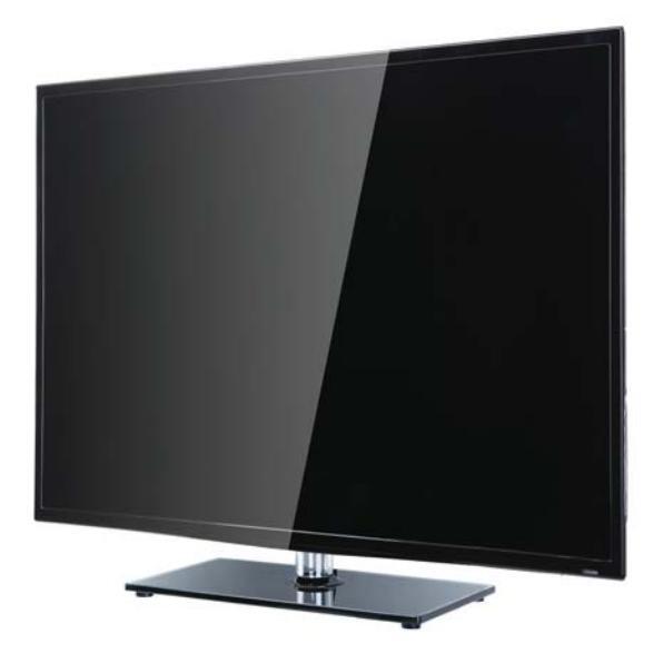
Haier SERVICE MANUAL
LED TV
Model No. LE42H6600CU
MSD308 Chassis

This service information is designed for experienced repair technicians only and is not designed for use by the general public. It does not contain warnings or cautions to advise non-technical individuals of potential dangers in attempting to service a product. Products powered by electricity should be serviced or repaired only by experienced professional technicians. Any attempt to service or repair the product or products dealt with in this service information by anyone else could result in serious injury or death.
©2011 Qingdao Haier Electronics Co., Ltd. All rights reserved. Unauthorized copying and distribution is a violation of law.
Haier Group
Chapter 1: General Information
1-1. Table of Contents
| 1. General Information 1 |
|---|
| 1-1. General Guidelines 3 |
| 1-2. Important Notice 3 |
| 1-3. How to Read this Service Manual 6 |
| 2. Specification |
| 3. Location of Controls and Components8 |
| 3-1. Board Location 8 |
| 3-2. Main Board 8 |
| 3-3. Power Board 14 |
| 3-4. LCD Panel 15 |
| 4. Disassemble and Assemble 17 |
| 5. Electrical Parts |
| 6. Trouble-shooting 23 |
| 7. Hotel Mode 34 |
| 8. Upgrade Instruction 35 |
1-1. General Guidelines
When servicing, observe the original lead dress. If a short circuit is found, replace all parts which have been overheated or damaged by the short circuit.
After servicing, see to it that all the protective devices such as insulation barriers, insulation papers shields are properly installed.
After servicing, make the following leakage current checks to prevent the customer from being exposed to shock hazards.
1) Leakage Current Cold Check
- 2) Leakage Current Hot Check
- 3) Prevention of Electro Static Discharge (ESD) to Electrostatically Sensitive
1-2. Important Notice
1-2-1. Follow the regulations and warnings
Most important thing is to list up the potential hazard or risk for the service personnel to open the units and disassemble the units. For example, we need to describe properly how to avoid the possibility to get electrical shock from the live power supply or charged electrical parts (even the power is off).
This symbol indicates that high voltage is present inside. It is dangerous to make any king of contact with any inside part of this product.
This symbol indicates that there are important operating and maintenance instructions in the literture accompanying the appliance.
1-2-2. Be careful to the electrical shock
To prevent damage which might result in electric shock or fire, do not expose this TV set to rain or excessive moisture. This TV must not be exposed to dripping or splashing water, and objects filled with liquid, such as vases, must not be placed on top of or above the TV.
1-2-3. Electro static discharge (ESD)
Some semiconductor (solid state) devices can be damaged easily by static electricity. Such components commonly are called Electrostatically Sensitive (ES) Devices. The following techniques should be used to help reduce the incidence of component damage caused by
1-2-4. About lead free solder (PbF)
This product is manufactured using lead-free solder as a part of a movement within the consumer products industry at large to be environmentally responsible. Lead-free solder
1-2-5. Use the genewing parts (specified parts)
Special parts which have purposes of fire retardant (resistors), high-quality sound (capacitors), low noise (resistors), etc. are used.
When replacing any of components, be sure to use only manufacture's specified parts shown in the parts list.
Safety Component
• Components identified by mark have special characteristics important for safety.
1-2-6 Safety Check after Repairment
Confirm that the screws, parts and wiring which were removed in order to service are put in the original positions, or whether there are the positions which are deteriorated around the serviced places serviced or not. Check the insulation between the antenna terminal or external metal and the AC cord plug blades. And be sure the safety of that.
General Servicing Precautions
1. Always unplug the receiver AC power cord from the AC power source before;
a. Removing or reinstalling any component, circuit board module or any other receiver assembly.
b. Disconnecting or reconnecting any receiver electrical plug or other electrical connection.
c. Connecting a test substitute in parallel with an electrolytic capacitor in the receiver.
CAUTION: A wrong part substitution or incorrect polarity installation of electrolytic capacitors may result in an explosion hazard.
2. Test high voltage only by measuring it with an appropriate high voltage meter or other voltage measuring device (DVM, FETVOM, etc) equipped with a suitable high voltage probe.
Do not test high voltage by "drawing an arc".
3. Do not spray chemicals on or near this receiver or any of its assemblies.
4. Unless specified otherwise in this service manual, clean electrical contacts only by applying the following mixture to the contacts with a pipe cleaner, cotton-tipped stick or comparable non-abrasive applicator; 10% (by volume) Acetone and 90% (by volume) isopropyl alcohol (90%-99% strength).
CAUTION: This is a flammable mixture.
Unless specified otherwise in this service manual, lubrication of contacts is not required. Capacitors may result in an explosion hazard.
5. Do not defeat any plug/socket B+ voltage interlocks with which receivers covered by this service manual might be equipped.
6. Do not apply AC power to this instrument and/or any of its electrical assemblies unless all solid-state device heat sinks are correctly installed.
7. Always connect the test receiver ground lead to the receiver chassis ground before connecting the test receiver positive lead.
Always remove the test receiver ground lead last. Capacitors may result in an explosion hazard.
8. Use with this receiver only the test fixtures specified in this service manual.
CAUTION: Do not connect the test fixture ground strap to any heat sink in this receiver.
9. Remove the antenna terminal on TV and turn on the TV.
10. Insulation resistance between the cord plug terminals and the eternal exposure metal should be more than Mohm by using the 500V insulation resistance meter.
11. If the insulation resistance is less than M ohm, the inspection repair should be required. If you have not the 500V insulation resistance meter, use a Tester. External exposure metal: Antenna terminal Headphone jack
Electrostatically Sensitive (ES) Devices
Some semiconductor (solid-state) devices can be damaged easily by static electricity. Such components commonly are called Electrostatically Sensitive (ES) Devices. Examples of typical ES devices are integrated circuits and some field-effect transistors and semiconductor "chip" components. The following techniques should be used to help reduce the neidence of component damage caused by static by static electricity.
1. Immediately before handling any semiconductor component or semiconductorequipped assembly, drain off any electrostatic charge on your body by touching a known earth ground. Alternatively, obtain and wear a commercially available discharging wrist strap device, which should be removed to prevent potential shock reasons prior to applying power to the unit under test.
2. After removing an electrical assembly equipped with ES devices, place the assembly on a conductive surface such as aluminum foil, to prevent electrostatic charge buildup or exposure of the assembly.
3. Use only a grounded-tip soldering iron to solder or unsolder ES devices.
4. Use only an anti-static type solder removal device. Some solder removal devices not classified as "anti-static" can generate electrical charges sufficient to damage ES devices.
5. Do not use freon-propelled chemicals. These can generate electrical charges sufficient to damage ES devices.
6. Do not remove a replacement ES device from its protective package until immediately before you are ready to install it.
(Most replacement ES devices are packaged with leads electrically shorted together by conductive foam, aluminum foil or comparable conductive material).
7. Immediately before removing the protective material from the leads of a replacement ES device, touch the protective material to the chassis or circuit assembly into which the device will be installed.
CAUTION: Be sure no power is applied to the chassis or circuit, and observe all other safety precautions.
8. Minimize bodily motions when handling unpackaged replacement ES devices. (Otherwise harmless motion such as the brushing together of your clothes fabric or the lifting of your foot from a carpeted floor can generate static electricity sufficient to damage an ES device.)
1-2-7. Ordering Spare Parts
Please include the following informations when you order parts. (Particularly the Version letter)
1. Model number, Serial number and Software Version The model number and Serial number can be found on the back of each product and the Software Version can be found at the Spare Parts List.
2. Spare Part No. and Description You can find them in the Spare Parts List
1-2-8. Photo used in this manual
The illustration and photos used in this Manual may not base on the final design of products, which may differ from your products in some way.
1-3. How to Read this Service Manual
Using Icons:
Icons are used to attract the attention of the reader to specific information. The meaning of each icon is described in the table below:
Note:
A "note" provides information that is not indispensable, but may nevertheless be valuable to the reader, such as tips and tricks.
Caution:
A "caution" is used when there is danger that the reader, through incorrect manipulation, may damage equipment, loose data, get an unexpected result or has to restart(part of) a procedure.
Warning:
A "warning" is used when there is danger of personal injury.
Reference:
A "reference" guides the reader to other places in this binder or in this manual, where he/ she will find additional information on a specific topic.
2. Specifications
| Model | LE42H6600CU |
|---|---|
| Screen Size | 41.6inch |
| Aspect Ratio | 16:9 |
| Resolution | 3840*2160 |
| Response Time (ms) | 9.5mS(G-to-G) |
| Angel of View | 178° |
| Color Display | 1.07G |
| OSD Language |
English/French/Italian/Spanish/Germany/Dutch/Russian/Polish
Czechic/Roumania/Hungary/Greek/Portuguese |
| Color System | PAL/SECAM |
| Audio System | BG/DK/I;L/L' |
|
Audio Output Power
(Built-in) (W) |
8W× 2 |
|
Audio Output Power
(outer) (W) |
No |
| Total Power Input (W) | 75W |
| Voltage Range (V) | AC100V-240V |
| Power Frequency (Hz) | 50Hz |
| Net Weight (KG) | 8.8 |
| Gross Weight (KG) | 9.8 |
| Net Dimension (MM) | 937*200*611 |
|
Packaged Dimension
(MM) |
1080*120*670 |
3. Location of Controls and Components
3-1 Board Location

| No. | Part Number | Description |
|---|---|---|
| A Board | DH1TQ0D0300M | Main board |
| B Board | 240403000476 | Power board |
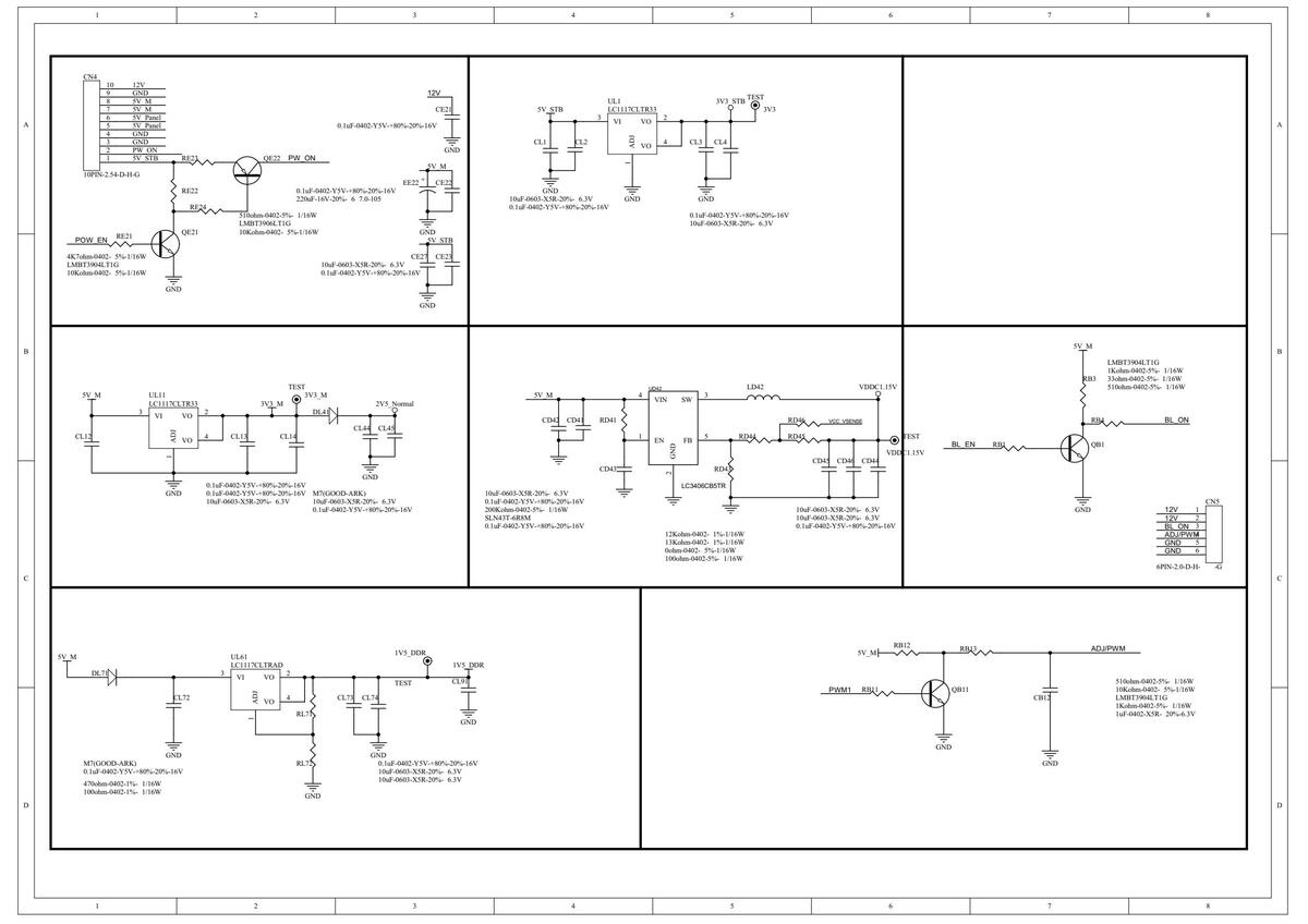
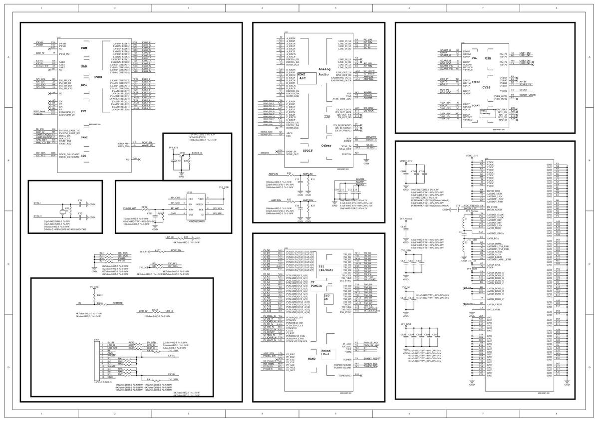
3-2 Main Board

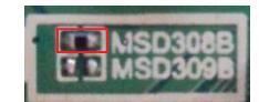
ENLARGED VIEW OF CHIPSET
As the picture shows in right, to differ the board and chipset
by resistance and mark.
FRONT VIEW OF T.MSD309.BTU87

SIDE VIEW OF T.MSD309.BTU87

Note2: The HDMI3 support MHL 2.0.
Note3: For HDMI3, MHL function is optional, and for HDMI1, ARC function is optional.
REQUIRET OF WIRE HARNESS

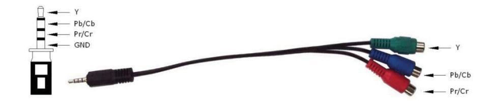
MINI YPbPr IN
3. FEATURES
| MSD309BT-SW (DVB-T) +MST6M40A+MSB101A(T2) | ||||||
|---|---|---|---|---|---|---|
| CHIPSET | MSD308BT-SW (D) | /B-T/C) +MS | 3-T/C) +MST6M40A +MSB101A(T2) | |||
| MSD308BT-SW (D) | /B-T/C) +MS - | Г6М40А | ||||
| MSD309BT-SW (D) | /B-T) +MST6 | M40A | ||||
| MARKET AREA | Pan Europe | |||||
|
OSD
LANGUAGE |
English, French, German, Italian, Spanish, Portuguese (optional) | |||||
| Panel Type | LED | |||||
| PANEL | Interface | Dual/Single LVDS Interface | ||||
| Max Resolution | 4K×2K | |||||
| Receiving Ra | ange | 48.25MHz ~ 863.25MHz | ||||
| Input Imped | lance | 75Ω | ||||
| Video Syste | m | PAL, SECAM | ||||
| ATV | BG, DK, I, L/L' | |||||
| Sound Syste | em | NICAM/A2 | ||||
| TELETEXT | 1000Pages | |||||
| Max Storage | e Channels | 100CH | ||||
| VHF (174MHz ~ 230MHz) | ||||||
| Receiving Range | UHF (474MHz ~ 862MHz) | |||||
| Input Impedance | 75Ω | |||||
| Channel Bandwidth | 7MHz/8MHz | |||||
| COFDM 2K/8K | ||||||
| TV INPUT | Modulation | QPSK,16QAM,64QAM | ||||
| DVB-T2 | QPSK,16QAM,64QAM,256QAM | |||||
| DVB-C | 160AM 220AM 640AM | |||||
| DTV | (only with | 1280AM 2560AM | ||||
| MSD308BT-SW) | ||||||
| Video System | MPEG-2 MP@ML, MPEG-2 | |||||
| MP@HL,H.264 | ||||||
| Sound System | MPEG-1 layer 1/2,MPEG-2 layer | |||||
| 2, DD,DD+ | ||||||
| Basic Functi | ons | EPG, Subtitle, LCN, TELETEXT | ||||
| Common Ind | (Europe) | |||||
| Max Storage | ||||||
| Format | Channels | |||||
| PC-KGD | Video Syste | m | ||||
| CVBS | Video Level | 1.0.1/2 + 10% | ||||
| VIDEO INPUT | Component | 480i 480n | 576i 576n 720n | 1080i 1080p | ||
| номі | 480i 480n | 576i 576p 720p | ||||
| SCART | CVBS & RGF | 3 | ||||
| PC Audio | Earphone In |
-
Iput |
0.2 ~ 2.0 Vpmg | |||
| AUDIO INPUT | CVBS/Component | |||||
| Audio | L/R RCA Inp | out | 0.2 ~ 2.0 V RMS | |||
|
Frequency
Response |
100Hz~15KHz @±3dB (1KHz, 0 | dB reference signal) | ||
|---|---|---|---|---|
| AUDIO | Amplifier power: 12V | 2×8W(8Ω) | ||
| OUTPUT | Max Output | Amplifier power: 24V | 2×9W(8Ω) | |
| Power | THD+N<10%@1KHz, Audio Input:0.5V RMS | |||
| POWER | Requirement | 12V/5V/5VSB | ||
| To Panel | 5V,12V | |||
| Management | Standby Power Consumption < 0.2W(Board Only) | |||
| COMB FILTER | 3D | |||
| DEINTERLACE | 3D | |||
| KEY FUNCTION | MENU, CH+, CH-, VOL+, VOL-, INPUT, POWER | |||
| EXPANDABLE | ||||
| FUNCTION | ||||
Note: Licenses involved in specifications above are supposed to be obtained by customers themselves. USB MULTIMEDIA PLAYBACK FORMAT
| Madia | Codec | Domork | |||
|---|---|---|---|---|---|
| места | File Ext. | Video | Audio | кетагк | |
| Max Solution: 1920×1080 | |||||
| .mpg | MPEG-1, MPEG-2 | Max Data Rate: 40 Mbps | |||
| DivX, Xvid, MJPEG, | |||||
| .avi | MPEG-4 SP/ASP, | ||||
| H.264 | |||||
| .ts | MPEG-2, H.264 | ||||
| .mov | MPEG-4 SP/ASP, | Max Solution: 1920×1080 | |||
| Movie | .mkv | H.264 | ACO,FCM | Max Data Rate: 20 Mbps | |
| novie | .dat | MPEG-1 | |||
| MPEG-4 SP/ASP, | |||||
| .mp4 | H.264 | ||||
| MPEG-1, MPEG-2 | Max Solution: 720×576 | ||||
| .vob | MPEG-2 | Max Data Rate: 40 Mbps | |||
| .rm | RV8/RV9/MP2 |
cook,
MP2 |
Max Solution: 1920×1080 | ||
| 1717 2 | |||||
| mn3 | MP3 | Sample Rate: 8K~48KHz | |||
| Bit Rate: 32K~320Kbps | |||||
| Music | .wma | WMA | Channel: Mono/Stereo | ||
| Music | Sample Rate: 16K~48KHz | ||||
| .m4a/.aac | AAC | Bit Rate: 32K~442Kbps | |||
| Channel: Mono/Stereo | |||||
| Photo | .jpg/ | Progressive | JPEG | Max Resolution: 1024×768 | |
| FIIOLO | .jpeg | Baseline J | PEG | Max Resolution: 8192×8192 | |
T.MSD309.BTU87(Europe)
| Max Resolution: 6500×6500 | |||
|---|---|---|---|
| .bmp | ВМР | Pixel Depth: 1/4/8/16/24/32 | |
| bpp | |||
| Non-Interlaced | Max Resolution: 3000×3000 | ||
| .png | Interlaced | Max Resolution: 1500×1500 | |
File system: Hi Speed FS, FAT32, FAT16, NTFS(NTFS compressed file is not supported).
PVR function: Recording standby, time-shift, EPG recording reservation.
Note: Licenses involved in specifications above are supposed to be obtained by customers themselves.
ELECTRICAL CHARACTERISTICS & REQUIREMENTS
| Symbol | Voltage Range | Ripple | Total | Each p | art of the | e MAX. cu | rrent(m | A) | ||
|---|---|---|---|---|---|---|---|---|---|---|
| Symbol | MIN | ТҮР | MAX | Voltage | current | Mainboard | AMP | USB | MHL | Panel |
| 12V | 11 | 12 | 13 | 120 mVP-P | 4000 | 100 | 1000 | 2500 | ||
| 5V | 4.9 | 5 | 5.25 | 50 mVP-P | 7000 | 4000 | 700×2 | 1200 | ||
| 5VSB | 4.9 | 5 | 5.25 | 50mVP-P | 2000 | 500 | 1200 | |||
|
24V AMP
POWER |
22 | 24 | 25 | 240 mVP-P | 1000 | 1000 | ||||
Note: The current of inverter and extension modules are not included in maximum current.
Note*: Don't exceed 5.25V when make the certification practice test.
The power supply for amplifier is optional, 12V or 24V

| Alternation | Description | MIN | МАХ | Unit |
|---|---|---|---|---|
| t1 | Startup time | 0 | 100 | mS |
| t2 | Rise time | 0 | 50 | mS |
| t3 | The drop time of voltage | 0 | 200 | mS |
SUBSTITUTABLE PRIMARY MATERIALS
The table is for reference only, the actual item is the standard.
| NAME | ТҮРЕ | BRAND | BACKUP TYPE | BACKUP BRAND | |
|---|---|---|---|---|---|
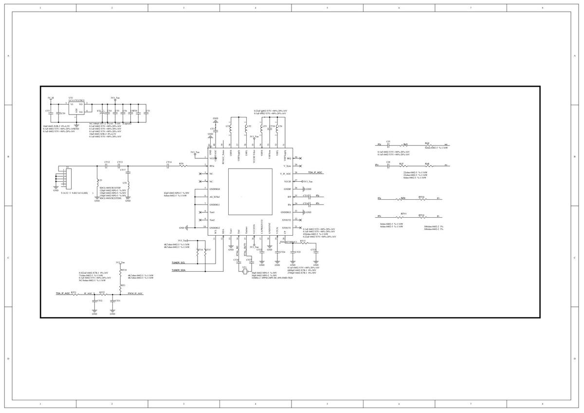
| TUNER | TDA18273HN | NXP | |||
| 000 | H5TQ1G63EFR-PBC | Hypix | K4B1C1646C-BCK0 | Comment | |
| DDR | (1G bits 1600MHz) | K4DIGI040G-DCK0 | Samsung | ||
| GIGA | W25Q32BVSSIG | Winbond | |||
|
FLASH FOR
309B |
GD25Q32BSIG
(32M bits) |
MX25L3206EM2I-12G | Macronix | ||
| S25FL032K0XMFI011 | Spansion | ||||
| GD25Q16SIP | GIGA | ||||
|
FLASH FOR
6M40 |
W25Q16DVSSIG | Winbond | MX25L1606EM2I-12G | Macronix | |
| EN25Q16-104HIP | EON | ||||
| AMPLIFIER | TAS5707 | TI | |||
4. PCB DIMENSIONS
The size of T.MSD309.BTU87 is 188.5mm(L)*190mm(W).

开模请以绿色定位孔为准
QR-ZZPJ-017
5. SCHEMATICS OF IR BOARD & KEY BOARD

6. INTERFACE DEFINITION
| NO. | SYMBOL | DESCRIPTION |
|---|---|---|
| 1 | VIN | |
| 2 | VIN | |
| 3 | VIN | |
| 4 | VIN | |
| 5 | VIN | Power input(+12V) |
| 6 | VIN | |
| 7 | VIN | |
| 8 | VIN | |
| 9 | NC | NO CONNECTION |
| 10 | GND | |
| 11 | GND | |
| 12 | GND | Ground |
| 13 | GND | |
| 14 | GND | |
| 15 | L/R_O | Output signal for Glasses Left Right signal |
*CNW1(51PIN/0.5): V-by-one HS for CHIMEI Connector
广州视源电子科技股份有限公司 Guangzhou Shiyuan Electronics Co.,Ltd.
| 16 | L/R | Input signal for Left/Right synchronous signal |
| 17 | 2D/3D | 2D/3D Enable |
| 18 | SDA | I2C Data signal |
| 19 | SCL | I2C Clock signal |
| 20 | NC | |
| 21 | NC | NO CONNECTION |
| 22 | LD_EN | Local Dimming Mode Enable |
| 23 | NC | |
| 24 | NC | NO CONNECTION |
| 25 | HTPDN | Hot plug detect output Open drain |
| 26 | LOCKN | Lock detect output Open drain |
| 27 | GND | Ground |
| 28 | Rx0n | V-by-One HS Data Lane0 |
| 29 | Rx0p | V-by-One HS Data Lane0 |
| 30 | GND | Ground |
| 31 | Rx1n | V-by-One HS Data Lane1 |
| 32 | Rx1p | V-by-One HS Data Lane1 |
| 33 | GND | Ground |
| 34 | Rx2n | V-by-One HS Data Lane2 |
| 35 | Rx2p | V-by-One HS Data Lane2 |
| 36 | GND | Ground |
| 37 | Rx3n | V-by-One HS Data Lane3 |
| 38 | Rx3p | V-by-One HS Data Lane3 |
| 39 | GND | Ground |
| 40 | Rx4n | V-by-One HS Data Lane4 |
| 41 | Rx4p | V-by-One HS Data Lane4 |
| 42 | GND | Ground |
| 43 | Rx5n | V-by-One HS Data Lane5 |
| 44 | Rx5p | V-by-One HS Data Lane5 |
| 45 | GND | Ground |
| 46 | Rx6n | V-by-One HS Data Lane6 |
| 47 | Rx6p | V-by-One HS Data Lane6 |
| 48 | GND | Ground |
| 49 | Rx7n | V-by-One HS Data Lane7 |
| 50 | Rx7p | V-by-One HS Data Lane7 |
| 51 | GND | Ground |
*CNW18(3PIN/2.0): IR CONNECTOR (Reserved)
| NO. | SYMBOL | DESCRIPTION | ||||
|---|---|---|---|---|---|---|
| 1 | GND | Ground | ||||
| 2 | IRE | Sync for 3D glasses (IR modulation Transfer) | ||||
| 3 | 3V3 | +3.3V Power Supply | ||||
◆ CN17(4PIN/2.54): AMPLIFIER POWER SUPPLY CONNECTOR
◆ CN18 (4PIN/2.54): SPEAKER CONNECTOR
| NO. | SYMBOL | DESCRIPTION |
|---|---|---|
| 1 | LOUT+ | Audio Left Channel Output+ |
| 2 | LOUT- | Audio Left Channel Output- |
| 3 | ROUT- | Audio Right Channel Output- |
| 4 | ROUT+ | Audio Right Channel Output+ |
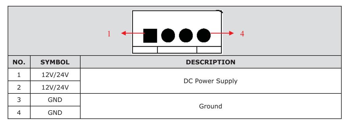
-▶ 6 NO. SYMBOL DESCRIPTION 1 +12V DC Power Supply 2 З 4 ADJ Brightness Adjustment for Panel 5 GND Ground 6 GND
◆ CN5(6PIN/2.0): INVERTER CONNECTOR
• CN4(10PIN/2.54): MAIN POWER SUPPLY CONNECTOR
| NO. | SYMBOL | DESCRIPTION | ||||
|---|---|---|---|---|---|---|
| 1 | 5VSB | +5V Power Supply when Standby | ||||
| 2 | PON | Power On/Off | ||||
| 3 | GND | Constant | ||||
| 4 | GND | Ground | ||||
| 5 | P5V | |||||
| 6 | P5V | +5V Power Supply for Panel | ||||
| 7 | 5V | |||||
| 8 | 5V | +5V DC Power Supply | ||||
| 9 | GND | Ground | ||||
| 10 | 12V | +12V DC Power Supply | ||||
◆ CN7(14PIN/2.0): IR& KEY BOARD CONNECTOR
| NO. | SYMBOL | DESCRIPTION | ||
|---|---|---|---|---|
| 1 | 5V | +5V DC Power Supply | ||
| 2 | RED | Red Indicator | ||
| 3 | GRN | Green Indicator | ||
| 4 | IR | IR Receiver | ||
| 5 | GND | Ground | ||
| 6 | K0 | Кеу0 | ||
| 7 | K1 | Key1 |
| 8 | K2 | Key2 |
| 9 | К3 | Кеу3 |
| 10 | K4 | Key4 |
| 11 | К5 | Key5 |
| 12 | K6 | Кеуб |
| 13 | K7 | Key7(Reserved) |
| 14 | GND | Ground |
Model No.:
3-3. Power Board

| 1. Power Supply Overview 电性能指标: | |||||
|---|---|---|---|---|---|
| 1.1 Table 1 Input Electrical Characteristics | 1.1 Table 1 Input Electrical Characteristics Overview (输入特性) | ||||
| Input voltage range 输入电压范围 | 90Vac-264Vac | ||||
| Normal voltage range 标准输入 | 100Vac-240Vac | ||||
| Frequency range 频率范围 | 50Hz/60Hz | ||||
| Max input AC current 满载输入电流 | 3Amax at full load condition | ||||
| Inrush current (cold start)浪涌电流(冷机) | 50Atyp peak, 120Vac; 100Atyp peak, 220Vac | ||||
| Efficiency (full load) 效率 | 80%min at 230Vac / maximum load | ||||
| PFC 功率因素(输出带额定负载) | |||||
| Leakage Current 泄漏电流 | Less Than 0.75mA, 230Vac input | ||||
| No-load Power Loss 空载功耗 | ≦0.5W 240Vac input at 5Vsb Output current≪25mA | ||||
| Input Fuse 输入保险额定值 | T3.15AH/250Vac | ||||
1.2 Output Eletrical Characteristics Overview (输出特性)
1.2.1 Table 2 Output Voltage, Current & Regulation. (输出调整率)
| Output Voltage | Regulation | Min current | Rated current | |
|---|---|---|---|---|
| 输出电压 | 调整率 | 最小电流 | 额定电流 | 峰值功率 |
| LED 33-38V | ±10% | 0.10A | 0.48A | |
| +24V | ±15% | 0.1 | 0. 6A | |
| +12V | ±10% | 0. 3A | 1. OA | ≤72₩ |
| +5. 0V | ±5% | 0. 3A | 1.5A | |
| +5. 0VSB | ±5% | 0. 02A | 0. 5A |
1.2.2 Table 3 DC Output Ripple & Noise. (输出波纹和噪声)
| Output Voltage | Ripple & Noise(Max) |
|---|---|
| +24V | 240mVp-p@25°C (VAC=100~264V) |
| +12V | 120mVp-p@25°C (VAC=100~264V) |
| +5.0V、+5.0VSB | 60mVp-p@25°C (VAC=100~264V) |
Note: 1)Measurements shall be made with an oscilloscopewith 20Mhz bandwidth .
示波器设置在20MHz带宽
2) Output shall be bypassed at the connector with a 0.1 uF ceramic capacitor and a47uF
electrolytic simulate system loading.
输出并联0.1uF的陶瓷电容和47uF的电解电容。
1.2.3 Output Transient Response. (输出动态响应)
Table 4. Test condition测试条件
| Voltage Tolerance Limit | Slew Rate | Load Change |
|---|---|---|
| Min. to 50% load and 50% to | ||
| +12V/±10% ;5.2V/5.0VSB±5% | 0.2A/uS | Max load |
| All output±10% | 0.2A/uS | Min. load to Max load |
Note: Transient response measurements shall be made with a load changing repetition rate of 50Hz to 10kHz. 以50~10KHz的频率跳变负载来测试。
| 1.2.4 Table 5 DC Output Hold-Up Time. (输出保持时间) | ||||||
| Output Voltage | 120Vac input | 220Vac input | ||||
| +24V | ≥5 mS | ≥10 mS | ||||
| +12V | ≥5 mS | ≥10 mS | ||||
| +5.0V 、+5 | 5.0VSB | ≥5 mS | ≥10 mS | |||
| Note: All of dc | output at full | load.所有输出带满载 | ||||
| 1.2.5 Table 6 D | C Output Ov | ershoot At Turn On & Turn Off | .(输出超调) | _ | ||
| Over shoot vol | tage(V)超调电压 | |||||
| Output Channel | Output(V) | Turn on开机 | Turn off关机 | |||
| +24 | +24 | 10% | 10% | |||
| +12V | +12V | 10% | 10% | |||
| +5.0V 、+5.0VSB | +5.0V | 10% | 10% | |||
| Note: All of dc o | output current | from Min. to Max测试时负载范围 | 1: 最小到最大 | |||
| 1.2.6 Table 7 I | OC output vol | ltage rise time(输出上升时间) | _ | |||
| Output Vo | oltage | 120Vac input | 220Vac input | |||
| +24V | T | ≤100 ms | ≤100 ms | |||
| +12V | T | ≤100 ms | ≤100 ms | |||
| +5.0V 、+5 | 5.0VSB | ≤100 ms | ≤100 ms | |||
|
The power supply DC outputs shall be enable with an active-high TTL
2.5V/2.0mA)-compatible signal(Ps-on). The 5.0Vsb is on whenever the AC power is present. 除5.0Vsb外,其余输出受控于一个TTL电平兼容的信号 (Ps-on≥2.5V/2.0mA) 5.0Vsb上电就存在。 * When Ps-on is pulled to TTL high, the DC outputs are to be enabled. Ps-on高电平,打开输出 * When Ps-on is pulled to TTL low or open circuit, the DC outputs are to be disabled. Ps-on低电平,关闭输出 Table 8. |
||||||
| Ps-on Signal | Comments | Outputs | ||||
| Ps-on- h | nigh | ≥2.5V&2.0mA ( source) | Output | |||
| Ps-on- 1 | ow | ≪0.5 V | Х | |||
| Ps-on-o | pen | — | Х | |||
| 1.4 Protection:(保护功能) 1.4.1 Table9 DC Over Voltage Protection. (输出过压保护) The power supply have the over voltage protection. When the main feedback control circuit fault occur . The power supply shall be over voltage protection to protect the whole system. 该开关电源具有过压保护功能,当主反馈回路出现故障时,电源过压保护,从而保护整个系统安全) | ||||||
第6页,共12页
| 1.4.2 Table 10 DC Output Over current Protection. (输出过流保护) | ||||
|---|---|---|---|---|
| Output Voltage | Over Current | Comments | ||
| +24V | ≥1.5A | |||
| +12V | ≥2.5A | Hiccup尝试重复启动 | ||
| +5.0V | ≥4.2A | Hiccup尝试重复启动 | ||
| +5.0VSB | ≥4. 2A | Hiccup尝试重复启动 | ||
1.4.3 Table 11 DC Output Short Circuit Protection. (输出短路保护)
| Output Voltage | Comments |
|---|---|
| +24V | Hiccup尝试重复启动 |
| +12V | Hiccup尝试重复启动 |
| +5.0VSB | Hiccup尝试重复启动 |
Note:* The Short Circuit protection should be test at other of dc output at min load 短路保护测试是在其它最小负载时测试.
1.4.4 Reset After Shutdown. (保护功能复位)
Recycle the ps-on signal, the power supply will restart after the fault removed.
故障去除后,关掉Ps-on信号再打开,电源即可恢复。
1.5 LED General Requirements (LED 电气性能)
151 Table 1 Output Electrical Characteristics Overview 硷出特性)
| 1.5.1 Tuble 1 Output Electrical Characteristics Overview (mili 1) [L] | ||||||
|---|---|---|---|---|---|---|
| PARA METER | SYMBOL | MIN | TYPICAL | MAX | UNIT | REMARK |
| 参数 | 符号 | 最小值 | 典型值 | 最大值 | 单位 | 备 注 |
| LED VOLTAGE | VLFD | 33 | 36 | 38 | V | |
| LED电压 | VEED | 50 | • | |||
|
LED CURRENT
LED电流 |
ILED | - | 480 | - | mA | Per string |
|
Power consumption
消耗功率 |
PBL | - | 35 | 40 | W | Full brightness |
|
Backlight ON/OFF
control |
Von/off | - | 0 | 0.5 | V | Off State |
| BL-ON开关电压 | V OII/OII | 2.5 | 5 | 5. 5 | v | On State |
| PWM Dimming mode | ADJ | 20 | - | 100 | % | PWM dimming mode |
|
EFFICIENCY
效率 |
Eff | 80 | - | - | % | Full brightness |
| 1.5.2 LED Protect | 1.5.2 LED Protection:(保护功能) | |||||
| Ducto sticu Clear | Description | REMARK | ||||
| Protection Characteristics | Description | 备 | 注 | |||
| LED Open Protection: | Shutdown and no damage | Per s | tring | |||
| LED String Short Protection: | Shutdown and no damage | Per s | tring | |||
| LED Over-Voltag | ge Protection: | L | ED Voltage≪50V | V | ||
| 2.Pin Connection(连接 | 器脚位定义) | |||
|---|---|---|---|---|
| Power supply connectors (电源 | 原输入/输出端子)AC INPUT(交流输入 | ) | ||
| Location (位置): CON01 | ||||
| Connector type (端子型号):3 | .96mm-3Pin | |||
| Pin assignments: Table. | ||||
| Pin No | Symbol | Description | ||
| (引脚号) | (符号) | (描述) | ||
| 1 | L | |||
| 2 | NC | |||
| 3 | Ν | |||
| Table 12 Pin-CON201 Cor | nnection And Function TYPE | : 4PIN-2.5mm | ||
|
Pin No
(己即是) |
Symbol
(符号) |
Description
(描述) |
||
| 1.9 | +24V | |||
| 2.4 | ||||
| 0.4 | GIVD | TZ4V DC GROUND | ||
| Table 13 Pin-CON200 Co | nnection And Function TYPE : | 13PIN-2.5mm | ||
| NO. | Pin Connection | Function | ||
| 1 | GND | +5VSB&+5V DC GROUND | ||
| 2 | GND | +5VSB&+5V DC GROUND | ||
| 3 | +5V | +5VDC OUTPUT | ||
| 4 | +5V | +5VDC OUTPUT | ||
| POWER ON/OFF CONTROL | ||||
| 5 | PS_ON | (ON = HIGH LEVEL) | ||
| 6 | +5VSB | STANDBY OUTPUT | ||
| 7 | +5V | +5V DC OUTPUT | ||
| 8 | +5V | +5V DC OUTPUT | ||
| 9 | GND | +12V DC GROUND | ||
| 10 | GND | +12V DC GROUND | ||
| 11 | GND | +12V DC GROUND | ||
| 12 | 12V | +12V DC OUTPUT | ||
| 13 | 12V | +12V DC OUTPUT | ||
| Table 15 Pin-CON02 Conne | ection And Function TYPE : 4P | IN-2.0mm | ||
| NO. | Pin Connection | Function | ||
| 1 | ON/OFF | LED CONTROL(ON = HIGH LEVEL) | ||
| 2 | ADJ | 输入PWM调光控制信号 | ||
| 3 | GND | GROUND | ||
| 4 | GND | GROUND | ||
| Location(位置): CN101, | CN102 | _ | _ | |||
| Connector type (端子型号): | PH2.0mm/2Pin or | equivalent | t | |||
| Pin No(引脚号) | Symb | ol(符号) | Description(描述) | |||
| 1 | LEI | D+ | LED+ | |||
| 2 | LE | D- | LED- | |||
| 3. Isolation (绝缘性能) | ||||||
| 3.1 Table 16 (绝缘性能) | ||||||
| Input To Output | DC5 | 00V 50MΩ Min (at room temperature) | ||||
| Note: | ||||||
| 3.2 Table 17 (绝缘耐压) | ||||||
| Input To Output | AC 3.0KV/10mA 50Hz 1 minute | |||||
| Note: | 1 | |||||
| 4. Safety (安全规格) | ||||||
| The power supply shall com | pliance with the fo | ollowing Cr | riterion | : | ||
| 电源安全性满足下列标准 | - | |||||
| 1) IEC60950、UL60950、 | IEC60065、GB4 | 943-2001 | ||||
| 5. EMC (电磁兼谷性) | ||||||
| 5.1 EMI(电磁十九) | 1 0 11 . | |||||
| The power supply shall 电源电磁干扰满足下列 |
compliance with t
可规则: |
he followin | ng Crite | rion: | ||
| 1) Conduction Emissio | n:(传导干扰度) | |||||
| EN55022, CLAS | SS B | |||||
| GB9254,CLASS | В | |||||
| FCC PART15 CI | LASS B | |||||
| 2) Radiate Emission:(辐 | 射干扰度) | |||||
| EN55022, CLAS | SS B | |||||
| GB9254,CLASS | В | |||||
| FCC PART15 CI | FCC PART15 CLASS B | |||||
| 5.2 EMS(电磁干扰) | ||||||
The power supply shall compliance with the following Criterion:
|
||||||
|
*GB1/626.4-1998/IEC6
3) Surge (雷击浪涌) |
*GB17626.4-1998/IEC61000-4-4 3KV ±1kV (瞬时测试), ±2kV (AC line noise)
3) Surge (雪志浪通) |
|||||
| *GB17626.5-1998/IEC61000-4-5 ±1KV | ||||||
第9页,共12页
| 6. Environmental Requirement (工作 3 | 不境) |
|---|---|
| 6.1 Temperature (环境温度) | |
| Operating : 0°C to +35°C | |
| Store: -10°C to +70°C | |
| 6.2 Humidity (环境温度) | |
| Operating : From10% to 90% relation | ive humidity (non-condensing). |
| Store: From 5 to 95% relative humic | lity (non-condensing). |
| 6.3 Altitude (海拔高度) | |
| Operating: Less than 2000m (仅适用- | 于在海拔2000米以下条件下使用) |
| 6.4 Cooling Method (冷却方式) | |
| Ventilation cooling . | |
| 6.5 Vibration (振动耐受) | |
| * 10-55Hz 29.4m/s2(3G),3minutes per | riod, 60minutes each along X, Y and Z axis. |
| 6.6 Impact (冲击耐受) | |
| *196.1m/s2(20G), 11mS, once each X | , Y and Z axis. |
| 6.7 Climates (气候要求) | |
| For moderate climates (适用于非热情 | 带气候) |
| 7.Dimension(物理尺寸) | |
| * 180mm X 117mm X 13mm 佚L *宽W | *高H).*高是指PCB上的高度 |
| 8.Weight (重量) | |
| * 500克 | |
| 备注: 带"*"的为参考项. | |

3-4. LED Panel
V420DK1-LS1 is a 42" TFT Liquid Crystal Display module with LED Backlight unit and 4ch-LVDS interface. This module supports 3840 x 2160 Quad Full HDTV format and can display true 1.07G colors (8-bit+FRC). The driving board module for backlight is built-in.
- High brightness 300 nits
- High contrast ratio 5000:1
- Fast response time Gray to Gray typical : 6.5 ms
- High color saturation NTSC 72%
- Quad Full HDTV (3840 x 2160 pixels) resolution, true HDTV format
- LVDS (Low Voltage Differential Signaling) interface
- Optimized response time for 100Hz/120Hz frame rate
- Viewing Angle : 176(H)/176(V) (CR>20) VA Technology
- Ultra wide viewing angle: Super MVA technology
- RoHs compliance
- T-con input frame rate : FHD 50/60Hz, FHD 100/120Hz or QFHD 24/30Hz Output frame rate: QFHD 50/60Hz, QFHD 100/120Hz or QFHD 48/60Hz
BLOCK DIAGRAM OF INTERFACE TFT LCD MODULE

INPUT TERMINAL PIN ASSIGNMENT
TFT LCD MODULE
CNF1 Connector Pin Assignment (187059-51221(P-TWO) or WF23-402-5133 (FCN))
Matting connector: FI-RE51HL (JAE)
| Pin | Name | Description | Note | |
|---|---|---|---|---|
| 1 | N.C. | No Connection | (1) | |
| 2 | SCL | I2C Clock (for mode selection & function setting) | ||
| 3 | SDA | I2C Data (for mode selection & function setting) | ||
| 4 | N.C. | No Connection | (1) | |
| 5 | L/R_O | Output signal for Left Right Glasses control | ||
| 6 | N.C. | No Connection | (1) | |
| 7 | SELLVDS | Input signal for LVDS Data Format Selection | (3)(9) | |
| 8 | N.C. | No Connection | ||
| 9 | N.C. | No Connection | ||
| 10 | N.C. | No Connection | ||
| 11 | GND | Ground | ||
| 12 | CH1[0]- | First pixel Negative LVDS differential data input. Pair 0 | ||
| 13 | CH1[0]+ | First pixel Positive LVDS differential data input. Pair 0 | ||
| 14 | CH1[1]- | First pixel Negative LVDS differential data input. Pair 1 | (4) | |
| 15 | CH1[1]+ | First pixel Positive LVDS differential data input. Pair 1 | ||
| 16 | CH1[2]- | First pixel Negative LVDS differential data input. Pair 2 | ||
| 17 | CH1[2]+ | First pixel Positive LVDS differential data input. Pair 2 | ||
| 18 | GND | Ground | ||
| 19 | CH1CLK- | First pixel Negative LVDS differential clock input. | (4) | |
| 20 | CH1CLK+ | First pixel Positive LVDS differential clock input. | (4) | |
| 21 | GND | Ground | ||
| 22 | CH1[3]- | First pixel Negative LVDS differential data input. Pair 3 | ||
| 23 | CH1[3]+ | First pixel Positive LVDS differential data input. Pair 3 | (4) | |
| 24 | CH1[4]- | H1[4]- First pixel Negative LVDS differential data input. Pair 4 | ||
| 25 | CH1[4]+ | First pixel Positive LVDS differential data input. Pair 4 | ||
| 26 | 2D/3D | Input signal for 2D/3D Mode Selection | ||
| 27 | L/R | Input signal for Left Right eye frame synchronous | ||
| 28 | CH2[0]- | CH2[0]- Second pixel Negative LVDS differential data input. Pair 0 | ||
| 29 | CH2[0]+ | Second pixel Positive LVDS differential data input. Pair 0 | ||
|---|---|---|---|---|
| 30 | CH2[1]- | Second pixel Negative LVDS differential data input. Pair 1 | ||
| 31 | CH2[1]+ | Second pixel Positive LVDS differential data input. Pair 1 | ||
| 32 | CH2[2]- | Second pixel Negative LVDS differential data input. Pair 2 | ||
| 33 | CH2[2]+ | Second pixel Positive LVDS differential data input. Pair 2 | ||
| 34 | GND | Ground | ||
| 35 | CH2CLK- | Second pixel Negative LVDS differential clock input. | ||
| 36 | CH2CLK+ | 2CLK+ Second pixel Positive LVDS differential clock input. | ||
| 37 | GND | Ground | ||
| 38 | CH2[3]- | Second pixel Negative LVDS differential data input. Pair 3 | ||
| 39 | CH2[3]+ Second pixel Positive LVDS differential data input. Pair 3 | |||
| 40 | CH2[4]- | H2[4]- Second pixel Negative LVDS differential data input. Pair 4 | ||
| 41 | CH2[4]+ | Second pixel Positive LVDS differential data input. Pair 4 | ||
| 42 | LD_EN | Input signal for Local Dimming Enable | (7)(9) | |
| 43 | N.C. | No Connection | (8) | |
| 44 | GND | Ground | ||
| 45 | GND | Ground | ||
| 46 | GND | Ground | ||
| 47 | N.C. | No Connection | (1) | |
| 48 | VCC | +12V power supply | ||
| 49 | VCC | +12V power supply | ||
| 50 | VCC | +12V power supply | ||
| 51 | VCC | +12V power supply | ||
CNF2 Connector pin assignment (187060-41221 (P-TWO) or WF23-400-413C (FCN))
Matting connector: FI-RE41HL (JAE)
| Pin | Name | Description | Note |
|---|---|---|---|
| 1 | N.C. | No Connection | (1) |
| 2 | N.C. | No Connection | |
| 3 | N.C. | No Connection | |
| 4 | N.C. | No Connection | |
| 5 | N.C. | No Connection | |
| 6 | N.C. | No Connection |
| 7 | N.C. | No Connection | ||
|---|---|---|---|---|
| 8 | N.C. | No Connection | ||
| 9 | GND | Ground | ||
| 10 | CH3[0]- | Third pixel Negative LVDS differential data input. Pair 0 | ||
| 11 | CH3[0]+ | Third pixel Positive LVDS differential data input. Pair 0 | ||
| 12 | CH3[1]- | Third pixel Negative LVDS differential data input. Pair 1 | ||
| 13 | CH3[1]+ | Third pixel Positive LVDS differential data input. Pair 1 | (4) | |
| 14 | CH3[2]- | Third pixel Negative LVDS differential data input. Pair 2 | ||
| 15 | CH3[2]+ | Third pixel Positive LVDS differential data input. Pair 2 | ||
| 16 | GND | Ground | ||
| 17 | CH3CLK- | Third pixel Negative LVDS differential clock input. | (4) | |
| 18 | CH3CLK+ | Third pixel Positive LVDS differential clock input. | (4) | |
| 19 | GND | Ground | ||
| 20 | СН3[3]- | Third pixel Negative LVDS differential data input. Pair 3 | ||
| 21 | CH3[3]+ | Third pixel Positive LVDS differential data input. Pair 3 | (4) | |
| 22 | CH3[4]- | Third pixel Negative LVDS differential data input. Pair 4 | (4) | |
| 23 | CH3[4]+ | Third pixel Positive LVDS differential data input. Pair 4 | ||
| 24 | GND | Ground | ||
| 25 | GND | Ground | ||
| 26 | CH4[0]- | Fourth pixel Negative LVDS differential data input. Pair 0 | ||
| 27 | CH4[0]+ | Fourth pixel Positive LVDS differential data input. Pair 0 | ||
| 28 | CH4[1]- | Fourth pixel Negative LVDS differential data input. Pair 1 | ||
| 29 | CH4[1]+ | Fourth pixel Positive LVDS differential data input. Pair 1 | (4) | |
| 30 | CH4[2]- | - Fourth pixel Negative LVDS differential data input. Pair 2 | ||
| 31 | CH4[2]+ | Fourth pixel Positive LVDS differential data input. Pair 2 | ||
| 32 | GND | Ground | ||
| 33 | CH4CLK- | Fourth pixel Negative LVDS differential clock input. | ||
| 34 | CH4CLK+ | Fourth pixel Positive LVDS differential clock input. | (4) | |
| 35 | GND | Ground | ||
| 36 | CH4[3]- | Fourth pixel Negative LVDS differential data input. Pair 3 | (4) | |
| 37 | CH4[3]+ | + Fourth pixel Positive LVDS differential data input. Pair 3 | ||
| 38 | CH4[4]- | Fourth pixel Negative LVDS differential data input. Pair 4 | ||
| 39 | CH4[4]+ | Fourth pixel Positive LVDS differential data input. Pair 4 | ||
| 40 | GND | Ground | ||
| 41 | GND | Ground | ||
4. Disassemble and assemble
Front

Back

4-1, Remove the 5 screws as below picture

4-2, Remove the 18 screws on the back cabinet

4-3, Remove the 5 screws on the back cabinet.

4-4, Remove the key board from the back cabinet.


5.Electrical Parts


T.MSD309.BTU87C Maintenance Manual

1. Power supply Trouble

2. Display Trouble(abnormal screen)

3. Audio Trouble(no sound)

4. Function Trouble(ATV/DTV)

5. Function Trouble(DVB-T/T2)

6. Function Trouble(PC)
7. Function Trouble(HDMI, YPbPr, SCART, CVBS)

7.Hotel Mode
Please press MENU key first, and then press number key "1001" to enter into Hotel Mode.
| PICTURE | Hotel Mode | Off | On | N | ||
|---|---|---|---|---|---|---|
| SOUND | Source Lock | × | ||||
| Default Source | Off | |||||
| 0 | CHANNEL | |||||
| Default Volume | 30 | |||||
| * | OPTION | Max Volume | 100 | |||
| Import Database | ||||||
| LOCK | ||||||
| 📖 Back | 🕀 Select | 💷 Exit |
Hotel Mode :
Hotel mode is set "ON", these below functions will be unavailable.
- Auto Tuning
- Color temperature
- Balance
- Sound mode
- Auto Volume
- Manual Tuning
- Clock
Source lock : you can't select the sources, which are set to "on ".
Default Source: Choose source, the options as follow:ATV/DTV/AV/PC/SCART/YPbPr/HDMI1/HDMI2/HDMI3 /USB,press the ▼▲ button to select the desired source, and press"OK" to comfirm.
Default Prog: In ATVmode, you can select a channel number to be set as the TV present channel. Press the ◄ ► button to select the desired channel number
Default Volume: Set default volume.
Max Volume: Set max volume limitted. This option allows you to set the Max Volume Level.
Import Database: You can use the U disk to import the Source lock / Default Source / Default Prog / Default Volume/ Max Volume database.
Export Database: You can use the U disk to export the Source lock / Default Source / Default Prog / Default Volume/ Max Volume database.
Clear lock: Clear Source lock / Default Source / Default Prog / Default Volume/ Max Volume set
Service Manual Model No.:
8. Upgrade Instruction
1. decompress the Software, the File usually named as "CVT_308B.bin"
2. copy "CVT_308B.bin" to the root of your U disk.
3. Plug the U disk to the TV USB terminal
4.Power on the TV, and the system will upgrade auto. while updating, the indicator LED light will flash slowly. when finished the light flash quikly. it will take 1~2mins.
NOTE:
Do not power off during the updating; Before turn on the TV again, please pull out the U disk from TV first.
Sincere Forever

Haier Group
Haier Industrial Park, No.1, Haier Road 266101, Qingdao, China http://www.haier.com
Printed in China


 Loading...