Service Document
Exchange Set
YACHT BOY 80 WR5408 PLL
Service
Manual
Sicherheit
Safety
Materialnr./Part No.
720108000001
Dieses Service Dokument ist nur in Datenform verfügbar
This Service Document is only available as data
Änderungen vorbehalten/Subject to alteration
Made by GRUNDIG in Germany • HS-41 0404
http://www.grundig.com
Es gelten die Vorschriften und Sicherheitshinweise
gemäß dem Service Manual "Sicherheit", Material-
S
nummer 720108000001, sowie zusätzlich die eventuell abweichenden, landesspezifischen Vorschriften!
The regulations and safety instructions shall be
valid as provided by the "Safety" Service Manual,
S
part number 720108000001, as well as the
respective national deviations.
ǵ

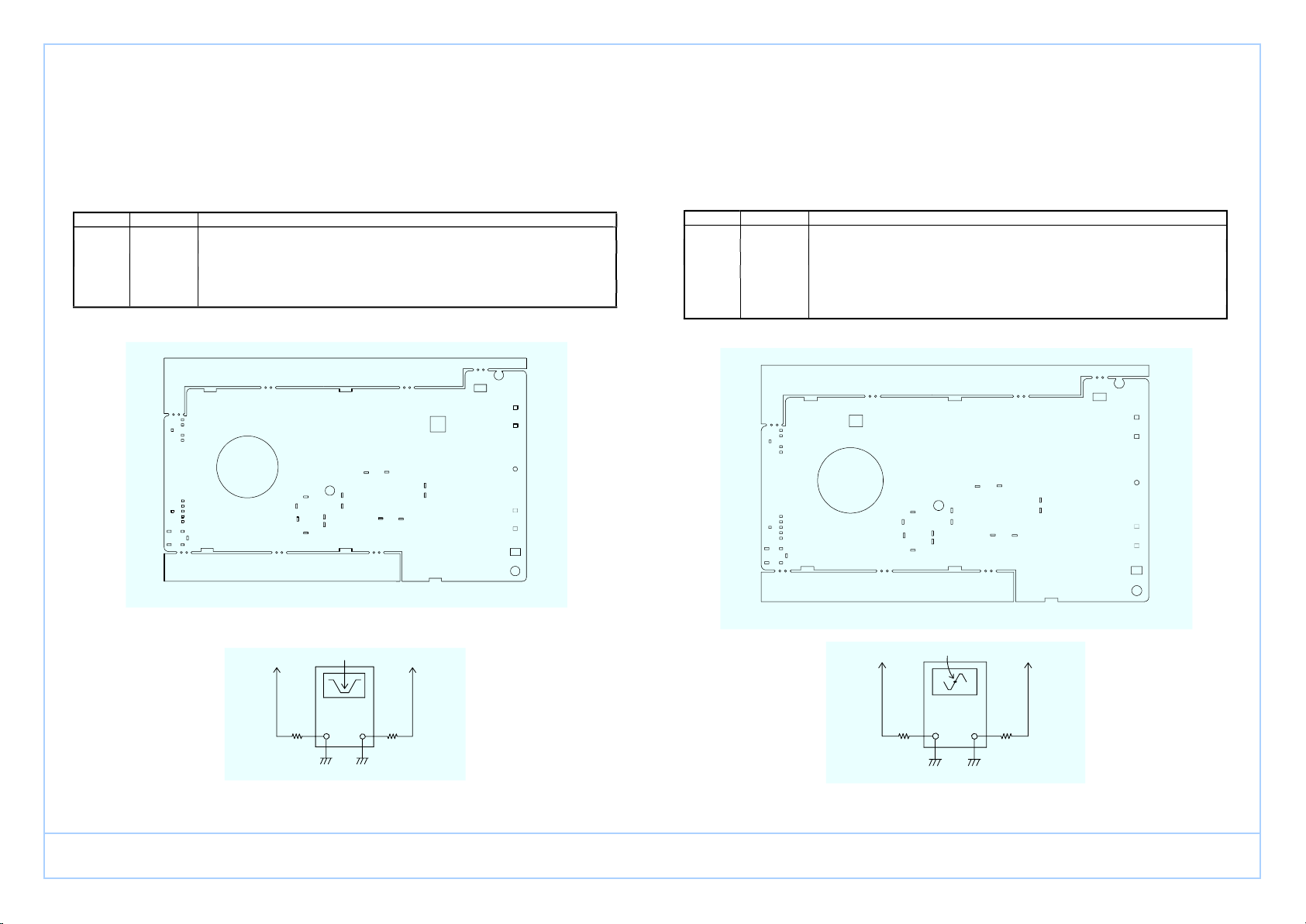
ALIGNMENT INSTRUCTIONS
(1) ALIGNMENT FOR AM IF
a. Required Instruments
AM IF Sweep Generator with Scope
b. Alignment Procedure
Mode Adjustment Procedure
(1) Turn on the radio.
(2) Connect the input of the AM IF sweep generation in series with a resister of 1.2K
Ohm to the test point TP2 and TP7.
(3) Connect the RF output of the AM IF sweep generation in series with a resister of
2.2K ohm to another test point TP3.
AM T2
(4) Adjust T2 to have a max. output and best center marker frequency to 450kHz.
c. Instrument Connection
T2
IN
OUT
1.2K
2.2K
RF
FM IF Sweep Generator
450KHz Marker
Test Point
TP2
Test Point
TP3
(2) ALIGNMENT FOR FM IF
a. Required Instruments
FM IF Sweep Generator with Scope
b. Alignment Procedure
Mode Adjustment Procedure
(1) Turn on the radio.
(2) Connect the input of the FM IF sweep generation in series with a resister of 1.2k
Ohm to the test point TP4 and TP7.
(3) Connect the RF output of the FM IF sweep generation in series with a resister of
2.2k ohm to another test point TP5.
(4) Adjust T1 have a max. output and best symmetrical S curve with respect to the
FM T1
Center marker frequency of 10.7MHz.
c. Instrument Connection
T1
RF
1.2K
IN
2.2K
OUT
Test Point
TP4
Test Point
TP5
FM IF Sweep Generator
10.7MHz Marker
ǵ
YACHT BOY 80

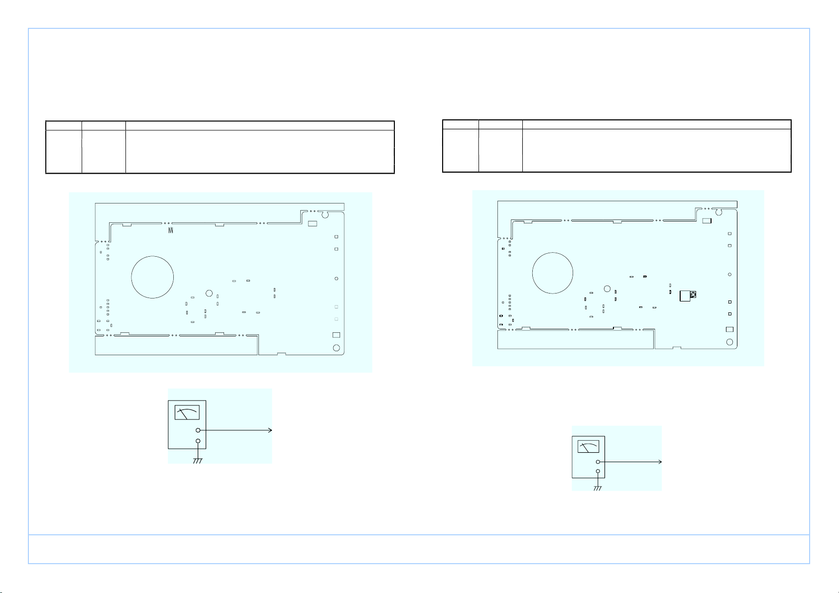
(3) ALIGNMENT FOR FM VOLTAGE TUNING RANGE
a. Required Instruments
DVM
b. Alignment Procedure
Mode Adjustment Procedure
(1) Set the power switch to ON.
(2) Set “ 108 MHz”.
(3) Connect at to the test point TP6 and TP7.
(4) Adjust L2 for show on 8.5V.
L2
(5) Set “87.5MHz” and check on DVM between 2.2V – 2.7V.
c. Instrument Connection
L2
Test Point TP6
DVM
(4) ALIGNMENT FOR AM VOLTAGE TUNING RANGE
a. Required Instruments
DVM
b. Alignment Procedure
Mode Adjustment Procedure
(1) Set the power switch to ON.
(2) Set “ 520 kHz”.
(3) Connect at to the test point TP6 and TP7.
(4) Adjust T10 for show on 1.10V.
T10
VC4
(5) Set “1710 kHz” and adjust VC4 for DVM show on 8.5V.
c. Instrument Connection
VC4
T10
Test Point TP6
DVM
ǵ
YACHT BOY 80

(5) ALIGNMENT FOR LW VOLTAGE TUNING RANGE
a. Required Instruments
DVM
b. Alignment Procedure
Mode Adjustment Procedure
(1) Set the power switch to ON.
(2) Set “ 153 kHz”.
(3) Connect at to the test point TP6 and TP7.
(4) Adjust T11 for show on 1.20V.
T11
VC5
(5) Set “279 kHz” and adjust VC5 for DVM show on 5.00.
c. Instrument Connection
VC5
T11
Test Point TP6
DVM
(6) ALIGNMENT FOR FM SENSITIVITY
a. Required Instruments
FM Signal Generator
SSVM
b. Alignment Procedure
Mode Adjustment Procedure
(1) Set the power switch to ON.
(2) Connect a SSVM to the test point TP8 and TP9.
(3) Connect the output of the FM signal generator to the test point TP5 and TP7.
(4) Set FM 90 MHz.
(5) Adjust L1 to have a max. Audio output.
(6) Set FM 106 MHz.
(7) Adjust VC1 to have a max. Audio output.
L1
VC1
(8) Repeat steps 4-7 until best sensitivity on these two frequency is formed.
c. Instrument Connection
L1
VC1
Test Point TP5
FM Signal Generator
Test Point TP8
SSVM
ǵ
YACHT BOY 80

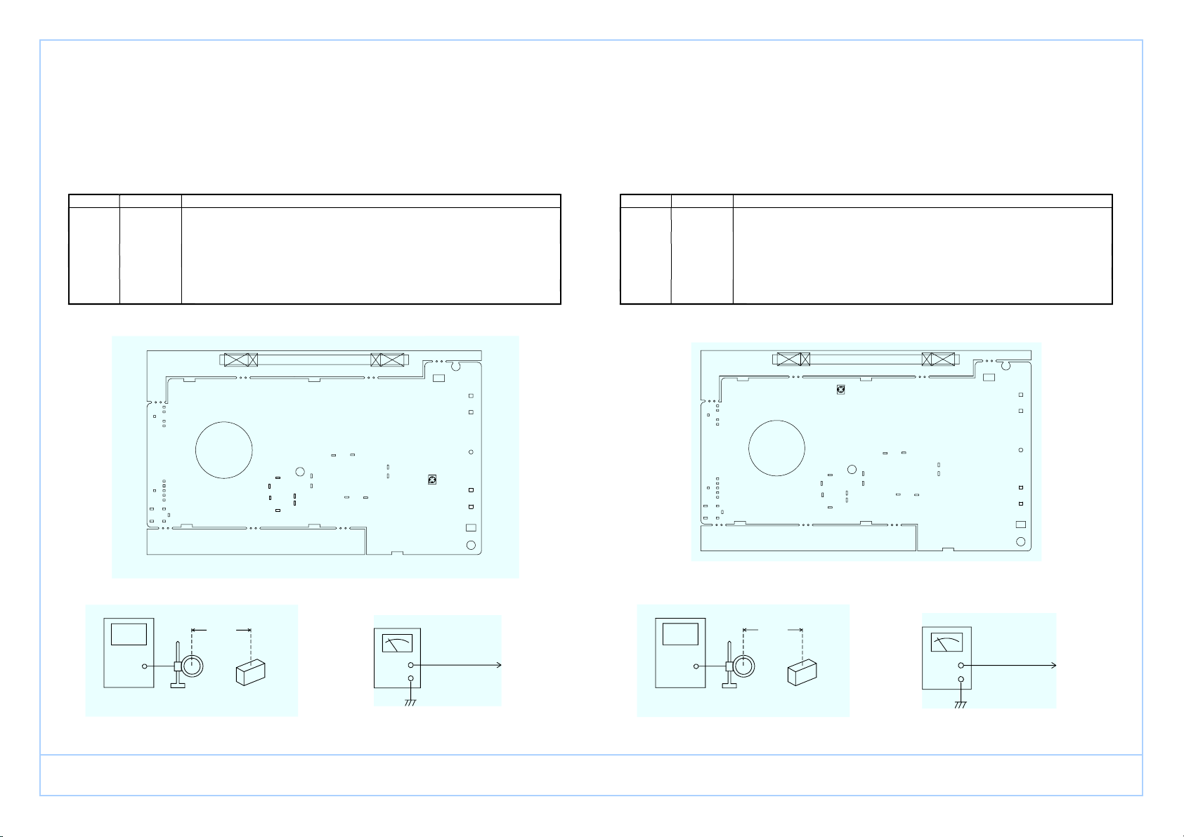
(7) ALIGNMENT FOR AM SENSITIVITY
a. Required Instruments
AM Signal Generator
SSVM
b. Alignment Procedure
Mode Adjustment Procedure
(1) Set the power switch to ON.
(2) Connect a SSVM to the test point TP8 and TP9.
(3) Connect the output of the FM signal generator to the test point TP8 and TP9.
(4) Set AM 600 kHz.
(5) Adjust L19A to have a max. Audio output.
(6) Set AM 1400 kHz.
(7) Adjust VC2 to have a max. Audio output.
L19A
VC2
(8) Repeat steps 4-7 until best sensitivity on these two frequency is formed.
c. Instrument Connection
A
L19
VC2
Loop Antenna
The radio is located
perpendicularly to
the Loop Antenna
60 cm
AM Signal Generator
Test Point TP8
SSVM
(8) ALIGNMENT FOR LW SENSITIVITY
a. Required Instruments
AM Signal Generator
SSVM
b. Alignment Procedure
Mode Adjustment Procedure
(1) Set the power switch to ON.
(2) Connect a SSVM to the test point TP8 and TP9.
(3) Connect the output of the AM signal generator to a standard loop antenna.
(4) Set LW 162 kHz.
(5) Adjust L19B to have a max. Audio output.
(6) Set LW 270 kHz.
(7) Adjust VC3 to have a max. Audio output.
L19B
VC3
(8) Repeat steps 4-7 until best sensitivity on these two frequencies is formed.
c. Instrument Connection
B
L19
VC3
Loop Antenna
The radio is located
perpendicularly to
the Loop Antenna
60 cm
AM Signal Generator
Test Point TP8
SSVM
ǵ
YACHT BOY 80

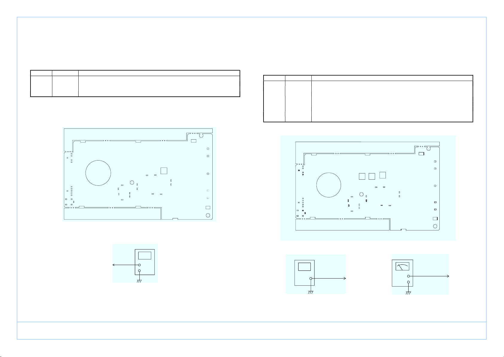
(9) ALIGNMENT FOR SW 2
ND LOCAL OSC
a. Required Instruments
Frequency counter with higher impedunce probe
b. Alignment Procedure
Mode Adjustment Procedure
(1) Turn the radio ON.
(2) Turn the frequency for away from any station to avoid interference.
(3) Connect the test probes of frequency counter to TP10 and TP7.
AM T8
(4) Adjust T8 to have a reading of 20.9898 – 20.9902 MHz.
Coution : a loading effect could emerge in the circuit if inserted with a lower impedance probe of frequency
Counter.
c. Instrument Connection
T8
Freq. Counter
Test Point
TP10
(10) ALIGNMENT FOR SW SENSITIVITY
a. Required Instruments
AM Signal Generator
SSVM
b. Alignment Procedure
Mode Adjustment Procedure
(1) Turn on the radio.
(2) Tune the radio band frequency to 15.100 MHz.
(3) Feed a signal with modulation from the AM signal generator output to tese point
TP5 and connect a SSVM to the speaker (TP8).
(4) Tune the generator frequency to exactly the same as that of the radio frequency
Displayed.
(5) Adjust T6, T7 and T9.
T6
T7
T9
(6) Remove steps (5) until test sensitivity.
c. Instrument Connection
T6
A
T7
T9
Test Point TP5
AM Signal Generator
Test Point TP8
SSVM
ǵ
YACHT BOY 80

(11) ALIGNMENT FOR SW SENSITIVITY
a. Required Instruments
AM Signal Generator
SSVM
b. Alignment Procedure
Mode Adjustment Procedure
(1) Set the power switch to the ON position.
(2) Set the band to SW. SSB switch to ON, and clarify.ur to center position.
(3) Feed a signal without modulation from the signal generator to the EXT ANT jack,
And connect a SSVM to the test point TP8.
(4) Tune the radio frequency to exactly the same as that of the signal generator.
VC6
(5) Adjust VC6 to have a minimum reading on the SSVM.
c. Instrument Connection
VC6
Test Point TP5
AM Signal Generator
Test Point TP8
SSVM
ǵ
YACHT BOY 80

ǵ
YACHT BOY 80

ǵ
YACHT BOY 80

ǵ
YACHT BOY 80

ǵ
YACHT BOY 80

ǵ
10
YACHT BOY 80

ǵ
YACHT BOY 80

( 1 ) Weak sensitivity in FM mode
Check whether the sensitivity is
recovered if antenna is directly Yes Check the antenna terminal and
connected to the point between antenna circuit.
D2 and C5.
No
Yes
Check IF waveform. Check Q2 and IC2.
Yes
No
Check IC1 and Q1. Check the PLL circuit.
( 2 ) Weak sensitivity on SM band
Yes
Is the reception in MW/LW band
O.K.?
Check the antenna circuit and
antenna terminal.
No No
Yes
Check whether both the VCO and
the 2
nd OSC are normal.
Check whether the AGC circuit is
normal.
No
Check D6, C82, C83 and Q22.
Check whether the circuit of the 2 nd
IF stage(450 kHz) is normal.
Yes
No
Check Q17, Q18, and Q21.
Check whether the circuit of the 1
st
IF stage (21.44MHz) is normal.
Yes
Check Q12 and the low-pass fiter
filter circuit (L5, L8, L9).
TROUBLESHOOTING FLOW CHARTTROUBLESHOOTING FLOW CHART
( 3 ) PLL does not work
Check whether the gate voltage
of Q30 is more than 8.5V DC No Check whether the problem comes
while the display is 29.999 MHz in from the DC-DC converter.
the SW band.
Yes
Check whether the frequency at the No Check whether the OSC circuit Of
collector of Q13 is within 51.43875 ~ Q14 and the two buffer circuits Of
51.43925 MHz. Q13 and Q15 are normal.
Yes
No
Check Q208 and Q209.
Check whether the LPF circuit is
normal.
Yes
Check the Q204 and IC201.
ǵ
YACHT BOY 80

( 4 ) Power cannot be turned on
No
Check whether IC201 pin 58 is 3V
DC.
Check whether IC201 pin 45 is 3V
DC.
Yes No
No
Check whether the collector voltage
of Q36 is less than 0.2V DC.
Check safety switch SW201 and the
circuits of the key matrix.
No
Check Q36. Check Q201.
Yes
Check whether the collector voltage
of Q37 is more than 5.8V DC.
No
Check Q37.
ǵ
YACHT BOY 80

1. IC1-TA7358AP
RF AMP
BIAS
MIX.
BUFFER AMP
REG.
LOCAL OSC
3. IC3-LA5003
ERROR
AMP.
VOLTAGE
STARTER
REFERENCE
IC CIRCUIT BLOCK DIAGRAM
2. IC3-TA2057N
5. IC4e 5-AN7117
6. IC202-S-812C30
4. IC201-TC9327AF
ǵ
YACHT BOY 80

IC1-TA7358AP IC2-TA2057N IC3-LA5003
PIN FM AM PIN FM AM PIN FM AM
1 0.85 --- 1 1.89 1.93 1 5.33 5.43
2 1.55 --- 2 0.93 0.95 2 0 0
3 2.67 --- 3 0 0 3 3.01 3.01
4 1.52 --- 4 1.89 1.92 4 4.70 4.87
5 0 --- 5 5.24 5.04
6 2.68 --- 6 5.25 5.34
IC4,5-AN7117
7 1.96 --- 7 0 0
PIN FM AM
8 2.62 --- 8 0 0 1 2.75 2.74
9 2.67 --- 9 0 0 2 0 0
10 4.38 4.39 3 2.73 2.73
11 4.85 4.96 4 2.74 2.73
PIN FM AM
12 1.52 1.52 5 2.64 2.64
1 7.75 7.80 13 1.47 1.47 6 5.89 5.89
2 15.35 15.34 14 4.66 4.75 7 0 0
3 8.03 8.03 15 0 0 8 3.31 3.31
4 8.03 8.03 16 3.47 0 9 5.94 5.94
5 0.10 0.10 17 1.37 1.39
6 5.32 5.32 18 0.18 1.39
IC202-S-812C30
7 0.93 0.94 19 1.19 1.31
PIN FM AM
8 5.32 5.33 20 1.05 1.38 1 5.30 5.30
9 5.30 5.32 21 1.89 1.93 2 0 0
10 0 22 1.89 1.93 3 2.97 2.97
23 5.25 5.35
24 1.89 0.40
IC AND TRANSISTOR VOLTAGE CHART IC AND TRANSISTOR VOLTAGE CHART
0
IC201-TC9327F
PIN FM AM
PIN FM AM PIN FM AM
1 1.50 1.50 31 0 0 61 1.50 1.50
2 1.50 1.50 32 0 0 62 0 0
3 1.50 1.50 33 0 0 63 --- ---
4 1.50 1.50 34 0.22 0.22 64 1.16 1.20
5 1.50 1.50 35 0.25 0.25 65 --- ---
6 1.50 1.50 36 0.23 0.23 66 0.19 0.18
7 1.50 1.50 37 0.25 0.25 67 1.76 1.81
8 1.50 1.50 38 0 0 68 0 0
9 1.50 1.50 39 0 0 69 0 0
10 1.50 1.50 40 0 0 70 1.27 0
11 1.50 1.50 41 0 0 71 0 0.72
12 1.50 1.50 42 0 0 72 2.80 2.80
13 1.50 1.50 43 0 0 73 1.55 1.55
14 1.50 1.50 44 --- --- 74 0.32 0.32
15 1.50 1.50 45 0 0 75 0 0
16 1.50 1.50 46 0 0 76 1.41 1.41
17 1.50 1.50 47 3.29 3.29 77 2.94 2.93
18 1.50 1.50 48 --- --- 78 0.74 0.73
19 1.50 1.50 49 0 0 79 2.21 2.20
20 1.50 1.50 50 --- --- 80 1.49 1.48
21 1.50 1.50 51 --- ---
22 1.50 1.50 52 --- ---
23 1.50 1.50 53 --- ---
24 1.50 1.50 54 0.57 0.57
25 1.50 1.50 55 0 0
26 1.50 1.50 56 0 0
27 1.50 1.50 57 0 0
28 1.50 1.50 58 2.70 2.90
29 1.50 1.50 59 0 0
30 0 0 60 1.50 1.50
Transistor
FM AM FM AM FM AM
C 2.68 --- C --- 2.07 C 2.80 0
Q1
B 1.99 ---
Q13
B --- 0.71
Q25
B 2.28 2.91
E 1.31 ---
E --- 0
E 2.89 2.97
D 2.35 2.35
C --- 1.85
C 1.87 0
Q2
S 0.01 0.01
Q14
B --- 1.55
Q26
B 0.16 0.62
G 0 0
E --- 0
E 0 0
C 1.89 0
C --- 1.09
C 0 0
Q3
B 1.16 5.92
Q15
B --- 0.70
Q27
B 0.63 0
E 1.90 1.98
E --- 0
E 9 0
C 1.88 1.97
C 2.73 0
C 0 0
Q4
B 1.28 1.36
Q16
B 2.21 2.93
Q28
B 0.17 0.61
E 1.90 1.98
E 2.89 2.97
E 0 0
C 0 1.44
D --- 5.08
C 0 0
Q5
B 0.64 0
Q17
S --- 1.14
Q29
B 0.35 0.63
E 0 0
G --- 0
E 0 0
C 1.15 0
D --- 5.08
D 2.36 2.54
Q6
B 0 0.65
Q18
S --- 1.14
Q30
S 8.79 8.79
E 0 0
G --- 0
G 2.56 2.73
C 0 0
C --- 1.30
C 1.15 5.92
Q7
B 0.76 0.76
Q19
B --- 1.12
Q31
B 5.33 5.21
E 0 0
E --- 0.53
E 5.95 5.94
C 3.47 0
C --- 1.69
C 0 5.32
Q8
B 0 0.61
Q20
B --- 0
Q32
B 0.66 0
E 0 0
E --- 0
E 0 0
C 1.90 0
D --- 5.50
C 0 2.86
Q9
B 0 0.65
Q21
S --- 1.04
Q33
B 5.30 2.19
E 0 0
G --- 0
E 2.89 2.89
C --- 1.07
C --- 2.41
C 5.9 5.9
Q10
B --- 0.56
Q22
B --- 0.75
Q34
B 0.8 0.8
E --- 0
E --- 0.19
E 0 0
C --- 1.81
C 0 0
C 5.95 5.95
Q11
B --- 0.39
Q23
B 0.63 0
Q35
B 5.90 5.90
E --- 0
E 0 0
E 0 0
D --- 5.4
C 1.90 1.98
C 0.10 0.10
Q12
S --- 0.69
Q24
B 1.88 1.96
Q36
B 0.64 0.64
G --- 0.02
E 1.90 1.98
E 0 0
ǵ
YACHT BOY 80

FM AM FM AM
C 5.95 C 4.60 4.60
Q37
B 5.31 5.31
Q201
B 0 0
E 5.99 5.99
E 0 0
C 0 0
C 3.85 3.85
Q38
B 5.52 5.85
Q202
B 2.97 2.97
E 5.99 5.99
E 3.85 3.85
C 5.83 5.52
C 2.95 2.95
Q39
B 0 0
Q203
B 2.45 2.45
E 0.16 0.04
E 2.97 2.97
C 2.35 2.35
C 1.19 1.14
Q40
B 0 0
Q204
B 0.73 0.74
E 0 0
E 0 0
C 0 0
Q205
B 0 0
E 0 0
C 0 0
Q206
B 0 0
E 0 0
C 0 0
Q207
B 0 0
E 0 0
D 2.81 2.81
Q208
S 0.75 0.75
G 0.18 0.18
C 2.07 0.81
Q209
B 0 0.60
E 0 0
5.95
C
A
C
E
C
2SC2812L6
2SA1020Y
DA114
BE
C
CB
BE
BE
1N4002
HBZX55C4V3
Diodes
Transistors
RL-S4148
2SC4933F4
2SC4177L7
2SA1576A/R
2SC4081R
(E: Emitter C: Collector B: Base S: Source G: Gate D: Drain)
SEMICONDUCTOR LEAD IDENTIFICATION
ǵ
YACHT BOY 80

ǵ
YACHT BOY 80

Ersatzteilliste
Spare Parts List
ǵ
AUDIO/HIFI
11 / 2003
POS. NR. ABB. MATERIAL-NR. ANZ. BEZEICHNUNG DESCRIPTION
POS. NO. FIG. PART NUMBER QTY.
759816000800 YACHT BOY 80 / WR 5408 PLL CHROM YACHT BOY 80 / WR 5408 PLL CHROME
759545015300 DECKEL BATTERIE BATTERY COVER
720114036000 BEDIENUNGSANLEITUNG INSTRUCTION MANUAL
d©
TAUSCHGERAET EXCHANGE SET
D/GB/F/I/P/E/NL/PL/DK/S/FIN D/GB/F/I/P/E/NL/PL/DK/S/FIN
YACHT BOY 80 WR5408 PLL
MATERIAL-NR. / PART NO.: 759816000800
BESTELL-NR. / ORDER NO.: GRO0450 CHROM/CHROME
ǵ
Es gelten die Vorschriften und Sicherheitshinweise
gemäß dem Service Manual "Sicherheit", Mat.-Nummer 720108000001, sowie zusätzlich die eventuell abweichenden, landesspezifischen Vorschriften!
The regulations and safety instructions shall be valid
!
as provided by the "Safety" Service Manual, part
number 720108000001, as well as the respective
( ! )
national deviations.
ÄNDERUNGEN VORBEHALTEN / SUBJECT TO ALTERATION
YACHT BOY 80
 Loading...