

Page 1
Service Manual
SAT
STR 110 microSAT
Service
Manual
Sach-Nr./Part No.
72010-020.90
Zusätzlich erforderliche
Unterlagen für den Komplettservice
Additionally required
Service Manuals for the Complete Service
Service
Manual
Sicherheit
Safety
Sach-Nr./Part No.
72010-800.00
321
0
P
OK
P
MENUE
EXIT
TXT
SAT 1/TV SAT 2 PERI
VIDEO
TP 820 SAT
TP 820 SAT
654
987
TV-GUIDE
RADIO
DX
A/B
2
1
5
78
0
TV
ATS
AUX
+
P
OK
TV
SAT
TP 720 SAT
Btx * 32700 #
Sachnummer
Part Number 72010-020.90
Änderungen vorbehalten
Subject to alteration
Printed in Germany
VK22 0397
3
64
9
AV
A/B
RADIO
AUDIO
+
´
-
P
F
VIDEO
TP 720
SAT
Page 2

Allgemeiner Teil / General Section STR 110 microSAT
Es gelten die Vorschriften und Sicherheitshinweise gemäß dem Service Manual "Sicherheit",
Sach-Nummer 72010-800.00, sowie zusätzlich
die eventuell abweichenden, landesspezifischen
Vorschriften!
D
Sicherheitshinweise zu Lithium-Batterien
Vorsicht bei Lithium-Batterien:
Bei falscher Handhabung (Überhitzung, Falschpolung oder Kurzschluß) der Lithium-Batterien besteht Explosionsgefahr!
Lithium-Batterien dürfen nur gegen Original-Ersatzteile (s. Ersatzteilliste) getauscht werden.
Die verbrauchten Lithium-Batterien entsorgen Sie bitte fachgerecht.
Inhaltsverzeichnis
Seite
Allgemeiner Teil .................................1-1... 1-10
Meßgeräte / Meßmittel................................................................. 1-2
Technische Daten ....................................................................... .1-3
Modulübersicht............................................................................. 1-3
Schaltplansymbole....................................................................... 1-4
Bedienungsanleitung ................................................................... 1-6
Service und Sonderfunktionen................................................... 1-10
The regulations and safety instructions shall be
valid as provided by the "Safety" Service Manual,
part number 72010-800.00, as well as the
respective national deviations.
GB
Safety Precautions for Lithium Batteries
Warning for lithium batteries:
Lithium batteries, if incorrectly used (excessive heat, wrong connection of terminals, short circuit) represent a danger of explosion!
Lithium batteries must be replaced only by original spare parts (see
Spare Parts List). Observe the appropriate disposal regulations for
exhausted lithium batteries.
Table of Contents
Page
General Section..................................1-1... 1-10
Test Equipment / Aids.................................................................. 1-2
Technical Data ............................................................................. 1-3
Module List................................................................................... 1-3
Circuit Diagram Symbols ............................................................. 1-4
Operating Instructions.................................................................. 1-8
Service and Special Functions................................................... 1-10
Schaltungsbeschreibung ....................2-1... 2-3
1. Netzteil ..................................................................................... 2-1
2. Systemsteuerung ..................................................................... 2-2
3. Tuner........................................................................................ 2-2
4. Audio-Signalweg ...................................................................... 2-2
5. Video-Rauschfilter.................................................................... 2-3
6. Videosignalverarbeitung .......................................................... 2-3
7. OSD-Einblendung und Synchronisation .................................. 2-3
Platinenabbildungen
und Schaltpläne .................................3-1... 3-11
Gesamtschaltplan ........................................................................ 3-1
Chassisplatte ............................................................................... 3-5
Oszillogramme ........................................................................... 3-11
Schaltplan IR-Maus.................................................................... 3-11
Ersatzteilliste ........................................4-1... 4-3
Allgemeiner Teil
Meßgeräte / Meßmittel
Regeltrenntrafo Meß-/Wobbelsender
Farbgenerator Oszilloskop
DC-Voltmeter NF-Voltmeter
NF-Generator Frequenzzähler
Circuit Description ............................... 2-4…2-6
1. Power Supply........................................................................... 2-4
2. System Control ........................................................................ 2-5
3. Tuner........................................................................................ 2-5
4. Audio Path ............................................................................... 2-5
5. Video Noise Filter..................................................................... 2-6
6. Video Processing ..................................................................... 2-6
7. OSD Insertion and Synchronisation......................................... 2-6
Layout of the PCBs
and Circuit Diagrams .........................3-1... 3-11
Circuit Diagram ............................................................................ 3-1
Chassis Board.............................................................................. 3-5
Oscillograms .............................................................................. 3-11
Circuit IR-Mouse ........................................................................ 3-11
Spare Parts List....................................4-1... 4-3
General Part
Test Equipment / Aids
Variable isolating transformer Test/Sweep Generator
Colour Generator Oscilloscope
DC Voltmeter AF Voltmeter
AF Generator Frequency counter
Beachten Sie bitte das Grundig Meßtechnik-Programm, das Sie unter
folgender Adresse erhalten:
Grundig electronics GmbH
Würzburger Str. 150
D-90766 Fürth/Bay.
Tel.0911/703-0
Telefax 0911/703-4479
1 - 2 GRUNDIG Service
Please note the Grundig Catalog "Test and Measuring Equipment"
obtainable from:
Grundig electronics GmbH
Würzburger Str. 150
D-90766 Fürth/Bay.
Tel.0911/703-0
Telefax 0911/703-4479
Page 3

STR 110 microSAT Allgemeiner Teil / General Section
Technische Daten
Programmspeicherplätze .......................................... 199 TV / Radio
Eingangsfrequenzbereich ........................................ 950…2150MHz
SAT-ZF-Eingang ............................................................................. 1
ZF-Bandbreite ....................................4-Pegel Treshold Erweiterung
LNB-Power...................................................... 14 / 18V max. 350mA
DiSEqC .................................................................................. Simple
LNB-Schaltsignal .................................................................... 22kHz
LNB-Anpassung..... 4 auswählbare LO-Frequenzen, 1MHz-Schritte
Ton-Frequenzbereich................................................. 5,0…9,00MHz
Stereo ..................................................................... Panda Wegener
Ton-Bandbreite ........................ 130 / 180 / 280 / 380 / 480 / 600kHz
Ton-Deemphasis umschaltbar ..........................................50µs / J17
Videohub............................ 16 / 22,5 / 25MHz / frei programmierbar
Videopolarität ............................................................positiv / negativ
LED-Anzeige ....... Betriebs- und Programmanzeige in der IR-Mouse
OSD-Menü ...........................................................................Englisch
Scartbuchsen .......................................................TV, VCR, Decoder
Netzspannung................................................................. 220…240V
Regelbereich ................................................................... 190…264V
Netzfrequenz...................................................................... 50 / 60Hz
Fernbedienung........................................ TP 720 SAT / TP 820 SAT
Abmessungen (BxHxT)........................... ca. 116 x 218,5 x 48,5 mm
Gewicht .............................................................................ca. 0,42kg
Leistungsaufnahme bei Vollast (mit LNC)............................ ca. 17W
Leistungsaufnahme in Standby.............................................. ca. 2W
Technical Data
Programme memory locations .................................. 199 TV / Radio
Input frequency range .............................................. 950…2150MHz
SAT IF-input.................................................................................... 1
IF bandwidth .......................................... 4-Pegel Treshold extension
LNB power ..................................................... 14 / 18V, max. 350mA
DiSEqC .................................................................................. Simple
LNB switching signal ............................................................... 22kHz
LNB-Adaption...................... 4 variabel LI-Adjustments, 1MHz-steps
Sound frequency range.............................................. 5.0…9.00MHz
Stereo ..................................................................... Panda Wegener
Audio bandwidth ...................... 130 / 180 / 280 / 380 / 480 / 600kHz
Sound de-emphasis, switchable .......................................50µs / J17
Video deviation .................... 16 / 22.5 / 25MHz / free programmable
Video polarity ........................................................positive / negative
Display LED ............... function- and program indication in IR mouse
OSD menu .............................................................................English
Scart sockets ....................................................... TV, VCR, Decoder
Mains supply from external supply unit ........................... 220…240V
Control range of switched mode power supply ............... 190…265V
Mains frequency................................................................. 50 / 60Hz
Remote control handset .......................... TP 720 SAT / TP 820 SAT
Dimensions (WxHxD).............................. ca. 116 x 218.5 x 48.5 mm
Weight............................................................................... ca. 0.42kg
Power consumption at full load (with LNC) .......................... ca. 17W
Power consumption in standby .............................................. ca. 2W
Modulübersicht / Module List
Chassis 29702-338.02
Tuner 29504-201.87
IR-Einheit 7-Seg., SAT-Maus
IR Unit 7-seg., SAT mouse
Fernbedienung / Remote Control
TP 720 SAT / TP 820 SAT
29636-140.01
29642-059.18 / 29642-061.03
GRUNDIG Service 1 - 3
Page 4

Allgemeiner Teil / General Section STR 110 microSAT
Schaltplansymbole / Circuit diagram symbols / Symboles schema / Simboli sullo schema /
Simbolos en los esquemas
I E
Umschaltung Horizontal - Vertikal / Horizontal - vertical switching /
Commut horiz. - vertic. / Commut. orizz. - vert. / Conmut. hor. - vert.
AGC
D
GB F
Feldstärkeabhängige Spg. / Fieldstrength-depent volt. /Contr.
automatique de gain / Tens. dipent. intens. campo / Contr. autom. de
H OR.
VERT.
gain tens. CAG
AFC
REF
AL DEC
AFC - Referenzspg. / AFC reference volt. / Tensione de refer. AFC /
Tens. rif. AFC / Tensión de refer. AFC
Audio-Signal links Decoder / Audio signal left Decoder / Signal audio
gauche Decoder / Segnale audio sinistra Decoder / Señal audio
H Sync.
Horizontal - Sync. / Horizontal Sync / Sync. horizontale / Sinc.
orizzontale / Horizontal - Sinc.
Kontrollspg. für Motorlauf / Control voltage for motor run /Tens. de
I
Motor
controle pour course moteur / Tens. di controllo per il funz. del
motore / Tens. de control para la marcha del motor
izquierda Decoder
Ident. IM-Bus / Identification IM Bus / Bus IM Identificazione / Bus IM
IM
AL TV
AL VCR
AR DEC
AR TV
AR VCR
AUDIO
AUDIO-L
AUDIO-R
AUDIO
MOD
B
BB
C
CLK
CS
OSD
DATA
ENA
ENABLE
LED
ENABLE
TON
EURO-AV
VIDEO
EURO-AV
AUDIO-R
EURO-AV
AUDIO-L
EXO
SYNC
FBKG
FT
G
Audio-Signal links TV / Audio signal left TV / Signal audio gauche TV
/ Segnale audio sinistra TV / Señal audio izquierda TV
Audio-Signal links VCR / Audio signal left VCR / Signal audio gauche
VCR / Segnale audio destra VCR / Señal audio izquierda VCR
Audio-Signal rechts Decoder / Audio signal right Decoder / Signal
audio droit Decoder / Segnale audio destra Decoder / Señal audio
derecha Decoder
Audio-Signal links TV / Audio signal left TV / Signal audio droit TV /
Segnale audio destra TV / Señal audio derecha TV
Audio-Signal links VCR / Audio signal right VCR / Signal audio droit
VCR / Segnale audio destra VCR / Señal audio derecha VCR
Audio-Signal / Audio-signal / Signal audio / Segnale audio / Señal
audio
Audio-Signal links / Audio signal left / Signal audio gauche / Segnale
audio sinistra / Señal audio izquierda
Audio-Signal rechts / Audio signal right / Signal audio droit Segnale
audio destra / Señal audio derecha
Audios-Signal zum Modulator / Audio signal to modulator / Signal
audio pour modulatore / Segnale audio verso il modulatore / Segnal
audio para modulator
Blau-Signal / Blue signal / Signal bleu / Segnale blu / Señal azul
Basisband -Signal / Basband signal / Bande de base signal / Segnale
di banda base / Banda base señal
Kanalwahl / Channel selection / Sélect. de canaux / Selez. canale /
Seleccion canal
Clock
OSD Chip-Auswahl / Chip select OSD / Selection chip OSD /
Selezione chip OSD / Elección chip OSD
Daten / Data / Données / Dati / Datos
Freigabe / Enable / Autorisation / Consenso / Habilitacion
Freigabe LED / Enable LED / Autorisation LED / LED di consenso /
Habilitación LED
Freigabe Ton / Sound enable / Autorisation son / Consenso audio /
Habilitacion de sonido
Video-Signal EURO-AV / Video signal EURO-AV / Signal video
EURO-AV / Segnale video EURO-AV / Señal video EURO-AV
Audio-Signal EURO-AV rechts / Audio signal EURO-AV right /Signal
audio norme FR droit / Segnale audio EURO-AV destra / Señal audio
derecha EURO-AV
Audio-Signal EURO-AV links / Audio signal EURO-AV left / Signal
audio norme FR gauche / Segnale audio EURO-AV sinistra / Señal
audio izquierda EURO-AV
Externe OSD Synchronistion / Externe synchronisation OSD / Externe
OSD syncronisation / Syncron. OSD esterna / Syncron. OSD externo
Datenschalter OSD / Data switch OSD / Commut. de dates OSD /
Commut. dati OSD / Conmut. de datos OSD
Feinabstimmung / Fine tuning / Réglage fine / Sint. fine / Sint. fina
Grün-Signal / Green signal / Signal vert / Segnale verde / Señal
verde
IDENT
CLOCK
INPUT
FBAS
LNC
POWER
LNC_PG
REMOTE
SCL
SDA
SCREEN
SKEW
SKEW
SYNC
Identification / Identification IM Bus
Clock IM-Bus
IM
Daten IM-Bus / Data IM Bus / Bus IM Données / Bus IM Dati / Datos
IM
DATA
IM Bus
Umschaltung Eingang A, B / Switch-over input A, B / Commut. entree
A / B
A, B / Commutaz. ingresso A, B / Conmut entrada A, B
Infrarot-Signal / Signal infrared / Signal infra-rouge / Segnale infra-
IR
rosso / Señal infrarojo
Programm-Kanalwahl / Program channel selection / Progr. sélection
P/C
de canaux / Progr. selez.canale / Progr. selec. canal
Programm / Program / Programme / Programma / Programa
P
Speichertaste / Memory button / Touche mémoire / Tasto di
M
memoria / Puls. de memoria
FBAS-Signal / CCVS Signal / Signal video composite / Segnale
video composito / Señal video compuesta
Basisband / Baseband / Bande de base / Banda base / Banda basis
FBAS
TON
FBAS für Modulator / CCVS for modulator / FBAS pour modulateur /
FBAS
MOD
FBAS per modulatore / SVC para modulador
Versorgungsspg. für LNC / Supply volt. for LNC / Tens. d'aliment. pour
LNC / Tens. di aliment. per LNC / Tens. de alimentacion para LNC
LNC-Spannung gut / LNC power good / LNC tension bonne / Tens.
LNC buona / Tension LNC buena
Rot-Signal / Red signal / Signal rouge / Segnale rosso / Señal roja
R
Fernbedienbefehle / Remote commands / Ordres de telecommande
/ Ordine del telecomando / Ordenes de mando a distancia
I2C Bus: Clock
I2C Bus: Daten / Data / Données / Dati / Data
OSD aktiv / OSD active / OSD actif / OSD attivo / OSD activo
Drehwinkeleinstellung für motorischen- und magnetischen Polarizer / Adjustable polarisation angle of rotation for motorized and
magnetic polarizers / Angle de polarisation réglable pour polariseurs
motorisés et magnetiques / Angolo ei rotazione per posto di programma per polarizzatore a motore e magnetico / Ajuste de ángulo de
giro para polarizador motorizado y magnetiz
Ansteuerung für magnetischen Polarizer / Drive signal for magnetic
MAG
polariser / Attaque pour polariseur magnetique / Pilotaggio per
polarizz. magnetico / Mando para el polarizador magnetico
Abtastimpuls Eingangsleitung / Strobe input terminal / Impuls
STB
explorateur circuit d'arirvee / Impulso d'esplorazione del circuito di
entrata / Impulso d'esplorazióne del circuito d'entrada
Sync.-Signal / Sync signal / Signal Sync. / Segnale sincr. / Señal de
sincronismos
1 - 4 GRUNDIG Service
Page 5
STR 110 microSAT Allgemeiner Teil / General Section
U
NF 1
U
NF 2
U
TON 1
U
TON 2
TST_DO
TST_UP
VDR
VIDEO
VIDEO
DEEMPH
VID/DEC
VS
V Sync.
Y
ZF
U
AFC
U
AV
U
DEEM
U
EU-AV
CINCH
Taste abwärts / Push button down / Button-poussoir descendant /
Tasto verso il basso / Pulsador hatia abajo
Taste aufwärts / Push button up / Button-poussoir montant /
Incremento del tasto / Pulsador hatia arriba
Freigabe Anzeigebaustein / Display enable / Autorisation pour
module indicateur / Modulo indicazione / Habilitacion modulo
indicacion
Video-Signal / Video signal / Signal vidéo / Segnale video / Señal
video
Schaltspannung Video Deemphasis / Switching voltage video deemphasis / Tens. commut video deenfasi / Tens. di commutaz. video
selez. della fase audiodem / Tens. conmut. video deenfasi
Video-Signal-Decoder / Video signal-decoder / Signal vidéodecodeur / Segnale video-decoder / Señal video-decoder
Video Sync-Erkennung / Video Sync idendification / Video Sync
identfication / Sync video identificazione / Identificacion Sync video
Vertikal - Sync / Vertical Sync / Sync. verticale / Sinc. Verticale /
Vertical - Sincron.
Y-Signal / Y-signal / / Signal Y / Segnale Y / Señal Y
ZF-Signal / IF Signal / Signal FI / Segnale FI / Señal de FI
Regelspg. AFC / AFC contr. volt. / Tens. de regul. AFC / Tens. di
contr. AFC / Tens. regul. CAF
Schaltspg. AV / Switching volt. AV / Tens. de commut. AV / Tens. di
commut. AV / Tens. conmut. AV
Schaltspannung Deemphasis / Switching voltage de-emphasis /
Tens. commut deenfasi / Tens. di commutaz. selez. della fase dem /
Tens. conmut. deenfasi
Schaltspg. Euro-AV-Buchse-Cinch Buchse / Euro-AV socket switching volt.- phono socket / Tens commut. prisa scart-cinch / Tens.
U
U
U
U
U
U
U
U
U
U
U
U
Schaltspg. "Reset "/ Switching volt. "Reset" / Tens. commut. "Reset"
RESET
/ Tens. commut. "Reset" / Tens. conmut. "Reset"
Schaltspg. RGB / Switching voltage RGB / Tens. de commut. RVB
RGB
/ Tens. commut. RVB / Conmut. de RVB
Schaltspg. RGB-TV / Switching voltage RGB-TV / Tens. de commut.
RGB
TV
RVB-TV / Tens. commut. RVB-TV / Conmut. de RVB-TV
Schaltspg. Sonderfunktion / Special function switching volt./ Tens.
SF
de commut. fonction speciale / Funz. speciale della tens. di commut. / Tens. de conmut. function especial
Schaltspg. Descrambler / Descrambler switching voltage / Tens. de
SCRA
commut. descrambrouilleur / Tens. di commut. rivelatore / Tens. de
conmut. descrambler
Schaltspg. Stand By / Switching volt. Stand By / Tens. commut.
STAND
BY
Veille / Tens. commut. Stand By / Tens. conmut. Stand By
Schaltspg. Stereo / Stereoswitching volt. / Tens. de commut. Stereo/
Stereo
Tens. di commmut. Stereo/ Tensión de conmut. Stereo
Schaltspannung Zwangssynchronisation / Switching voltage forced
SYNC
INT
synchr. / Commut. sync. oblig / Tens. di commutaz. sincr. forzata /
Synchron. de tensión de conmut.
Abstimmspg. Tuner / Tuning volt. tuner / Tens. d'accord tuner / Tens.
TUN.
di sintonia tuner / Tens. sintonia tuner
Schaltspg. für Motorlauf West / Switching volt. for motor run west /
WEST
Tens de commut. pour course moteur ouest / Tens. di commut. per
il funz. del motore verso ovest / Tens. de conmutacion para la
marcha del motor oeste
Schaltspg. ZF breit - schmal / IF switching volt. wide - narrow / Tens.
W/N
commut. FI large - etroit / Tens. commut. FI larga - stretta / Tens. FI
ancho - estrecho
Schaltspg. 14/18V / 14/18V switching volt. / Tens. de commut. 14/
14 V
18 V
18V / Tens. di commut. 14/18V / Tens. de conmut. 14/18V
commut. presa scart - cinch / Tens. conm. Euro-AV-Cinc.
U
U
U
U
U
U
Schaltspg. Hub / Switching volt. deviation / Tens. commut. deviation
HUB
/ Tens. commut. deviazione / Tens. conmut. deviacion
Schaltspg. linear / Linear switching volt. / Tens. de commut. lineaire /
LIN
Tens di commut. lineare / Tens. de conmut. de linea
Schaltspannung für "LNC-Power" / Switching voltage for "LNC-
LNC
Power" / Tens de commut pour "LNC-Power" / Tens. di commut per
"LNC-Power / Tens. de conmut para "LNC-Power"
LNC A
LNC B
Schaltspg. LNC aus / Switching volt. LNC off / Tens. commut. LNC
LNC
OFF
arrêt / Tens. commut. LNC spento / Tens. de conmut. LNC
U
0 / 12 V
0/3/6/9V
22kHz
desconectado
22kHz Schaltspg. / 22kHz switching volt. / Tens. commut. 22kHz /
22kHz
Tens. commut. 22kHz / Tens. de conm. 22kHz
0/12V Schaltspg. / 0/12V switching volt. / Tens. commut. 0/12V /
Tens. commut. 0/12V / Tens. de conmut. 0/12V
0/3/6/9V Schaltspg. / 0/3/6/9V switching volt. / Tens. commut. 0/3/6/
9V / Tens. commut. 0/3/6/9V / Tens. de conm. 0/3/6/9V
22kHz Umschaltfrequenz / 22kHz switching frequency / Frequence
de commut. 22kHz / Commut. frequenza 22kHz / Frecuencia de
conm. de 22kHz
Versorgungsspg. Motor / Positioner motor supply volt. / Tens.
U
Motor
d'aliment. moteur de positioneur / Tens. di aliment. del motore
posizionatore / Tens. de alimentacion motor posicionador
U
Schaltspg. MAC / Switching volt. MAC / Tens. commut. MAC / Tens.
MAC
commut. MAC / Tens. de conmut. MAC
Klemmung Ein-Aus / Clamping On-Off / Clampage Marche-Arrêt /
U
commut. Mono etroite / Tens di commut. Stretta / Tens. de conmut.
Schaltspg. Mono schmal / Mono narrow switching volt. / Tens. de
MONO
SCHMAL
Mono estecho
U
Stummschaltung / Muting / Silencieux / Silenziamento / Muting
MUTE
Schaltspannung Ton-Normen / Switching voltage sound standarts /
Tens. de comm. de normes / Tens. di commutaz. audio-norme /
Tens. conmut. normas sonido
Clamping Ins.-Disins. / Clamping Enc.-Apag.
Pulse für Polarotor / Pulses for Polar-Rotor / Impulsions Rotor de
OUT
Polariastion / Impulsi per Rotore Polarizzazione / Impulsos dara
Polarrotor
Eingangsimpulse vom Positioner-Motor / Input signal from positio-
IN
ner motor / Signal d'entrée moteur de positioneur / Segnale
d'ingrosso dal motore del posizionatore / Señal de entrada del motor
posicionador
U
Schaltspg. für Motorlauf Ost / Switching volt. for motor run east /
OST
Tens de commut. pour course moteur est / Tens. di commut. per il
funz. del motore verso est / Tens. de conmutacion para la marcha del
motor este
U
signal / Tension commut. bande de PAL-base signal / Tens.
BB
Schaltspg. PAL-Basisband-Signal / Switching volt. PAL-baseband
PAL /
commut. polarita segnale di PAL-banda base / Tens. conmut banda
PAL-base señal
U
U
Schaltspg. Polarität / Switching volt. polarity / Tension commut.
POL.
polarité / Tens. commut. polarita / Tens. conmut polarizacion
Schaltspg. Relais / Switching volt. relay / Tens. commut. relais /
REL
Tens. di commut. rele / Rele de tens. de conmut.
GRUNDIG Service 1 - 5
Page 6
1 - 6 GRUNDIG Service
Bedienhinweise Hinweis: Dieses Kapitel enthält Auszüge aus der Bedienungsanleitung. Weitergehende Informationen entnehmen Sie bitte der gerätespezifischen Bedienungsanleitung, deren
Sachnummer Sie in der entsprechenden Ersatzteilliste finden.
Allgemeiner Teil / General Section STR 110 micrSAT
Der SAT-Receiver
Netztrennung nur durch Ziehen des 230 VSteckers!
EURO-AV-Anschlüsse
TV EURO-AV-Buchse (nur Ausgang) für TV-
Gerät, mit RGB-Durchschleifung von der
Decoderbuchse.
DEC EURO-AV-Buchse (Ein-/Ausgang) für
PAL/MAC-Decoder oder weiteren Videorecorder.
VCR EURO-AV-Buchse (Ein-/Ausgang) für
Videorecorder oder weiteren PAL-Decoder.
Die SAT-Mouse
Die SAT-Mouse empfängt die Infrarotsignale der
Fernbedienung und gibt die Befehle über das Kabel
an den Receiver weiter. Bringen Sie die SAT-Mouse
deshalb so an, daß sie die Befehle der Fernbedienung empfangen kann. Außer mit der Fernbedienung können Sie die Programmplätze auch mit den
Tasten der SAT-Mouse weiterschalten.
Beim Einschalten aus Bereitschaft (Stand-by) schaltet der Receiver zum zuletzt gewählten Programmplatz (Last-Station-Memory).
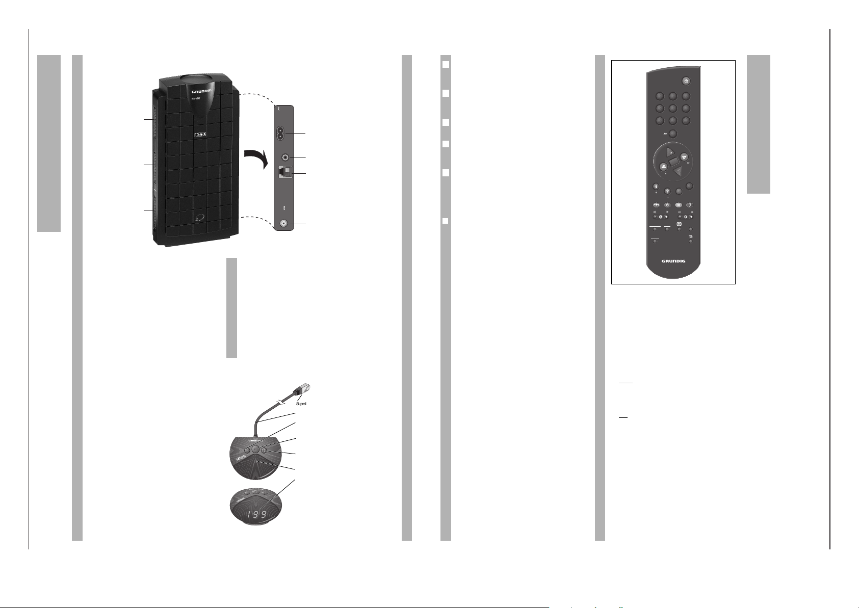
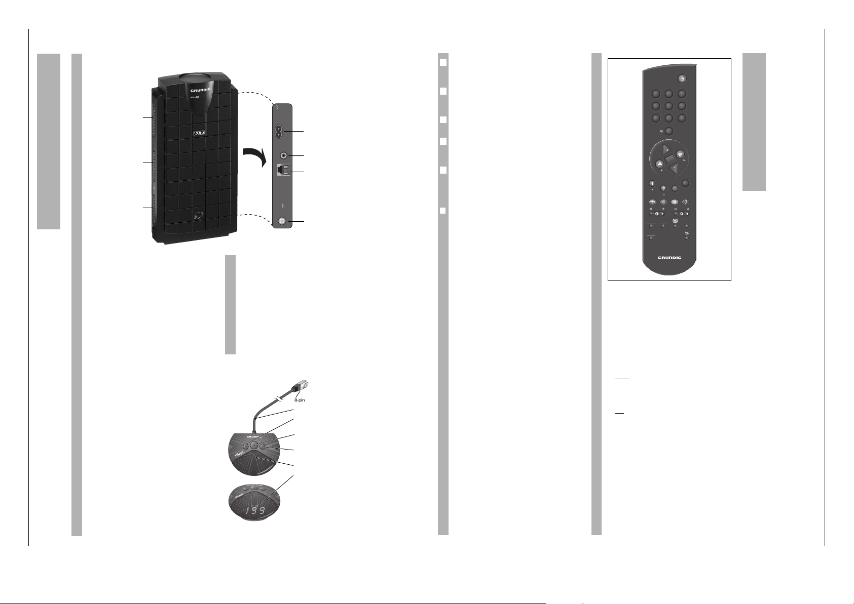
Der Receiver auf einen Blick
R
SAT
Mouse
950-2150MHz
14/19V
0.3A max.
REMOTE
Control
VCR
INPUT-SAT
220-240V
50-60Hz
Remote Control/VCR
Anschluß zur Fernbedienung durch GRUNDIG
Videorecorder (siehe Kapitel “Videoaufzeichnungen
und Timermenü” auf Seite 19) und für Datalink
(siehe Kapitel “Sonderfunktionen” auf Seite 20).
Bei Befehlen über diese Buchse erscheint »rC« in
der Anzeige der SAT-Mouse.
Anschluß für Netzkabel
Remote Control/VCR
SAT-Mouse
SAT-Antenne
SCART-
EURO-AV-
Anschlüsse
TV
DECODER
VCR
1 9 9
8-poliger Western-Stecker
Anschlußkabel
Programmplätze abwärts schalten/
einschalten aus Bereitschaft.
Gerät in Bereitschaft (Stand-by)
schalten.
Programmplätze aufwärts schalten/
einschalten aus Bereitschaft.
Infrarotempfänger
Programmplatzanzeige/ bei Bereit-
schaft Anzeige »-«
Mit der Universalfernbedienung TP 820 SAT lassen
sich alle Tastenfunktionen und Grundeinstellungen
durchführen.
Die Fernbedienung kann auch TV-Geräte von
GRUNDIG und einigen anderen Herstellern bedienen (siehe Kapitel “Universalfernbedienung”).
Einige Tasten der Fernbedienung haben spezielle
Funktionen im Menü (siehe Seite 11).
Bitte beiliegende Batterien einsetzen und Polung
beachten! Markierung hierfür im Fachboden. Deckel
schließen.
Wechseln Sie bitte die verbrauchte Batterien rechtzeitig. Die Bildschirmeinblendung »Batterie Telepilot« fordert Sie dazu auf. Für Schäden, die durch
ausgelaufene Batterien entstehen, kann nicht gehaftet werden.
❒
Tastenfunktionen
b
Gerät in Bereitschaft (Stand-by) schalten.
0…9 Mit den Zifferntasten wird der entspre-
chende Programmplatz direkt angewählt, z.B. P 123.
Bei mehrstelliger Programmplatzwahl
werden die Ziffern in der Reihenfolge
von links nach rechts eingegeben. Im
Beispiel also 1, 2 und 3 eintippen.
So können Sie insgesamt bis zu 199
SAT-Programmplätze (SAT-TV und
SAT-Radio) anwählen.
– Einschalten des Receivers aus Bereit-
schaft (Stand-by).
Programmplatz schrittweise weiterschalten (länger drücken: Schnelldurchgang) sowie einschalten aus Bereitschaft auf den zuletzt eingestellten Programmplatz (Last Station Memory).
O Anzeige des Sendernamens auf dem
Bildschirm;
im Menü: speichern
– Im SAT-Mode: Lautstärke ändern (bei
sehr geringer Lautstärke erscheint auf
dem Bildschirm »SAT Mute«.
.
MENUE Aufrufen der Menütafeln
¢
D
Ohne Funktion
¢
TXT
EXIT Menütafel verlassen (ohne speichern)
¢
A/B
TV-GUIDE Ohne Funktion
k
(rot) Buchsenumschaltung. (siehe Kapitel
“Der STR 110 … als Zweitreceiver” auf
Seite 21)
h
(grün)Timermenü aufrufen.
j
(gelb) Umschalten zwischen Stereo, rechtem
und linkem Tonkanal.
5
4
3
2
1
g
RADIO Umschalten zwischen SAT-TV- und
(blau) SAT-Radio-Betrieb.
™ – Im TV-Mode*: Kontrasteinstellung des
TV-Gerätes ändern.
® – Im SAT-Mode: Aufrufen des Menüs zur
Bild- und Tonverbesserung (siehe Kapitel “Betrieb”).
– Im TV-Mode*: Helligkeitseinstellung
des TV-Gerätes ändern.
¢
SAT 1/TV TV-Mode*:
Bedienen eines TV-Gerätes durch
gleichzeitiges Drücken dieser Taste und
der gewünschten Funktionstaste *.
¢
SAT 2 Bedienen eines zweiten SAT-Receivers
(IR-Ebene 2) durch gleichzeitiges
Drücken dieser Taste und der
gewünschten Funktionstaste*.
¢
C
Ohne Funktion.
¢
PERI Manche TV-Geräte schalten bei Inbe-
triebnahme des SAT-Receivers automatisch vom terrestrischen Betrieb in
den AV-Betrieb.
Mit der Taste
¢
PERI kann in den terre-
strischen Betrieb des TV-Gerätes
zurückgeschaltet werden.
* Siehe auch Kapitel Universalfernbedienung
Die Fernbedienung
]
x
“
c
|
]
¢
“
¢
|
TV
DEC
VC
321
654
987
0
P
OK
P
MENUE
SAT 1/TV SAT 2 PERI
VIDEO
TV-GUIDE
EXIT
A/B
TXT
RADIO
DX
TP 820 SAT
Page 7
GRUNDIG Service 1 - 7
STR 110 micrSAT Allgemeiner Teil / General Section
Schaltsignal an der TV-Buchse
e
Modus : single
Diese Funktion legt fest ob bzw. wann eine Schaltspannung an der EURO AV Buchse TV ausgegeben
wird. Sie können zwischen den folgenden Einstellungen wählen:
single Dies ist die Grundeinstellung. Bei einge-
schaltetem Receiver gibt dieser an der
Buchse TV eine Schaltspannung aus. Viele
TV-Geräte schalten dadurch automatisch in
den AV-Betrieb, d.h. das TV-Gerät zeigt das
Bild des SAT-Receivers.
twin Diese Einstellung wird nur benötigt, wenn
Sie den STR 110 micro SAT als Zweitreceiver an eine bestehende SAT-Anlage
anschließen wollen (siehe Seiten 21 … 23).
Um die Einstellung zu ändern, drücken Sie in der
Zeile »LNB LO« des Hauptmenüs die Taste
.
MENUE.
In der Menüzeile »Modus ...« können Sie die Einstellung mit den Tasten xcändern.
2
1
6
LNB LO 1 : 09750 pos
LNB LO 2 : 09750 pos
LNB LO 3 : 10000 pos
LNB LO 4 : 11475 pos
LNB Power : 14/18 Volt
e
Modus : single
Volume : 26
STORE = OK EXIT = TXT
❒
Lautstärke
e
Volume : 26
Mit dieser Funktion können Sie die Lautstärke der
SAT-Programme an die der terrestrischen Programme angleichen.
Um die Einstellung zu ändern, drücken Sie in der
Zeile »LNB LO« des Hauptmenüs die Taste
.
MENUE.
Die oben gezeigte Menüzeile erscheint und kann
dort mit den Tasten xcgeändert werden.
Geringere Werte als 10 werden nicht gespeichert.
6
1
6
Das Menü
❒
Decodereinstellung
e
Decoder : Auto
Wählen Sie im Hauptmenü mit den Tasten xcdie
gewünschte Einstellung.
Folgende Decodereinstellungen sind möglich:
Auto sollten Sie bei Decodern mit Schaltspannungs-
ausgabe einstellen (z.B. Première), der Decoder
schaltet sich automatisch in den Signalweg.
On sollten Sie bei Decodern ohne Schaltspannungs-
ausgabe wählen.
Mit der Taste
.
MENUE gelangen Sie in ein Untermenü für
weitere Decodereinstellungen.
In der Zeile »Norm« können Sie das Videosignal für den
Decoder zwischen FBAS, Basisband PAL (Deemphasis)
und Basisband linear umschalten. Bestimmte Decoder
benötigen diese Signaleinstellungen zur Einwandfreien
Decodierung.
In der Zeile »Mode« kann wie im Hauptmenü zwischen
»Auto« und »On« umgeschaltet werden.
In der Zeile »Signal « können Sie wählen, ob nur das
Videosignal oder das Audio- und das Video-Signal decodiert werden sollen.
5
4
3
2
6
1
Decoder
e
Norm : FBAS
Mode : Auto
Signal : Audio + Video
STORE = OK EXIT = TXT
LNB LO 1 : 09750 pos
LNB LO 2 : 09750 pos
LNB LO 3 : 10000 pos
LNB LO 4 : 11475 pos
LNB Power : 14/18 Volt
Modus : single
e
Volume : 26
STORE = OK EXIT = TXT
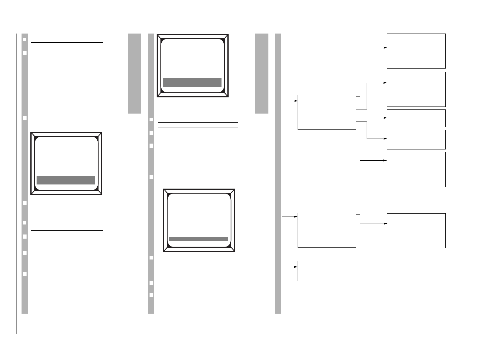
Hauptmenü
Timermenü
Menü zur Bild- und Tonverbesserung (Threshold/DX)
Menü-Übersicht
Programm : 1 TV
Name : ARD_ _
e
Frequenz : 11494.0 MHZ
LNB LO : LO1 (9.750)
Pol./Ant : H / 0 kHz A
Kontrast : 3 (37)
Decoder : Auto
Audio : 1 (7.02 ST)
P 199 Radio :
e
P 1 TV : ARD
P 2 TV : ZDF
P 3 TV : RTL
P 4 TV : SAT 1
P 5 TV : N-TV
P 6 TV : 3SAT
P 7 TV : PRO 7
e
LO 1 : 09750 pos
LO 2 : 09750 pos
LO 3 : 100000 pos
LO 4 : 11475 pos
LNB Power : 14/18 Volt
Modus : single
Volume : 26
e
Kontrast 1 : 16
Kontrast 2 : 19
Kontrast 3 : 36
Kontrast 4 : 16
e
Audio : 1
e
Audio L : 7,02 MHz
Audio R : 7,20 MHz
Mode : Stereo
Deem : Panda
Audio BW : 110 kHz
e
Threshold : off
Audio BW : 110 kHz
e
Timer 1 : on
Programm : 125 N-TV
Date : 24.12.96
Start : 21:00
Stop : 22:15
e
Timer 1 : off
Timer 2 : off
Timer 3 : off
Timer 4 : off
Date : 24.12.96
Time : 18:46
.
MENUE
® DX
h
.
MENUE
.
MENUE
.
MENUE
.
MENUE
.
MENUE
Decoder
Norm : FBAS
Mode : Auto
Signal : Audio + Video
.
MENUE
Page 8
Allgemeiner Teil / General Section STR 110 micrSAT
1 - 8 GRUNDIG Service
Operating Hints Note: This chapter contains excerpts from the operating instructions. For further particulars please refer to the appropriate user instructions the part number of which is indicated in the
relevant spare parts list.
The SAT Receiver
The unit is only disconnected from the mains
when the 230 V plug is removed!
EURO-AV connectors
TV EURO-AV socket (output only) for TV set,
with RGB transfer from the decoder
socket.
DEC EURO-AV socket (input/output) for
PAL/MAC decoders or a second video
recorder.
VCR EURO-AV socket (input/output) for a video
recorder or further PAL decoder.
The SAT Mouse
The SAT mouse receives the infrared signals from
the remote control unit and sends commands to the
receiver via the cable. Therefore mount the SAT
mouse somewhere where there are no obstacles
between it and the remote control unit. Instead
of using the remote control unit, you can also
switch the programme positions with the SAT
mouse keys.
When switching on from stand-by, the receiver
switches to the last selected programme position
(Last Station Memory).
The Receiver at a Glance
R
SAT
Mouse
950-2150MHz
14/19V
0.3A max.
REMOTE
Control
VCR
INPUT-SAT
220-240V
50-60Hz
Remote control/VCR
Connector for remote control of the receiver via a
GRUNDIG video recorder (see chapter “Video
Recordings and Timer Menu” on page 19) and for
the Datalink function (see chapter “Special Functions” on page 20).
When commands are given via this connector, the
indication “rC” appears in the display of the SAT
mouse.
Mains cable connector
Remote control/VCR
SAT mouse
SAT aerial
SCART
EURO-AV
connections
TV
DECODER
VCR
1 9 9
8-pin Western plug
Connection cable
Switch programme position down-
wards / switch on from stand-by.
Switch receiver to stand-by.
Switch programme position
upwards / switch on from stand-by
Infrared receiver
Programme position indication /
”-” indication in stand-by
All operating functions and basic settings can be
carried out using the TP 820 SAT universal remote
control unit.
The remote control unit can also be used to control
TV sets from GRUNDIG and many other makes (see
chapter on “Universal Remote Control”).
Several keys on the remote control have special
functions in the menu (see page 11).
Please insert the batteries supplied observing correct polarity! Markings on the base of the compartment indicate this. Close cover.
Please change used batteries promptly. The onscreen display “Batterie Telepilot” signals when the
batteries must be changed. We can accept no
liability for damage caused by leaking batteries!
❒
Key Functions
b
Switch receiver to stand-by.
0…9 The required programme position is
selected directly by pressing the digit
keys, e.g. P 123.
When selecting a multi-digit programme position, the digits are
entered in order from left to right. So,
in the example, you would enter 1, 2
and 3.
In this way you can select up to 199
SAT programme positions (SAT TV
and SAT radio).
– Switch receiver on from stand-by.
Switch through programme positions
step by step and switch on from
stand-by to the last programme position selected (Last Station Memory).
O Display name of station on screen;
when in a menu: save.
– In SAT mode: alter volume (at very
low volume, “SAT Mute” is displayed
on the screen.
.
MENUE Display on-screen menu guide.
¢
D
Without function
¢
TXT
EXIT Exit menu (without saving).
¢
A/B
TV-GUIDE Without function
k
(red) Socket switching (see chapter
“The STR 110… as Second Receiver”,
page 21).
h
(green) Display Timer menu.
j
(yellow)Switch between stereo, right and left
sound channel.
5
4
3
2
1
g
RADIO Switch between SAT-TV and SAT
(blue) radio mode.
™ – In TV mode*: alter contrast setting of
TV set.
® – In SAT mode: display menu for picture
and sound improvements (see chapter
“Using the Receiver”).
– In TV mode*: alter brightness setting of
TV set.
¢
SAT 1/TV TV mode*.
Control a TV set by pressing this key
and the desired function key simultaneously*.
¢
SAT 2 Control a second SAT receiver
(IR level 2) by pressing this key and the
desired function key simultaneously*.
¢
C
Without function.
¢
PERI Certain TV sets switch automatically
from terrestrial mode to AV mode
when the SAT receiver is switched on.
The
¢
PER key can be used to switch
the TV set back to terrestrial mode.
* See also chapter “Universal Remote Control”.
The Remote Control
]
x
“
c
|
]
¢
“
¢
|
TV
DEC
VC
321
654
987
0
P
OK
P
MENUE
SAT 1/TV SAT 2 PERI
VIDEO
TV-GUIDE
EXIT
A/B
TXT
RADIO
DX
TP 820 SAT
Page 9

STR 110 micrSAT Allgemeiner Teil / General Section
GRUNDIG Service 1 - 9
❒
Switching voltage on TV socket
e
Modus : single
This option determines whether and when a switching voltage is available at the TV EURO AV
socket. You have the choice between the following
options:
single Basic setting. When the receiver is switched
on, a switching voltage is available at the TV
socket. Many TV sets then switch automatically in the AV mode and show the picture
from the SAT receiver on the picture screen.
twin This option must be selected if you wish to
connect the STR 110 micro SAT as second
receiver to an existing SAT system (see
pages 21 to 23).
To change the setting, press the
.
MENUE key when
in the “LNB LO” line of the main menu.
In the “Modus ...” menu line, you can change the
setting using the xckeys.
2
1
6
The On-Screen Menu Guide
LNB LO 1 : 09750 pos
LNB LO 2 : 09750 pos
LNB LO 3 : 10000 pos
LNB LO 4 : 11475 pos
LNB Power : 14/18 Volt
e
Modus : single
Volume : 26
STORE = OK EXIT = TXT
❒
Volume
e
Volume : 26
This function is used to adjust the volume of the
SAT programmes to the volume of the terrestrial
programmes.
To change the setting, press the
.
MENUE key when
in the “LNB LO” line of the main menu. The menu
line shown above is displayed and you can change
the setting using the xckeys.
Values below 10 are not saved.
6
1
6
LNB LO 1 : 09750 pos
LNB LO 2 : 09750 pos
LNB LO 3 : 10000 pos
LNB LO 4 : 11475 pos
LNB Power : 14/18 Volt
Modus : single
e
Volume : 26
STORE = OK EXIT = TXT
❒
Decoder settings
e
Decoder : Auto
Use the xckeys to select the desired setting in
the main menu.
The following decoder settings are possible:
Auto Select this option for decoders which sup-
ply a switching voltage (e.g. Première);
the decoder then is automatically
switched into the signal path.
On Select this option for decoders without
switching voltage generation.
Press the
.
MENUE key to display the decoder
settings menu.
In the “Norm” menu line, you can switch the video
signal for the decoder between FBAS, Baseband,
PAL (deemphasis) and linear Baseband. Certain
decoders require these signal settings for correct
operation.
In the “Mode” menu line, you can switch between
“Auto” and “On” (like in the main menu).
In the “Signal” menu line, you can select whether
only the video signal or the video and the audio
signal is to be decoded.
5
4
3
2
6
1
Decoder
e
Norm : FBAS
Mode : Auto
Signal : Audio + Video
STORE = OK EXIT = TXT
Main menu
Timer menu
Menu for picture and sound improvement (Threshold/DX)
Menu Overview
Programm : 1 TV
Name : ARD_ _
e
Frequenz : 11494.0 MHZ
LNB LO : LO1 (9.750)
Pol./Ant : H / 0 kHz A
Kontrast : 3 (37)
Decoder : Auto
Audio : 1 (7.02 ST)
P 199 Radio :
e
P 1 TV : ARD
P 2 TV : ZDF
P 3 TV : RTL
P 4 TV : SAT 1
P 5 TV : N-TV
P 6 TV : 3SAT
P 7 TV : PRO 7
e
LO 1 : 09750 pos
LO 2 : 09750 pos
LO 3 : 100000 pos
LO 4 : 11475 pos
LNB Power : 14/18 Volt
Modus : single
Volume : 26
e
Kontrast 1 : 16
Kontrast 2 : 19
Kontrast 3 : 36
Kontrast 4 : 16
e
Audio : 1
e
Audio L : 7,02 MHz
Audio R : 7,20 MHz
Mode : Stereo
Deem : Panda
Audio BW : 110 kHz
e
Threshold : off
Audio BW : 110 kHz
e
Timer 1 : on
Programm : 125 N-TV
Date : 24.12.96
Start : 21:00
Stop : 22:15
e
Timer 1 : off
Timer 2 : off
Timer 3 : off
Timer 4 : off
Date : 24.12.96
Time : 18:46
.
MENUE
® DX
h
.
MENUE
.
MENUE
.
MENUE
.
MENUE
.
MENUE
Decoder
Norm : FBAS
Mode : Auto
Signal : Audio + Video
.
MENUE
Page 10

Allgemeiner Teil / General Section STR 110 microSAT
Service- und Sonderfunktionen
1. Infrarot-Ebene umstellen (z.B. bei zwei SAT-Receiver)
- Linke Taste (Minustaste) der SAT-Maus gedrückt halten und Netzspannung an den Receiver anschließen. Am Bildschirm und in der
7-Segmentanzeige der SAT-Maus erscheint die jeweils eingestellte
Anzeige "IR 1" oder "IR 2".
- Über das Bildschirm-Menü mit den Fernbedientasten 3 4 die Infrarot-Ebene IR 1 oder IR 2 auswählen.
- Mit "OK" speichern.
2. Data Link Übertragung
Zur gleichen Senderprogrammierung mehrerer STR 110.
Mit einem Cinch-Kabel an der Remote-Buchse beide Geräte verbinden.
- Rechte Taste (Plustaste) der SAT-Maus gedrückt halten und Netzspannung an den Receiver anschließen.
Am Bildschirm und der 7-Segmentanzeige der SAT-Maus erscheint
die Anzeige "SE" (send).
Während der Übertragung der Programmdaten erscheint am Bildschirm des Master-Receivers "Senden", auf der 7-Segmentanzeige
der SAT-Maus "SE".
Am Bildschirm des Slave-Gerätes erscheint bei der Übertragung
"Empfangen", auf der 7-Segmentanzeige der SAT-Maus "rC".
Nach fehlerfreier Programmierung schalten beide Receiver in den
Programm-Mode.
Ist die Übertragung fehlerhaft, erscheint am Bildschirm die Anzeige
"Fehler" und auf der SAT-Maus "Er". Vorgang wiederholen.
3. Programmdaten mit PC einspielen
Zur individuellen Veränderung der Programmdaten.
- Interface an die Buchse der SAT-Maus anschließen.
Dadurch wird der I2C-Bus des Receivers nur noch vom PC-Programm gesteuert.
- Gewünschte Programmbelegung einspielen.
Service and Special Functions
1.Changing the Infrared Level (e.g. for two SAT Receivers)
- Depress and hold the left button (minus) on the SAT mouse and
connect the receiver to the mains. The actual setting "IR 1" or "IR 2"
is indicated on the screen and on the 7-segment displayof the SAT
mouse.
- Select the infrared level IR 1 or IR 2 on the menu displayed on the
screen using the remote control buttons 3 4.
- Store with "OK".
2. Data Link Transfer
For setting the channels on several STR 110 receivers at the same
time.
Connect both receivers with a Cinch cable on the remote socket.
- Depress and hold the right button (plus) on the SAT mouse and
connect the receiver to the mains.
The indication "SE" (send) appears on the screen and on the 7segment display of the SAT mouse.
During the programme data is transferred, the message "Senden"
(send) is displayed on the screen of the Master receiver, and "SE"
is shown on the 7-segment display of the SAT mouse.
On the Slave receiver, the display shows "Empfangen" (receive)
during data transfer, and "rC" is indicated on the 7-segment display
of the SAT mouse.
On successful completion of the programming both receivers switch
to programme mode.
If the data transfer was not successful, the indication "Fehler" (error)
appears on the display, and the SAT mouse shows "Er". Repeat.
3. Entering the Programme Data via a PC
For changing the programme data individually.
- Connect the interface with the socket of the SAT mouse.
Consequently, the I2C-bus of the receiver will only be driven by the
PC programme.
- Enter the desired programmes.
GRUNDIG Service1 - 10
Page 11

STR 110 microSAT Schaltungsbeschreibung / Circuit Description
1.3 Regelung
D
Schaltungsbeschreibung
Steigt die Belastung im Trafo, sinken alle Spannungen und damit auch
die Spannung an Pin 2 des OK1736 über den Regelverstärker TL 431
und die Diode D1736. Die Spannung am Gate des TL431 ist typ. 2,5V.
1. Netzteil
1.1 Allgemein
Die Generation des TOPSwitch-Sperrwandlernetzteils zeichnet sich
durch nur geringe Außenbeschaltung des PowerMOSFET-IC1725 und
einer festen Schaltfrequenz von 100kHz aus. Die Regelung und Fehlererkennung wird ausschließlich über eine Impulsbreitenmodulation (PWM)
vorgenommen.
Anschlüsse des IC1725
Drain Pin:
Drain-Ausgang des internen MOSFET-Transistors T1. Er liefert den
Startstrom für die Anlaufphase über einen eingebauten Hochvoltschalter und mißt den Strom über ZC.
Control Pin:
Fehlererkennung und Regelungseingang für den internen Shuntregler
im Normalbetrieb. Außerdem Triggereingang für Schutzschaltung und
Wiederanlauf nach automatischer Abschaltung.
Source Pin:
Source-Ausgang des internen MOSFET-Transistors T1. Primärmasse
des Netzteils und Bezugspunkt.
1.2 Funktion
Die Stromversorgung für das Drain des IC1725 liefert der Gleichrichter
D1712 über die Wicklung 5, 4 des Sperrwandlertrafos. Am Ladeelko
C1717 steht bei 230V Netzspannung ca. 320V.
Nach Anliegen der Betriebsspannung schwingt der interne Oszillator
an. Während der Leitphase des ICs wird Energie im Übertrager
gespeichert und während der Sperrphase über die Sekundärwicklung
abgegeben. Um die Sekundärspannungen stabil zu halten, wird der
Control-Eingang des IC1725 (typ. 5,7V) mit einer Referenzspannung
über den Optokoppler OK1736 geregelt.
Dadurch leuchtet die LED im Optokoppler dunkler. Der Transistor
zwischen Pin 4 und Pin 5 wird hochohmiger. Die Spannung wird kleiner
im Verhältnis zur Sägezahnspannung an Pin 2 und damit wird die
Leitzeit des Hochvolttransistors T1 im IC1725 länger. Somit regelt die
Spannung hoch.
Liegt auf der Sekundärseite ein Kurzschluß vor, steigt der Strom durch
den MOSFET an und die eingebaute Schutzschaltung taktet das
Netzteil im Rhythmus von 1-2 Sekunden. Entfällt die Belastung,
schaltet die Auto-Restartstufe im IC erneut selbsttätig das Netzteil ein.
Die Dioden D1723, D1722 begrenzen die Spannungsspitzen der
Überschwinger am Drainausgang des IC1725.
1.4 Sekundärspannungen
+33V: Abstimmspannung für den SAT-Tuner über Diode D1731.
+19V: LNC-Versorgungsspannung über die Diode CD1732.
+14V: LNC-Versorgungsspannung über die Diode CD1733.
+12V: Versorgungsspannung über Diode CD1735 für die Signal-
verarbeitung.
+5V/D: Versorgungsspannung über CD1736 für den µP CIC1400,
SAT-Tuner und OSD-Prozessor IC1330.
1.5 LNC-Spannungsversorgung
Durch die getrennte 14/18V Spannungsversorgung LNC Power wird
die Leistungsaufnahme reduziert. Wird für das LNC 14V angefordert,
öffnet der Befehl U
Schalter CT1732 sperrt die Spannung 19V an CD1732. Bei 18V "LNC
den Transistor CT1746 und der MOSFET-
14/18V
Power" sperrt CT1746 und CT1732 öffnet.
Der Strombegrenzungswiderstand CR1760, IC1760-(2) ist so dimensioniert, daß der Low-Drop-Regler IC1760 die "LNC Power" abschaltet
falls der LNC-Strom 350mA überschreitet. Die Leitung LNC_PG leitet
die Überstrommeldung an den µP CIC1400-(60) und schaltet über den
Befehl U
ab. Am Bildschirm erscheint dazu die Meldung "LNC ?".
die "LNC Power" im Abfragetakt von ca. 4-5 Sekunden
LNC OFF
1.6 Standby-Betrieb
Pin Belegung IC1725
DRAIN
SOURCE (TAB)
CONTROL
TOP201
Im Standby-Betrieb schalten die MOSFET-Schalter CT1733 die Verbraucher +12V und +5V mit der Schaltspannung U
CT1736 ab und reduzieren damit die Stromaufnahme.
über CT1737,
Standby
Blockschaltbild IC1725
Control
Z
Shunt Regulator/
T2
R
C
Error Amplifier
I
FB
Oscillator
D
Max
Clock
SAW
E
V
C
Shutdown/
Auto-Restart
Externally
Triggered
Shutdown
Thermal
Shutdown
-
+
PWM
Comparator
+
-
-
+
5.7V
5.7V
4.7V
Power-up
Reset
0
Internal
Supply
1
8
+
V
-
I
Minimum
On-Time
Delay
Limit
S
Q
RQ
S
RQ
Controlled Turn-on
Gate Driver
Q
Leading
Edge
Blanking
Drain
T1
Source
GRUNDIG Service 2 - 1
Page 12

Schaltungsbeschreibung / Circuit Description STR 110 microSAT
2. Systemsteuerung
Dieses System enthält den maskenprogrammierten Mikrocomputer
(CIC1400) und den EPROM CIC1420 als NVM für die Programmdaten
wie Frequenztabelle, Senderkennung, HUB usw. Der Datenverkehr
zwischen dem µP und IC1100, IC1330 und dem SAT-Tuner findet über
den I2C-Bus statt.
2.1 Pin-Belegung des Prozessors CIC1400
Pin 30:
Einschaltreset des Prozessors, erzeugt von IC1402. Erst wenn alle
Versorgungsspannungen des Empfängers aufgebaut sind, beginnt
der Programmablauf.
Pin 28, 29:
Der Systemtakt wird von einem Oszillator erzeugt dessen Frequenz
durch Q1402 (4MHz) bestimmt wird. Ein Teil dieses Signals wird als
Taktsignal dem IC1100 über CC1025 und CR1025 zugeführt.
Pin 59:
Der IR-Eingang ist LOW-aktiv.
Pin 60:
LNC_PG (Power Good) dient zur Erkennung eines Kurzschlusses am
LNC-Anschluß. Bei einem LNC-Strom < 350mA wird über U
IC1760 die Spannung LNC Power abgeschaltet.
Pin 61:
Datenausgang für die Remote Cinchbuchse, z. B. zur Data LinkÜbertragung.
Pin 62:
VDR-Ausgang für die Anzeige in der SAT-Mouse.
Pin 63:
Schaltet die 22kHz-Frequenz, IC1100-(29), auf die Spannung "LNCPower" zur Steuerung der LNCs. Dieses 22KHz-Ausgangssignal
kann, je nach Wahl, auch mit einem DiSEqC-Protokoll impulsmoduliert sein.
Pin 64:
Schaltspannung U
oder vertikal von spannungsgesteuerten Polarotoren; "High" = hori-
zur Wahl der Polarisationsebene horizontal
14/18V
zontale Ebene.
Pin1:
Schaltspannung U
Pin 2:
Schaltspannung U
+12V und +5V.
zur Abschaltung der LNC-Versorgungsspannung.
LNC OFF
zur Abschaltung der Versorgungsspannungen
Standby
Pin 13:
Dateneingang von der Remote Cinchbuchse, zur Fernsteuerung (z. B.
Timerbetrieb) durch einen Videorecorder.
Pin14:
Anschluß zur Nahbedientaste "TASTER UP" in der SAT-Mouse.
Pin 19:
Abfrage, ob die Synchronsignal-Detektorschaltung IC1330 einen Sync.
ausgibt. Bei zu kleinem oder schlechtem Signal schaltet der µP auf
interne Synchronisation und der Bildschirmhintergrund wird blau. Mit
der Fernbedientaste "grün" können Sie den Bildschirmhintergrund
zwangsweise grün schalten.
Pin 21:
AV-Schaltspannungseingang zur Auswertung der Schaltspannung an
Pin 8 der Decoder-Buchse. Bei High-Pegel "AV IN1" wird das Videosignal über den angeschlossenen Descrambler zum Receiver zurückgeführt.
Pin 22:
AV-Schaltspannungseingang zur Auswertung der Schaltspannung an
Pin 8 der VCR-Buchse. Bei High-Pegel "AV IN 2" wird das VCR-Signal
zum TV-Gerät durchgeschleift (Matrix).
Pin 23:
Anschluß zur Nahbedientaste "DOWN" in der SAT-Mouse.
Pin 24:
Regelspannung U
Pin 48, 49:
zur Frequenznachregelung des SAT Tuners.
AFC
System-Daten und -Clockleitung zur Steuerung des Tuners, IC1100,
IC1330, CIC1420 (I2C-Bus).
Pin 37:
Freigabesignal CS
Pin 38:
(Chip Select OSD) für den OSD-Controller IC1330.
OSD
RGB/TV-Schaltspannung zur Umschaltung der Scartbuchsen (Matrix). Bei RGB/TV-Schaltspannung "High" schalten CT1270, CT1226
das FS-Gerät auf RGB-Betrieb.
Pin 39:
AV 3-Schaltspannungserzeugung für Pin 8 der TV-Buchse.
Pin 40/41:
Serielle Clock- und Datenleitung zur Steuerung des Uhren-CIC1120.
LNC OFF
und
2.2 Nichtflüchtiger Speicher
Der NVM CIC1420 ist ein serieller EEPROM, in dem alle werkseitig
programmierten oder kundenspezifischen Daten zur Konfiguration
des Empfängers gespeichert sind (Frequenztabelle, Hub, Polarisation
usw.).
2.3 Clock-IC CIC1120
Der Clock-IC1120 schwingt mit einer Taktfrequenz von 32,768kHz, die
der Quarz Q1121 steuert. Bei Stromausfall hat die Lithium-Batterie
eine Gangreserve von ca. 6-7 Jahren.
3. Tuner
Der CIC 1400 steuert über den I2C-Bus alle Tunerfunktion.
Vom LNC gelangen die ZF-Signale mit einem Frequenzbereich von
900MHz bis 2150MHz an den Antennen-Eingang.
Der LNC-Eingang ist wechselspannungsmäßig mit einem regelbaren
Verstärker gekoppelt. Die Verstärkung regelt die AGC automatisch,
um den Pegel am Eingang des FM-Demodulators konstant zu halten.
Am Ausgang, Kontakt 4 des Tuners steht das Basisbandsignal zusammen mit dem 25Hz Verwischungssignal.
Zur Verbesserung des Bildes kann für verrauschte Sendersignale
über das Menü im Tuner eine "Treshold"-Schaltung aktiviert werden.
4. Audiosignalweg
Anmerkung zum Blockschaltbild:
zwei Schaltkreise des IC's, ein Schaltkreis für jeden Stereokanal. Die
erste Zahl bezieht sich auf den rechten Kanal.
IC1100 STV0056A
23
FM in
AGC
42,26
AMPLOCK
46,41
Blockschaltbild Audio-Demodulator
G1
Der FM-Audio-Demodulator ist PLL-gesteuert.
Der Bandpaß CC1014, L1014, CC1016, L1016, L1019, CC1017,
CR1017, L1017 befreit das FM-Signal des Basisbandes von unerwünschten Videosignalkomponenten.
Der Ansteuerpegel der zu demodulierenden Signale ist festgelegt,
damit die Ausgangsamplitude vom Demodulator gleich bleibt. Daher
durchläuft das Eingangssignal den Regelverstärker G1, dessen Verstärkung wird durch einen der beiden Pegeldetektoren eingestellt. Wird ein
Signal erstmals gewählt, erfaßt der Detektor 1 die kombinierte FMSignalamplitude und G1 stellt auf eine annähernd korrekte Verstärkung ein. Hat die PLL einmal die Verstärkung eingeregelt, überwacht
der Pegeldetektor 2 den tatsächlichen Signalpegel innerhalb der PLL.
Wird ein neuer Tonträger gewählt, muß die PLL auf die neue Frequenz
abgestimmt werden. Dazu wird S1 geschlossen und der spannungsgesteuerte Oszillator (VCO) wird mit dem Frequenz-Synthesizer eingeregelt. Ein Frequenzzähler mißt die VCO-Frequenz. Ist der VCO auf
die Frequenz abgestimmt, öffnet S1 und der VCO rastet auf den
eingespeisten Tonträger der gleichen Frequenz ein. Im Rückkopplungssignal des Regelkreises am Eingang von G2 ist die FM-Modulation enthalten. Die Verstärkung von G2 kann für verschiedene FMHübe nachgeregelt werden. Das PLL-Filter sorgt für die notwendige
Stabilität des Regelkreises.
Sämtliche Funktionen im Demodulator werden über den I2C-Bus
(SDA, SCL) von CIC1400 gesteuert.
Zwei Zahlen an einem Pin stehen für
Level
Detector 1
Level
Detector 2
PLL
Filter
47,39
Frequen cy
I2C Bus
Counter
SDA
{
SCL
G2
V/I
90
VCO
0
Frequen cy
Synt hesizer
30
31
To Audio
Processing
S1
C-PU MP
49,38
2 - 2 GRUNDIG Service
Page 13

STR 110 microSAT Schaltungsbeschreibung / Circuit Description
Anmerkung:
Zwei Zahlen an einem Pin stehen für zwei Schaltkreise
des IC's, ein Schaltkreis für jeden Stereokanal. Die erste Zahl bezieht
sich auf den rechten Kanal.
Blockschaltbild Audiosignalverarbeitung
r
o
From FM
Demodulat
S1
6dB
28,27 25,24
To DEC
SCART
6dB
-
From DEC SCART
IC1100
S2
STV 0056A
NRS
Peak
Detector
Band-Pass
Filter
S3
51,522,543,53 1,55
NRS Time
Cons tan t
NRS Filte r
Passive
A udi o
De-emphasi s
33,34 48,40 14 ,12 6,1022,21
De-emphasi s
J17
I2C Bus
De-emphasi s
SDA
{
SCL
75
u
S
S4
6dB
S5
To VCR SCART
-
6dB
30 31
S6
Vol
From
VCR SCART
To
TV SCAR T
4.1 Rauschunterdrückungssystem (Noise Reduction System NRS)
Das NRS (Rauschunterdückungssystem) umfaßt einen Spitzenpegeldetektor und einen geregelten Tiefpaß. Das Audiosignal des jeweiligen Kanals wird dem Spitzenpegeldetektor zugeführt, einem externen
Bandpaßfilter begrenzt und von den Transistoren CT1073, CT1081
gemittelt.
Die Ausgangsspannung des jeweiligen Spitzendetektors wird gespeichert in der NRS-Zeitkonstante. Dieser ist ein Gleichspannungspegel,
der sich mit der Amplitude des Audiokanal-Signals ändert und zur
Regelung des Frequenzgangs des NRS-Filters über einen regelbaren
kapazitiv behafteten Verstärker verwendet wird.
Schalter S3 schaltet das NRS-System ein.
4.2 Passive Deemphasis
S4 wählt die passive Deemphasis für den jeweiligen Audiokanal aus.
Mögliche Deemphasen sind J17 und 75µS, die mit externen Schaltkreisen eingestellt werden. Für die Deemphasis 50µS wird ein zusätzlicher interner Widerstand parallel zum 75µS-Schaltkreis geschaltet.
Bei dem PANDA-Verfahren arbeitet das NRS-System zusammen mit
der 75mµS-Deemphasis.
5. Video-Rauschfilter
In einem 10MHz-Tiefpassfilter wird das Basisband-Videosignal des Tuners
von unerwünschten Rauschsignalen befreit und zur weiteren Verarbeitung
dem Video-Prozessor und Audio-Demodulator, IC1100 zugeführt.
6. Videosignalverarbeitung
6.1 Video-Verstärkungsregelung im IC1100
Das Basisband-Videosignal vom Tuner wird wechselspannungsmäßig
an einem Regelverstärker eingekoppelt, dessen Verstärkung entsprechend der gewünschten Videoamplitude geregelt werden kann.
6.2 Video-Inverter
Bei manchen Sendern ist es notwendig, die Polarität des Videosignals
mit einem Schalter zu invertieren, z.B. für C-Band-Empfang.
Nach dem Invert-Wahlschalter wird es als Basisband-Eingangssignal
an die Videomatrix geführt.
6.3 PAL-Deemphasis
Das Basisband wird dem nicht-invertierenden Eingang eines Verstärkers mit einer in der Rückkopplungsschleife integrierten PAL-Preemphasis zugeleitet. Am Ausgang dieses Verstärkers steht ein PALrückentzerrtes Signal, das zur Pegelanpassung um 6dB bedämpft wird
und als PAL-Eingangssignal an die Videobuchsen (Matrix) gelangt.
Nach der Entzerrung wird das PAL-Signal in ein Tiefpassfilter eingespeist, in dem Frequenzen über 5MHz herausgesiebt werden. Anschließend gleicht eine Laufzeitentzerrungsschaltung die im Filter
entstandenen Verzerrungen wieder aus. Um das 25Hz-Dreiecksverwischungssignal abzutrennen wird es wechselstrommäßig an eine
Klemmschaltung gekoppelt. Als resultierendes Signal entsteht das
normale Videoeingangssignal für die Videomatrix.
15
PAL
NORMAL
VCR
TV
r
I2C Bus
SCL
30 31
Video Matrix
7 8
OSD_CS
OSD_SCK
OSD_SDA
OSD_RESET
OSD Bus from
CIC1400
Group
Delay
Corrector
IC1100 STV0056A
Baseband Video
From Tuner
From
Decod
From VCR SCART
From VCR SCART
To CIC1400
er
NO_SYNC
{
PK_SYNC
Video Gain
20
Clamp
13
Clamp
5
11
Clamp
Clamp
4
Syn c Detector
Blockschaltbild Video-Verabeitung
Low Pass
Filte r
-1
Sync Separator
To VCR
To TV SCART
Invert
Pre-emphasis
18
PAL
-
+
Black Le ve l
To
Decod e
SCART
-6dB
BASEBAND
DECODER
Adjust
On Scre en
Display
6.4 Audio-Video Matrix IC1100
Die Videomatrix ist eine Kreuzschiene, die jede beliebige Videoquelle
an jeden beliebigen der drei Ausgänge schalten kann. Außer den drei
oben genannten Quellen liegen auch die Videoeingangssignale von
den Buchsen TV , VCR und DEC an der Matrix, wobei jedes Signal auf
den gleichen Pegel geklemmt wird, um Schaltstörungen zu vermeiden. Wie die Videomatrix steuert der I2C-Bus auch die Inverterstufe
und die Videoverstärkung. Das Ausgangssignal der Matrix wird an die
TV, VCR- und DEC-Buchse geleitet.
Über Kontakt 10 der SCART-Buchsen wird die Megalogic-Steuerung
erreicht.
Mit der roten Fernbedientaste können Sie die Videoebenen durchschalten.
6.4.1 TV-Buchse
"High"-Pegel der Schaltspannung U
CT1254, CT1250 die 12V Schaltspannung an die TV Scart-Buchse -
CIC1400-(39) schaltet über
AV OUT 3
Kontakt 8 und damit den FS-Empfänger in den AV-Mode.
Gleichzeitig steht das Audio- und Videosignal an der VCR-Buchse zur
Aufnahme an.
6.4.2 VCR-Buchse
Bei VCR-Wiedergabe legt die Schaltspannung der VCR-Buchse - Kontakt
8, U
CIC1400-(22) das Audio-Videosignal an die TV-Buchse.
AV IN 2
6.4.3 Decoder-Buchse
Bei Decoder-Betrieb legt die Schaltspannung der DEC-Buchse Kontakt 8, U
Videosignal an die TV-Buchse.
CIC1400-(21), I2C-Bus das entschlüsselte Audio-
AV IN 1
Bei RGB-Betrieb schaltet die RGB-Schaltspannung der DEC-BuchseKontakt 16 über CT1276 und die Schaltspannung U
(38), CT1270, CT1277 die 12V RGB-Schaltspannung an die TV-
RGB TV
CIC1400-
Buchse. Das FS-Gerät schaltet auf RGB-Betrieb.
7. OSD-Einblendung und Synchronisation
Das Videosignal V
Einblendstufe verwendet. Sie fügt Menüs und Statusinformationen in
das am Bildschirm gezeigte Videosignal ein. Die Synchronböden des
Videosignals V
geklemmt.
TV OUT
Ist ein normgerechtes Synchronsignal vorhanden teilt CI1330-(14)
dem CIC1400 über die Leitung "EXO SYNC." mit, daß ein gültiges
Synchronsignal anliegt.
Ist kein gültiges Synchronsignal vorhanden, erzeugt IC1330 ein eigenes Synchronsignal, so daß der Bildschirmhintergrund blau wird und
eine Bildschirmeinblendung noch möglich ist.
Die gesamte OSD-Steuerung erfolgt über die Leitungen SDA, SCL
und CS OSD.
wird auch als Speisesignal für die OSD-
TV OUT
werden mit CT1350 auf einen festgelegten Pegel
}
SCART
SDA
9
To
VCR
GRUNDIG Service 2 - 3
Page 14

Schaltungsbeschreibung / Circuit Description STR 110 microSAT
1.3 Control
GB
Circuit Descriptions
When the load connected to the transformer increases, all voltages
decrease and with them the voltage on pin 2 of OK1736 via the control
amplifier TL 431 and diode D1736. The voltage at the gate of TL431 is
1. Power Supply
1.1 General
The TOPSwitch family of the switched-mode power supply units
distinguishes itself by a minimum number of peripheral components
connected to the PowerMOSFET-IC1725 and a fixed switching frequency
of 100kHz. Control and error signal identification is exclusively effected
with a pulse width modulator (PWM).
IC1725 pin configuation
Drain Pin:
Drain output of the internal MOSFET transistor T1. Supplies the
internal current during the start-up phase via an integrated highvoltage switch and is the current sense point via ZC.
typically 2.5V so that less light is emitted from the LED in the optocoupler.
The transistor between pin 4 and pin 5 becomes high resistance. In
proportion to the sawtooth voltage on pin 2 the voltage decreases and
consequently the conducting phase of the high-voltage transistor in
IC1725 becomes longer. The voltage will increase.
With a short circuit in the secondary side, the current flowing through
the MOSFET rises and the built in protection circuit triggers the power
supply unit at a cycle of 1-2 seconds. When the load is removed, the
power supply is started automatically by the Auto-Restart stage in the
IC.
Diodes D1723, D1722 are provided to limit the voltage peaks of
overshoots at the Drain output of IC1725.
1.4 Secondary Voltages
+33V: tuning voltage for SAT Tuner via diode D1731.
Control Pin:
Error signal identification and control input for the internal shunt
regulator during normal operation. It is also the trigger input for the
protection and auto-restart stages.
Source Pin:
Source output of the internal MOSFET transistor T1. Primary-side
chassis return for the power supply unit and reference point.
1.2 Function
The supply voltage for the Drain of IC1725 is delivered by the rectifier
D1712 via winding 5, 4 of the converter transformer. The electrolytic
capacitor C1717 charges to about 320V from a 230V mains supply.
On application of the operating voltage the internal oscillator starts to
oscillate and feeds out positive pulses from the Drain Pin. During the
conducting phase of the IC, engery is stored in the transformer which
is fed to the secondary winding during the cut-off phase. To hold the
secondary voltages at a constant level, the Control input of IC1725
(typ. 5,7V) is controlled by means of a reference voltage via the
optocoupler OK1736.
+19V: LNC supply voltage via diode CD1732.
+14V: LNC supply voltage via diode CD1733.
+12V: supply voltge for signal processing, via diode CD1735.
+5V/D: supply voltage via diode CD1736, for µP CIC1400, SAT Tuner
and OSD processor IC1330.
1.5 LNC Supply
The separate 14/18V LNC Power supply allows to reduce power
consumption. If 14V supply is requested for the LNC, the transistor
CT1746 is activated by command U
CT1732 stops the 19V voltage via CD1732. For 18V "LNC Power",
and the MOSFET-switch
14/18V
CT1746 is switched off and CT1732 is activated.
The current limiting resistor CR1760, IC1760-(2) is so designed that
the Low-Drop control-IC1760 switches off "LNC Power" if the LNC-
current exceeds 350mA. The LNC_PG lead transfers this overload
message to µP CIC1400-(60) and switches off the "LNC Power" with
the command U
by the message "LNC ?" indicated on the screen.
at a scanning cycle of 4-5 seconds accompanied
LNC OFF
1.6 Stand by Mode
In Stand by mode, the MOSFET switches CT1733 turn off the +12V
Pin Configuration IC1725
and +5V loads with the switching voltage U
thus reducing the current consumption.
via CT1737, CT1736
Standby
TOP201
Block Diagram IC1725
Control
Z
Shunt Regulator/
T2
R
V
C
Error Amplifier
I
FB
Oscillator
D
Max
Clock
SAW
E
DRAIN
SOURCE (TAB)
CONTROL
C
-
+
5.7V
5.7V
4.7V
Externally
Triggered
Shutdown
Thermal
Shutdown
+
PWM
Comparator
Shutdown/
Auto-Restart
+
-
Power-up
Reset
0
Internal
Supply
1
8
+
V
-
I
Minimum
On-Time
Delay
Limit
S
Q
RQ
S
RQ
Controlled Turn-on
Gate Driver
Q
Leading
Edge
Blanking
Drain
T1
Source
2 - 4 GRUNDIG Service
Page 15

STR 110 microSAT Platinenabbildungen und Schaltpläne / Layout of the PCBs and Circuit Diagrams
PAL
Pre-emphasis
Low Pass
Filte r
Group
Delay
Corrector
Clamp
Clamp
Clamp
Clamp
PAL
BASEBAND
NORMAL
DECODER
VCR
TV
13
5
20
18
-
+
-1
11
4
7 8
9
Video Gain
Baseband Video
From Tuner
From
Decod
From VCR SCART
From VCR SCART
Black Le ve l
Adjust
To
Decode
r
On Scre en
Display
Sync Separator
Sync Detector
To
VCR
To TV SCART
To VCR
Invert
NO_SYNC
PK_SYNC
To CIC1400
{
-6dB
Video Matrix
15
30 31
SCL
SDA
I2C Bus
}
IC1100 STV0056A
OSD_CS
OSD_SCK
OSD_SDA
OSD_RESE
T
OSD Bus from
CIC1400
er
SCART
SCART
VCR SCART
SCART
Schaltungsbeschreibung / Circuit Description
STR 110 microSAT Platinenabbildungen und Schaltpläne / Layout of the PCBs and Circuit Diagrams
Schaltungsbeschreibung / Circuit Description
2. Microcomputer Operation
This system contains the mask-programmed microcomputer (CIC1400)
and the NVM-type EPROM CIC1420 for the programme data like
channel table, station ident, deviation, and so on. The exchange of data
between the µP and IC1100, IC1330, and the SAT Tuner is carried out
on the I2C-bus.
2.1 Pin Configuration of Processor CIC1400
Pin 30:
Power-on reset for the processor, generated by IC1402. The programme sequence will not start before all supplies of the receiver have
built up.
Pin 28, 29:
The system clock is generated by an oscillator whose frequency is
determined by Q1402 (4MHz). A proportion of this signal is fed through
CC1025 and CR1025 and is used to provide clock for IC1100.
Pin 59:
The IR input is active LOW.
Pin 60:
LNC_PG (Power Good) is used to detect the presence of a shortcircuit on the LNC. The LNC Power is switched off via U
IC1760 if the LNC current is < 350mA.
Pin 61:
Data output to the Remote Cinch socket, e. g. for data link transfer.
Pin 62:
VDR-output to the display on the SAT Mouse.
Pin 63:
Switches the 22kHz frequency ,IC1100-(29), to the "LNC Power"
supply to drive the LNC's. This 22kHz output signal can also be pulsemodulated with a DiSEqC protocol.
Pin 64:
Switching voltage U
voltage-controlled polarotors; "High" = horizontal.
Pin1:
Switching voltage U
Pin 2:
Switching voltage U
Pin 13:
Data input from the Remote Cinch socket for remote control (e. g.
Timer operation) by a video recorder.
Pin14:
Connection to local "TASTER UP" key in the SAT Mouse.
Pin 19:
Scans whether there is a sync signal fed out from the sync signal
detector circuit IC1330. If the signal is too low or poor the µP switches
to the internal synchronising signal and the screen background becomes blue. With the "green" key on the local keyboard it is possible
to change the background to green.
Pin 21:
AV switching voltage input for evaluation of the switching voltage on pin
8 of the decoder socket. If "AV IN1" is at high level the video signal is
fed back to the receiver via the connected descrambler.
Pin 22:
AV switching voltage input for evaluation of the switching voltage on pin
8 of the VCR socket. At high level "AV IN 2" the VCR signal is looped
through to the TV receiver (matrix).
Pin 23:
Connection to the local "DOWN" key in der SAT Mouse.
Pin 24:
Control voltage U
Pin 48, 49:
System data and clock lead to control the tuner, IC1100,IC1330,
CIC1420 (I2C-bus).
Pin 37:
Enable signal CS
Pin 38:
RGB/TV switching voltage for changing over the Scart sockets (matrix). When the RGB/TV switching voltage is at "High", CT1270,
CT1226 switch the TV receiver to RGB mode.
Pin 39:
AV 3 switching voltage to pin 8 of the TV-socket.
Pin 40/41:
Serial clock and data lead to drive clock CIC1120
GRUNDIG Service
to select horizontal or vertical polarity on
14/18V
to switch off the LNC supply.
LNC OFF
to switch off the +12V and +5V supplies.
Standby
for SAT Tuner frequency control.
AFC
(Chip Select OSD) for the OSD Controller IC1330.
OSD
2.2 Non Volatile Memory
Audio Processing Block Diagram
NVM CIC1420 is a serial EEPROM and contains all factory and user
I2C Bus
De-emphasi s
SDA
{
SCL
75
u
S
S4
6dB
S5
To VCR SCART
-
6dB
From
30 31
S6
Vol
To
TV SCAR T
LNC OFF
and
programmable data to configure the receiver (channel table, deviation,
polarity etc.).
2.3 Clock-IC CIC1120
Clock-IC1120 oscillates at a clock fequency of 32.768kHz under
control of quartz Q1121. In the case of a power failure a Lithium battery
is provided with a back-up capacity of approx. 6-7 years.
3. Tuner
All functions within the tuner are controlled from IC1400 via I2C Bus.
The IF signals from the LNC, in the range 900MHz to 2150MHz, are
supplied to the aerial input.
The LNC-input is AC-coupled into a variable amplifier whose gain is
adjusted automatically by the AGC to ensure a constant level at the
input to the FM Demodulator. At the output contact 4 of the tuner the
baseband signal is available together with the 25Hz energy dispersal
signal.
To improve the picture quality resulting from a noisy transmitter signal
a "threshold" circuit can be activated in the tuner via the menu.
r
o
From FM
Demodulat
S1
6dB
28,27 25,24
To DEC
6dB
-
From DEC SCART
IC1100
S2
STV 0056A
Peak
Detector
Band-Pass
Filter
NRS
S3
51,522,543,53 1,55
NRS Time
Cons tan t
Passive
A udi o
De-emphasi s
33,34 48,40 14 ,12 6,1022,21
NRS Filte r
De-emphasi s
J17
4. Audio Path
Note to the block circuit diagram
circuits exist, one for each stereo channel. The first number is for the
Right channel.
IC1100 STV0056A
23
FM in
AGC
AMPLOCK
42,26
46,41
G1
Audio Demodulator Block Diagram
The FM audio demodulator is of the Phase Locked Loop (PLL) type.
FM signals in the tuner Baseband Video signal are filtered by CC1014,
L1014, CC1016, L1016, L1019, CC1017, CR1017, L1017 which
removes unwanted Video components from FM in.
It is important that the drive level of the signals being demodulated is
fixed so that the output amplitude from the demodulator can be
predicted. To help achieve this the input signal passes through a gain
controlled amplifier G1, whose gain is set by one of two level detectors.
When a signal is first selected Level Detector 1, which senses the
combined FM signal amplitude, is used to set G1 to an approximately
correct gain. Once PLL lock has been reached Level Detector 2 is used
which accurately monitors the actual signal level within the working PLL.
When a new audio carrier is being selected the PLL must be tuned to the new
frequency. To do this S1 is closed and the Voltage Controlled Oscillator
(VCO) is adjusted by means of the Frequency Synthesiser. The VCO
frequency is read by the Frequency Counter. Once the VCO is on frequency
S1 is opened and the VCO locks onto the incoming carrier of the same
frequency. The control loop feedback signal at the input of G2 carries the FM
modulation. The gain of G2 can be controlled to handle different FM
deviations. Loop stability is maintained by the PLL filter.
Control of all functions in the Demodulator is via the I2C bus (SDA, SCL)
from IC1400.
Note:
Where two pin numbers are given two circuits exist, one for each
stereo channel. The first number is for the Right channel.
: Where two pin numbers are given two
Level
Detector 1
Level
Detector 2
PLL
Filter
47,39
Frequen cy
I2C Bus
Counter
SDA
{
SCL
30
G2
V/I
90
VCO
0
Frequen cy
Synt hesizer
31
To Audio
Processing
S1
49,38
C-PU MP
2 - 5
4.1 Noise Reduction System (NRS)
The NRS consists of a peak level detector and a controlled low pass
filter. Audio for each channel to its peak detector is band limited by an
external band-pass filter, and centred on the transistors CT1073,
CT1081.
The output of each peak detector is a voltage stored in its NRS time
constant. This is a dc level which will vary with the amplitude of the
audio channel signal and is used to control the frequency response of
its NRS filter via a variable transconductance amplifier.
Switch S3 is used to select the NRS system.
4.2 Passive Deemphasis
S4 is used to select the type of passive deemphasis that is applied to
each audio channel. The options are set by external networks and are
J17, and 75µS. 50µS is obtained by adding an internal resistor in
parallel with the 75µS network.
For PANDA operation NRS and 75µS are used together.
5. Video Noise Filter
Baseband video from the tuner is passed through a 10MHz low-pass
filer to remove unwanted noise before use by the Video Processor and
Audio Demodulator IC 1100.
6. Video Processing
6.1 Video Gain Control in IC1100
Baseband Video from the Tuner section is ac coupled into a controlled
amplifier whose gain can be set to give the desired Video amplitude.
6.2 Video Inverter
The polarity of the video signal can be set by the invert switch so that,
for instance, C band reception can be achieved.
After the invert selector switch this signal forms the baseband input to
the Video Matrix.
6.3 PAL Deemphasis
The baseband signal is applied to the non-inverting input of an
amplifier which has a PAL pre-emphasis network in its negative
feedback loop. The output of this amplifier is a PAL de-emphasised
signal which is attenuated by 6dB to make it level compatible, and
forms the PAL input to the Video sockets (matrix).
After the deemphasis the PAL signal is band limited by the 5MHz Lowpass Filter, followed by a Group Delay Corrector to compensate for
distortions in the filter and ac coupled into the clamp to remove the
25Hz energy dispersal waveform. This signal is the normal video input
to the Video Matrix.
GRUNDIG Service
Video Processing Block Diagram
6.4 Audio Video Matrix IC1100
This is a cross wire matrix of switches which can select any one of the
Video sources and make it available to each of the three outputs. In
addition to the three sources described above video is also fed to the
matrix from the TV , VCR and DEC sockets, each signal being clamped
to the same level to avoid switching disturbances. All Video Matrix,
Invert and Video Gain are controlled via I2C-bus. The output signal from
the matrix is sent to the TV, VCR and DEC socket.
Megalogic control is possible via contact 10 of the SCART sockets.
The video levels can be changed with the red key on the remote control
handset.
6.4.1 TV Socket
By a "High" level switching voltage U
switching voltage is fed through CT1254, CT1250 to the TV Scart
CIC1400-(39), the 12V
AV OUT 3
socket, contact 8, and consequently the TV receiver is switched to the
AV mode.
At the same time, the audio signal and video signal are provided on the
VCR socket for recording.
6.4.2 VCR Socket
On VCR playback the switching voltage from the VCR socket-contact 8,
U
CIC1400-(22) - applies the audio/video signal to the TV socket.
AV IN 2
6.4.3 Decoder Socket
On Decoder operation, the switching voltage from the DEC socket contact 8, U
video signal to the TV socket.
CIC1400-(21), I2C-bus - feeds the descrambled audio/
AV IN 1
On RGB operation, the RGB switching voltage from the DEC socket contact 16 via CT1276, and the switching voltage U
(38), CT1270, CT1277 - connects the 12V RGB switching voltage to
RGB TV
CIC1400-
the TV socket. The TV receiver changes to RGB mode.
7. OSD and Synchronisation
The video signal V
Display (OSD) insertion circuit which adds menus and status information to the video signal to be displayed on the TV. The sync tips of the
video signal V
The presence of a standard sync is signalled from CI1330-(14) to
TV OUT
CIC1400 via the "EXO SYNC." lead.
In the absence of a valid sync signal, IC1330 is instructed to generate
its own sync signal so that the screen background becomes blue and
the OSD can still be used.
All control of the OSD is effected via the SDA, SCL and CS OSD leads.
is also used as the feed for the On Screen
TV OUT
are clamped at a predetermined level by CT1350.
2 - 6
2 - 6
Page 16

Platinenabbildungen und Schaltpläne / Layout of the PCBs and Circuit Diagrams STR 110 microSAT
Y
O
O
Y
R
R
2
2
3
Platinenabbildungen und Schaltpläne / Layout of the PCBs and Circuit Diagrams
Gesamtschaltplan / General Circuit Diagram
Platinenabbildungen und Schaltpläne / Layout of the PCBs and Circuit Diagrams STR 110 microSAT
BU1420
+33V
10u
470
CR1005
CR1006
33k
0,1u
CC1006
89
SAT-TUNER
29504-201.87
67
SCL
SDA
V
V
CT1012
LNC
POWER
CR1001
2,2k
CR1002
XX
BC848B
45
100
BFS20
CT1013
5
CR1011
CR1013
0,1u
560
V
CC1009
+12V/V
12
V
13
V
14
15
1011
M
M
CR1014
V
CR1008
470
CR1012
CC1014
220
CC1011
CR1007
3,3
CC1007
22p
V
22p
L1007
5,6u
3,3k
100p
L1014
V
CC1008
VV
22p
CC1016
L1016
47u
5,6u
47p
CR1009
C1002
V
1000u/6,3V
2
3
1
CC1004
0,1u
+
CR1004
+5V
L1002
1
33k
+5V/D
M1
VPP1
PD7/AN7
P4
CR1401
100k
CC1401
PC0
IC1402
1
12
MC33164
3
M1
CC1404
M1
100n
RESETPC2/ECLK
PC1
CR1416
PC3
TCAP1
PC4
PC5
PC6
0
TCAP2
PC7
BATTERIE
M1
32,768kHz
+
Q1121
M1
4321
MI41T56
CIC1120
8765
+5V/D
n.V.
M1
5
6
CC1146
M1
CC1145
SDA
SCL
4
0,1u
+5V/D
XX
8
VCC
CIC1140
XX
A0 A1 A2 VSS
TEST
P7
V
7
M1
4321
M1 M1
39p
39p
CC1403
CC1402
1M
CR1402
4MHz
Q1402
1
2
3
4
5
6
7
8
+5V/D
M
NC
NC
36
NC
16
NC
PLMA
IRQ
31 32 33 44 43 42 41 40 39 38 37 54 53 52 51 50 49 48 47 24 23 22 21 19
10k
CR1408
28 29 27
NC
NC
OS1
PLMB
PA0
PA1
PA2
PA3
+5V/D
10k
CR1403
1
OS2
PA4
PA5
PA6
NC
PA7
34567 252645 46 55 56
NCNCNCNCNC
PB0
PB1
PB2
CC1406
M1
0,1u
C1407
M1
+
100u/25V
47n
M1
CC1408
M1
58 17 18 20 8 9 10 11 12 57 30 34 35
NC
NC
VSS
VRL
CIC1400
68HC05BQ
PB3
PB4
VRH
PB5
PB6
PB7
+5V/D +5V/D
10n
VDD
RDI
TDO
SCLK
TCMP2
TCMP1
PD0/AN0
PD1/AN1
PD2/AN2
PD3/AN3
PD4/AN4
PD5/AN5
PD6/AN6
15 14 13 2 1 64 63 62 61 60 59
+5V/D
1K
100
CR1414
CR1423
1u/100V
M1
+
C1401
1
P1
M1
SCL
TST_UP
TST_DO
VDR
IR-IN
SDA
4MHz
OUT
IR-IN
LNC_PG
3
SDA
UHR
SCL
UHR
SDA
SCL
2
TV
AV
RGB
OUT3
SDA
UHR
SCL
UHR
CS
OSD
U
U
AFC
AV
AV
OUT2
SDA
SCL
U
AV
IN2
IN1
EXO
SYNC
TST_DO
U
U
U
U
TST_UP
STAND
REMOTE
U
BY
22
14V
18VULNC
OFF
KHz
DATA
VDR
U
U
V
Net-
connection
+5V/D
connection
M
Net-
M1
AFC
U
+
C1034
Net-
connection
AR
L1019
22u
CC1017
VVV
+5V
560
V
100p
47u
L1021
220u/10V
A
CR1017
47u/16V
+
C1011
0,1u
CC1013
C1033
Net-
connection
Net-
connection
10n
CC1019
1k
L1017
100n
+
5,6u
5A
CC1021
CC1036
220u/10V
AL
V
2,4V
2,5V
4,9V
+
C1022
MM
220u/25V
220V 240V AC
+5V/D
10k
CR1105
REMOTE
CHINCH1
CR1101
M
BU1700
1
2
!
SI1701
T1A/H
PRIMAERMASSE / NICHT NETZGETRENNTES SCHALTUNGSTEIL
PRIMARY CHASSIS, NOTE / CIRCUT NOT MAINS ISOLATED
MASSE PRIMAIRE / CIRCUIT NON ISOLE DU SECTEUR
P
MASSA PRIMARIO / CIRCUITO NON SEPAR., DALLA RETE
MASA PRIMARIA / SECTOUR DE COM. NO SEP. DE LA RED
100
0,1u/MKP/250V_AC
CT1101
BC858B
56
F
C1701
1
CR1106
4,7k
CR1102
4,7k
j732133020
L1700
DATA
10
P
F
2,2n/4kV
OUT
C1716
M
CR1108
+5V/D
10k
10k
CR1107
M
D1712
B380/C1500
1n
K
C1712
P
-+
1n
K
C1711
12
D
IC1725
C
TOP201
S
5,7V
100u/25V
REMOTE
1n
1n
+
C1726
OK1736
CC1108
6,8n
CT1105
BC848B
M
K
C1714
K
C1713
C1717
P
CNY17F1
+
D1722
10u/400V
P
D1723
321
D1762
TL431
M1
BZT03D200
BYV26
CD1726
3,4V
M
22
U
C1718
P
LS4148
100n
654
Ref
AV
LNC
CR1419
W2TR050
39
OFF
CS
OSD
IR-IN
U
10k
10k
10k
CR1415
6
7
8
9
10
11
12
13
CR1755
CC1762
K
C1736
CD1732
BYG22B
CD1733
BYG22B
SI1734
T500mA
M
68
0,22u
CR1421
D1731
BYV27/200
270p/1kV
M
BYV10-40
CR1762
CR1763
M
CR1417
CC1732
M
+
C1733
M
CD1735
BYG22B
D1736
5V
4,7k
4,7k
KHz
OUT3
U
10k
10k
CR1418
TR1700
5
K
1n
4
1
2
CC1727
CR1754
3,6V
2,5V
TST_UP
10k
50V
19/21V
100n
470u/35V
VDR
10k
CR1411
C1731
100k
CR1740
+
M
CR1761
10k
M
14V
18V
U
10k
CR1410
CR1731
22u/63V
15/19V
CC1768
CT1746
BC848B
3,3k
12,5V
470p
LNC_PG
10k
CR1424
CD1731
CT1732 1/2
SI4947
SI1736
T800mA
CR1422
CC1728
+
C1767
TST_DO
10k
33V
M
470u/35V
CC1718
SDA
10k
CR1427
+
C1735
MM
L1728
47u
100n
L1768
47u
470p
CR1413
47u/50V
CR1770
+
C1720
SCL
10k
+33V
14/19V
+
C1728
M
1k
470u/35V
SDA
10k
CR1412
100u/25V
+
C1769
MMM
UHR
SCL
10k
CR1426
IC1760
L4955
1
INH
470u/16V
L1718
47u
BY
AV
OUT2
STAND
UHR
U
U
10k
10k
CR1428
CR1431
0,01V
4,9V
6
OUTIN
PG
CL
GND
ADJ
45
M
1,2V
1k/1%
CR1751
22k/1%
M
CT1733
SI4947
100k
CR1759
CR1434
7
14/18V
23
1,3V
CR1760
M
CR1757
CR1758
10k
+5V/D
82k/2%
LNC
OFF
U
10k/1%
2,2k/1%
CT1737
BC848B
LNC_PG
CR1750
CR1749
+
C1729
M
CT1749
BC848B
M
+12V
22u/25V
LNC
POWER
CT1732 2/2
SI4947
10k
CR1747
CC1003
0,22u
CR1743
1k
CD1740
BYG22B
2,2k
CR1741
22KHZ
4,7k
CR1746
M
BC858B
CT1744
11
4,7k
CC1744
CR1744
CT1743
BC848B
M
CR1748
M
CR1756
M
+5V/D
CT1736
BC848B
+5V
CR1736
+
C1719
MMM
220u/35V
100k
CR1752
+
C1752
4,7u/63V
CT1733
SI4947
CR1753
4,7k
M
CR1732
BY
22
U
10n
4,7k
10k
10k
4,7k
14V
STAND
U
18V
U
+5V_OSD
+5V
3,3
CR1331
100n
CC1331
47u/16V
SDA
+
VV
C1332
V
SCL
1u/100V
C1333
CS
OSD
P6
1P51
3
CS
4,9V
4
SCK
4,9V
5
SIN
4,9V
20
4,9V
V DD1
7
4,9V
V DD2
6
4,9V
+
AC
11
V SS
V
CC1420
M1
5
SDA
6
SCL
INPUT
CONTROL
CIRCUIT
DATA
CONTROL
CIRCUIT
+5V/D
100n
8
VCC
CIC1420
X24C16
A0 A1 A2 VSS
ADDRESS
CONTROL
CIRCUIT
DISPLAY
CONTROL
REGISTER
M1
7
TEST
4321
M1
CR1332
CLOCK OSCILLATING
DISPLAY RAM
CHARACTER ROM
MICRO SAT RECEIVER
VV
0
CR1333
0,2V
21
VIC
OSC1
CIRCUIT
FOR DISPLAY
TIMING
GENERATOR
2,7k
1u/100V
CR1335
0,4V
15
CP
V
+
C1337
5,1k
680p
CC1336
68p
CC1334
BLINKING CIRCUIT
V
V
IC1330
M35051
STR110 29702-33
DISPLA
DETECTI
READIN
CONTR
DISPLA
SHIFT
V
V
H C
CI
KHz
3 - 1
GRUNDIG Service
3 - 2
GRUNDIG Service
Page 17

STR 110 microSAT Platinenabbildungen und Schaltpläne / Layout of the PCBs and Circuit Diagrams
STR 110 microSAT Platinenabbildungen und Schaltpläne / Layout of the PCBs and Circuit Diagrams
+
220u/10V
5,6u
V
2,4V
AL
CC1036
23
1,5n
CR1036
FM
IN
C1033
Net-
nnection
Net-
nnection
10n
C1019
L1017
V
5A
20
2,5V
B-BAND-IN
4,9V
36
V DD
5V
+
C1022
CC1021
220u/25V
MM
6
XX
V
CC1338
xx
V
CC1339
0
51
H COUNTER
DISPLAY LOCATION
DETECTION CIRCUIT
READING ADDRESS
CONTROL CIRCUIT
DISPLAY CONTROL
CIRCUIT
SHIFT REGISTER
110 29702-338.02
+12V
100n
8,2n
9865124
A
A
2,4V
V REF
+12V/V
47u
L1047
100n
CC1047
C1048
220u/25V
11
+12V/A
+
CLAMP IN
3,5V
13
CR1048
CT1071
BC858B
12
CR1033
V
AR
AGC R
100n
4,7V
CC1039
AR
56
A GND R
SDA
CR1039
SCLHAXTL
4,7V
82k
22p
3,9V
4,7k
CR1037
36k
8,2n
CC1037
CC1038
4,3V
2,6V
33 34
J17R
I/O
29 303132
2,4V
M
3,3k
100p
SCL
SDA
22KHZ
4MHz
CR1041
2,4V
DET R
35
CR1025
180k
7
CC1025
LS4148
LS4148
LS4148
V GND
V
10k
V
CD1041
CD1039
CD1038
CR1027
CC1041
VIDEEM1
2,5V
1819
47u/16V
1,5k
V
100p
CC1026
5,1k
CR1026
+
C1028
CR1028
CR1042
15p
2,4V
U75 R
27k
CC1042
CR1049
UNCL DEEM
3,8V
15 16
8
15p
CC1029
2,7n
10M
10u/50V
5V
CPUMP R
+
C1043
CR1044
1,3V
AMPLK R
VIDEEM2
560k
560k
CR1046
ARARARAR
CC1046
100n
CC1044
2,5-3,3V
51 52
PK OUT R
GND 5V
37
8A
M
CC1030
1k
CR1029
F1029
IN OUT
F202004
GND
23 22 21 20 19 18 17 16 15 14 13
V
EXO
SYNC
U
+5V_OSD
CR1339
VV
10k
5,6k
CR1341
1,7V
1918
VERT
1n
CC1341
MUTE DETECTION AND
OUTPUT CIRCUIT
CLOCK OSCILLATING
CIRCUIT FOR GENERATING
SYNCHRONOUS SIGNAL
TIMING GENERATOR
E O
OSCIN
OSCOUT
1k
CR1342
CC1344
14
4,8V
V
1n
CC1345
V
Q1345
9
22p
CC1346
17,734475MHz
22p
V
17
2,3V
16
2,2V
470
CR1338
10
3,7V
HOR
SYNCHRONOUS SIGNAL
SEPARATION CIRCUIT
10
+5V_OSD
NTSC
PAL
MPAL
VIDEO OUTPUT
CIRCUIT
LECHA
CVIN
P0
P1
CVIDEO
8
3,7V
9
3,2V
10
3,7V
12
13
CR1352
CR1353
V
xx
xx
CT1350
BC848B
10
100k
CR1357
V
+5V_OSD
CR1354
CR1356
47u/16V
1k
7,5k
5,6k
C1351
CR1051
AR
1k
CC1354
CC1356
+
36k
CC1051
2,6V
I REF
2,3V
50
CR1071
V
100n
V
100n
VV
A
CC1072
390p
AL
4,7k
CR1052
1,5n
CC1053
8,2n
CC1052
4,3V
26
J17L
AGC L
IC1100
STV0056A
LEVEL R
1,6V
CR1073
47k/1%
CR1072
V
CT1365
BC858B
1k
CR1358
+12V
100n
10k
10k
CR1054
CC1054
AL
A GND L
1,8n
CC1073
BC857B
CT1073
OUT
V_TV
82k
CR1056
22p
2,4V
CR1074
CC1074
AR
2,4V
DET L
PK IN R
24k
220n
CR1043
180k
10k
LS4148
CD1056
LS4148
CD1054
LS4148
CD1053
CR1076
CC1076
AR AR
OUT
AR_TV
27k
2,7n
CC1057
CR1057
15p
CC1056
10M
+
C1058
CR1058
2,5V
U75 L
3,1-3,6V
FC R
123 4
43k
1,2M
CR1077
1,5n
100n
CC1077
+12V/A
OUT
OUT
OUT
AL_TV
AR_DEC
AL_DEC
CR1059
10u/50V
5V
1,4V
3839 40 4142 4344 454647 48 49
CPUMP L
AMPLK L
LEVEL L
1,6V
53 54 55
10k
CR1079
1,8n
CC1079
10k
CR1078
BC857B
CT1081
390p
CC1078
AL
OUT
V_DEC
560k
CC1059
2,4V
CR1081
CC1081
ALALAL
PK IN L
24k
CR1047
AL
100n
220n
10k
CR1061
3-3,6V
CR1083
CC1083
AL AL
CR1204
100
CT1210
BC848B
C1202
+
4,7u/63V
C1204
+
CR1201
470
4,7u/63V
470p
470u/16V
CR1268
V
CC1203
C1268
+
CR1269
470
470p
75
CR1263
C1263
+
+12V
CR1267
100
CR1265
10
CT1260
BC848B
CC1201
4,7u/63V
C1261
+
CR1262
4,7u/63V
470p
470p
CC1262
CC1264
AA
560k
PK OUT L
FC L
3,6V
43k
1,5n
+12V/A
+12V
10
CR1208
V
CR1203
470
V
V
470
470
+12V
AL
CC1061
CR1086
CC1086
CR1205
C1208
+
470u/16V
CR1209
1k
+12V/V
CR1062
10
100n
V
CC1062
C1063
100n
+
V
220u/25V
C1064
+
V
220u/25V
4,7V
17
V 12V
S2 RTN R
S1 VID RTN
S1 VID OUT
4,7V
2122
S2 RTN L
VOL R
678
3,2V
4,8V
1,2M
100n
OUT
OUT
V_TV
AR_TV
AL_TV
V
DEC
V
21
20
19
18
VV
75
17
16
15
14
13
MB
11
9
MG
7
5
MR
3
1
V
MB
MG
MR
V
12
10
8
6
4
A
2
TV
21
20
19
18
V
17
16
15
14
V
13
12
11
10
9
8
7
6
5
4
A
3
2
1
2,7V
11
S2 OUT L
S2 VID RTN
S2 OUT R
S3 RTN L
S3 RTN R
S3 VID RTN
S3 VID OUT
S3 OUT L
S3 OUT R
VOL L
10
4,8V
OUT
IN
V_DEC
+
100u/10V
CR1212
CR1213
CR1224
S2 VID
OUT
C1211
CR1211
75
470
470
CR1280
CR1255
100
47
470
AR_VCR
AL_VCR
V_VCR
9
3,2V
12
5V
14
4,9V
24
4,7V
25
4,7V
5
2,7V
3,3V
27
5V
28
4,8V
OUT
OUT
AL_DEC
AR_DEC
AL_DECINAR_DEC
+
4,7u/63V
V
CC1213
AAA
1k
CR1279
V
IN
IN
IN
OUT
V_DEC
C1214
470p
+12V
100
IN
V_DEC
IN
4,7u/63V
CC1211
+12V
V_VCR
AL_VCR
AL_VCR
CR1222
AR_DEC
+
C1212
470p
A
OUT
OUT
OUT
IN
CT1277
BC848B
CT1250
BC858B
C1231
+
100u/10V
IN
AL_DEC
CR1251
10k
CR1227
100
CR1278
CT1230
BC848B
C1224
+
4,7u/63V
C1222
+
4,7u/63V
1k
CR1277
CR1252
82k
+12V
CR1228
CR1225
V
10
470u/16V
1k
V
CC1221
330
C1228
+
CR1229
75
470p
CC1223
CT1254
BC848B
V
V
470p
AA
CR1215
10k
CT1276
BC858B
V
CR1223
470
CR1221
470
8,2k
+12V
CR1276
V
VCR
21
V
19
17
15
13
11
9
7
5
3
1
CR1234
AV
OUT2
U
AV
IN1
U
4,7V
CD1216
CR1216
VV
2,2k
CT1270
BC848B
CR1254
4,7k
20
18
16
14
12
10
8
6
4
2
CT1231
BC848B
10k
RGB
U
CR1270
CR1231
V
75
V
470
A
CR1233
470
CR1232
+
C1234
4,7u/63V
4,7u/63V
470p
CC1233
CC1231
AA
+
C1232
470p
10k
CR1245
470
CR1247
4,7V
CD1246
8,2k
V
V
CR1246
+12V
CR1249
82k
CR1248
10k
CT1241
BC858B
+12V
M
AV
IN2
U
TV
AV
OUT3
U
10k
GRUNDIG Service
3 - 3
GRUNDIG Service
21570-907.01
180397
3 - 4
Page 18

Platinenabbildungen und Schaltpläne / Layout of the PCBs and Circuit Diagrams STR 110 microSAT
Chassisplatte / Chassis Board
Bestückungsseite / Components side
Platinenabbildungen und Schaltpläne / Layout of the PCBs and Circuit Diagrams STR 110 microSAT
110
100
C1222
BATTERIE
Q1121
+5V/D
IC1402
SAT-TUNER
P5
1
P6
1
C1212
121
31
1
C1224
++
C1752
C1401
1
P1
-
P4
C1232
Q1402
VCR
C1234
C1407
C1231
Durchlaufrichtung
L1014
C1228
L1016
111
L1019
P7
1
L1007
C1034
C1002
LNC/POWER
C1204
L1017
L1002
28
L1021
+5V
121
C1202
+5V
C1011
C1028
C1033
M
DEC
C1214
C1208
C1063
C1058
BU1420
8
7
C1211
RECEIVER
401.1229306-
C1064
C1048C1022
L1047
2
1
STR110MICRO-SAT-
/4B (03)
F1029
+12V
+12V
IC1100
CHINCH1
C1043
C1263
C1769
L1718
1
5629
C1332
C1261
L1768
C1719
121
20
1
C1333
OK1736
RAK
D1762
T1A H
KEINE
SI1701
NETZTRENNUNG
Q1345
11
10
C1767
IC1760
SI1736
T800mA
C1720
D1736
46
C1726
BU1700
C1337
IC1330
13
C1701
C1729
17
C1716
C1351
15
TV
L1728
C1728
SI1734
T500mA
13
1
C1718
L1700
C1733
C1731
8
10
12
9
11
2
D
C
S
C1713
C1714
4
IC1725
+
~
610
C1712
C1268
D1731
C1735
90
80
70
C1736
60
TR1700
7
50
40
56
D1723
30
D1722
C1717
C1711
~
D1712
-
20
10
0
Y
3 - 5
GRUNDIG Service
3 - 6
0102030405060708090100110120130140150160170180190200
X
GRUNDIG Service
Page 19

STR 110 micro SAT Platinenabbildungen und Schaltpläne / Layout of the PCBs and Circuit Diagrams
Platinenabbildungen und Schaltpläne / Layout of the PCBs and Circuit Diagrams
Bestückungskoordinaten der Bauteile
- Die Koordinaten X und Y sind sowohl als metrische Koordinaten für die Originalplatine in Millimeter, als auch als absolute
Koordinaten für die vergrößerten Abbildungen der Platinen
verwendbar.
C --> Kondensator CC --> Chip-Kondensator
D --> Diode CD --> Chip-Diode
IC --> Integrierter Schaltkreis CIC--> Chip-IC
L --> Spule CL --> Chip-Spule
R --> Widerstand CR --> Chip-Widerstand
T --> Transistor CT --> Chip-Transistor
Chassisplatte
Koordinaten für die Bauteile der Bestückungsseite (Oberseite)
Pos.-Nr./ Koordinaten/
Pos. No. Coordinates
XY
AN31 11 4
AN33 195 101
BATT. 185 79
BL01 30 26
BU1420 106 4
BU1700 51 10
C1002 135 17
C1011 127 59
C1022 121 15
C1028 122 54
C1033 129 23
C1034 137 26
C1043 92 23
C1048 106 20
C1058 114 23
C1063 115 50
C1064 100 52
C1202 126 86
C1204 132 85
C1208 103 81
C1211 91 85
C1212 133 94
C1214 119 86
C1222 183 86
C1224 177 86
C1228 142 83
Pos.-Nr./ Koordinaten/
Pos. No. Coordinates
XY
C1231 154 86
C1232 169 75
C1234 170 86
C1261 84 87
C1263 80 80
C1268 11 88
C1332 73 82
C1333 76 73
C1337 48 86
C1351 43 76
C1401 177 67
C1407 164 68
C1701 53 23
C1711 14 19
C1712 25 6
C1713 26 19
C1714 27 11
C1716 41 42
C1717 14 27
C1718 35 22
C1719 74 40
C1720 65 56
C1726 52 32
C1728 33 67
C1729 41 64
C1731 17 67
C1733 21 79
C1735 11 78
Pos.-Nr./ Koordinaten/
Pos. No. Coordinates
XY
C1736 9 70
C1752 183 72
C1767 62 67
C1769 78 58
CHINCH 84 5
D1712 20 13
D1722 6 25
D1723 11 41
D1731 6 76
D1736 57 54
D1762 66 47
DEC 103 99
F1029 107 65
IC1100 107 36
IC1330 61 79
IC1402 184 65
IC1725 30 28
IC1760 51 64
L1002 133 8
L1007 137 36
L1014 151 62
L1016 143 62
L1017 134 61
L1019 134 53
Assembly coordinates of the components
- The X and Y coordinates can be used as both metric coordinates in mm for the original circuit board and absolute
coordinates for the enlarged diagrams of the circuit boards.
C --> Capacitor CC --> Chip Capacitor
D --> Diode CD --> Chip Diode
IC --> Integrated Circuit CIC--> Chip IC
L --> Coil CL --> Chip Coil
R --> Resistor CR --> Chip Resistor
T --> Transistor CT --> Chip Transistor
Chassis Board
Coordinates of the components on the components side (top side)
Pos.-Nr./ Koordinaten/
Pos. No. Coordinates
XY
L1021 128 14
L1047 106 14
L1700 35 11
L1718 73 49
L1728 30 77
L1768 72 66
OK1736 51 42
P01 177 60
P04 181 61
P05 193 43
P06 191 40
P07 139 44
Q1121 193 73
Q1345 63 86
Q1402 170 65
TUNER 163 26
SI1701 66 16
SI1734 43 56
SI1736 52 52
TR1700 26 47
TV 44 99
VCR 162 99
Pos.-Nr./ Koordinaten/
Pos. No. Coordinates
XY
Pos.-Nr./ Koordinaten/
Pos. No. Coordinates
XY
GRUNDIG Service 3 - 7
Page 20

Platinenabbildungen und Schaltpläne / Layout of the PCBs and Circuit Diagrams STR 110 microSAT
Chassisplatte
Koordinaten für die Bauteile der Lötseite (Unterseite)
Pos.-Nr./ Koordinaten/
Pos. No. Coordinates
XY
CC1003 76 40
CC1004 145 54
CC1006 139 11
CC1007 136 36
CC1008 131 57
CC1009 133 18
CC1011 135 47
CC1013 126 58
CC1014 151 61
CC1016 143 59
CC1017 137 58
CC1019 134 53
CC1021 124 26
CC1025 117 34
CC1026 115 51
CC1029 118 59
CC1030 106 59
CC1037 128 26
CC1038 108 33
CC1039 103 21
CC1041 98 23
CC1042 85 19
CC1044 99 33
CC1046 94 33
CC1047 107 20
CC1052 123 33
CC1053 127 40
CC1054 115 25
CC1056 113 15
CC1057 111 20
CC1059 113 33
CC1061 91 33
CC1062 115 41
CC1072 86 58
CC1073 87 52
CC1074 91 51
CC1076 81 40
CC1077 88 40
CC1078 77 6
CC1079 80 13
CC1081 82 24
CC1083 81 33
CC1086 89 33
CC1108 182 34
CC1145 192 19
CC1146 183 78
CC1201 126 86
CC1203 132 85
CC1211 130 95
CC1213 117 85
Pos.-Nr./ Koordinaten/
Pos. No. Coordinates
XY
CC1221 183 86
CC1223 178 86
CC1231 183 95
CC1233 170 86
CC1262 69 93
CC1264 72 93
CC1331 71 86
CC1334 55 86
CC1336 51 86
CC1338 51 78
CC1339 66 78
CC1341 69 78
CC1344 58 78
CC1345 63 78
CC1346 61 78
CC1354 40 83
CC1356 35 81
CC1401 185 67
CC1402 174 67
CC1403 170 65
CC1404 180 66
CC1406 183 58
CC1408 183 55
CC1420 184 37
CC1718 73 48
CC1727 49 30
CC1728 19 76
CC1732 33 61
CC1744 160 18
CC1762 69 44
CC1768 61 63
CD1038 101 17
CD1039 96 17
CD1041 91 16
CD1053 117 19
CD1054 121 11
CD1056 115 12
CD1216 110 83
CD1246 163 83
CD1726 48 34
CD1731 14 75
CD1732 12 60
CD1733 22 62
CD1735 61 57
CD1740 37 68
CIC1120 191 84
CIC1140 191 25
CIC1400 170 49
Pos.-Nr./ Koordinaten/
Pos. No. Coordinates
CIC1420 190 34
CR1001 152 16
CR1002 152 14
CR1004 145 52
CR1005 152 6
CR1006 139 15
CR1007 136 44
CR1008 122 40
CR1009 130 61
CR1011 155 34
CR1012 147 57
CR1013 137 26
CR1014 144 39
CR1017 139 58
CR1025 120 33
CR1026 118 57
CR1027 114 47
CR1028 122 52
CR1029 118 62
CR1033 94 64
CR1036 130 20
CR1037 133 26
CR1039 100 20
CR1041 101 23
CR1042 86 21
CR1043 96 56
CR1044 102 33
CR1046 91 20
CR1047 106 12
CR1048 111 58
CR1051 123 35
CR1052 127 34
CR1054 120 25
CR1056 121 23
CR1057 111 18
CR1059 110 33
CR1061 89 20
CR1062 114 57
CR1071 97 33
CR1072 86 54
CR1073 88 48
CR1074 86 48
CR1076 84 40
CR1077 86 40
CR1078 78 10
CR1079 82 17
CR1081 86 25
CR1083 84 33
CR1086 86 33
XY
Chassis Board
Coordinates of the components on the solder side (bottom side)
Pos.-Nr./ Koordinaten/
Pos. No. Coordinates
XY
CR1101 88 11
CR1102 93 6
CR1105 97 13
CR1106 165 37
CR1107 172 17
CR1108 180 40
CR1201 123 87
CR1203 129 91
CR1204 100 81
CR1205 104 81
CR1208 98 88
CR1209 94 85
CR1211 88 83
CR1212 114 89
CR1213 124 97
CR1215 109 89
CR1216 109 86
CR1221 181 89
CR1223 174 87
CR1225 150 89
CR1227 139 82
CR1228 139 87
CR1229 145 89
CR1231 153 83
CR1232 183 98
CR1233 167 86
CR1245 165 86
CR1246 162 88
CR1251 86 72
CR1252 100 73
CR1254 115 73
CR1255 86 69
CR1262 67 92
CR1263 76 91
CR1265 7 91
CR1267 43 87
CR1268 11 89
CR1269 22 95
CR1270 81 72
CR1276 21 84
CR1277 101 88
CR1278 21 88
CR1279 13 85
CR1280 24 90
CR1331 73 82
CR1332 72 75
CR1333 72 72
CR1335 48 86
CR1338 46 78
Pos.-Nr./ Koordinaten/
Pos. No. Coordinates
XY
CR1339 69 86
CR1341 71 78
CR1342 58 87
CR1352 56 72
CR1353 54 78
CR1354 36 84
CR1356 35 78
CR1357 48 78
CR1358 35 76
CR1401 185 61
CR1402 167 64
CR1403 178 58
CR1408 174 63
CR1410 164 12
CR1411 184 49
CR1412 185 40
CR1413 155 55
CR1414 169 10
CR1415 164 63
CR1416 171 29
CR1417 157 44
CR1418 166 23
CR1419 159 59
CR1421 177 33
CR1422 161 40
CR1423 99 8
CR1424 183 28
CR1426 160 57
CR1427 177 35
CR1428 183 73
CR1431 182 31
CR1731 9 78
CR1732 178 26
CR1736 179 15
CR1740 35 89
CR1741 31 69
CR1743 158 10
CR1744 160 21
CR1746 164 28
CR1747 168 13
CR1748 157 13
CR1749 56 63
CR1750 54 65
CR1751 52 60
CR1752 69 64
CR1753 193 67
CR1754 49 49
CR1755 61 50
CR1756 184 16
Pos.-Nr./ Koordinaten/
Pos. No. Coordinates
XY
CR1757 52 58
CR1758 72 67
CR1759 74 64
CR1760 46 62
CR1761 23 68
CR1762 60 47
CR1763 70 40
CT1012 152 33
CT1013 147 34
CT1071 101 58
CT1073 90 57
CT1081 78 18
CT1101 92 10
CT1105 172 22
CT1210 97 80
CT1230 146 84
CT1250 91 72
CT1254 110 75
CT1260 16 94
CT1270 30 85
CT1276 25 85
CT1277 17 84
CT1350 39 77
CT1365 47 73
CT1732 25 73
CT1733 70 58
CT1736 179 11
CT1737 184 11
CT1743 156 24
CT1744 160 25
CT1746 179 21
CT1749 173 10
3 - 8 GRUNDIG Service
Page 21

STR 110 microSAT Platinenabbildungen und Schaltpläne / Layout of the PCBs and Circuit Diagrams
Chassisplatte / Chassis Board
Lötseite / Solder side
STR 110 microSAT Platinenabbildungen und Schaltpläne / Layout of the PCBs and Circuit Diagrams
110
100
90
80
70
60
50
40
30
20
10
CR1265
CR1268
CR1731
CR1279
CD1731
CD1732
CT1260
EB
CT1277
CR1269
CR1278
EB
CR1276
CR1280
EB
CT1276
31
CT1732
CC1728
CR1761
CD1733
29306-401.12/4LS (03)
CT1270
CC1356
CR1356
CR1740
EB
CR1741
CR1358
CC1732
CR1354
CD1740
CR1267
CC1354
CT1350
EB
CT1365
CR1335
CR1338
EB
CR1760
CR1754
CD1726
CC1727
CR1357
10 109
CR1342
CC1334
CR1353
CC1338CC1336
11
CC1344
10
CR1352
CR1750
CR1751
CR1749
CR1757
CR1755
CR1762
CC1346
CC1768
CR1339
CC1345
CC1339
CD1735
CC1262
CR1262
20
CC1341
1
CR1752
CT1733
CC1762
CR1763
CC1264
CR1333
CC1718
CR1078
CC1078
CR1263
CC1331
CR1341
CR1332
CR1758
CC1003
CC1079
CR1331
CR1759
CT1081
CR1270
CC1072
CR1072
CC1073
CR1074
CC1076
CC1083
CC1081
EB
CR1211
CR1251
CR1255
CR1076
1
CR1083
CR1081
CR1042
CC1042
CR1079
CT1073
CR1077
CR1073
CR1086
CR1101
CT1210
CT1250
EB
CC1077
CC1086
CR1061
CD1041
CR1209
CR1033
EB
CC1074
CC1061
CR1046
EB
CT1101
CR1102
EB
CR1043
CC1046
CR1071
CD1039
CR1105
CR1208
CR1252
CC1044
CC1041
CR1039
CD1038
CR1423
CR1277
CR1205
CR1204
CT1071
EB
CR1044
CR1041
CR1216
CC1030
CC1039
CR1057
CR1047
CR1215
CD1216
CT1254
CR1027
CC1038
CC1047
EB
CR1048
CR1059
CC1057
CR1212
CR1254
CR1062
CC1026
CC1062
CC1059
CC1054
CD1056
CR1029
CR1026
CC1025
CR1056
CC1056
CC1213
CR1008
CR1025
CR1054
CD1054
CR1213
CR1201
CC1029
CR1051
CC1052
CC1021
CD1053
CC1201
CC1013
CR1028
CC1053
CC1211
CR1203
CC1008
CR1052
CC1037
CC1203
CR1009
CC1019
28
2956
CR1037
CR1036
CC1009
CC1007
CC1006
CR1228
CR1017
CC1017
CC1011
CR1007
CR1006
CR1227
CC1004
CR1004
CR1013
CR1229
CT1230
CC1016
CR1014
CR1225
EB
CC1014
EB
CT1013
CR1001
CR1002
CR1231
CR1012
CR1417
EB
CT1012
CT1743
CR1005
CR1413
EB
CR1748
CR1246
CR1419
CR1426
48
CR1422
CR1011
CT1744
CC1744
CR1743
CD1246
CR1402
EB
CR1245
CR1415
CR1418
CR1744
CR1410
12 4
CR1232
CC1231
CC1233
CR1408
32
CIC1400
1
CR1416
CT1105
CR1107
CT1749
CR1427
CR1421
EB
EB
CR1223
CC1223
CC1402
CR1403
CR1431
CR1732
CT1746
CR1428
CR1108
CC1420
EB
CR1736
CT1736
CR1233
CC1403
CR1106
CR1746
CR1747
CR1414
16
CC1108
CR1424
EB
CR1221
CC1221
CC1146
CC1404
CR1412
CR1756
CT1737
CC1406
CC1408
CR1411
EB
1
8
CC1401
CR1401
CIC1120
CR1753
CIC1420
CIC1140
CC1145
0
Y
GRUNDIG Service
X
0
10 20 30 40 50 60 70 80 90 100 110 120 130 140 150 160 170 180 190 200
12 67 5 11 3
3 - 9
GRUNDIG Service
5A88A
3 - 10
Page 22

Platinenabbildungen und Schaltpläne / Layout of the PCBs and Circuit Diagrams STR 110 microSAT
IR
+5V
1
2
3
TFMS5300
IC1430
H
7
8
12345
6
BU1430
S1434
820
CR1443
S1433
4,7k
CR1445
1n
CC1442
DOWN
4,7k
CR1454
22k
CR1431
270
CR1432
0,1u
CC1443
100n
CC1432
4,7k
CR1433
10
9
7542
1
6
83
PC
ED
A
B
DP
G
FC
TDSY3150
DP1440
10
9
7542
1
6
83
PC
ED
A
B
DP
G
FC
TDSY3150
DP1441
E
Z
22k
CR1434
10k
CR1435
UPST_by
S1435
2,7
CR1455
ls4148
CD1451
+
1000u/10V
C1451
TLN115A
D1553
+
220u/10V
C1440
10
9
7542
1
6
83
PC
ED
A
B
DP
G
FC
TDSY3150
P1442
VDR
DATA IN
CLK
CURR
DATA OUT
23456
7
89101112 1314 15
16
17
18
19 202122
23
24
1
UAA2022
IC1440
10k
CR1456
SDA
VDR
+5VD
SCL
TASTER
XX
CBR1
BC875
CT1452
M
M
M
M
MM
M
MM
M
M
TASTER
VDR
SDA
SCL
+5VD
+5VD
+5VD
+5VD
+5VD
+5VD+5VD
+5VD
+5VD
+5VD
+5VD
260796
**
Nicht bestückt
Not fitted
**
**
IR-Einheit
IR Unit
Ersatzteilliste
Spare Parts List
STR 110 microSAT
SAT
SACH-NR. / PART NO.: 9.21570-0151
BESTELL-NR. / ORDER NO.: G.AC 0751 SCHWARZ/BLACK
1
02 / 97
POS. NR. SACHNUMMER BEZEICHNUNG
POS. NO. PART NUMBER DESCRIPTION
POS. NR. SACHNUMMER BEZEICHNUNG
POS. NO. PART NUMBER DESCRIPTION
POS. NR. ABB. SACHNUMMER ANZ. BEZEICHNUNG DESCRIPTION
POS. NO. FIG. PART NUMBER QTY.
d©
0001.000 29633-823.01 GEHAEUSEOBERTEIL M.DRUCK CABINET TOP WITH PRINT
0002.000 29633-824.02 GEHAEUSEUNTERTEIL CABINET BOTTOM PART
0003.000 29633-825.10 BLENDE EURO-AV MASK EURO-AV
0004.000 29633-826.10 BLENDE TUNER MASK TUNER
0006.000 29628-877.01 EINLAGE RONDE INSERT
0007.000 29628-872.01 KLETTBAND HAKEN/FLAUSCHBAND VELCRO HOOK/VELVET FONISH
0008.000 29628-876.01 KLETTBAND HAKEN/FLAUSCHBAND VELCRO HOOK/VELVET FONISH
0009.000 29633-827.01 CLIP CLIP
0010.000
S
8290-991-220 NETZKABEL M.FLACHSTECKER MAINS LEAD W.FLAT PLUG +
0011.000 29636-140.01 IR-EINHEIT 7-SEG. SAT-MOUSE IR-UNIT 7-SEG. SAT MOUSE
0012.000 8132-001-066 EURO-AV KABEL 11-POL PERI CABLE 11 PLS 1.5M BL
0013.000 29642-061.03 TELEPILOT TP 820 SAT REMOTE CONTROL TP 820 SAT
WW. 29642-059.18 TELEPILOT TP 720 SAT REMOTE CONTROL TP 720 SAT
21570-941.01 BEDIENUNGSANLEITUNG OPERATING INSTRUCTIONS
29702-338.02 X SAT-CHASSISPLATTE SAT CHASSIS BOARD
KEIN E-TEIL NO SPARE PART
X = SIEHE GESONDERTE E-LISTE X = SEE SEPARATE PARTS LIST
WW. = WAHLWEISE WW. = OPTIONAL
IC 1430 8305-367-530 IC TFMS 5300
IC 1440 8305-202-242 IC UAA 2022 MOT
SAT-CHASSISPLATTE
SAT FAMILY BOARD
SACH-NR. / PART NO.: 29702-338.02
02 / 97
POS. NR. ABB. SACHNUMMER ANZ. BEZEICHNUNG DESCRIPTION
POS. NO. FIG. PARTNUMBER QTY.
d©
0001.000 29504-201.87 TUNER SAT (OFW 27MHZ) TUNER SAT (OFW 27MHZ)
0002.000 29303-168.22 CINCHBUCHSE 1-FACH CINCH SOCKET 1 FOLD
0003.000 29303-119.04 EURO-AV BUCHSE 21-POL EURO-AV SOCKET 21 P.
0004.000 8126-125-277 TELEFONB.8/8 AU MIN 0,35U TELEHPONE SOCKET 8/8 AU MIN 0,35U
0005.000 09621-113.02 2 SICHERUNGSHALTER FUSE HOLDER
0006.000 29303-156.20 FOLIE WAERMELEITEND FOIL HEAT CONDUCTING
0007.000(!) 27400-220.97 BATTERIE LITHIUM 3V BATTERY LITHIUM 3V
0008.000(!) 27511-474.00 EINBAUSTECKER BUILT-IN PLUG
00000-000.00 (!) = SICHERHEITSBAUTEIL (!) = SAFETY COMPONENT
Ersatzteilliste
Spare Parts List
SAT
1
POS. NR. SACHNUMMER BEZEICHNUNG
POS. NO. PARTNUMBER DESCRIPTION
POS. NR. SACHNUMMER BEZEICHNUNG
POS. NO. PARTNUMBER DESCRIPTION
Btx *32700# ÄNDERUNGEN VORBEHALTEN
SUBJECT TO ALTERATION
C 1002 8452-967-021 ELKO AMMO5 1000UF 6,3V
C 1701(!) 8511-793-818 FOKO MKP336.2 0,1UF 20% 2
C 1711 8650-081-125 HV-KERKO 1000PF 20% 1KV
C 1712 8650-081-125 HV-KERKO 1000PF 20% 1KV
C 1713 8650-081-125 HV-KERKO 1000PF 20% 1KV
C 1714 8650-081-125 HV-KERKO 1000PF 20% 1KV
C 1716(!) 8660-098-238 SI-KERKO B-SS 2200PF 20%
C 1718 8650-081-125 HV-KERKO 1000PF 20% 1KV
C 1736 8650-081-111 HV-KERKO 270PF 20% 2KV
CD 1038 8325-004-148 SMD DIODE LS 4148
CD 1039 8325-004-148 SMD DIODE LS 4148
CD 1041 8325-004-148 SMD DIODE LS 4148
CD 1053 8325-004-148 SMD DIODE LS 4148
CD 1054 8325-004-148 SMD DIODE LS 4148
CD 1056 8325-004-148 SMD DIODE LS 4148
CD 1216 8309-455-047 MELF-Z DIODE 4,7 C 0,5 W
CD 1246 8309-455-047 MELF-Z DIODE 4,7 C 0,5 W
CD 1726 8325-004-148 SMD DIODE LS 4148
CD 1731 8325-384-330 SMD Z-DIODE BZX84C33
CD 1732 8325-328-022 SMD DIODE BYG22B TEMIC
CD 1733 8325-328-022 SMD DIODE BYG22B TEMIC
CD 1735 8325-328-022 SMD DIODE BYG22B TEMIC
CD 1740 8325-328-022 SMD DIODE BYG22B TEMIC
CIC 19798-504.01 IC MC68HC705B16 QFP PROG.
CIC 1120 8305-753-041 SMD IC MKI41T56S00
CIC 1400 8305-685-536 IC ZC85536 (MC68HC05B32CF
CIC 1420 8305-960-016 SMD IC 24 C 16 SO-8
CT 1012 8301-004-848 SMD-TRANS.BC 848 B
CT 1013 8301-185-020 SMD-TRANS.BFS 20 ON4158
CT 1071 8301-003-858 SMD-TRANS.BC 858 B
CT 1073 8301-006-857 SMD-TRANS.BC 857 C
CT 1081 8301-006-857 SMD-TRANS.BC 857 C
CT 1101 8301-003-858 SMD-TRANS.BC 858 B
CT 1105 8301-004-848 SMD-TRANS.BC 848 B
CT 1210 8301-004-848 SMD-TRANS.BC 848 B
CT 1230 8301-004-848 SMD-TRANS.BC 848 B
CT 1250 8301-003-858 SMD-TRANS.BC 858 B
CT 1254 8301-004-848 SMD-TRANS.BC 848 B
CT 1260 8301-004-848 SMD-TRANS.BC 848 B
CT 1270 8301-004-848 SMD-TRANS.BC 848 B
CT 1276 8301-003-858 SMD-TRANS.BC 858 B
CT 1277 8301-004-848 SMD-TRANS.BC 848 B
CT 1350 8301-004-848 SMD-TRANS.BC 848 B
CT 1365 8301-003-858 SMD-TRANS.BC 858 B
CT 1732 8301-709-447 SMD TRANS SI4947DYT1 TEM
CT 1733 8301-709-447 SMD TRANS SI4947DYT1 TEM
CT 1736 8301-004-848 SMD-TRANS.BC 848 B
CT 1737 8301-004-848 SMD-TRANS.BC 848 B
CT 1743 8301-004-848 SMD-TRANS.BC 848 B
CT 1744 8301-003-858 SMD-TRANS.BC 858 B
CT 1746 8301-004-848 SMD-TRANS.BC 848 B
CT 1749 8301-004-848 SMD-TRANS.BC 848 B
D 1712 8308-560-615 GLR B380C1500R FAG/ ISK
D 1722 8309-663-200 Z-DIODE BZT03D200
D 1723 8309-516-026 DIODE BYV26C TEMIC/PHI
D 1731 8309-516-272 DIODE BYV27/200 PHI/TFK/
D 1736 8309-518-023 DIODE BYV10-40 PHI/ RB10
D 1762 8305-440-431 IC TL 431 CLP RP
F 1029 8140-602-319 FILTER 5X5 #319 4FACH SIG
IC 1100 8305-125-056 IC STV0056A
IC 1330 8305-130-351 IC M35051-001SP MIT
IC 1402 8305-210-065 IC MC 33164 P-5RP
IC 1725 8305-459-201 IC TOP201
IC 1760 8305-764-955 IC L4955 SGS
L 1002 8140-523-249 DR ST 0411-GRP 10UH
L 1007 8140-526-456 DR 0309 5,6UH 5%
L 1014 8140-526-456 DR 0309 5,6UH 5%
L 1016 8140-526-459 DR 0309 47UH 5%
L 1017 8140-526-456 DR 0309 5,6UH 5%
L 1019 8140-526-023 DR ST 0309 22UH
L 1021 8140-522-721 DR ST 0411 47UH 5%
L 1047 8140-522-721 DR ST 0411 47UH 5%
L 1700(!) 8140-524-915 ENTSTOER-DR 2X39MH 0,25A
L 1718 8140-525-455 SIEBDR.-GR 47UH LHLC06
L 1728 8140-525-455 SIEBDR.-GR 47UH LHLC06
L 1768 8140-525-455 SIEBDR.-GR 47UH LHLC06/
CHOKE COIL
OK 1736(!) 8306-000-012 OPTOKOPPLER CNY17F1/
CNY1/
OPTOCOUPLER
Q 1121 8382-200-797 SCHWINGQUARZ 32,768 KHZ
Q 1345 8382-335-179 QUARZ 17,734475MHZ Q335/2
Q 1402 8382-162-040 QUARZ 4 MHZ LNG8-592 NDK
SI 1701(!) 8315-617-503 SI 5X20 T1A H 250V
SI 1734(!) 8315-614-026 LOET-SI.-GR 500 MA/T
SI 1736(!) 8315-616-205 LOET-SI.-GR 800 MA/T
TR (!) 8140-601-450 TRAFO SPERRWANDLER
545011/
B.O.-TYPE CONVERTER
TRANSFORMER
Oszillogramme / Oscillogrammes
Ersatzteilliste / Spare Parts List
Platinenabbildungen und Schaltpläne / Layout of the PCBs and Circuit Diagrams STR 110 microSAT
1 1V/cm, 100ns/cm
5
2V/cm, 20ms/cm
5A
1V/cm, 20ms/cm
9 1V/cm, 20ns/cm
0V
2 2V/cm, 500µs/cm
5
0V
5A
0V
6 2V/cm, 20µs/cm
0V
10 1V/cm, 20µs/cm
0V
0V
0V
0V
3 2V/cm, 2ms/cm
IR-Signal
7 1V/cm, 25ns/cm
11 2V/cm, 20µs/cm
0V
4 1V/cm, 20µs/cm
0V
8
8A
0V
12 100V/cm, 20µs/cm
2V/cm, 10ms/cm
1V/cm, 10ms/cm
0V
10
0V
10A
0V
0V
Infrarot-Einheit / Infrared Unit (SAT-Mouse)
3 - 11
GRUNDIG Service
4- 1
GRUNDIG Service
Page 23

STR 110 microSAT Ersatzteilliste / Spare Parts List
GRUNDIG Service 4 - 2
Page 24

Marketing und Vertrieb Europa GmbH
Kundendienst
Europa
22113
13509
90471
GRUNDIG
Vertriebs-GmbH
Kundendienst Nord
Kolumbusstr. 14
Hamburg
0 40/7 33 31-0
GRUNDIG
Vertriebs-GmbH
Kundendienst Ost
Wittestr. 30e
Berlin
0 30/4 38 03-21
GRUNDIG
Vertriebs-GmbH
Kundendienst Süd
Beuthener Str. 65
Nürnberg
09 11/7 03-0
GRUNDIG
Vertriebs-GmbH
Kundendienst West
Horbeller Str. 19
Köln
0 22 34/95 81-251
GRUNDIG
Vertriebs-GmbH
Kundendienst Mitte
Dudenstr. 45-53
Mannheim
06 21/33 76-70
50858
68167
Marketing und Vertrieb Europa GmbH
Kundendienst
Deutschland
B-1930
GB
EIR
F-92563
CH-8302
P-1495
E-08820
A-1120
NL-1096
I-38100
S-17104
GRUNDIG OY
Luoteisrinne 5
Espoo
0 03 58-9-8 04 39 00
N-1401
DK-3500
GRUNDIG AUSTRIA Ges.m.b.H.
Breitenfurter Straße 43-45
Wien
00 43-1-8 11 17 0
GRUNDIG NEDERLAND B. V.
Gebouw Amstelveste
Joan Muyskenweg 22
CJ Amsterdam
00 31-20-5 68 15 68
GRUNDIG ITALIANA S.P.A.
Via G.B. Trener, 8
Trento
00 39-461 89 31 11
GRUNDIG SVENSKA AB
Albygatan 109 d, Box 4050
Solna
00 46-8-6 29 85 30
GRUNDIG DANMARK A/S
Lejrvej 19
Værløse
00 45-42 48 68 22
SF-02271
GRUNDIG NORGE A. S.
Glynitveien 25, Postboks 234
Ski
00 47-64 87 82 00
GRUNDIG BELUX N.V.
Deltapark Unit 3, Weihoek 3
Zaventem
00 32-2-7 16 04 00
GRUNDIG INTERNATIONAL LTD.
Millroad, Rugby Warwickshire, CV21 1PR
Großbritannien/Great Britain
00 44-1-7 88-57 71 55
GRUNDIG IRELAND LTD.
Unit 9, Western Industrial Estate, Naas Road
Dublin 12
0 03 53-1-4 50 93 66
GRUNDIG FRANCE S.A.
5 Boulevard Marcel Pourtout
Rueil Malmaison Cedex
00 33-1-41 39 26 26
GRUNDIG SCHWEIZ AG
Steinacker Str. 28
Kloten
00 41-1-8 15 81 11
GRUNDIG Ibérica
Centro de Servicos Lda.
Rua Bento de Jesus Caraca 17
Lisboa, Cruz Quebrada
0 03 51-1-4 19 75 70
GRUNDIG ESPAÑA S.A.
Solsonés S/N°, B3
Edificio Muntadas (Mas Blau 1)
El Prat De Llobregat (Barcelona)
00 34-3-4 79 92 00
GRUNDIG Service
Änderungen vorbehalten Printed in Germany Service Manual Sach-Nr. / Part No. 72010-020.90
Subject to alteration VK 22 0397 8002/8012, 8003/8013
 Loading...