


TV Service Manual
2. Ergänzung / Supplement 2
ACCORO 102
MFW 102-6110 MV/AC3
GCM2300
ccoro
A
ǵ
!
I/II
ɾ
Zusätzlich erforderliche Unterlagen für den Komplettservice
Additionally required Service Documents for the Complete Service
Service
Manual
Sicherheit
Safety
Materialnr./Part No.
72010 800 0000
Materialnummer/Part Number 72010 040 9000
Änderungen vorbehalten/Subject to alteration • Printed in Germany
E-BS35 0101
http://www.grundig.com
Grundig Service
Hotline Deutschland...
Technik:
TV
TV
SAT
VCR/LiveCam
HiFi/Audio
Car Audio
Telekommunikation
Planatron
Ersatzteil-Verkauf: ...Mo.-Fr. 8.00-19.00 Uhr
(8.00-22.00 Uhr)
...Mo.-Fr. 8.00-18.00 Uhr
Fax:
Telefon:
Fax:
0180/52318-41
0180/52318-49
0180/52318-48
0180/52318-42
0180/52318-43
0180/52318-44
0180/52318-45
0180/52318-51
0180/52318-99
0180/52318-40
0180/52318-50

Allgemeiner Teil / General Section ACCORO 102
Es gelten die Vorschriften und Sicherheitshinweise
gemäß dem Service Manual "Sicherheit", Materialnummer 72010 800 0000, sowie zusätzlich die eventuell abweichenden, landesspezifischen Vorschriften!
D
Inhaltsverzeichnis
Seite
Allgemeiner Teil ................................. 1-3…1-26
Messgeräte / Messmittel .............................................................. 1-3
Technische Daten ........................................................................ 1-3
Bedienhinweise ............................................................................ 1-4
– Kindersicherung.....................................................................1-10
Servicehinweise ......................................................................... 1-24
Abgleich ................................................ 2-1…2-5
Service-Betrieb ............................................................................ 2-1
Initialisierung des QA02 ............................................................... 2-1
Testbilder ..................................................................................... 2-1
Basis-Einstellwerte ....................................................................... 2-1
Selbstdiagnose ............................................................................ 2-1
Konvergenz .................................................................................. 2-2
Abgleichvorschriften ..................................................................... 2-4
The regulations and safety instructions shall be valid
as provided by the "Safety" Service Manual, part
number 72010 800 0000, as well as the respective
national deviations.
GB
Table of Contents
Page
General Section .................................. 1-3…1-26
Test Equipment / Jigs .................................................................. 1-3
Specifications ............................................................................... 1-3
Operating Hints .......................................................................... 1-14
– Parental lock..........................................................................1-20
Service Instructions .................................................................... 1-24
Alignment............................................ 2-6…2-10
Service Mode ............................................................................... 2-6
Initialization of the QA02 .............................................................. 2-6
Test Patterns ................................................................................ 2-6
Basic Settings .............................................................................. 2-6
Selfcheck ..................................................................................... 2-6
Convergence ................................................................................ 2-7
Alignment Instructions .................................................................. 2-9
Platinenabbildungen
und Schaltpläne ................................. 3-1…3-42
Blockschaltplan ............................................................................ 3-1
Front-Platte (PB9406-1) ............................................................... 3-2
LED-Platte (PB9406-2) ................................................................ 3-2
RMT-Platte (PB9406-3) ............................................................... 3-2
Netzteilplatte (PB9487) ................................................................ 3-3
DEF-Platte (PB9485) ................................................................... 3-7
Signal-Platte (PB9481-1) ........................................................... 3-11
RGB-SW-Platte (PB9484-2) ...................................................... 3-11
EURO-AV-Platte (PB9489-1) ..................................................... 3-19
D-IN-Platte (PB9489-2) .............................................................. 3-19
Kammfilter & MCD-Platte (PB9510) ........................................... 3-23
DFS-Platte (PB9512A) ............................................................... 3-25
EPG-Text-Platte (PB9511A) ...................................................... 3-28
Bildrohrplatte Rot (PB9483A-1) ................................................. 3-31
Bildrohrplatte Grün (PB9483A-2)............................................... 3-31
Bildrohrplatte Blau (PB9483A-3) ................................................ 3-32
SVM-Platte Rot (PB9483A-4) .................................................... 3-35
SVM-Platte Grün (PB9483A-5).................................................. 3-35
SVM-Platte Blau (PB9483A-6) ................................................... 3-35
Digital-Konvergenz-Platte (PB9486) .......................................... 3-37
Konvergenz-Platte (PB9488) ..................................................... 3-40
Explosionszeichnung
und Ersatzteillisten .............................. 4-1…4-8
Layout of the PCBs
and Circuit Diagrams ......................... 3-1…3-42
Block Circuit Diagram .................................................................. 3-1
Front Board (PB9406-1)............................................................... 3-2
LED Board (PB9406-2) ................................................................ 3-2
Remote Board (PB9406-3) .......................................................... 3-2
Power Board (PB9487) ................................................................ 3-3
Deflection Board (PB9485) .......................................................... 3-7
Signal Board (PB9481-1) ........................................................... 3-11
RGB SW Board (PB9484-2) ...................................................... 3-11
Back AV Board (PB9489-1) ....................................................... 3-19
D-IN Board (PB9489-2) .............................................................. 3-19
D-Comb & MCD Board (PB9510) .............................................. 3-23
DFS Board (PB9512A) ............................................................... 3-25
EPG Text Board (PB9511A) ...................................................... 3-28
R-Drive Board (PB9483A-1) ...................................................... 3-31
G-Drive Board (PB9483A-2) ...................................................... 3-31
B-Drive Board (PB9483A-3) ....................................................... 3-32
SVM-R Board (PB9483A-4) ....................................................... 3-35
SVM-G Board (PB9483A-5) ....................................................... 3-35
SVM-B Board (PB9483A-6) ....................................................... 3-35
Digital Conver Board (PB9486) .................................................. 3-37
Conver Board (PB9488)............................................................. 3-40
Exploded View and
Spare Parts Lists .................................. 4-1…4-8
1 - 2 GRUNDIG Service

ACCORO 102 Allgemeiner Teil / General Section
Allgemeiner Teil
Messgeräte / Messmittel
Regeltrenntrafo Frequenzzähler
Zweikanaloszilloskop Farbgenerator
Digitalmultimeter Tongenerator
Millivoltmeter Stabilisiertes Netzgerät
Beachten Sie bitte das Grundig Messtechnik-Programm, das Sie unter
folgender Adresse erhalten:
Grundig AG
Geschäftsbereich Instruments
Test- und Mess-Systeme
Würzburger Str. 150, D 90766 Fürth
Tel.: 0911 / 703-4540; Fax: 0911 / 703-4130
eMail: instruments@grundig.com
Internet: http://www.grundig-instruments.de
Service-Fernbedienung ............................................. 759880647300
Spezial-Silikon .......................................................... 759880647200
Technische Daten
Bildröhre
Rückprojektion, sichtbares Bild. ...........................................101,5cm
Format ...................................................................................... 16 : 9
Bildwechselfrequenz ............................................................... 100Hz
Elektronik
Programmspeicherplätze .................................................100 + 4 AV
Videotext ......................................................... Megatext, 500 Seiten
TV-Guide
TV-Standard ..................................................................... PAL I, B/G
SECAM L, D/K
NTSC 3.58 / 4.43
Tonendstufen ................................................. Front 2 x 14W (Music)
Center 14W (Music)
Surround 2 x 10W (Music)
Anschlüsse
EURO-AV1 ............................... 21-polige AV-Buchse (FBAS / RGB)
EURO-AV2 ......... 21-polige AV-Buchse (FBAS, S-VHS, Megalogic)
EURO-AV3 ............................. 21-polige AV-Buchse (FBAS, S-VHS)
Digital-Toneingang ................................................. Optisch / Koaxial
Lautsprecher .................................................................. 4 x 2 click fit
Woofer ........................................................................ Cinch-Buchse
Audioausgang ........................................................ 2 Cinch-Buchsen
Bildsignal-Komponenten ............ 3 Cinch-Buchsen (Y, PB/CB, PR/CR)
Camcorder .................................. 4-polige Hosidenbuchse (S-Video)
3 Cinch-Buchsen (Video, Audio links / rechts)
Kopfhörer........................................... 3,5mm-Stereo-Klinkenbuchse
Netzteil
Netzspannung ................................................................. 220 – 240V
Netzfrequenz ........................................................................ 50/60Hz
Leistungsaufnahme ........................................... im Betrieb ca. 220W
Standby ca. 1,9W
General Section
Test Equipment / Jigs
Variable isolating transformer Frequency counter
Dual channel oscilloscope Colour generator
Digital multimeter AF generator
Millivoltmeter Stabilized power supply
Please note the Grundig Catalog "Test and Measuring Equipment"
obtainable from:
Grundig AG
Geschäftsbereich Instruments
Test- und Mess-Systeme
Würzburger Str. 150, D 90766 Fürth
Tel.: 0911 / 703-4540; Fax: 0911 / 703-4130
eMail: instruments@grundig.com
Internet: http://www.grundig-instruments.de
Service Remote Control ............................................ 759880647300
Special Silicon ........................................................... 759880647200
Specifications
Picture tube
Rear projection, visible picture .............................................101.5cm
Format ...................................................................................... 16 : 9
Vertical frequency ................................................................... 100Hz
Electronic
Programmes ....................................................................100 + 4 AV
Videotext .......................................................... Megatext, 500 pages
TV-Guide
TV standard ..................................................................... PAL I, B/G
SECAM L, D/K
NTSC 3.58 / 4.43
Audio amplifier ............................................... Front 2 x 14W (Music)
Center 14W (Music)
Surround 2 x 10W (Music)
Connections
EURO-AV1 ..................................... 21 pol AV socket (CVBS / RGB)
EURO-AV2 ................. 21 pol AV socket (CVBS, S-VHS, Megalogic)
EURO-AV3 ................................... 21 pol AV socket (CVBS, S-VHS)
Digital sound input .................................................... optical / coaxial
Loudspeaker .................................................................. 4 x 2 click fit
Woofer .......................................................................... Cinch socket
Audio output ............................................................. 2 Cinch sockets
Component picture signal input ... 3 Cinch sockets (Y, PB/CB, PR/CR)
Camcorder ....................................... 4 pol Hosiden socket (S-Video)
3 Cinch sockets (Video, Audio left / right)
Headphone .......................................................... 3.5mm stereo jack
Power supply
Mains voltage .................................................................. 220 – 240V
Mains frequency ................................................................... 50/60Hz
Power consumption ................................... in operation about 220W
in standby about 1.9W
GRUNDIG Service 1 - 3
Allgemeiner Teil / General Section ACCORO 102
DEUTSCH
7
AUF EINEN BLICK
__________________________________________________________
Die Vorderseite des Fernsehgerätes
ї
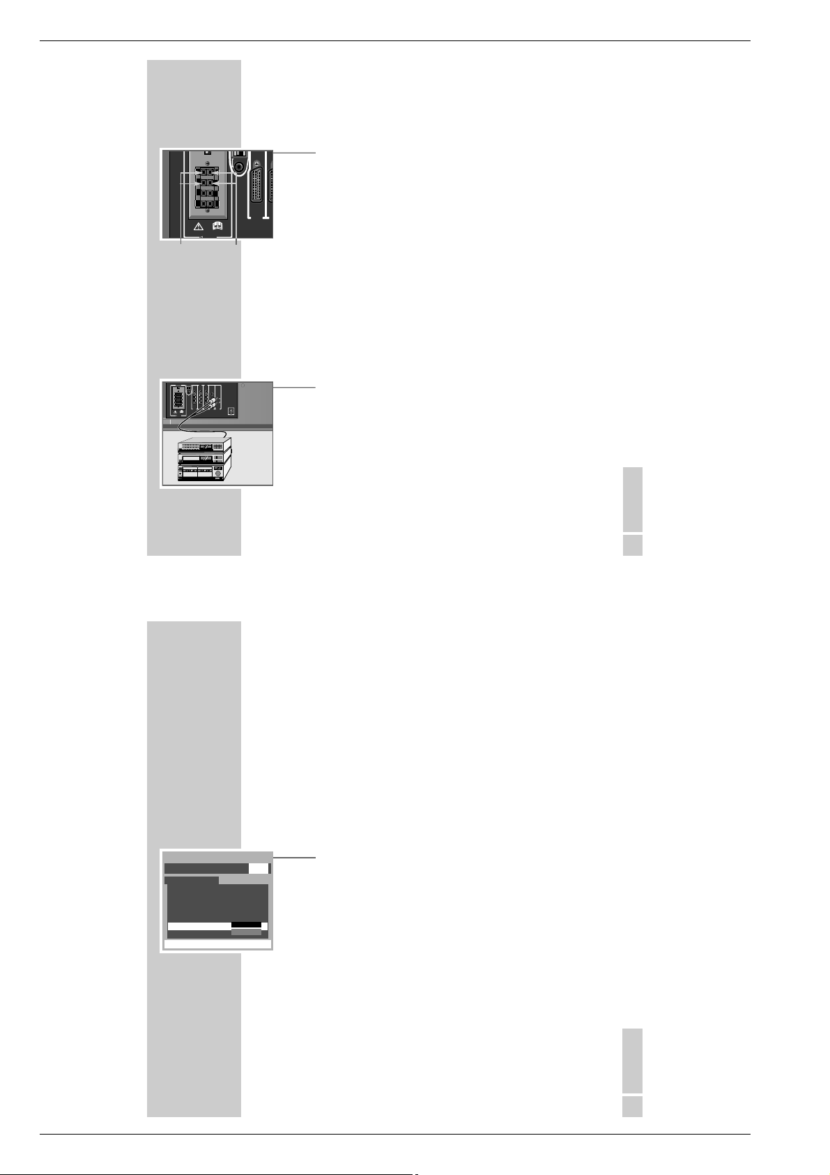
Kopfhöreranschluss
S-Video Bildsignaleingang für S-VHS Camerarecorder
Video Bildsignaleingang für VHS-Camerarecorder
L/Mono AUDIO R Tonsignaleingang für Camerarecorder)
6 IO Ein- und ausschalten
7 Menu Bild-/Tonmenü aufrufen
8
–
z + Lautstärke
9
–
P +
Wählt Programme auf/abwärts
10 EXIT Bild-/Tone
instellung beenden
ǵ
S-VIDEO
VIDEO L/MONO R
AUDIO
MENU
P
A
A
EXIT
ɦ
ɦ
ɦ
ɦ
A
Ƒ
(3)
8
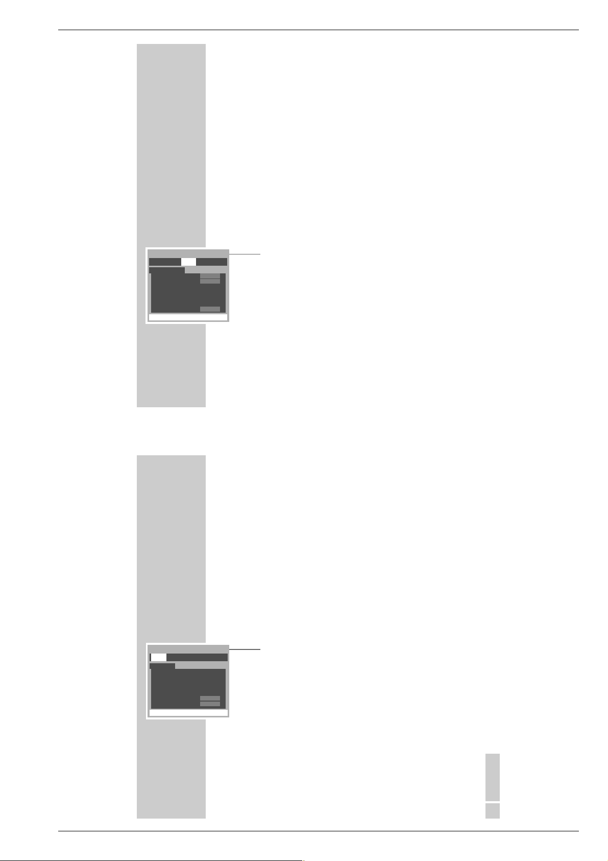
Die Rückseite des Fernsehgerätes
EXT INT Wahlschalter für Lautsprecher extern - Intern
MAIN Klemmbuchsen für Frontlautsprecher
SURROUND Klemmbuchsen für Surround-Lautsprecher
WOOFER EXT INT Anschluss und Wahlschalter für aktiven Subwoofer.
X(1) Euro/AV-Buchse (FBAS, RGB).
X(2) Euro/AV-Buchse (FBAS, S-VHS, Megalogic)
X(3) Euro/AV-Buchse (FBAS, S-VHS)
Y Pa/C
BPR/CR
Component Bildsignaleingang
OPTICAL/COAXIAL Digitaler Tonsignaleingang (PCM/Dolby Digital)
L AUDIO R Tonsignalausgang
Ä Antennenbuchse
AUF EINEN BLICK
__________________________________________________________________
Bedienhinweise Dieses Kapitel enthält Auszüge aus der Bedienungsanleitung. Weitergehende Informationen entnehmen Sie bitte der
gerätespezifischen Bedienungsanleitung, deren Materialnummer Sie in der Ersatzteilliste finden.
ccoro
ǵ
A
A
EXIT
MENU
A
P
(3)
A
Ƒ
ɦ
ɦ
ɦ
ɦ
VIDEO L/MONO R
S-VIDEO
AUDIO
!
I/II
ɾ
MAIN(8Ω)
WOOFER
ƴ
EXT INT
SURROUND
EXT. INT.
(+)
L
(-)
(-)
L
(+)
(8Ω)
(+)
R
(-)
(-)
R
(+)
OPTICAL COAXIAL
PCM/DOLBY DIGITAL
38
28
(S-VIDEO)
(S-VIDEO)
COMPONENT
VIDEO INPUT
Y
PB/C
B
L
PR/C
AUDIO
R
R
(1)
(3)
(4)
(2)
X
X
X
(AUDIO/VIDEO) (VIDEO) (FIXED)
Manufactured under license from Dolby Laboratories. “Dolby”, “Pro Logic” and the
double-D symbol are trademarks of Dolby Laboratories. Confidential Unpublished
Works. ©1992-1997 Dolby Laboratories, Inc. All right reserved.
(AUDIO/VIDEO)
1 - 4 GRUNDIG Service
ACCORO 102 Allgemeiner Teil / General Section
DEUTSCH
9
AUF EINEN BLICK
__________________________________________________________________
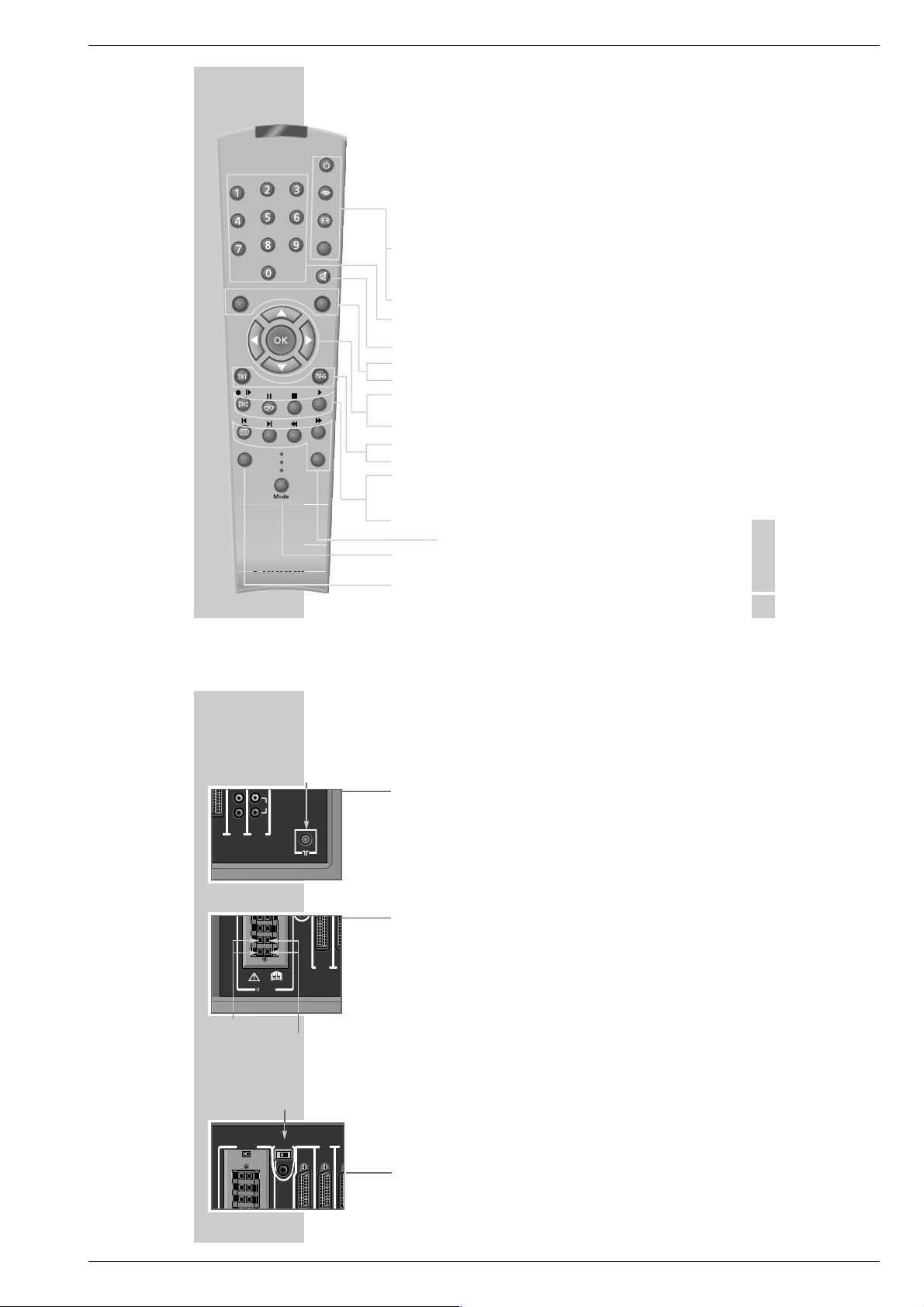
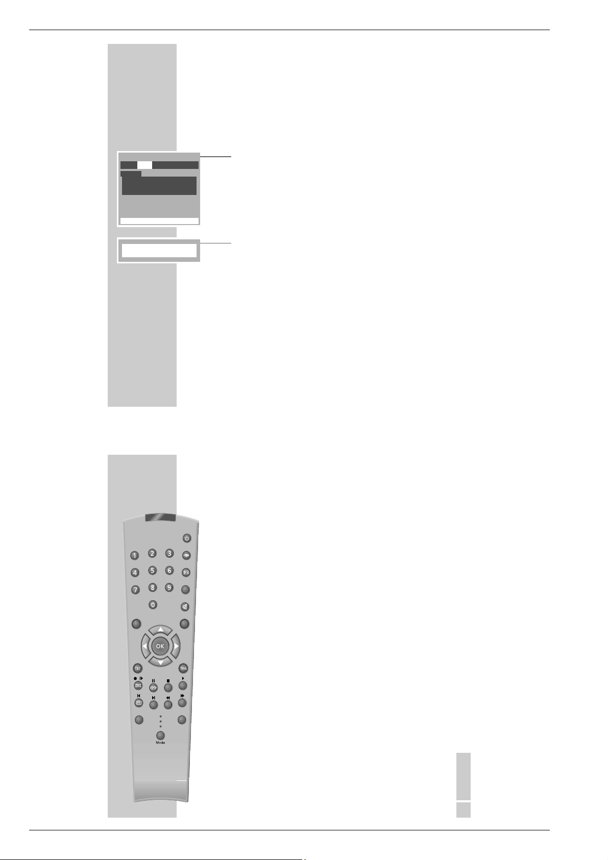
Die Fernbedienung
Mit der mitgelieferten Fernbedienung TP 130 können Sie nicht nur das
Fernsehgerät bedienen, sondern auch GRUNDIG Videorecorder, DVD-PLayer,
oder SAT-Receiver.
Bedienen des Fernsehgerätes
Schaltet das Fernsehgerät aus (Stand-by) und wieder ein
Bildvoreinstellungen 1, 2, 3 oder M (persönlich) aufrufen
Bildformat-Umschaltung.
AV AV-Stellung wählen
1 … 0 Programmwahl und Einschalten des Fernsehgerätes aus Stand-by.
Eingabe der Videotextseiten,
Ton ein/aus (stummschalten).
Menu DIALOG CENTER aufrufen
Exit Einstellungen beenden
Programmfortschaltung, Cursor nach oben/unten.
Lautstärke, Cursor nach links/rechts.
OK Ändern und aktivieren verschiedener Funktionen.
TXT Videotext-Betrieb, Media Window
TV-G TV-Guide
Blendet das Surround-Menü ein
Bassverstärkung
Mono/Stereo/Zweiton-Umschaltung
Call Programmanzeige ein/aus
Videotextfunktionen (siehe Kapitel Videotext)
Mode Umschaltung zwischen Grundig Satellitenreceiver (SAT), Videore-
corder (VCR) und DVD-Player (DVD)
Info Titel der aktuellen Sendung einblenden
ǵ
L
K
I/II
10
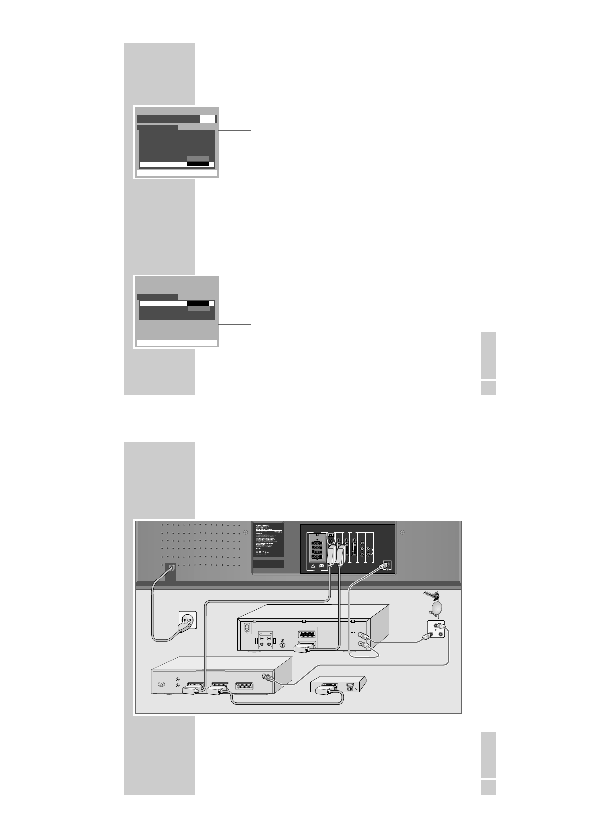
ANSCHLIESSEN UND VORBEREITEN
_____________
Antenne, Netzkabel anschließen
1 Antennenkabel der Hausantenne in die Antennenbuchse des Fernsehgerätes
stecken.
2 Stecker des Netzkabels in die Steckdose stecken.
Surround-Lautsprecher anschließen
1 Beiliegende Surround-Lautsprecher an die Klemmen »SURROUND«
anschließen.
Zum Einstecken des Lautsprecherkabels die Klemmhebel niederdrücken. Die
»–« Ader des Lautsprecherkabels in die schwarze (–) Klemme stecken. Die
»+« Ader (markierte oder farbige Ader) des Lautsprecherkabels in die rote
Klemme stecken.
Hinweis:
Werden Surround-Lautsprecher angeschlossen, muss dies im Menü »S«
unter Punkt »Surround-Einstellung« eingestellt werden (siehe Kapitel Dolby
Surround ProLogic).
Werden mehrere Boxen an die Klemmbuchse »SURROUND« angeschlossen, darf die gesamte Nennimpedanz von 8 Ohm nicht unterschritten
werden.
Externen aktiven Subwoofer anschließen
1 Subwoofer an die Buchse »WOOFER« anschließen.
2 Schalter »EXT INT« in Stellung »EXT« schieben.
– Der interne Subwoofer wird abgeschaltet.
f
PB/C
Antenne
e
a
b
I
X
(+)
(+)
SURROUND L
SURROUND R
WOOFER
B
PR/C
R
(3)
(4)
(VIDEO) (FIXED)
DIO/VIDEO)
olby Laboratories. “Dolby”, “Pro Logic” and the
Dolby Laboratories. Confidential Unpublished
ries, Inc. All right reserved.
R
(-)
(-)
R
(+)
L
AUDIO
R
L
(-)
(-)
L
(+)
(1)
X
(AUD
Manufactured under lic
double-D symbol are tr
SURROUND
(8Ω)
Works. ©1992-1997 Dol
GRUNDIG Service 1 - 5
(+)
R
(-)
(-)
R
MAIN(8Ω)
ƴ
EXT INT
WOOFER
EXT. INT.
(+)
L
(-)
(-)
L
28
(S-VIDEO)
(S-V
Allgemeiner Teil / General Section ACCORO 102
DEUTSCH
11
Externe Front-Lautsprecher anschließen
1 Externe Frontlautsprecher an die Klemmbuchsen »Main« anschließen
Dazu die Klemmhebel niederdrücken. Die »–« Ader des Lautsprecherkabels
stecken Sie in die schwarze (–) Klemme. Die »+« Ader (markierte oder farbige Ader) des Lautsprecherkabels stecken Sie in die rote Klemme.
2 Schalter »EXT INT« in Stellung »EXT«schieben.
– Die internen Lautsprecher wirken als Center-Lautsprecher.
Hinweis:
Die angeschlossenen Lautsprecher müssen mindestens eine Impedanz von 8
Ohm und eine Belastbarkeit von 14 W haben.
Der Schalter »EXT INT« darf nur bei angeschlossenen Front-Lautsprechern
auf »EXT« stehen.
HiFi-Anlage anschließen
Das Fernsehgerätes kann an Ihre HiFi-Anlage angeschlossen werden.
1 HiFi-Anlage an die Cinchbuchsen »L AUDIO R« anschließen.
ANSCHLIESSEN UND VORBEREITEN
_____________________________
e
EXT INT
X
FRONT L
FRONT R
Manufactured under license from Dolby Laboratories. “Dolby”, “Pro Logic” and the
double-D symbol are trademarks of Dolby Laboratories. Confidential Unpublished
Works. ©1992-1997 Dolby Laboratories, Inc. All right reserved.
AUDIO
L
R
(AUDIO/VIDEO) (VIDEO) (FIXED)
Y
(S-VIDEO)
(S-VIDEO)
COMPONENT
VIDEO INPUT
EXT.I NT.
EXT INT
(8Ω)
SURROUND
ƴ
MAIN(8Ω)
WOOFER
28
38
(1)
X
(2)
X
(AUDIO/VIDEO)
(3)
X
(4)
(+)
(-)
R
(+)
(-)
R
(+)
(-)
L
(+)
(-)
L
PB/C
B
PR/C
R
DEUTSCH
13
Ein-/ausschalten
1 Fernsehgerät mit »IO« am Fernsehgerät einschalten.
Leuchtet danach nur die LED »
«, befindet sich das Gerät in Bereitschaft.
Fernsehgerät mit »1…0«, »
« oder »« einschalten.
2 Fernsehgerät mit »
« in Bereitschaft (Stand-By) schalten.
– Fernsehgerät mit »1…0«, »
« oder » « einschalten.
3 Fernsehgerät mit »IO« am Fernsehgerät vollständig ausschalten.
– Sie sparen dadurch Energie.
Menüsprache einstellen
1 Info-Center mit »Menu« aufrufen.
2 Menü »S« mit »
« oder »« wählen
3 »Sprache« mit »
« wählen und mit »« oder »« gewünschte Sprache
auswählen.
4 Einstellung mit »Exit« beenden.
EINSTELLUNGEN
_____________________________________________________________
ANDERES MENÜ
EXIT : Menü verlassen
Ł
Ł
Ł
Ł
Ł
!
ĵŁ
!
ĵŁ
Ļ
s
AUS
DEUTSCH
(+)
R
(-)
(-)
R
(+)
EXT. INT.
(+)
L
(-)
(-)
L
(+)
(1)
X
Manufactured under lic
-
(AUDI
1 - 6 GRUNDIG Service

ACCORO 102 Allgemeiner Teil / General Section
14
Fernseh-Programme einstellen
Das Fernsehgerät ist mit einem automatischen Programmsuchlauf ausgestattet.
Sie starten den automatischen Suchlauf und können danach die Fernseh-Programme in der Reihenfolge Ihrer Wahl sortieren.
Wenn Sie einen GRUNDIG Video-Recorder mit MEGALOGIC-System über das
dem Videorecorder mitgelieferte Megalogic-EURO/AV (Scart)-Kabel an dieses
Fernsehgerät anschließen, dann ist das „Einstellen der Fernsehprogramme am
Video-Recorder“nicht mehr notwendig.
Wie das genau funktioniert, lesen Sie auf Seite 40, „Das GRUNDIG MegalogicSystem“.
Fernseh-Programme einstellen –
mit dem automatischen Suchlauf
1 Info-Center mit »Menu« aufrufen.
2 Menü »
« mit »« oder »« wählen
3 »System« mit »
« wählen und mit »« oder »« den Sendestandard
wählen. »B/G« für Kontinentales Europa; »D/K« für Osteuropa; »I« für
Großbritannien; »L1 (12)« oder »L2 (8)« für Frankreich
4 »Autom. Einstellung« mit »
« wählen und mit »« bestätigen.
– Die Seite »AUTOM. EINSTELLUNG« blendet sich ein.
5 – Suchlauf mit »OK« starten. Der Suchlauf kann – je nach Anzahl der zu
empfangenden Fernsehprogramme – eine Minute und länger dauern.
– Nach dem Suchlauf schaltet das Fernsehgerät auf Programmplatz 1 und
es wird die Programmtabelle eingeblendet.
EINSTELLUNGEN
____________________________________________________________________
EINSTELLUNG
EXIT : Menü verlassen
"
ĵŁ
#$
ĵŁ
$
Ł
Ł
%$$
Ł
Ł
%$$ &!
ĵŁ
s
AUS
B/G
AUTO
DEUTSCH
15
Gefundene Fernseh-Programme speichern
1 Das Fernsehprogramm das auf Programmplatz 1 gespeichert werden soll
mit »
« oder »« wählen und mit »OK« speichern.
2 Das Fernsehprogramm das auf Programmplatz 2 gespeichert werden soll
mit »« oder »« wählen und mit »OK« speichern.
3 Den oben beschriebenen Vorgang so oft wiederholen, bis alle Fernsehpro-
gramme gespeichert sind.
4 Einstellung mit »Exit« beenden.
Bild-Einstellungen
1 Dialog Center mit »Menu« aufrufen.
2 Menü »
« mit »« oder »« wählen.
3 Zeile »Kontrast«, »Helligkeit«, »Farbe«, »Farbton« oder
»Schärfe« mit »« oder »« wählen.
4 Einstellung mit »
« oder »« verändern und mit »OK« bestätigen..
5 »SCAN MODE« (Zeilenreduktion) mit »
« oder »« wählen und mit
»« oder »« die Einstellung »100 Hz« oder »Natürlich« (=Ein) wählen.
6 »DNR« (Rauschunterdrückung) mit »
« oder »« wählen und mit »«
oder »« die Einstellung »Aus« oder »Auto« wählen.
7 Beenden mit »Exit«.
EINSTELLUNGEN
____________________________________________________________________
BILD
EXIT : Menü verlassen
' 68
ĵŁ
(& 93
ĵŁ
" 71
ĵŁ
" 00
ĵŁ
) + 21
ĵŁ
$
ĵŁ
*+
ĵŁ
s
–––––●–––
–––––––
●
–
––––––
●
––
––––
●
––––
––––
●
––●–
AUTO
100Hz
GRUNDIG Service 1 - 7

Allgemeiner Teil / General Section ACCORO 102
16
Toneinstellungen
Bässe, Höhen und Balance verändern
1 Dialog Center mit »Menu« aufrufen.
2 Menü »
« mit »« oder »« wählen.
3 »Bass«, »Höhen«, »Balance« mit »
« oder »« wählen.
4 Einstellung mit »
« oder »« verändern und mit »OK« bestätigen..
5 Beenden mit »Exit«.
Interne Bassverstärkung verändern
1 Bassverstärkung mit » « ein-/ausschalten. Die Einblendung »Bassverst.
Int.« erscheint.
2 Bei Bassverstärkung ein Wert mit »
« oder »« verändern. Die Einblen-
dung erlischt nach kurzer Zeit.
EINSTELLUNGEN
____________________________________________________________________
TON
EXIT : Menü verlassen
+ 46
ĵŁ
(, + 43
ĵŁ
00
ĵŁ
s
––––●–––
●
––––●–––
●
––––●––––
Bassverstär. int. 46
––––––––––––––––●–––––––––––––––
DEUTSCH
21
Grundfunktionen
Programmplätze anwählen
1 Programmplätze mit »1...0« direkt wählen.
Nach Eingabe der ersten Ziffer erscheint ein Strich neben der ersten Zahl.
Solange dieser Strich dargestellt wird, kann die zweite Ziffer für einen zweistelligen Programmplatz eingegeben werden.
2 Programmplätze mit »
« oder »« schrittweise wählen.
3 Programmplatz AV1 – AV4 mit »AV« wählen
(Anzeige am Bildschirm »EXT1« – »EXT4«).
Lautstärke ändern
1 Lautstärke mit »
« oder »« ändern.
Ton ein-/ausschalten
1 Ton mit » « ein- oder ausschalten (stummschalten).
Untertitel
1 Untertitel ein-/ausblenden, dazu »F« gedrückt halten und »Info« drücken
(nur möglich, wenn Untertitel zur laufenden Sendung angeboten werden).
Uhrzeit ein-/ausblenden
1 Uhrzeit ein-/ausblenden, dazu »F« gedrückt halten und »
« drücken.
(Nur bei Fernseh- Programmen mit Videotext).
FERNSEH-BETRIEB
__________________________________________________________
ǵ
L
K
I/II
1 - 8 GRUNDIG Service
ACCORO 102 Allgemeiner Teil / General Section
22
Mono, Stereo Zweiton Umschaltung
Empfängt das Gerät Zweiton-Sendungen (Anzeige an der Vorderseite »I/II«) –
z.B. einen Spielfilm im Originalton auf Tonkanal 2 und die synchronisierte Fassung auf Tonkanal 1 – so können Sie den von Ihnen gewünschten Tonkanal
wählen.
Empfängt das Gerät Stereo-Sendungen, schaltet es automatisch auf Stereo-Tonwiedergabe (Anzeige an der Vorderseite »
«).
Bei schlechter Stereo-Ton-Empfangsqualität können Sie den Ton auf »Mono«
schalten.
1 Gewünschten Einstellung mit »
« wählen. Die gewählte Einstellung wird
am Bildschirm angezeigt.
Programminformation
Wenn NextView eingeschaltet ist, kann der Titel der aktuellen Sendung am Bildschirm eingeblendet werden.
1 Mit »Info« Programminformation ein-/ausblenden.
Bildeinstellungen
1 Mit »z«die Vorprogrammierten Einstellungen »Bild -1«, »Bild -2«,
»Bild -3« oder die persönliche Bildeinstellung » Bild - M« wählen.
FERNSEH-BETRIEB
__________________________________________________________________
ǵ
L
K
I/II
DEUTSCH
23
FERNSEH-BETRIEB
__________________________________________________________________
Bildformat-Umschaltung
1 Bildformat mit »
E
« anwählen, am Bildschirm erscheint das gewählte Bildformat, zum Beispiel »Breitwand-Zoom«.
– Sie können zwischen folgenden Bildformaten wählen:
Herkömmlich 4:3
Bei dieser Einstellung sind bei herkömmlichen 4:3 Sendungen links und rechts
schwarze Streifen.
Super Live
Diese Betriebsart eignet sich für Kinofilme mit extremen Breiten-Höhenverhältnissen.
Bei 4:3 Sendungen – und gewählter Funktion »Super Live« – erscheint das Bild
horizontal verbreitert. Die Bildgeometrie wird in horizontaler Richtung gedehnt.
Kino-Zoom, Kino-Zoom mit Untertitel
Dieses Format eignet sich besonders für Sendungen im Format 16:9.
Die bisher üblichen schwarzen Streifen oben und unten im Bild werden über-
schrieben.
4:3 Bilder werden formatfüllend gezeigt.
Die gesendeten Bilder werden vergrößert, dabei geht oben und unten etwas
Bildinhalt verloren. Die Bildgeometrie bleibt aber erhalten.
Beim Format Kino-Zoom mit Untertiteln, wird das Bild etwas nach oben geschoben, so dass Untertitel zum Film lesbar sind.
GRUNDIG Service 1 - 9
Allgemeiner Teil / General Section ACCORO 102
24
FERNSEH-BETRIEB
__________________________________________________________________
14:9
Bei dieser Einstellung wird das Bild etwas vergrößert. Wie beim Bildformat
»Herkömml. 4:3« sind links und rechts schwarze Streifen.
Breitwand-Zoom
Bei 16:9 Sendungen oder Signalquellen – z.B von einem Beistell-Decoder oder
Settop-Decoder über die Euro-AV-Buchse zugeführt – ist das Bild voll ausgefüllt
und die Bildgeometrie korrekt.
Bei 4:3 Sendungen erscheint das Bild horizontal verbreitert.
Die Bildgeometrie wird in horizontaler Richtung linear gedehnt.
Horizontale und vertikale Bildanpassung
Die Bildlage kann horizontal (nach links/rechts) angepasst werden. Beim Format »Kino Zoom« und »Kino-Zoom mit Untertitel« kann die Bildlage zusätzlich
auch noch vertikal (nach oben/unten) angepasst werden.
1 Dialog Center mit »Menu« aufrufen und Menü »S« mit »
« oder »«
wählen.
2 »Bildlage « mit »
« wählen und mit »« aufrufen.
3 »Bildlage Horizontal « oder »Bildlage Vertikal« mit »
« wählen und Bildla-
ge mit »« oder »« verändern.
4 Beenden mit »Exit«.
BILDLAGE
EXIT : Menü verlassen
-.&
(/
Ł
&
Ł
36
KOMFORTFUNKTIONEN
_________________________________________
Kindersicherung
Für die Kindersicherung haben Sie zwei Möglichkeiten. Bei beiden Möglichkeiten müssen Sie dafür sorgen, die Fernbedienung außerhalb der Reichweite
Ihrer Kinder aufzubewahren.
Pr
ogramm skip:
Sie können einzelne Programmplätze sperren. Die nichtgesperrten Programmplätze können mit den Tasten an der Vorderseite des Fernsehgerätes gewählt
werden. Gesperrte Programmplätze werden übersprungen und können nur
noch mit »1...0« der Fernbedienung gewählt werden. Wird ein gesperrter Programmplatz mit der Fernbedienung gewählt, erscheint als Hinweis vor der Programmanzeige ein ✴, z.B » ✴ 3«.
Bedienfelds
perre:
Damit werden die Tasten an der Vorderseite des Fernsehgerätes gesperrt. Das
Fernsehgerät ist ohne Fernbedienung nicht mehr zu bedienen.
Programm skip
1 Das Fernsehprogramm wählen, das gesperrt werden soll.
2 Dialog Center mit »Menu« aufrufen und Menü » « mit »
« oder
»
« wählen.
3 »Programm skip « mit »
« wählen.
4 Mit »
« »EIN« wählen.
Der Programmplatz ist gesperrt.
5 Beenden mit »Exit«.
6 Schritte 1 – 4 so oft wiederholen, bis alle gewünschten Programmplätze
gesperrt sind.
EINSTELLUNG
EXIT : Menü verlassen
"
ĵŁ
#$
ĵŁ
$
Ł
Ł
%$$
Ł
g
Ł
%$$ &!
ĵŁ
s
AUS
B/G
AUTO
1 - 10 GRUNDIG Service
ACCORO 102 Allgemeiner Teil / General Section
DEUTSCH
37
Bedienfeldsperre
1 Dialog Center mit »Menu« aufrufen und Menü »S« mit »
« oder »«
wählen.
2 »Bedienfeldsperre « mit »
« wählen.
3 Mit »
« »EIN« wählen.
4 Beenden mit »Exit«.
5 Fernsehgerät mit der Netztaste ausschalten.
Das Bedienfeld ist gesperrt. Das Fernsehgerät läßt sich nach dem Einschalten mit der Netztaste nur noch mit der Fernbedienung einschalten.
Hinweis:
Wird bei gesperrtem Bedienfeld eine Taste an der Vorderseite des Fernsehgerätes gedrückt, erscheint die Einblendung »Bedienfeldsperre «.
Formaterkennung
Ist diese Funktion aktiviert, schaltet das Fernsehgerät bei Breitbildübertragun-
gen, z.B. von einem DVD-Player automatisch auf das Breitbildformat.
1 Dialog Center mit »Menu« aufrufen und Menü »S« mit »
« oder »«
wählen.
2 »WSS « (2. Seite der Menütafel) mit »
« wählen und mit auf »« »EIN«
schalten.
3 Beenden mit »Exit«.
KOMFORTFUNKTIONEN
____________________________________________________
ANDERES MENÜ
EXIT : Menü verlassen
Ł
Ł
Ł
Ł
Ł
!
ĵŁ
!
ĵŁ
Ļ
s
AUS
DEUTSCH
ANDERES MENÜ
EXIT : Menü verlassen
0
ĵŁ
1
ĵŁ
'2/
Ł
AUS
EIN
DEUTSCH
39
DEUTSCH
Anschlussbeispiel mit Videorecorder,
Satellitenreceiver und Decoder
Hinweise:
Wenn Ihr Videorecorder mit Megalogic Plus ausgestattet ist, muss der
Videorecorder mit dem dem Videorecorder beiliegenden EURO-AV-Kabel
an der Euro-AV-Buchse »X(2)« angeschlossen werden.
BETRIEB MIT EXTERNEN GERÄTEN
_________________
Manufactured under license from Dolby Laboratories. “Dolby”, “Pro Logic” and the
double-D symbol are trademarks of Dolby Laboratories. Confidential Unpublished
Works. ©1992-1997 Dolby Laboratories, Inc. All right reserved.
AUDIO
L
R
(AUDIO/VIDEO) (VIDEO) (FIXED)
Y
(S-VIDEO)
(S-VIDEO)
COMPONENT
VIDEO INPUT
EXT. INT.
EXT INT
(8Ω)
SURROUND
ƴ
MAIN(8Ω)
WOOFER
28
38
(1)
X
(2)
X
(AUDIO/VIDEO)
(3)
X
(4)
(+)
(-)
R
(+)
(-)
R
(+)
(-)
L
(+)
(-)
L
PB/C
B
PR/C
R
TV R
SAT
220-240 V
~
50-60 Hz
EURO AV VCREURO AV DECODEREURO AV TV
AUDIO OUT
R
L
INPUT-SAT
950-2150 MHz
14/18 V 450 mA
R
L
AUDIO
R
L
I
N
O
U
T
2 EXTERNAL / DEC. - AV 2
1 EXTERNAL / EURO - AV 1
PAY-TV
Videorecorder
Satellitenreceiver
Decoder
GRUNDIG Service 1 - 11
Allgemeiner Teil / General Section ACCORO 102
DEUTSCH
45
DEUTSCH
SONDERFUNKTIONEN
______________________________________________
Fernseh-Programme einstellen –
durch manuelle Eingabe
Diese Einstellung ist nur dann erforderlich, wenn ein neues Fernseh-Programm
hinzukommt
1 Info-Center mit »Menu« aufrufen.
2 Das Menü »
« mit »« oder »« wählen
3 »Manuelle Einstellung« mit »
« wählen und mit »« bestätigen.
– Die Seite »MANUELLE. EINSTELLUNG« erscheint.
4 Suchlauf mit » OK« starten. Am Bildschirm erscheint »>>>«.
Der Suchlauf stoppt, wenn ein Programm gefunden wurde.
Ist es nicht das richtige Fernsehprogramm, Suchlauf erneut mit »OK« starten.
5 »Programm-Nummer« mit »
« wählen und gewünschten Programmplatz
mit »
« oder »« schrittweise oder mit »1...0« direkt eingeben.
6 Der Programmname wird in den meisten Fällen vom Fernsehgerät automa-
tisch erkannt. Ist das nicht der Fall, die Zeile »SENDERNAME« mit »
«
wählen und mit »« oder »« den gewünschten Namen auswählen.
7 Speichern mit »OK«.
8 Beenden mit »Exit«.
Hinweis:
Ist die neue Kanalnummer bekannt, kann diese direkt eingegeben werden.
In diesem Fall ist unter Pkt 4 die Zeile »Kanal« zu wählen. Die Kanalzahl
kann mit »
« oder »« schrittweise oder mit »1...0« direkt eingegeben
werden.
MANUELLE EINSTELLUNG
: Speichern
: Menü verlassen
-.&
ĵŁ
%$$$$
ĵŁ
'
Ł
$
ĵŁ
+
3
456
78
46
SONDERFUNKTIONEN
________________________________________________________
Feinabstimmung
Das Gerät stimmt automatisch auf beste Bild- und Tonqualität ab.
Bei schwierigen Empfangsverhältnissen kann es in Einzelfällen notwendig sein,
die Bild- und Tonqualität durch Feinabstimmen zu optimieren.
1 Info-Center mit »Menu« aufrufen.
2 Das Menü »
« mit »« oder »« wählen
3 »Feineinstellung« mit »
« wählen und mit »« bestätigen.
4 Mit »
« oder »« auf beste Bild und Tonqualität abstimmen.
5 Beenden mit »Exit«.
Fernsehprogramme wechseln
Beispiel: Das Programm von Programmplatz 5 soll auf Programmplatz 2.
1 Info-Center mit »Menu« aufrufen.
2 Das Menü »
« mit »« oder »« wählen
3 »Programm wechseln« mit »
« wählen und mit »« bestätigen.
– Die Seite »PROGRAMM WECHSELN« erscheint.
4 Programmplatz 5 mit »
« wählen und mit »OK« bestätigen.
5 Programmplatz 2 mit »
« oder »« wählen und mit »OK« bestätigen.
Das Fernsehprogramm vom Programmplatz 5 befindet sich jetzt auf Programmplatz 2.
6 Beenden mit »Exit«.
Feineinstellung
––––––––––––––––●–––––––––––––––
PROGRAMM WECHSELN
ENTER : Auswählen EXIT : Verlassen
Prog. SendernameļKanal
1 ARD 6
2 ZDF 34
3 BR-3 59
4 RTL 36
Ļ
1 - 12 GRUNDIG Service

ACCORO 102 Allgemeiner Teil / General Section
DEUTSCH
47
SONDERFUNKTIONEN
________________________________________________________
Blauer Bildschirm wählen
Mit dieser Einstellung wird bei verrauschtem Bild auf ein blaues Bild umgeschaltet. Der Ton wird abgeschaltet. Nach ca. 20 Minuten schaltet das Fernsehgerät auf Bereitschaft (Stand-by).
1 Dialog Center mit »Menu« aufrufen und Menü »S« mit »
« oder »«
wählen.
2 »B/B « mit »
« wählen (zweite Seite der Menütafel).
3 Mit »
« oder »« »EIN « wählen.
4 Beenden mit »Exit«.
ANDERES MENÜ
EXIT : Menü verlassen
WSS
ĵŁ
B/B
ĵŁ
Konvergenz
Ł
AUS
EIN
48
SONDERFUNKTIONEN
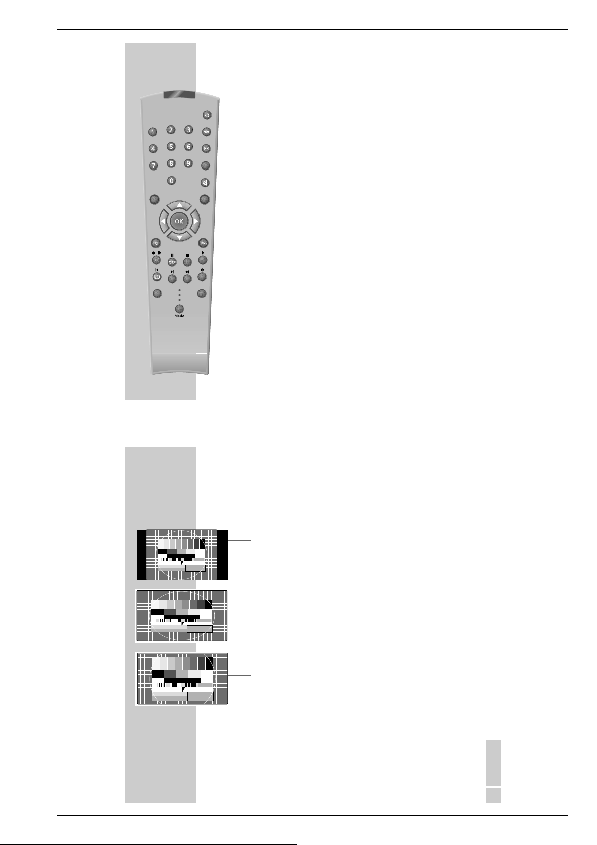
________________________________________________________
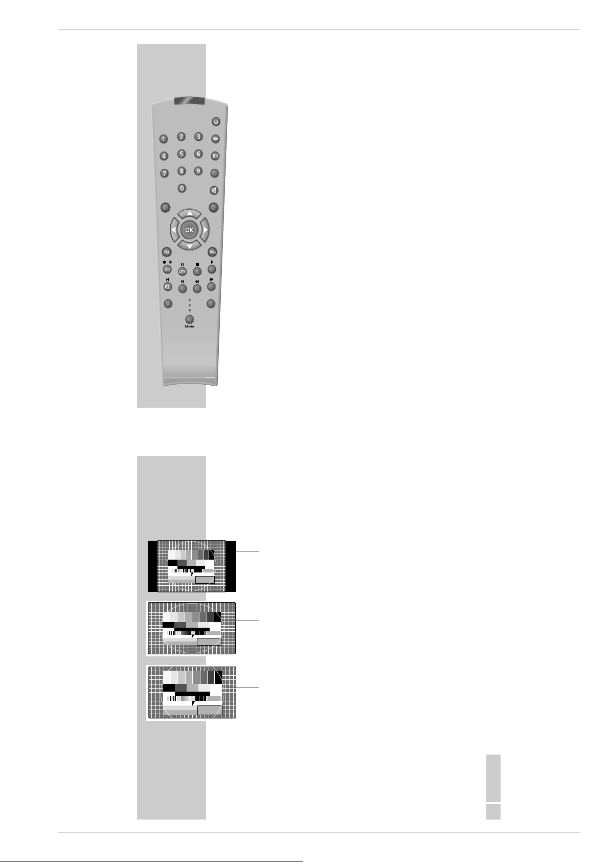
Konvergenz einstellen
Bei Ihrem Fernsehgerät werden die drei Grundfarben Rot, Grün und Blau
getrennt auf den Bildschirm projeziert. Die drei Farben müssen genau zueinander abgestimmt sein. In der Regel muss diese Einstellung nicht verändert werden. Sollte das Bild aber unscharfe Ränder oder verschwommene Farben aufweisen, kann die Konvergenz eingestellt werden.
1 Dialog Center mit »Menu« aufrufen und Menü »S« mit »
« oder »«
wählen.
2 »Konvergenz « mit »
« wählen (zweite Seite der Menütafel) und mit »«
aufrufen. Am Bildschirm erscheint ein Kreuz und neun nummerierte Rechtecke.
3 »Rote Taste« drücken.
4 Mit »
«, »«, »« und »« die rote Farbe deckungsgleich auf das
weiße Kreuz schieben, so dass kein Schatten mehr sichtbar ist.
5 »Blaue Taste« drücken und den Vorgang für die blaue Farbe wieder-
holen.
6 Konvergenz der Bildränder einstellen, dazu jeweils das entsprechende
Rechteck mit den Zifferntasten »1...9« aufrufen und die obenbeschriebene
Einstellung der Farbe rot und blau für jedes Rechteck durchführen.
7 Beenden mit »Exit«.
ANDERES MENÜ
EXIT : Menü verlassen
0
ĵŁ
1
ĵŁ
'2/
Ł
AUS
EIN
GRUNDIG Service 1 - 13

Allgemeiner Teil / General Section ACCORO 102
ENGLISH
7
AT A GLANCE
___________________________________________________________________
The front of the TV set
ї
Headphones connector
S-Video Video input for S-VHS camcorder
Video Video input for für VHS camcorder
L/Mono AUDIO R Audio input for camcorder
6 IO On/off switch
7 Menü Select Picture/Sound menu button
8
–
z + Volume control
9
–
P +
Select channel up/down button
10 EXIT End picture/sound settings
button
ǵ
S-VIDEO
VIDEO L/MONO R
AUDIO
MENU
P
A
A
EXIT
ɦ
ɦ
ɦ
ɦ
A
Ƒ
(3)
8
The rear of the TV set
EXT INT External/internal loudspeaker selector switch
MAIN Terminals for front loudspeakers
SURROUND Terminals for surround loudspeakers
WOOFER EXT INT Terminal and selector switch for active subwoofer
X(1) Euro/AV socket (CCS, RGB).
X(2) Euro/AV socket (CCS, S-VHS, Megalogic)
X(3) Euro/AV socket (CCS, S-VHS)
Y Pa/C
BPR/CR
Component picture signal input
OPTICAL/COAXIAL Digital audio signal input (PCM/Dolby Digital)
L AUDIO R Audio signal output
Ä Aerial input
AT A GLANCE
__________________________________________________________________________
Operating Hints This chapter contains excerpts from the user manual. For further particulars please refer to the appropriate user manual
the part number of which is indicated in the spare parts list.
ccoro
ǵ
A
A
EXIT
P
A
MENU
(3)
A
Ƒ
ɦ
ɦ
ɦ
VIDEO L/MONO R
S-VIDEO
AUDIO
!
I/II
ɦ
ɾ
OPTICAL COAXIAL
PCM/DOLBY DIGITAL
MAIN(8Ω)
WOOFER
ƴ
EXT INT
(+)
R
(-)
(-)
R
(+)
EXT. INT.
(+)
L
(-)
(-)
L
(+)
Manufactured under license from Dolby Laboratories. “Dolby”, “Pro Logic” and the
double-D symbol are trademarks of Dolby Laboratories. Confidential Unpublished
SURROUND
(8Ω)
Works. ©1992-1997 Dolby Laboratories, Inc. All right reserved.
28
(S-VIDEO)
(S-VIDEO)
(1)
(2)
X
X
X
(AUDIO/VIDEO) (VIDEO) (FIXED)
(AUDIO/VIDEO)
38
COMPONENT
VIDEO INPUT
Y
PB/C
B
L
PR/C
AUDIO
R
R
(3)
(4)
1 - 14 GRUNDIG Service
ACCORO 102 Allgemeiner Teil / General Section
ENGLISH
9
AT A GLANCE
__________________________________________________________________________
The remote control
With the remote TP 130 supplied you can operate not only the TV set, but also
GRUNDIG video recorders, DVD pLayers, or SAT receivers.
Remote control of the TV set
Switches the TV set off (standby) and on again.
Selects picture presettings 1, 2, 3 or M (personal).
Switches the picture format.
AV Selects the AV position.
1 … 0 Direct channel selection and switching the TV set on from standby.
Entry of teletext pages.
Sound on/off (mute function)
Menu Calls up the DIALOG CENTER
Exit Ends the settings
Channel positions up/down, cursor up/down.
Volume, cursor to the left/right.
OK Changes and activates various functions.
TXT Teletext mode, Media Window
TV-G TV-Guide
Displays the Surround menu.
Bass boost
Mono/stereo/two-channel sound switch-over
Call Switches the programme indication on/off
Teletext functions (see Teletext chapter)
Mode Switch-over between Grundig satellite receiver (SAT), video
recorder (VCR), and DVD player (DVD).
Info Displays the title of the current programme
ǵ
L
K
I/II
10
CONNECTION AND PREPARATION
_______________
Connecting the aerial and the mains cables
1
Connect the cable from the house aerial with the aerial input of your TV set.
2
Connect the mains cable with a wall outlet.
Connecting the surround loudspeakers
1
Connect the surround loudspeakers supplied with the »SURROUND«
terminals.
To insert the loudspeaker cables, press down the clamping levers. Insert the
»–« core of the loudspeaker cable into the black (–) terminal and the »+« core
(marked or coloured core) into the red terminal.
Note:
If surround loudspeakers are connected, this configuration must be selected
in the »S« menu under the point »Surround settings« (see chapter Dolby
Surround ProLogic).
If several loudspeakers are connected to the »SURROUND« terminal, the
total nominal impedance is not allowed to fall below 8 Ohm.
Connecting an active subwoofer
1
Connect the subwoofer to the »WOOFER« terminal.
2
Slide the »EXT INT« switch to the »EXT« position.
– The internal subwoofer is switched off.
f
P
Aerial
e
a
b
I
X
(+)
(+)
SURROUND L
SURROUND R
WOOFER
GRUNDIG Service 1 - 15
B/CB
L
PR/C
AUDIO
R
R
(3)
(4)
(VIDEO) (FIXED)
DIO/VIDEO)
olby Laboratories. “Dolby”, “Pro Logic” and the
Dolby Laboratories. Confidential Unpublished
ries, Inc. All right reserved.
R
(-)
(-)
R
(+)
ƴ
EXT INT
(+)
R
(-)
(-)
R
L
(-)
(-)
L
(+)
SURROUND
(8Ω)
(1)
X
Manufactured under lic
double-D symbol are tr
Works. ©1992-1997 Dol
(AUD
MAIN(8Ω)
WOOFER
EXT. INT.
(+)
L
(-)
(-)
L
(S-VIDEO)
28
(S-V
Allgemeiner Teil / General Section ACCORO 102
ENGLISH
11
Connecting external front loudspeakers
1
Connect the external front loudspeakers to the »Main« terminals.
To insert the loudspeaker cable, press down the clamping levers. Insert the
»–« core of the loudspeaker cable into the black (–) terminal and the »+« core
(marked or coloured core) into the red terminal
2
Slide the »EXT INT« switch to the »EXT« position.
– The internal loudspeakers now operate as centre loudspeakers.
Note:
The connected loudspeakers must have an impedance of at least 8 Ohm and
a power-handling capacity of 14W.
The »EXT INT« switch is allowed to be set to the »EXT« position only if
front loudspeakers are connected.
Connecting a hifi system
You may connect your TV set to your hifi system.
1
Connect the hifi system to the »L AUDIO R« phono sockets.
CONNECTION AND PREPARATION
_______________________________
e
EXT INT
X
FRONT L
FRONT R
Manufactured under license from Dolby Laboratories. “Dolby”, “Pro Logic” and the
double-D symbol are trademarks of Dolby Laboratories. Confidential Unpublished
Works. ©1992-1997 Dolby Laboratories, Inc. All right reserved.
AUDIO
L
R
(AUDIO/VIDEO) (VIDEO) (FIXED)
Y
(S-VIDEO)
(S-VIDEO)
COMPONENT
VIDEO INPUT
EXT.INT.
EXT INT
(8Ω)
SURROUND
ƴ
MAIN(8Ω)
WOOFER
28
38
(1)
X
(2)
X
(AUDIO/VIDEO)
(3)
X
(4)
(+)
(-)
R
(+)
(-)
R
(+)
(-)
L
(+)
(-)
L
PB/C
B
PR/C
R
ENGLISH
13
Switching the TV set on/off
1
Press the »IO« button on the TV set to switch the TV set on.
If, after doing this, only the »
« LED is lit, then the TV set is in standby.
Press one of the buttons »1…0«, »
« or »« to switch the TV set on.
2
Press the »« button to switch the TV set to standby.
– Press one of the buttons »1…0«, »
« or »« to switch the TV set on.
3
Press the »IO« button on the TV set to switch definitely off.
– This will save energy.
Selecting the dialogue language
1
Call up the Dialog Center using the »Menu« button.
2
Select the »S« menu using the »« or »« button.
3
Select the »Language « row using the »« button then select the desired
language using the »
« or »« button.
4
Press »Exit« to end the setting.
SETTINGS
______________________________________________________________________________
FEATURE MENU
EXIT :To exit
Ł
% !
Ł
Ł
!
Ł
!
Ł
9
ĵŁ
% &
ĵŁ
Ļ
s
OFF
ENGLISH
(+)
R
(-)
(-)
R
(+)
EXT. INT.
(+)
L
(-)
(-)
L
(+)
(1)
X
Manufactured under lic
-
(AUDI
1 - 16 GRUNDIG Service
ACCORO 102 Allgemeiner Teil / General Section
14
Programming TV channels
The TV set is equipped with an automatic tuning system.
When the automatic tuning function is completed, you can sort the found TV
channels to suit your taste.
If you connect a GRUNDIG video recorder which is equipped with the MEGALOGIC system to this TV set using the Megalogic EURO/AV (Scart) cable
supplied with the video recorder, programming of TV channels on the video
recorder is no more required.
For more information, see page 40, chapter “The GRUNDIG Megalogic
System”.
Programming TV channels using the automatic
tuning system
1
Call up the Dialog Center using the »Menu« button.
2
Select the »« menu using the »« or »« button.
3
Select »System« using the »« button, then use the »« or »« button to
select the transmission standard: »B/G« for Continental Europe, »D/K« for
East Europe, »I« for Great Britain, »L1 (12)« or »L2 (8)« for France.
4
Select »Auto tune« using the »« button then confirm with »«.
– The »AUTO TUNE« screen appears.
5
– Press »OK« to start the automatic tuning system. Depending on the
number of receivable channels, the channel search may take one minute
or longer.
– When the automatic channel search is completed, the TV set switches to
channel position 1 and the programme list appears on the picture screen.
SETTINGS
__________________________________________________________________________________
SET UP
EXIT :To exit
ĵŁ
#$
ĵŁ
Ł
Ł
%$$ !
Ł
Ł
%$$ &!
ĵŁ
s
OFF
B/G
AUTO
ENGLISH
15
Storing the found TV channels
1
Select the TV channel which is to be stored on channel position 1 using the
»
« or »« button then press »OK« to store the channel.
2
Select the TV channel which is to be stored on channel position 2 using the
»
« or »« button then press »OK« to store the channel.
3
Repeat the same procedure until all found TV channels are stored.
4
Press the »Exit« button to end the setting.
Picture settings
1
Call up the Dialog Center using the »Menu« button.
2
Select the »« menu using the »« or »« button.
3
Select the »Contrast«, »Brightness«, »Colour«, »Tint« or »Sharpness« row
using the »
« or »« button.
4
Change the setting using the »« or »« button then confirm with »OK«.
5
Select »Scan mode« using the »« or »« button then use the »« or
»
« button to select »100 Hz« or »Natural« (= On) .
6
Select »DNR« (noise reduction) using the »« or »« button then use the
»
« or »« button to select »OFF« or »AUTO«.
7
Press the »Exit« button to end the setting.
SETTINGS
__________________________________________________________________________________
PICTURE
EXIT :To exit
68
ĵŁ
93
ĵŁ
71
ĵŁ
00
ĵŁ
! + 21
ĵŁ
$
ĵŁ
*+
ĵŁ
s
–––––●–––
–––––––
●
–
––––––
●
––
––––
●
––––
––––
●
––●–
AUTO
100Hz
GRUNDIG Service 1 - 17
Allgemeiner Teil / General Section ACCORO 102
16
Sound settings
Changing the bass, treble and balance settings
1
Call up the Dialog Center using the »Menu« button.
2
Select the »« menu using the »« or »« button.
3
Select »Bass«, »Treble, or »Balance« using the »« or »« button.
4
Change the setting using the »« or »« button then confirm with »OK«.
5
Press the »Exit« button to end the setting.
Changing the internal bass boost
1
Use the »« button the switch the bass boost on and off. The »Bass
boost« display apperars.
2
Use the »« or »« button to change the bass boost setting. The display
disppears after a few moments.
SETTINGS
__________________________________________________________________________________
SOUND
EXIT :To exit
+ 46
ĵŁ
" + 43
ĵŁ
00
ĵŁ
s
––––●–––
●
––––●–––
●
––––●––––
Bass boost 46
––––––––––––––––●–––––––––––––––
ENGLISH
21
Basic functions
Selecting channel positions
1
Select the channel positions directly using the »1...0« buttons.
After entering the first digit a dash appears next to the first digit. As long as
this dash is visible, you may enter the second digit for two-digit channel
positions.
2
Use the »« or »« button to select the channel positions step by step.
3
Select the channel positions AV1 – AV4 using the »AV« button
(indication on the picture screen »EXT1« – »EXT4«).
Adjusting the volume
1
Adjust the volume with »« or »«.
Switching the sound on/off
1
Use the »« button to switch the sound on and off (mute).
Subtitles
1
Display or suppress subtitles be pressing and holding down the»F« button
while pressing the »INFO« button (only possible if subtitles are offered for
the current programme).
Switching the clock time indication on/off
1
Display or suppress subtitles be pressing and holding down the»F« button
while pressing the »
« button.
(Only possible on programmes with teletext).
TV MODE
______________________________________________________________________________
ǵ
L
K
I/II
1 - 18 GRUNDIG Service
ACCORO 102 Allgemeiner Teil / General Section
22
Mono, stereo, two-channel sound
If the TV set receives two-channel sound transmissions (»I/II« indication at the
front) – e.g. a film in the original version on sound channel 2 and the synchronized version on sound channel 1 – then you may select the desired sound
channel.
If the TV set receives stereo transmissions, it switches automatically to stereo
sound (»
« indication at the front).
If stereo reception is poor, the sound should be switched to »Mono«.
1
Select the desired sound mode using the »« button. The selected setting
is indicated on the picture screen.
Programme information
If the NextView function is activated, you may display the title of the current
programme on the picture screen.
1 Use the »Info« button to display or suppress the programme information.
Picture settings
1 Use the »z« button to select the presettings »Picture mode -1«,
»Picture mode -2«, »Picture mode -3«, or the personal setting
»Picture mode - M«.
TV MODE
__________________________________________________________________________________
ǵ
L
K
I/II
ENGLISH
23
TV MODE
__________________________________________________________________________________
Picture format switching
1
Select the picture format function using the »E« button. The current picture
format, e.g. »Cinema Zoom«, appears on the picture screen.
– You may switch between the following picture formats:
4:3
With this setting, black stripes to the left and to the right of the picture are visible
when receiving conventional 4:3 programmes.
Super live
This mode is especially suited for cinema films with extreme width/height
relations.
In the case of 4:3 broadcasts and with the function »Super live« selected, the
picture is horizontally enlarged. The picture geometry is streched in the horizontal direction.
Cinema Subtitles
This mode is especially appropriate for broadcasts in 16:9 picture format.
The advantage of this mode is that the black stripes at the top and the bottom of
the picture are no longer visible.
4:3 programmes are shown in full screen mode.
The pictures are enlarged and picture information is lost at the top and the
bottom, but the picture geometry is maintained.
When receiving films with subtitles, the picture is slightly shifted up to make the
subtitles clearly visible.
GRUNDIG Service 1 - 19

Allgemeiner Teil / General Section ACCORO 102
24
TV MODE
__________________________________________________________________________________
14:9
With this setting, the picture is slightly enlarged. Like with the picture format
»4:3«, black stripes are visible to the left and right of the picture.
Wide
In the case of 16:9 broadcasts or signal sources – e.g. signals via the Euro-AV
socket from a settop decoder – the picture fills the full screen and the picture
geometry is correct.
In the case of 4:3 broadcasts, the picture is horizontally enlarged.
The picture geometry is stretched in the horizontal direction
Horizontal and vertical picture adjustment
It is possible to adjust the picture position in horizontal (left/righ) direction. With
the »Cinema zoom« and »Cinema zoom with subtitles« format, it is in addition
possible to adjust the picture position in vertical (up/down) direction.
1
Call up the Dialog Center using the »Menu« button then select the »S«
menu using the »
« or »« button.
2
Select »Picture position« using the »« button then press the »« button to
display the menu.
3 Select »Horizontal position« or »Vertical position« using the »
« button
then use the »
« or »« button to change the setting.
4 Press »Exit« to end the setting.
PICTURE POSITION
EXIT :To exit
&
(/ !
Ł
!
Ł
36
CONVENIENCE FUNCTIONS
_____________________________________________
Parental lock
Two parental lock functions are available. In both cases, you must make certain
that the remote control is out of reach of your children.
Pr
ogramme skip:
You may lock individual programme positions. The not locked programme
positions can be selected with the button at the front of your TV set. Locked
programme positions are skipped and can only be selected with the »1...0«
buttons on the remote control. If a locked programme position is selected with
the remote control, an asterisk appears in front of the programme position indication, e.g. » ✴ 3«
Contr
ol panel lock:
This function locks the buttons on the front panel of the TV set. Without remote
control the TV set can no longer be operated.
Programme skip
1
Select the programme position to be locked.
2
Call up the Dialog Center using the »Menu« button then select the
» « menu using the »
« or »« button.
3
Select »Programme skip « using the »« button.
4
Use »« to select »ON«.
The programme position is locked.
5
Press »Exit« to end the setting.
6
Repeat the steps 1–4until all desired programme positions are locked.
SET UP
EXIT :To exit
ĵŁ
#$
ĵŁ
Ł
Ł
%$$ !
Ł
Ł
%$$ &!
ĵŁ
s
OFF
B/G
AUTO
1 - 20 GRUNDIG Service

ACCORO 102 Allgemeiner Teil / General Section
ENGLISH
37
Control panel lock
1
Call up the Dialog Center using the »Menu« button then select the »S«
menu using the »
« or »« button.
2
Select »Panel lock « using the »« button.
3
Use »« to select »ON«.
4
Press »Exit« to end the setting.
5
Switch the TV set off using the mains power button.
The control panel is locked. After switching on with the mains power switch,
the TV set can only be switched on again with the remote control.
Note:
If a button on the front panel of the TV set is pressed with the panel lock
function activated, the message »Panel lock « appears on the picture screen.
Format recognition
When this function is activated, the TV set switches in the case of wide-screen
transmissions, e.g. from a DVD player, automatically to the wide-screen format.
1
Call up the Dialog Center using the »Menu« button then select the »S«
menu using the »
« or »« button.
2
Select »WSS « (2nd page of the menu) using the »« button then use »«
to select »ON«.
3
Press »Exit« to end the setting.
CONVENIENCE FUNCTIONS
_____________________________________________
FEATURE MENU
EXIT :To exit
Ł
% !
Ł
Ł
!
Ł
Ł
9
ĵŁ
% &
ĵŁ
Ļ
s
OFF
ENGLISH
FEATURE MENU
EXIT :To exit
0
ĵŁ
ĵŁ
2
Ł
OFF
ON
ENGLISH
39
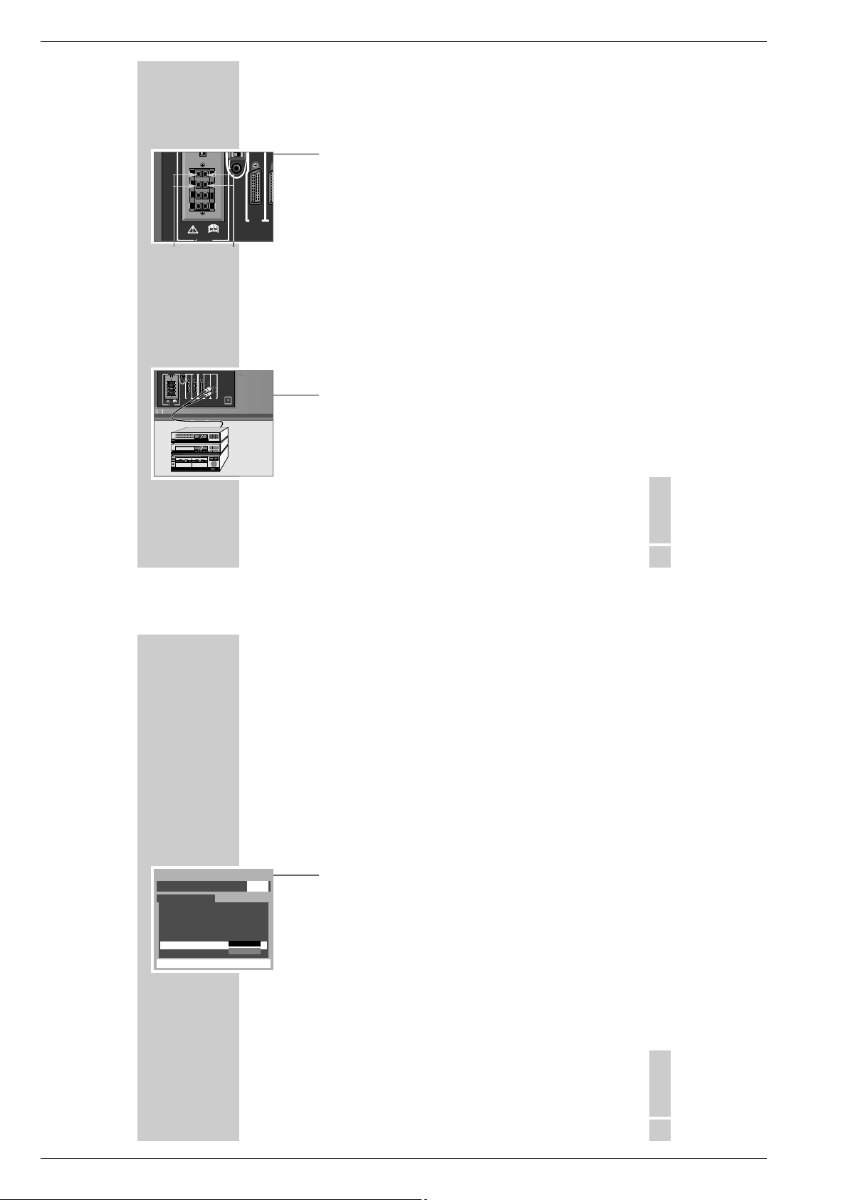
Sample connection of satellite receiver, video
recorder and decoder
Note:
If your video recorder is equipped with the Megalogic Plus system, the video
recorder must be connected to the Euro-AV socket »X(2)« of the TV set
using the Euro-AV cable supplied with the video recorder.
OPERATION WITH EXTERNAL EQUIPMENT
______
Video recorder
Satellite receiver
Decoder
MAIN(8Ω)
ƴ
EXT INT
(+)
R
(-)
(-)
R
(+)
SURROUND
(8Ω)
AUDIO
L
O
U
T
R
2 EXTERNAL / DEC. - AV 2
L
I
1 EXTERNAL / EURO - AV 1
N
R
R
~
220-240 V
50-60 Hz
AUDIO OUT
L
EURO AV VCREURO AV DECODEREURO AV TV
INPUT-SAT
950-2150 MHz
14/18 V 450 mA
28
WOOFER
(S-VIDEO)
(S-VIDEO)
EXT. INT.
(+)
L
(-)
(-)
L
(+)
(1)
(2)
X
X
(AUDIO/VIDEO) (VIDEO) (FIXED)
(AUDIO/VIDEO)
Manufactured under license from Dolby Laboratories. “Dolby”, “Pro Logic” and the
double-D symbol are trademarks of Dolby Laboratories. Confidential Unpublished
Works. ©1992-1997 Dolby Laboratories, Inc. All right reserved.
PAY-TV
38
COMPONENT
VIDEO INPUT
Y
PB/C
B
L
PR/C
AUDIO
R
R
(3)
(4)
X
SAT
TV R
GRUNDIG Service 1 - 21

Allgemeiner Teil / General Section ACCORO 102
ENGLISH
45
SPECIAL FUNCTIONS
__________________________________________________
Programming TV channels manually
This setting is only necessary if a new TV channel is added.
1
Call up the Dialog Center using the »Menu« button.
2
Select the »« menu using the »« or »« button.
3
Select »Manual Tune« using »« then press »«.
– The »MANUAL TUNE« menu appears.
4
Press »OK« to start the search function. »>>>« appears on the picture
screen.
The search stops as soon as a channel is found.
If the found channel is not the desired one, start the search again by
pressing »OK«.
5
Select »Programme no« using »« then enter the desired programme position number step by step using »
« or »«, or enter the number directly
using the »1...0« buttons.
6
In most cases, the station name is recognized automatically by the TV set. If
this is not the case, select the »Station« row using the »
« button then sel-
ect the desired name using »
« or »«.
7
Press »OK« to store the setting.
8
Press »Exit« to end the setting.
Note:
If the new channel number is known, you may enter it directly. In this case,
select under step
4
the »Channel« row, then enter the channel number step
by step using »
« or »«, or enter the number directly using the »1...0«
buttons.
MANUAL TUNE
&
ĵŁ
%$$
ĵŁ
ĵŁ
ĵŁ
: To store
:To exit
+
3
456
4:
78
46
SPECIAL FUNCTIONS
___________________________________________________________
Fine tuning
The TV set tunes automatically to optimum picture and sound quality.
In difficult reception conditions it may be necessary to manually fine tune to best
picture and sound quality.
1
Press the »Menu« button to call up the Dialog Center.
2
Select the »« menu using the »« or »« button.
3
Select the »Manual fine tuning« row using »« then press »«.
– The »Manual fine tuning« scale appears.
4
Use »« or »« to tune to best picture and sound quality.
5
Press »Exit« to end the setting.
Programme swap
Example: the programme on position 5 is to be swapped with position 2.
1
Press the »Menu« button to call up the Dialog Center.
2
Select the »« menu using the »« or »« button.
3
»Select the »Programme swap« row using »« then press »«.
– The»PROGRAMME SWAP« menu appears.
4
Select programme position 5 with »« then confirm with »OK«.
5
Select programme position 2 with »« or »« then confirm with »OK«.
The programme which has been on position 5 now is on position 2.
6
Press »Exit« to end the setting.
Manual fine tuning
––––––––––––––––●–––––––––––––––
PROGRAMME SWAP
ENTER : To select EXIT :To exit
Prog. StationļChannel
1 ARD 6
2 ZDF 34
3 BR-3 59
4 RTL 36
Ļ
1 - 22 GRUNDIG Service

ACCORO 102 Allgemeiner Teil / General Section
ENGLISH
47
SPECIAL FUNCTIONS
___________________________________________________________
Switching to blue picture screen
With this function the TV set switches to a blue screen if the picture is noisy
(poor aerial signal). The sound is muted. After about 20 minutes, the TV set
switches to standby.
1
Call up the Dialog Center using the »Menu« button then select the »S«
menu using the »
« or »« button.
2
Select »Blue screen« using the »« button (second menu page).
3
Use »« or »« to select » ON«.
4
Press »Exit« to end the setting.
FEATURE MENU
EXIT :To exit
0
ĵŁ
ĵŁ
2
Ł
OFF
ON
48
SPECIAL FUNCTIONS
___________________________________________________________
Adjusting the convergence
With your TV set the three basic colours red, green and blue are separately
projected onto the picture screen. The three colours must exactly match each
other. As a rule, this setting needs not to be changed. However, if the picture
should have unsharp borders or blurred colours, it is possible to correct the
convergence setting.
1
Call up the Dialog Center using the »Menu« button then select the »S«
menu using the »
« or »« button.
2
Select the »Convergence « row using »« (second menu page) then press
»
«. A cross and nine numbered rectangles appear on the picture screen.
3
Press the »red button«
4
Use »«, »«, »« and »« to move the red colour onto the white cross
in such a way that no shadows are visible.
5
Press the»blue button« and repeat the procedure for the blue colour.
6
Adjust the convergence of the picture borders by calling up the respective
rectangle using the »1...9« buttons, and then effecting the setting described
further up for the colours red and blue for each rectangle.
7
Press »Exit« to end the setting.
FEATURE MENU
EXIT :To exit
0
ĵŁ
ĵŁ
2
Ł
OFF
ON
GRUNDIG Service 1 - 23

Allgemeiner Teil / General Section ACCORO 102
Servicehinweise
1. Öffnen des Gerätes
–Vor dem Öffnen des Gerätes dieses vom Netz trennen.
–Sicherheitshinweise (siehe Sicherheit-Service-Manual, Material-
nummer 720108000000) beachten.
1.1 Rückwand
–5 Schrauben A, 3 Schrauben B und 2 Schrauben C herausdre-
hen (Fig. 1).
–Rückwand abnehmen.
1.2 Projektionsschirm
–Projektionsschirm gegen herunterfallen sichern.
–6 Schrauben D (Fig. 1) herausdrehen und Projektionsschirm
abnehmen.
1.3 Lautsprechergitter
–Lautsprechergitter gegen herunterfallen sichern.
–4 Schrauben E (Fig. 1) herausdrehen und Lautsprechergitter
abnehmen.
D
Service Instructions
1. Opening the Set
–Disconnect the set from the mains before opening it.
–Observe the safety hints (see Safety Service Manual, part number
720108000000).
1.1 Rear panel
–Undo the 5 screws A, 3 screws B and 2 screws C (Fig. 1).
–Remove the rear panel.
1.2 Projection screen
–Secure the projection screen against falling down.
–Undo the 6 screws D (Fig. 1) then remove the projection screen.
1.3 Loudspeaker grille
–Secure the loudspeaker grille against falling down.
–Undo the 4 screws E (Fig. 1) then remove the loudspeaker grille.
M
K
Fig. 2
B
E
C
E
A
Fig. 1 Fig. 3
2. Ausbauhinweise
2.1 Leitungsverlegung
Bevor Sie die Leitungen lösen ist die Leitungsverlegung zu den
einzelnen Baugruppen zu beachten.
Nach erfolgter Reparatur ist es notwendig, die Leitungsführung wieder
in den werkseitigen Zustand zu versetzen um evtl. spätere Ausfälle
oder Störungen zu vermeiden.
2.2 Chassis ausbauen
–3 Schrauben F (Fig. 2) herausdrehen.
–Chassis vorsichtig herausziehen.
–Gegebenenfalls Leitungen frei legen.
Servicestellung: siehe Fig. 3
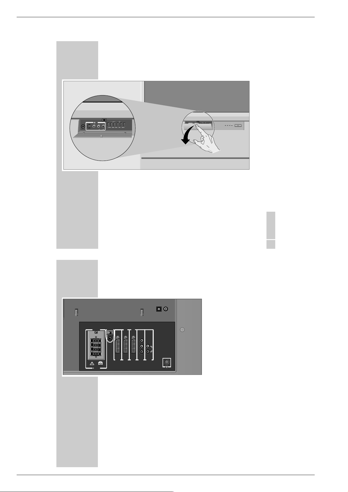
2.3 Buchsenplatte (Back AV Board) ausbauen
–Rastnasen im unteren Bereich der Buchsenabdeckung lösen:
Buchsenabdeckung im oberen Bereich vorsichtig nach innen drükken und unten herausziehen.
–Buchsenplatte mit Buchsenabdeckung nach oben herausziehen.
Montagehinweis:
–Buchsenplatte und Buchsenabdeckung vorsichtig im unteren Be-
reich so weit auseinander ziehen, dass die Steckverbindungen der
Buchsenplatte im Signal Board kontaktiert werden kann.
2. Disassembly Instructions
2.1 Wiring
Bevore disengaging the leads note the wiring to the individual
subassemblies.
When the repair is completed, the wiring must be re-established to its
factory state to prevent possible failures or distortions at a later date.
2.2 Removing the chassis
–Undo the 3 screws F (Fig. 2).
–Carefully pull out the chassis.
–If necessary disengage the leads.
Service position: see Fig. 3
2.3 Removing the sockets board (back AV board)
–Disengage the locking lugs in the bottom area of the sockets cover:
carefully press inwards the sockets cover in the top area then pull it
out downwards.
–Pull out upwards the sockets board along with the sockets cover.
Re-assembly:
–Carefully pull apart the sockets board and the sockets cover in the
lower area so that the plug connectors of the socket board can
engage into the contacts of the signal board.
–Lock in the bottom part of the sockets cover.
–Buchsenabdeckung unten einrasten.
F F
1 - 24 GRUNDIG Service

ACCORO 102 Allgemeiner Teil / General Section
2.4 Bildröhre (R, G, B) ausbauen
Achtung: Die Sechskantschrauben mit Feder (Fig. 4) dürfen nicht
gelöst werden da sonst Kühlflüssigkeit ausläuft.
–Bildrohrplatte abziehen.
–2 Schrauben G (Fig. 5) mit einem antimagnetischen Schrauben-
dreher lösen und SVM-Spule sowie Ablenkeinheit vom Bildrohrhals
entfernen.
–4 Schrauben H (Fig. 6) herausdrehen und die Linseneinheit
abnehmen. Linsen nicht mit den Fingern berühren.
–Anodenanschluss am Hochspannungsverteiler Z450 entgegen
dem Uhrzeigersinn drehen und abziehen.
–4 Schrauben I (Fig. 6) herausdrehen und Bildrohr herausnehmen.
Montagehinweis:
–Spezial-Silikon, Materialnummer 759880647200, an der Bildröhre
auftragen und neuen Anodenanschluss (Hochspannungs-Clip) anbringen (Fig. 7).
Hinweisaufdruck des Silikons zur Trocknung (ca. 24 Stunden)
beachten.
–Anoden-Kabelhalter J (Fig. 8) des alten Anodenanschlusses am
neuen Anodenanschluss anbringen.
Servicearbeiten nach Austausch der Bildröhre:
–Cutoff-Einstellung durchführen (S. 2-4, Abgleich Nr. 1)
–3 Schrauben K (Fig. 2) herausdrehen, Abdeckung abnehmen und
Fokus-Abgleich (S. 2-4, Abgleich Nr. 2) durchführen.
–2 Schrauben G (Fig. 5) mit einem antimagnetischen Schrauben-
dreher lösen und Ablenkung so einstellen, dass das Testbild mittig
und nicht verdreht ist. 2 Schrauben G (Fig. 5) wieder fest drehen.
–Mit den Geometrie-Einstellringen L (Fig. 5) die statische Konver-
genz einstellen.
–Konvergenz einstellen (S. 2-2, Punkt 6).
–Weiß-Abgleich durchführen (S. 2-4, Abgleich Nr. 3)
2.4 Removing the picture tube (R, G, B)
Attention: the hexagon-headed screws with spring (Fig. 4) must
not be undone as otherwise cooling liquid will leak.
–Pull off the picture tube panel.
–Undo the 2 screws G (Fig. 5) using an antimagnetic screw driver
then remove the SVM coil and the deflection unit from the picture
tube neck.
–Undo the 4 screws H (Fig. 6) then remove the lens unit. Do not
touch the lens with your fingers.
–Turn the anode connector on the high voltage distributor Z450
counterclockwise then pull it off.
–Undo the 4 screws I (Fig. 6) and remove the picture tube.
Re-assembly:
–Apply special silicon, material number 759880647200, to the picture
tube and fit the new anode connector (high voltage clip)
(Fig. 7).
Observe the printed note about drying (about 24 hours) on the
silicon.
–Fit the anode cable clip J (Fig. 8) of the old anode connector to the
new anode connector.
Service Works after the Replacement of the Picture Tube:
–Carry out the Cutoff alignment (p. 2-9, alignment no. 1)
–Undo the 3 screws K (Fig. 2), remove the cover, then carry out the
focus alignment (p. 2-9, alignment no. 2).
–Undo the 2 screws G (Fig. 5) with an antimagnetic screw driver then
adjust the deflection unit so that the test pattern is perfectly located
in the centre. Retighten the 2 screws G (Fig. 5).
–Use the geometry alignment rings L (Fig. 5) to adjust the static
convergence.
–Adjust the convergence (p. 2-7, Point 6).
–Carry out the white alignment (p. 2-9, alignment no. 3)
Fig. 4
Fig. 5
H
I
L
G
Fig. 6
J
2~5mm
15~25mm
Silicon
Fig. 7
GRUNDIG Service 1 - 25
Fig. 8

Allgemeiner Teil / General Section ACCORO 102
SCREEN VR
FOCUS VR
RG
B
Fig. 9
3. Kondenswasserableiter
Bei der Montage des Gerätes muss der Kondenswasserableiter
M
(Fig. 2) angebracht sein.
4. Pflege der Linsen und des Spiegels
Spiegel und Linsen dürfen nicht mit den Fingern berührt werden.
Staubbelag vorsichtig abblasen.
Flecken mit einem Reinigungstuch des Optiker-Fachhandels reinigen.
5. Hochspannung
Die Hochspannung an den Anoden der Bildröhren darf bei schwarzem
Bild eine Spannung von 33,8kV nicht übersteigen (Netzspannung
230V).
6. Durchführen von Messungen
Bei Messungen mit dem Oszilloskop an Halbleitern sollten Sie nur
Tastköpfe mit 10:1 - Teiler verwenden. Außerdem ist zu beachten,
dass nach vorheriger Messung mit AC-Kopplung der Koppelkondensator des Oszilloskops aufgeladen sein kann. Durch die Entladung
über das Messobjekt können Bauteile beschädigt werden.
7. Messwerte und Oszillogramme
Bei den in den Schaltplänen und Oszillogrammen angegebenen
Messwerten handelt es sich um Näherungswerte!
3. Condensation Water Drain
When the TV set is installed the condensation water drain M (Fig. 2)
must be fitted.
4. Care of the Lenses and of the Mirror
Do not touch the lenses and the mirror with your fingers.
Carefully blow off dust layers.
Remove stains using a special optician cleansing cloth.
5. High Voltage
The high voltage at the anodes of the picture tubes must not surpass
33.8kV with a black picture (230V mains voltage).
6. Carrying out Measurements
When making measurements on semi-conductors with an oscilloscope, ensure that the test probe is set to 10:1 dividing factor. If the
previous measurement was made on AC input, please note that the
coupling capacitor in the oscilloscope will be charged. Discharge via
the item being checked can damage the components.
7. Measured Values and Oscillograms
The measured values given in the circuit diagrams and oscillograms
are approximates!
1 - 26 GRUNDIG Service

ACCORO 102 Abgleich
SELFCHECK
2300xxxx
TIME : 123456
POWER : 00
BUS CONT : OK
BLOCK : UV V1 V2 V3
QV01
Softwarestand
Betriebsstunden
Schutzschaltung
Bus-Kontrolle
Eingangsquelle
Abgleich
1. Service-Betrieb
1.1 Service-Betrieb aktivieren
–Taste p drücken.
–Taste p nochmals drücken, gedrückt halten und am Gerät die
Taste MENU drücken.
–Auf dem Bildschirm erscheint die Bezeichnung des Abgleiches und
der Abgleichwert.
Abgleich
Einstellwert
1.2 Service-Betrieb beenden
–Bereitschaftstaste A drücken oder Gerät ausschalten.
1.3 Tastenfunktionen
– Fernbedientasten
1 R cutoff-Abgleich Anzeige "RCUT"
2 G cutoff-Abgleich Anzeige "GCUT"
3 B cutoff-Abgleich Anzeige "BCUT"
4 Grund-Kontrast Anzeige "SCNT"
5 Grund-Farbkontrast Anzeige "COLP" bei PAL
6 Farbeinstellung NTSC Anzeige "TNTC"
9 Selbstdiagnose (siehe Punkt 5)
e Testbilder PAL/NTSC (rot / grün / blau / Gitter / weiß, siehe
Punkt. 3)
ɾ
(gelb) Konvergenz-Abgleich (siehe Punkt 6)
CALL Initialisierung (siehe Punkt 2) / Zähler für Betriebsstunden und
Schutzschaltung löschen (siehe Punkt 5)
Info Bild abschalten für SCREEN-Abgleich
– Nahbedientasten
zɦ Service-Funktion wählen
Łĵ Abgleichwert ändern
MENU Abgleichmenu aus-/einblenden
RCUT 0410H
40H 10000000B
Anzeige "COLS" bei SECAM
Anzeige "COLC" bei NTSC
3. Testbilder
–Service-Betrieb aktivieren (siehe Punkt 1.1).
–Bei jedem Drücken der Taste e erscheinen nacheinander die
Testbilder Rot, Grün, Blau, Gitter, Weiß für PAL und dann für NTSC.
4. Basis-Einstellwerte (PAL-Breitwand-Zoom)
Anzeige Bezeichnung Referenzwert
RCUT R-cutoff (Schwarzwert) 40H
GCUT G-cutoff (Schwarzwert) 40H
BCUT B-cutoff (Schwarzwert) 40H
RDRV R-Verstärkung (Weißwert) 40H
BDRV B-Verstärkung (Weißwert) 40H
BRTC Grund-Helligkeit 80H
COLP Grund-Farbsättigung PAL 3DH
COLS Grund-Farbsättigung SECAM 3DH
SCNT Grund-Kontrast 08H
SBY SECAM B-Y 01H
SRY SECAM R-Y 07H
HPOS Horizontal-Position 67H
VPOS Vertikal-Position 09H
HIT Bildhöhe 3FH *
VLIN Vertikal-Bildlinearität 11H *
VSC Vertikal-Symmetrie 0BH
VPS Vertikal-Arbeitspunkt 1CH
WID Bildbreite 1EH
PARA Ost-West 11H
CNR Eckenkorrektur 01H
TRAP Trapez 20H
VFC Vertikal-Linearität (unten) 0FH
VCEN Vertikal-Zentrum 6AH
* Basiseinstellwerte für Bildformate
Bildformat HIT VLIN
Breitwand-Zoom 3FH 11H
Herkömmlich 4:3 3FH 11H
Super Live 4CH 0EH
Kino-Zoom 62H 11H
Kino-Zoom mit Untertitel 51H 11H
14:9 51H 11H
5. Selbstdiagnose
–Service-Betrieb aktivieren (siehe Punkt 1.1).
–Taste 9 drücken.
Auf dem Bildschirm erscheinen die Werte der Selbstdiagnose.
2. Initialisierung des QA02
Achtung: Bei dieser Service-Funktion werden alle kunden- und
servicespezifischen Software-Einstellungen gelöscht.
Sollten im Servicefall die eingestellten Werte der Service-Funktionen
aufrufbar (siehe Punkt 4) sein, ist es ratsam, diese zu notieren, um sie
nach Austausch bzw. Initialisierung des QA02 wieder einstellen zu
können.
Der QA02 ist nach dem Wechsel zu intitialisieren.
–Service-Betrieb aktivieren (siehe Punkt 1.1)
–Taste CALL auf der Fernbedienung drücken, gedrückt halten und am
Gerät die Taste ɦ drücken.
Das Bild wird schwarz und das Gerät schaltet kurzzeitig in den
Standby-Betrieb.
–Service-Betrieb aktivieren (siehe Punkt 1.1)
–Taste CALL auf der Fernbedienung drücken, gedrückt halten und am
Gerät die Taste MENU drücken.
Achtung: In dieser Betriebsart nur folgende Einstellungen vorneh-
men. Ansonsten sind die Gerätefunktionen nicht gewährleistet.
–Mit der Taste z die Service-Funktion"OPT1" anwählen und mit
den Tasten Łĵ den Wert "7EH" einstellen.
–Mit der Taste z die Service-Funktion"OPT0" anwählen und mit
den Tasten Łĵ den Wert "B0H" einstellen.
–Bildeinstellungen prüfen und korrigieren (siehe Punkte 6 und 7,
Abgleich Nr. 1, 3…6).
GRUNDIG Service 2 - 1
–Taste 9 nochmals drücken.
Auf dem Bildschirm erscheinen die Werte des EPG/TEXT.
SELFCHECK
EPG/TEXT
QF01 xxx QF10 xxx
QF02 xxx QF03 xxx
QF04 xxx QF05 xxx

Abgleich ACCORO 102
Softwarestand
Dies ist Softwarestand des µP QA01.
Betriebsstunden und Schutzschaltung
–Der Betriebsstundenzähler zeigt die Betriebsstunden des Gerätes.
–Der Zähler für die Schutzschaltung gibt an, wie oft diese bereits
angesprochen hat.
Die Betriebsstunden- und Schutzschaltungszähler sind löschbar:
–Taste CALL auf der Fernbedienung drücken, gedrückt halten und am
Gerät die Taste z drücken. Anschließend schaltet das Gerät kurz-
zeitig in den Standby-Betrieb.
Bus-Kontrolle
Im Normalfall wird "OK" (grün) angezeigt.
Sollte ein Fehler aufgetreten sein, wird das Bauteil "Qxxx" rot angezeigt, mit dem keine Kommunikation möglich war.
Eingangsquelle
–Die Eingangsquelle gibt die aktive Eingangsquelle (UV = Tuner;
V1 = Video 1; V2 = Video 2; V3 = Video 3) an. Steht dort ein
brauchbares Signal an, dann ist die Anzeige der Eingangsquelle
"grün", ansonsten ist diese "rot". Ein Fehler ist an der Eingangseite
des QV01 zu suchen.
–Die grüne Anzeige QV01 gibt an, dass das Signal an der Ausgang-
seite in Ordnung ist. Bei einer roten Anzeige QV01 sind der QV01
und die folgenden Schaltungen zu prüfen.
EPG/TEXT
Pos. Bezeichnung xxx Beschreibung
QF01 MEGATEXT ERR MEGATEXT-Fehler (SDA5275)
QF10 DRAM 00 kein DRAM
QF02 SUB-MICON 02 C161RI Version BB-Schritt
QF03 PROGRAMM ERR ROM-Fehler
FLASH-ROM xxyy Softwarestand xx.yy
QF04 DATA ERR FLASH-ROM-Fehler
FLASH ROM 00 kein FLASH-ROM
QF05 EEPROM ERR EEPROM-Fehler
00 undefiniert
20 MEGATEXT – SDA5275-3P C02-22
18 8Mbit DRAM (2k-refresh-Typ 16Mbit DRAM)
20 16Mbit DRAM (4k-refresh-Typ 16Mbit DRAM)
04 C161RI Version AA-Schritt
A4 AM29F040 (AMD, 4Mbit)
MBM29F040C (Fujitsu, 4Mbit)
MX29F040 (Macronix, 4Mbit)
FF unbekanntes 4Mbit FLASH-ROM
00 kein EEPROM
12 8kbit EEPROM
6. Konvergenz
–Service-Betrieb aktivieren (siehe Punkt 1.1).
–Taste ɾ
Auf dem Bildschirm erscheint das Konvergenz-Testbild.
(gelb) drücken.
6.1 Konvergenz-Tastenbelegung der Fernbedienung
3 Wählt einzustellenden Strahl aus(R = rot / G = grün / B = blau)
5 Aktiviert / deaktiviert einzustellenden Strahl
2 auf für Einstellbereich und Strahlablenkung
4
6 links 4 / rechts 6 für Einstellbereich und Strahlablenkung
8 ab für Einstellbereich und Strahlablenkung
ї
(rot) Farbe rot aus-/einblenden
Ƒ
(grün) Farbe grün aus-/einblenden
ƴ
(blau) Farbe blau aus-/einblenden
ɾ
(gelb) Konvergenz-Abgleich verlassen / aufrufen
6.2 Konvergenz einstellen ohne Konvergenz-Menü
Für die Einstellung der PAL-Konvergenz ist ein PAL-Testbild einzuspeisen und für NTSC-Konvergenz ein NTSC-Testbild.
a
. Service-Betrieb aktivieren (siehe Punkt 1.1).
b
. Ablenkeinstellungen und Geometrieeinstellungen prüfen und even-
tuell korrigieren (Basiswerte – siehe Punkt 4, Abgleichvorschriften
– Punkt 7, Abgleich Nr. 4…7).
c
. Bildformat mit der Taste q wählen.
d
. Taste ɾ
(gelb) drücken. Anschließend erscheint das Konvergenz-
Testbild.
e
. einzustellenden Bereich mit den Tasten 2 (oben), 4 (links),
6 (rechts), 8 (unten) auswählen und mit der Taste 5 aktivieren.
f
. einzustellenden Strahl (rot / grün / blau) mit der Taste 3 auswählen.
g
. gegebenenfalls einzelne Farben mit den Tasten ї (rot), Ƒ(grün),
ƴ (blau) aus- bzw. einblenden.
h
. mit den Tasten 2 (oben), 4 (links), 6 (rechts), 8 (unten) entspre-
chend der Mustertestbilder (Punkt 6.3) einstellen und die Farben rot,
grün und blau zur Deckung bringen (Punkte
i
. Zum Beenden der Konvergenz-Einstellung die Taste ɾ
mal drücken.
Hinweis:
–Für die komplette Konvergenzeinstellung eines Bildformates sind
die Punkte e bis h zu wiederholen.
–Die Konvergenz ist für alle möglichen Bildformate (Punkt 6.3)
c
einzustellen (Punkte
bis h wiederholen).
6.3 Konvergenz einstellen über das Konvergenz-Menü
a
. Für die Einstellung der PAL-Konvergenz ist ein PAL-Testbild einzu-
speisen und für NTSC-Konvergenz ein NTSC-Testbild.
b
. Service-Betrieb aktivieren (siehe Punkt 1.1).
c
. Ablenkeinstellungen und Geometrieeinstellungen prüfen und even-
tuell korrigieren (Basiswerte – siehe Punkt 4, Abgleichvorschriften
– Punkt 7, Abgleich Nr. 4…7).
d
. Tasten F und 7 der Service-Fernbedienung (Materialnummer
759880647300) gleichzeitig drücken.
Anschließend erscheint das Konvergenzmenü für die PAL- oder
NTSC-Konvergenzeinstellung:
–PAL-Konvergenzmenü
Conver Adjust Menu
1 Adjust PAL Wide
2 PAL Wide to Others
3 Adjust PAL S.Live
4 Adjust PAL Cinema
5 Adjust PAL S.title
6 PAL to NTSC(Wide)
7 PAL to NTSC(ALL)
f
bis h wiederholen).
(gelb) zwei-
X: 1
Y: 1
C: R
S: 01
Wide
Das blinkende Rechteck gibt den Konvergenz-Einstellbereich an.
X = X-Koordinate des Konvergenz-Einstellbereiches
Y = Y-Koordinate des Konvergenz-Einstellbereiches
–NTSC-Konvergenzmenü
Conver Adjust Menu
8 Adjust NTSC Wide
9 NTSC Wide to Others
10 Adjust NTSC S.Live
11 Adjust NTSC Cinema
12 Adjust NTSC S.title
C = aktivierter einstellbarer Strahl (R = rot / G = grün / B = blau)
S = aktives Menu
–Taste ɾ
(gelb) drücken. Die Bildeinstellungen (Höhe, Breite und
Geometrie) sind einstellbar.
Taste ɾ
Testbildes.
(gelb) nochmals drücken zum Beenden des Konvergenz-
Die weiteren Einstellungen sind mit dem Tele Pilot 130 C
möglich.
e
. Taste s drücken. Anschließend erscheint das Konvergenz-Test-
bild.
2 - 2 GRUNDIG Service

ACCORO 102 Abgleich
272
240
144
48
0
48
144
240
272
[mm]
0
76
76
228
380
432.5
228
380
432.5
f
. einzustellenden Bereich mit den Tasten 2 (oben), 4 (links),
6 (rechts), 8 (unten) auswählen und mit der Taste 5 aktivieren.
g
. einzustellenden Strahl (rot / grün / blau) mit der Taste 3 auswählen.
h
. gegebenenfalls einzelne Farben mit den Tasten ї(rot), Ƒ(grün),
6.3.4 Bildformat Kino-Zoom mit Untertitel (PAL Subtitle)
Hinweis: Nach Verlassen dieser Service-Funktion ist das Bild um ca.
13mm nach oben verschoben.
ƴ (blau) aus- bzw. einblenden.
i
. mit den Tasten 2 (oben), 4 (links), 6 (rechts), 8 (unten) entspre-
chend der Mustertestbilder (Punkt 6.3) einstellen und die Farben rot,
grün und blau zur Deckung bringen (Punkte g bis i wiederholen).
j
. Taste s drücken. Anschließend erscheint das Konvergenzmenü.
k
. Mit den Tasten AS
Taste s bestätigen. Die eingestellten Werte des
werden auf die Betriebsarten
S.title
l
übertragen.
. Mit den Tasten AS die Betriebsarten
und
PAL S.title
Gegebenenfalls sind die Konvergenz-Einstellungen zu korrigieren
(Punkte f bis j).
m
.Mit den Tasten AS
Taste s bestätigen. Die eingestellten Werte der PAL-Betriebsarten
werden auf NTSC-Betriebsarten übertragen.
n
. Zum Verlassen des Konvergenz-Menüs die Tasten F und 7 der
Service-Fernbedienung (Materialnummer 759880647300) gleichzeitig drücken.
o
. NTSC-Testbild einspeisen und ab Punkt c beginnen.
6.3 Bildformate
6.3.1 Bildformat 4:3 / Breitwand-Zoom (PAL Wide)
PAL Wide to Others
anwählen und mit der
Adjust PAL Wide
PAL S.Live, PAL Cinema
PAL S.Live, PAL Cinema
anwählen und mit der Taste s bestätigen.
PAL to NTSC(ALL)
anwählen und mit der
235
207.5
124.5
41.5
0
41.5
124.5
und
PAL
6.3.5 Bildformat 4:3 / Breitwand-Zoom (NTSC Wide)
0
432.5
380
228
76
76
228
380
6.3.6 Bildformat Super Live (NTSC Super Wide)
231
198
99
0
99
198
231
[mm]
432.5
0
432.5
380
228
76
76
228
6.3.2 Bildformat Super Live (PAL Super Wide)
428
372
218.5
72.5
0
72.5
218.5
6.3.3 Bildformat Kino-Zoom (PAL Cinema)
76
228
432.5
380
228
0
76
207.5
235
[mm]
380
432.5
249
220
130.5
40
0 (pattern center)
49.5
136.5
221
249
[mm]
372
428
262.5
227.5
157.5
52.5
0
52.5
157.5
227.5
262.5
380
432.5
[mm]
-5 (screen
center)
428
372
218.5
72.5
0
72.5
218.5
6.3.7 Bildformat Kino-Zoom (NTSC Cinema)
0
432.5
380
228
76
76
228
372
380
428
432.5
249
213
105
0 (pattern center)
-5 (screen
center)
112
216
249
[mm]
287
246
123
0
123
246
287
[mm]
GRUNDIG Service 2 - 3

Abgleich ACCORO 102
6.3.8 Bildformat Kino-Zoom mit Untertitel (NTSC Subtitle)
Hinweis: Nach Verlassen dieser Service-Funktion ist das Bild um ca.
13mm nach oben verschoben.
266
228
114
0
114
228
432.5
380
228
0
76
76
228
380
266
[mm]
432.5
7. Abgleichvorschriften
Messgeräte / Messmittel: Voltmeter, Tastköpfe 10:1, Farbgenerator, Service-Fernbedienung
Servicearbeiten nach Austausch …
… des QA02: Abgleich Nr. 1, 3…7, Konvergenz (S. 2-2, Punkt 6)
… eine der Bildröhren (R, G, B): Abgleich Nr. 1…3, 5…7, Konvergenz (S. 2-2, Punkt 6)
… des Fokusblocks: Abgleich Nr. 1, 2
… der ablenkbeeinflussenden Komponenten: Abgleich Nr. 4…7, Konvergenz (S. 2-2, Punkt 6)
Abgleich Vorbereitung Abgleichvorgang
1. Cutoff
SCREEN R, G, B
RCUT
GCUT
BCUT
–Graustufentestbild einspeisen.
–Kontrast: Maximum
–Hellgikeit und Farbe: Mittelstellung
–Taste p drücken.
–Taste p nochmals drücken, gedrückt halten und am
Gerät die Taste MENU drücken.
–Mit den Nahbedientasten zɦ die Service-Funktionen
RCUT, GCUT und BCUT anwählen und jeweils mit den
Nahbedientasten Łĵden Wert 40H einstellen.
–Helligkeit mit den Schirmgitterreglern (SCREEN) R, G
und B am Fokusblock (S. 1-26, Fig. 9) so einstellen, bis
jeweils der Strahl gerade wieder unsichtbar ist.
–Mit den Nahbedientasten zɦ die Service-Funktionen
RCUT, GCUT und BCUT anwählen und jeweils mit den
Nahbedientasten Łĵso einstellen, dass der schwarze
Bereich unbunt ist.
–Bei Bedarf den Service-Betrieb beenden durch Drücken
der Bereitschaftstaste A oder Ausschalten des Gerätes.
–Taste Info drücken (das Bild wird dunkel geschaltet).
2. RGB-Fokus
Linseneinheiten
FOCUS R, G, B
Hinweis: Der Fokusabgleich ist bei betriebswarmen Gerät
durchzuführen (nach min. 30 Minuten, besser noch nach 2
bis 3 Stunden).
–Taste p drücken.
–Taste p nochmals drücken, gedrückt halten und am
Gerät die Taste MENU drücken.
–Taste e so oft drücken bis ein Gitter-Testbild sichtbar ist.
–Nichtbenötigte Strahleinheiten abdecken (z.B: zur Ein-
stellung der roten Strahleinheit sind die grüne und blaue
abzudecken).
a) Flügelmutter (siehe Abbildung) der
einzustellenden Strahleinheit (z.B. rot)
lösen.
Linseneinheit so verdrehen, dass die
Schärfe gleichmäßig verteilt ist.
Flügelmutter wieder fest schrauben.
b) Mit dem Fokusregler (z.B. R) am Fokusblock (S. 1-26,
Fig. 9) Bildmitte am schärfsten einstellen.
c) Gegebenenfalls die Schritte a) und b) wiederholen.
d) Bei Bedarf den Service-Betrieb beenden durch Drücken
der Bereitschaftstaste A oder Ausschalten des Gerätes.
3. Weißabgleich
RDRV
BDRV
4. Vertikale Mittenspannung
VCEN
–Graustufentestbild einspeisen.
–Voltmeter
–Taste p drücken.
–Taste p nochmals drücken, gedrückt halten und am
Gerät die Taste MENU drücken.
–Voltmeter zwischen TP-V und TP-G (GND) anschließen.
–Weißtestbild einspeisen.
–Kontrast: Maximum
–Helligkeit und Farbe: Mittelstellung
–Taste p drücken.
–Mit den Nahbedientasten zɦ die Service-Funktionen
RDRV und BDRV anwählen und jeweils mit den
Nahbedientasten Łĵdas Bild unbunt (weiß) einstellen.
–Bei Bedarf den Service-Betrieb beenden durch Drücken
der Bereitschaftstaste A oder Ausschalten des Gerätes.
–Mit den Nahbedientasten zɦ die Service-Funktionen
VCEN anwählen und mit den Nahbedientasten Łĵdie
Spannung auf 30mV ±10mV einstellen.
–Bei Bedarf den Service-Betrieb beenden durch Drücken
der Bereitschaftstaste A oder Ausschalten des Gerätes.
–Taste p nochmals drücken, gedrückt halten und am
Gerät die Taste MENU drücken.
5. Bildbreite
WID
–Taste p drücken.
–Taste p nochmals drücken, gedrückt halten und am
Gerät die Taste MENU drücken.
–Taste e so oft drücken bis ein Gitter-Testbild sichtbar ist.
–Mit den Nahbedientasten zɦ die Service-Funktion WID
anwählen.
–Mit den Nahbedientasten Łĵdie Bildbreite so einstellen,
dass das Bild am linken und rechten Rand gerade verzerrt
ist bzw. sichtbar wird.
–Anschließend die Nahbedientaste Ł 13 mal drücken.
–Bei Bedarf den Service-Betrieb beenden durch Drücken
der Bereitschaftstaste A oder Ausschalten des Gerätes.
2 - 4 GRUNDIG Service

ACCORO 102 Abgleich
Abgleich Vorbereitung Abgleichvorgang
6. Bildhöhe
HIT
–Taste p drücken.
–Taste p nochmals drücken, gedrückt halten und am
Gerät die Taste MENU drücken.
–Taste e so oft drücken, bis das Gitter-Testbild sichtbar
ist.
–Mit den Nahbedientasten zɦ die Service-Funktion HIT
anwählen.
Der folgende Abgleichvorgang ist jeweils für die Bildformate
Breitwand-Zoom, Super Live, Kino-Zoom und Kino-Zoom
mit Untertitel auszuführen. Mit der Betriebsart BreitwandZoom ist zu beginnen.
–Bildformat mit der Taste q wählen.
–Mit den Nahbedientasten Łĵdie Bildhöhe so einstellen,
dass der obere Testbildrand sichtbar wird.
– Ausgehend vom sichtbaren Testbildrand die Nahbedien-
taste Ł entsprechend der Betriebsart drücken:
11 mal – Breitwand-Zoom
13 mal – Super Live
21 mal – Kino-Zoom
17 mal – Kino-Zoom mit Untertitel
–Bildformate kontrollieren und gegebenenfalls anpassen:
–entsprechend der Konvergenz-Testbilder (Punkt 6.3)
Aufruf: Taste ɾ
(gelb) zweimal drücken.
Bildformat durch Drücken der Taste q wählen.
–oder mit Hilfe des FUBK-Testbildes
FUBK-Testbild einspeisen und Taste e so oft drücken
bis dieses sichtbar ist.
Bildformat durch Drücken der Taste q wählen.
–Bei Bedarf den Service-Betrieb beenden durch Drücken
der Bereitschaftstaste A oder Ausschalten des Gerätes.
7. Geometrie
HPOS, VPOS
VLIN, VSC, VPS,
VFC, TRAP
PARA, CNR
–Geometrietestbild einspeisen.
–Taste p drücken.
–Taste p nochmals drücken, gedrückt halten und am
Gerät die Taste MENU drücken.
Der folgende Abgleichvorgang ist jeweils für die Bildformate
Breitwand-Zoom, Super Live, Kino-Zoom und Kino-Zoom
mit Untertitel auszuführen (siehe Bildformate Punkt 6.3). Mit
der Betriebsart Breitwand-Zoom ist zu beginnen.
–Bildformat durch Drücken der Taste q wählen.
–Mit den Nahbedientasten zɦ die Service-Funktion an-
wählen und mit den Nahbedientasten Łĵeinstellen:
–Mit HPOS die horizontale Bildmitte und mit VPOS die
vertikale Bildmitte einstellen.
–Mit VPS den richtigen Arbeitspunkt (beste Bild-
darstellung) wählen.
–Mit VLIN die vertikale Bildliniarität einstellen.
–Mit VSC die vertikale Symmetrie einstellen.
–Mit VFC die vertikale Linearität im unteren Bildbereich
einstellen.
–Mit TRAP die Trapezverzerrungen korrigieren.
–Mit PARA die OST-WEST-Korrektur durchführen.
–Mit CNR die vertikale Korrektur in den Ecken durchfüh-
ren.
–Bildformate entsprechend der Konvergenz-Testbilder
(Punkt 6.3) kontrollieren und gegebenenfalls anpassen:
–Aufruf: Taste ɾ
(gelb) zweimal drücken.
–Bildformat durch Drücken der Taste q wählen.
–Bei Bedarf den Service-Betrieb beenden durch Drücken
der Bereitschaftstaste A oder Ausschalten des Gerätes.
GRUNDIG Service 2 - 5

Alignment ACCORO 102
Alignment
1. Service Mode
1.1 Activating the service mode
–Press the p button.
–Press the p button again and keep it pressed while pressing the
MENU button on the set.
–On the picture screen appear the alignment name and the alignment
value.
Alignment Name
Alignment Value
1.2 Ending the service mode
–Press the standby button A or switch the set off.
1.3 Button functions
– Remote control buttons
1 R cutoff alignment Indication: "RCUT"
2 G cutoff alignment Indication: "GCUT"
3 B cutoff alignment Indication: "BCUT"
4 Basic contrast Indication: "SCNT"
5 Basic colour contrast Indication: "COLP" with PAL
6 NTSC colour adjustment Indication: "TNTC"
9 Selfcheck (see point 5)
e Test patterns PAL/NTSC (red / green/ blue/ raster/ white, see
Point 3).
ɾ
(yell.) Convergence alignment (see Point 6).
CALL Initialisiation (see Point 2) / clear counter for service hours and
overload protection circuit (see point 5).
Info Switch off pattern for SCREEN alignment.
– Direct control buttons (on the set)
zɦ Select service function.
Łĵ Change setting.
MENU Display/exit alignment menu.
RCUT 0410H
40H 10000000B
Indication: "COLS" with SECAM
Indication: "COLC" with NTSC
3. Test Patterns
–Activate the service mode (see Point 1.1).
–After every pressure on the e button appear one after the other the
test patterns red, green, blue, raster, white for PAL, and then for
NTSC.
4. Basic Settings (PAL wide-screen zoom)
Display Name Refer. value
RCUT R-cutoff (black level) 40H
GCUT G-cutoff (black level) 40H
BCUT B-cutoff (black levelt) 40H
RDRV R-amplification (white level) 40H
BDRV B-amplification (white level) 40H
BRTC Basic brightness 80H
COLP Basic colour saturation PAL 3DH
COLS Basic colour saturation SECAM 3DH
SCNT Basic contrast 08H
SBY SECAM B-Y 01H
SRY SECAM R-Y 07H
HPOS Horizontal position 67H
VPOS Vertical position 09H
HIT Picture height 3FH *
VLIN Vertical linearity 11H *
VSC Vertical symmetry 0BH
VPS Vertical operating point 1CH
WID Picture width 1EH
PARA East-West 11H
CNR Corner correction 01H
TRAP Trapezoid 20H
VFC Vertical linearity (bottom) 0FH
VCEN Vertical centre 6AH
* Basic settings for picture formats
Picture format HIT VLIN
Wide-screen zoom 3FH 11H
Conventional 4:3 3FH 11H
Super live 4CH 0EH
Cinema zoom 62H 11H
Cinema zoom with subtitles 51H 11H
14:9 51H 11H
5. Selfcheck
–Activate the service mode (see Point 1.1).
–Press the 9 button.
The selfcheck settings appear on the picture screen.
2. Initialization of the QA02
Attention: With this service function, all customer- and servicespecific software settings are cleared.
If the settings of the service functions should be displayable in the case
of service (see Point 4), it is recommended to note down these settings
in order to recover them after the replacement or the initialization of the
Software version
Operating hours
Overload-protection
Bus check
Input source
SELFCHECK
2300xxxx
TIME : 123456
POWER : 00
BUS CONT : OK
BLOCK : UV V1 V2 V3
QV01
QA02.
The QA02 is to be initialized after replacement.
–Activate the service mode (see Point 1.1)
–Press the CALL button on the remote control, hold it down and press
the ɦ button on the set.
The screen turns black and the set switches temporarily to standby.
–Press the 9 button again.
The EPG/TEXT settings appear on the picture screen.
–Activate the service mode (see Point 1.1)
–Press the CALL button on the remote control, hold it down and press
the MENU button on the set.
Attention: In this mode, carry out only the following settings,
otherwise the correct function of the set is not guaranteed.
–Use the z button to select the "OPT1" service function then use the
Łĵ buttons to set the "7EH" value.
SELFCHECK
EPG/TEXT
QF01 xxx QF10 xxx
QF02 xxx QF03 xxx
QF04 xxx QF05 xxx
–Use the z button to select the "OPT0" service function then use the
Łĵ buttons to set the "B0H" value.
–Check and correct the picture settings (see Points 6 and 7, alignment
no. 1, 3…6).
2 - 6 GRUNDIG Service

ACCORO 102 Alignment
Software version
This is the software version of the µP QA01.
Operating hours and overload-protection circuit
–The operating hours counter indicates the operating hours of the set.
–The counter for the overload-protection circuit indicates how often
this has responded.
The operting hours and overload-protection circuit counters can be
cleared.
–Press and hold down the CALL button on the remote control while
pressing the z button on the set. The set switches temporarily to
standby.
Bus check
Normally "OK" (green) is displayed.
If a failure should have been occurred, the component "Qxxx" with
which no communication was possible is displayed in red.
Input source
–The input source indicates the active input source (UV = Tuner;
V1 = Video 1; V2 = Video 2; V3 = Video 3). If a useful signal is
present there, the input source indication is "green", otherwise it is
"red". A failure is to be searched at the input side of the QV01.
–The green QV01 indication means that the signal at the output side
is ok. In the case of a red QV01 indication, the QV01 and the
following circuits are to be checked.
EPG/TEXT
Pos. Name xxx Description
QF01 MEGATEXT ERR MEGATEXT error (SDA5275)
00 undefined
20 MEGATEXT – SDA5275-3P C02-22
QF10 DRAM 00 no DRAM
18 8Mbit DRAM (2k refresh-type 16Mbit DRAM)
20 16Mbit DRAM (4k refresh-type 16Mbit DRAM)
QF02 SUB-MICON 02 C161RI Version BB-step
04 C161RI Version AA-step
QF03 PROGRAMM ERR ROM error
FLASH-ROM xxyy Software version xx.yy
QF04 DATA ERR FLASH-ROM error
FLASH ROM 00 no FLASH-ROM
A4 AM29F040 (AMD, 4Mbit)
MBM29F040C (Fujitsu, 4Mbit)
MX29F040 (Macronix, 4Mbit)
FF unknown 4Mbit FLASH-ROM
QF05 EEPROM ERR EEPROM error
00 no EEPROM
12 8kbit EEPROM
6.1 Convergence button assignment of the remote control
3 Selects the adjustable beam (R = red / G = green / B = blue)
5 Activates/deactivates the adjustable beam.
2 Up for setting area and beam deflection
4
6 Left 4 / right 6 for setting area and beam deflection.
8 Down for setting area and beam deflection.
ї
(red) Display/suppress the red colour
Ƒ
(green) Display/suppress the green colour
ƴ
(blue) Display/suppress the blue colour
ɾ
(yellow) Exit/call up the convergence alignment.
6.2 Convergence alignment without convergence menu
For the PAL convergence alignment a PAL test pattern must be
injected, for the NTSC convergence alignment an NTSC test pattern.
a
. Activate the service mode (see point 1.1).
b
. Check the deflection and geometry settings and correct if necessary
(basic values – see Point 4, Alignment Instructions – Point 7,
alignment no. 4…7).
c
. Select the picture format using the q button.
d
. Press the ɾ
e
. Select the area to be adjusted using the buttons 2 (top), 4 (left),
(yellow) button. The convergence test pattern appears.
6 (right), 8 (bottom) then press the 5 button to activate it.
f
. Select the adjustable beam (red/green/blue) using the 3 button.
g
. If necessary display or suppress individual colours using the ї (red),
Ƒ (green), ƴ (blue) buttons.
h
. Use the buttons 2 (up), 4 (left), 6 (right), 8 (down) to adjust
according to the test patterns (Point 6.3) and bring the red, green and
blue colours to coincidence (repeat the steps
i
. Press the ɾ
(yellow) button twice to end the convergence alignment.
Note:
–For a complete convergence alignment for one picture format, it is
necessary to repeat the steps e to h.
–The convergence must be adjusted for every picture format (Point
c
6.3) (repeat the Points
to h ).
6.3 Convergence alignment via the convergence menu
a
. For the PAL convergence alignment a PAL test pattern must be
injected, for the NTSC convergence alignment an NTSC test
pattern.
b
. Activate the service mode (see point 1.1).
c
. Check the deflection and geometry settings and correct if necessary
(basic values – see Point 4, Alignment Instructions – Point 7,
alignment no. 4…7).
d
. Press the F and 7 button on the service remote control (material
number 759880647300) at the same time.
The PAL or NTSC convergence alignment menu appears.
–PAL convergence menu
f
to h).
6. Convergence
–Activate the service mode (see point 1.1).
–Press the ɾ
The convergence test pattern appears on the picture screen.
The flashing rectangle indicates the convergence setting area.
X = X-coordinate of the convergence setting area.
Y = Y-coordinate of the convergence setting area.
C = activated adjustable beam (R = red / G = green / B = blue)
S = activated menu.
–Press the ɾ
geometry) can be changed.
Press the ɾ
(yellow) button.
X: 1
Y: 1
C: R
S: 01
Wide
(yellow) button. The picture settings (height, width and
(yellow) button again to exit the convergence test pattern.
Conver Adjust Menu
1 Adjust PAL Wide
2 PAL Wide to Others
3 Adjust PAL S.Live
4 Adjust PAL Cinema
5 Adjust PAL S.title
6 PAL to NTSC(Wide)
7 PAL to NTSC(ALL)
–NTSC convergence menu
Conver Adjust Menu
8 Adjust NTSC Wide
9 NTSC Wide to Others
10 Adjust NTSC S.Live
11 Adjust NTSC Cinema
12 Adjust NTSC S.title
The further settings can be carried out with the Tele Pilot 130 C.
e
. Press the s button. The convergence test pattern appears.
GRUNDIG Service 2 - 7

Alignment ACCORO 102
f
. Select the area to be adjusted using the buttons 2 (top), 4 (left),
6 (right), 8 (bottom) then press the 5 button to activate it.
g
. Select the adjustable beam (red/green/blue) using the 3 button.
h
. If necessary display or suppress individual colours using the ї(red),
Ƒ (green), ƴ (blue) buttons.
i
. Use the buttons 2 (up), 4 (left), 6 (right), 8 (down) to adjust
6.3.4 Picture format Cinema Zoom with subtitles (PAL Subtitle)
Note: after exiting this service function the picture is shifted about
13mm to the top.
272
240
according to the test patterns (Point 6.3) and bring the red, green and
380
144
48
0
48
144
240
272
[mm]
432.5
231
198
blue colours to coincidence (repeat the steps g to i).
j
. Press the s button. The convergence menu appears.
k
. Use the AS buttons to select
button to confirm. The
the
PAL S.Live, PAL Cinema
l
. Use the AS buttons to select the
S.title
modes then press s to confirm.
PAL Wide to Others
Adjust PAL Wide
and
PAL S.title
PAL S.Live, PAL Cinema
settings are transferred to
then press the s
modes.
and
PAL
If necessary correct the convergence settings (Points f to j).
m
. Use the AS buttons to select
PAL to NTSC(ALL)
then press the s
button to confirm. The PAL mode settings are transferred to the
NTSC modes.
n
. To exit the convergence menu press the F and 7 buttons on the
service remote control (material number 759880647300) at the
same time.
o
. Feed in an NTSC test pattern and begin with Point c.
6.3 Picture formats
0
432.5
380
228
76
76
228
6.3.5 Picture format 4:3 / Wide-screen Zoom (NTSC Wide)
6.3.1 Picture format 4:3 / Wide-screen Zoom (PAL Wide)
380
99
0
99
198
231
[mm]
432.5
249
213
432.5
380
228
235
207.5
124.5
41.5
0
41.5
0
124.5
207.5
0
76
76
228
380
235
[mm]
432.5
380
432.5
6.3.6 Picture format Super Live (NTSC Super Wide)
228
76
76
228
6.3.2 Picture format Super Live (PAL Super Wide)
105
0 (pattern center)
112
216
249
[mm]
372
428
287
246
-5 (screen
center)
428
372
218.5
72.5
249
220
130.5
40
0 (pattern center)
-5 (screen
49.5
center)
136.5
221
0
72.5
218.5
372
428
249
[mm]
372
428
218.5
6.3.7 Picture format Cinema Zoom (NTSC Cinema)
72.5
0
72.5
218.5
6.3.3 Picture format Cinema Zoom (PAL Cinema)
380
123
0
123
246
287
[mm]
432.5
432.5
380
228
262.5
227.5
157.5
52.5
0
52.5
0
157.5
227.5
262.5
0
76
76
228
380
[mm]
432.5
432.5
380
228
76
76
228
2 - 8 GRUNDIG Service

ACCORO 102 Alignment
6.3.8 Picture format Cinema Zoom with subtitles (NTSC Subtitle)
Note: after exiting this service function the picture is shifted about
13mm to the top.
266
228
114
0
114
228
432.5
380
228
0
76
76
228
380
266
[mm]
432.5
7. Alignment Instructions
Measuring instruments: voltmeter, test probes 10:1, colour generator, service remote control
Service works after the replacement of …
… the QA02: alignment no. 1, 3…7, convergence (p. 2-7, Point 6)
… a picture tube (R, G, B): alignment no. 1…3, 5…7, convergence (p. 2-7, Point 6)
… the focus block : alignment no. 1, 2
… the deflection-influencing components: alignment no. 4…7, convergence (p. 2-7, Point 6)
Alignment Preparations Alignment procedure
1. Cutoff
SCREEN R, G, B
RCUT
GCUT
BCUT
–Feed in a grey raster test pattern.
–Contrast: maximum
–Brightness and colour: mid-position.
–Press the p button.
–Press the p button again, keep it pressed and press the
MENU button on the set.
–Use the direct-control buttons zɦ to select the service
functions RCUT, GCUT and BCUT then use the Łĵ
buttons to set to 40H in each case.
–Use the screen grid controls (SCREEN) R, G and B on
the focus block (p. 1-26, Fig. 9) so that the respective
beam just becomes invisible again.
–Use the direct-control buttons zɦ to select the service
functions RCUT, GCUT and BCUT then use the
buttons Łĵto adjust so that the black area becomes
achromatic.
–If necessary end the service mode by pressing the standby
button A or switching the set off.
–Press the Info button (the screen is switched dark).
2. RGB focus
Lens units
FOCUS R, G, B
Note: the focus alignment is to be carried out with the set at
operating temperature (after at least 30 minutes, better after
2 to 3 hours).
–Press the p button.
–Press the p button again, keep it pressed and press the
MENU button on the set.
–Press the e button repeatedly until a raster test pattern
is visible.
–Cover the lens units which are not used (e.g. to adjust the
red lens unit, cover the green and blue ones).
a) Loosen the wing nut (see Fig. ) of the
lens unit to be adjusted (e.g. red).
Turn the lens unit so that a uniform
sharpness is obtained.
Retighten the wing nut.
b) Use the focus control (e.g. R) on the
focus block (p. 1-26, Fig. 9) to adjust for best sharpness
in the screen centre.
c) Repeat the steps a) and b) if necessary.
d) If necessary end the service mode by pressing the standby
button A or switching the set off.
3. White alignment
RDRV
BDRV
4. Vertical center
voltage
VCEN
–Feed in a grey raster test pattern.
–Voltmeter
–Press the p button.
–Press the p button again, keep it pressed and press the
MENU button on the set.
–Connect the voltmeter between TP-V and TP-G (GND).
–Feed in a white raster test pattern.
–Contrast: maximum
–Brightness and colour: mid-position.
–Press the p button.
–Use the direct-control buttons zɦ to select the service
functions RDRV and BDRV then use the Łĵbuttons to
adjust an achromatic (white) picture in each case.
–If necessary end the service mode by pressing the standby
button A or switching the set off.
–Use the direct-control buttons zɦ to select the service
function VCEN then use the Łĵbuttons to adjust a
voltage of 30mV ±10mV.
–If necessary end the service mode by pressing the standby
button A or switching the set off.
–Press the p button again, keep it pressed and press the
MENU button on the set.
5. Picture width
WID
–Press the p button.
–Press the p button again, keep it pressed and press the
MENU button on the set.
–Press the e button repeatedly until a raster test pattern
is visible.
–Use the zɦ direct-control buttons to select the WID
–Use the direct-control buttons Łĵto adjust the picture
width so that the picture becomes just distorted at the left
and right edge, or just becomes visible.
–Then press the Ł button 13 times.
–If necessary end the service mode by pressing the standby
button A or switching the set off.
service function.
GRUNDIG Service 2 - 9

Alignment ACCORO 102
Alignment Preparations Alignment procedure
6. Picture height
HIT
–Press the p button.
–Press the p button again, keep it pressed and press the
MENU button on the set.
–Press the e button repeatedly until a raster test pattern is
visible.
–Use the zɦ direct-control buttons to select the HIT service
function.
The following alignment procedure is to be carried out for the
respectiv picture formats Wide-screen Zoom, Super Live,
Cinema Zoom and Cinema Zoom with subtitles. Start with
the Wide-screen Zoom mode.
–Select the picture format using the q button.
–Use the direct-control buttons Łĵto adjust the picture
height so that the upper picture edge becomes just visible.
–Beginning with the visible test pattern edge press the Ł
button according to the picture format:
11 times – Wide-screen Zoom
13 times – Super Live
21 times – Cinema Zoom
17 times – Cinema Zoom with subtitles
–Check the picture formats and adjust them if necessary:
–according to the convergence test patterns (Point 6.3)
Call up: press the ɾ
(yellow) button twice.
Select the picture format by pressing the q button.
–or with the help of the FUBK test pattern.
Feed in the FUBK test pattern then press the e button
repeatedly until the pattern is visible.
Select the picture format by pressing the q button.
–If necessary end the service mode by pressing the standby
button A or switching the set off.
7. Geometry
HPOS, VPOS
VLIN, VSC, VPS,
VFC, TRAP
PARA, CNR
–Feed in a geometry test pattern.
–Press the p button.
–Press the p button again, keep it pressed and press the
MENU button on the set.
The following alignment procedure is to be carried out for the
respectiv picture formats Wide-screen Zoom, Super Live,
Cinema Zoom and Cinema Zoom with subtitles (see picture
formats, Point 6.3). Start with the Wide-screen Zoom mode.
–Select the picture format using the q button.
–Use the zɦ buttons on the set to select the service
function then use the Łĵbuttons to carry out the settings:
–Use HPOS to adjust the horizontal picture centre, and
use VPOS to adjust the vertical picture centre.
–Use VPS to select the correct operating point (best
picture quality).
–Use VLIN to adjust the vertical linearity.
–Use VSC to adjust the vertical symmetry.
–Use VFC to adjust the vertical linearity in the bottom
picture area.
–Use TRAP to correct the trapezoidal distortion.
–Use PARA to carry out the EAST-WEST correction.
–Use CNR to carry out the vertical correction in the
corners.
–Check the picture formats and adjust them if necessary
according to the convergence test patterns (Point 6.3)
– Call up: press the ɾ
(yellow) button twice.
– Select the picture format by pressing the q button.
–If necessary end the service mode by pressing the standby
button A or switching the set off.
2 - 10 GRUNDIG Service

ACCORO 102 Platinenabbildungen und Schaltpläne / Layout of the PCBs and Circuit Diagrams ACCORO 102 Platinenabbildungen und Schaltpläne / Layout of the PCBs and Circuit Diagrams
1
R
TO SIGNAL
165423789
12
98765432
CS2
SS2
LS2
RS2
TO A/V
VIDEO3
V L/MONO R
1
H/P MUTE
3456
GNDLGND
E3-DET
E3-DET
R
GND
L
GND
TO SP
1
2
3
4
23
GND
KEY-1
KEY-2
RL
TO SIGNAL
SA02 SA04
SA06
SA03SA01
SA07
RA73 RA72 RA71 RA77RA76
P661
R690
R688
P605B
C6101
C6102
L6101
PV40
CV48
LV47
RV61
RV60
CV47
CV46
PV15A
LV49
GJ02
GJ01
P660
C6104
C6103
RA78
PB13B
CH DN VOL DN
ENTER
VOL UPCH UP
MENU
10K 22K 68K
22K10K
1/2W390
1/2W390
6P
0.01
0.01
TEM2011
1000P
PL-1
680
680
3300
3300
10P
KETSU
SHORT
SHORT
4P
OPEN
OPEN
68K
3P
12
3
4
TO MICRO
5
+5V-1
LED
GREEN
ORENGE
GND
LED
LED
STANBY
(RED)
ON TIMER
(GREEN)
STEREO
(GREEN)
BILINGAL
(ORANGE)
+5v-2
6
PB12B
DB01 DB02 DB03 DB04
QB01
RB02 RB01
RB11
RB05
QB03
QB04
RB04
RB08
RB07
RB10
5P
SCL003URC3FX SCL003MC3FX SCL003MC3FX SCL003DC3FXG
2SC1815Y
270 270
10K
22K
2SA1015Y
2SA1015Y
22K
270
270
100
Rear
INT SPEAKEREXT SPEAKER
CRT.RCRT.GCRT.B
VIDEO OUT
VIDEO OUT
VIDEO OUT
SVM OUT
Q761,Q771
Q901,Q902
SVM OUT
Q711,Q712
Q911,Q912
SVM OUT
Q784,Q785
Q921,Q922
V OUT
Q301
H OUT
Q401
C CONVER OUT
Q751,Q752
DY
DY
DY
SVMSVMSVM
D CONVER
RGBYs
Rear AMP
Q641
Center AMP
Q621
Main AMP
Q610
RGB PROCESSOR
Q510
RGB
SVM
OSD
QR01
RGB
RGB
MIXER
SCAN PROCESSOR
Q4420
E/W
CORRECTION
VP
DPC OUT
H
UP CONVERTER
VD
BLK/CP/B-MASK
YCbCr->YU V
Y2/U/Vin
TEXT
RGBYs
Q460
Q302
FBT
AFC
AMP
Y
U
V
ADC
MPX
ADC
TC90A61F
DFS
VD
PLL
PLL
HD
HD
EM636327Q
SGRAM
TIF
MAA
H001
H002
L,R,SL,SR,C
L,R
C
SL,SR
W
L,R OUT-1
TV-L,R
TV-V
ANT
DIGITAL
AUDIO IN
W-OUT
AMP
W
AV SWQV01
E1
E2
E3
I/O1
I/O2
I/O3
#8
#8
#8
TV-L,R out
V,L ,R O UT- 2
AUDIO OUT
FIX
RGBYs
Y/V,C,L,R
S1
V1
V,L ,R
S2
FRONT
S+AV
MICRO
PROCESSOR
QA01
EEP-ROM
QA02
CLK,DATA,CS,BUSY,RST
SGV
SDA3, SCL3
SDA, SCL
SYNC-AV
SYNC-OUT
RGB
MULTI COLOR DECODER
Q501
EPG SW
CVBSout
Y1 in
Yvio ut
SYNCin
YCbCr
HD/VD
RGB1in
E4(YCbCr)
YCbCr1in
CVBS/Y2in
C-OUT
C1in
D-COMB
Y-OUT
CVBS/Y1in
COMBin
QZ01
5V-1
D801
Q810
REG
D802
Q801
STR-Z4369
AUDIO31V
+B(120V)
+15V
-15V
11V
7V
T862
D856
D860
D855
D854
D859
PROTECTOR
Z801
REG
REG
REG
REG
REG
9V
9V
5V
5V
5V
Q830
Q831
Q832
Q833
Q834
D820
STR-F6668
Q823
T864
AUDIO26V
D832
MIP0224SY
Q825
T865
32V
EPG-5V
SI F
Q631
S631
W
S601
Y/V,C,L,R
P661
PV40
SA01SA02SA03SA04 SA07SA06
PB13B
RA73
RA72
RA71
RA78
RA76
P605B
L6101
R690
R688
C6104
C6103
C6102
C6101
P660
RA77
GJ01
GJ02
LV49
CV48
LV47
RV61
RV60
CV47
CV46
PV15A
P-UPP-DOWNVOL-UPVOL-DNMENU EXIT
1
2
3
4
5
6
123
4
12 3
GND
KEY-A
KEY-B
DS-1107A
98765 4321
P660 P605 PV15 PB13
PB11
KB01
RB12
RB09
CB01
+
1234
PB11
Platinenabbildungen und Schaltpläne / Layout of the PCBs and Circuit Diagrams
Blockschaltplan / Block Circuit Diagram
Front-Platte / Board (PB9406-1)
Ansicht von der Lötseite / View of the Solder Side
P. 3-20
P. 3-12 P. 3-19 P. 3-12
P. 3-14
P. 3-22
P. 3-14
P. 3-22
GRUNDIG Service 3 - 1 GRUNDIG Service 3 - 2
LED-Platte / Board (PB9406-2)
Ansicht von der Lötseite / View of the Solder Side
DB01
STAND BY
RB02
B
E
QB01
RB04
RB07
RB08
RB05
QB03
DB03 DB04 DB02
STEREO
E
B
E
QB04
P. 3-14
PB12B
BILINGUAL
6
B
GRN
ORN
GND
PB12
P. 3-12
TIMER
RB01
RB11
12345
RB10
5V
LED
5V-2
DS-1107A
RMT-Platte / Board (PB9406-3)
Ansicht von der Lötseite / View of the Solder Side
P. 3-12
P. 3-14
TO MICRO
2
4
1
3
5V-1
GND
RMT-IN
CB01
16V47µ
REMOTE
SENSOR
KB01
PB11B
RB12
470
RB09
47
312

Platinenabbildungen und Schaltpläne / Layout of the PCBs and Circuit Diagrams ACCORO 102 Platinenabbildungen und Schaltpläne / Layout of the PCBs and Circuit Diagrams ACCORO 102
Netzteilplatte / Power Board (PB9487)
Ansicht von der Lötseite / View of the Solder Side
P. 3-35 P. 3-8 P. 3-8
P706 BB21 BB22
P840
P. 3-12
P889
P. 3-4
P888
P. 3-8
P805
P. 3-11
MAIN Plug
P801
MAIN SW
D802
R816
C816
CAUTION LIVE AREA
C814
R812
13
P889A
B802
BLU
P800
2
T3.15A L/250V
1
BRN
F801
C825
C819
2
R808
R814
C818
C817
+
+
R870
R820
B801
T2.5A L/250V
C815
R802
+
D808
R809
D811
C801
D816
D810
P
D809
R821
D807
D805
Z860
R807
15
+
SR81
D821
SR80
B803
R823
T801
NC
GND
L7711
R474 R476
TP-X
X
Z802
T864
R8010
C8070
Q823
L8100
GND
TP-R
R8040
GND
R
L8170
1234567812345678
BB21A
-15V
R8130
D822
B811
-15V
-15V
R7710
+
+
GND
L7710
C8080
+15V
+15V
C8290
C8520
-15V
GND
C8040
B810
C8020
+
GND
L8560
HVcc
P803A
C8340
D820
GND
E5V
+
L8570
26V
C8030
Z803
BB22A
X-RAY
1
2
3
B808
L8520
P
L8572
R8560
P804B
GND
+26V
+26V
P889B
GND
2
T8020
C8010
Z870
B807
D845
D8580
B809
+11V
+11V
+32V
+31V
+31V
T8030
GND
GND
+7V
+7V
GND
GND
GND
1
2
3
4
5
6
7
8
GND
GND
NC
+7V
PROTECT
GND
+15V
+15V
GND
5V-1
P830B
3
4
9
EPG 5V
P860B
13
1
2
5
6
7
8
10
11
1
2
3
4
5
6
7
8
L8530
P803
P. 3-40
P804
P. 3-40
P830
P. 3-12
P860
P. 3-12
P889
P. 3-3
P
Z857
D854
L857
B
C
L856
C810
C828
L803
C820
D812
C822
C821
D806
D813
R811
1
R818
7 9 11 14
C830
L804
Q801
C829
T862
R810
C823
C826
+
R861
Q862
R805
R806
4
3
1
2
D858
R858
P
C860
L863 Z853
L861
C8270
L866
C859
C875
C879
+
D855
C880
L862
R8620
+
L865
L869
L868
D856
P
Z854
D859
L864
L859
L858
D860
P
+
31V
C869
R862
+
D834
Z823
E5V
P
Q825
C8470
4
D841
D835
1256
R8200
3
+
1
C8492
3
+
C831
GND
GND
055
T865
Z880
C8495
D847
11 12 13 14 1510
2
C8490
P
+
C8440
4
D832
DS-1107A
Q821
C
BE
P888B
3
2
1
C8130
Q824
C892
B
+
CE
D819
R822
CAUTION LIVE AREA
C805
R819
P801A
D804
C807
R801
1
2
3
4
5
6
7
EPG-PO
L893
C808
5V-1
T8050
RESET
POWER
NC
+5V-1
D818
D891
Q812
C889
Q811
BCE
C802
3
C806
2
1
C803
1
T803
2
D814
+
D801
D893
P805B
BCE
D892
C804
C809
4
Q810
R803
P840B
+
3
1
2
3
4
+
D817
B805
L871
L867
7V
Z859
C858
Z858
+
C876
C874
C8494
+32V
+
C8300
+
R8240
R8280
R8581
R8261
D848
12
34
Q826
D833
C8493
C8430
2
T8060
1
P
P
B806
C8491
R8610
Q820
A
K
C8400
11V
4
C8390
C8380
C861
+
E
GND
C863
R8260
23
+B
D843
SR810
NC
D830
1
R8580
C8590
R8630
D831
120V
R853
C8370
P706A
+
L870
R851
R830
Q830
+
Z856
B
E
L874
+
C865
C866
L873
P
R855
R854
R859
C881
D862
R857
Q8500
C8450
C8510
3
2
1
E
D8560
B
Q822
R8120
+
R8530
1
4
R8110
D824
Q831
CAUTION LIVE AREA
C8100
+
D863
C8090
-15V
+15V
1
R856
R8520
D8040
D825
D827
R8190
L7712
L7713
+
L8571
D8550
D8540
1
D8570
R8570
2
3
R8100
C811
D8610
C8560
D826
R8140
R863
C8570
R8070
+
C883
D475
Z801
R865
+
L872
C8110
L8120
D828
R8150
R475
R8050
R8060
C7771
2
+120V
+120V
+120V
C7770
+
R864
C864
C885
R472
+
R473
17
10
++
C882
C884
L8540
R8540
D8600
AK
P
R8020
C8140
1
C8160
5
4
3
3 - 3 GRUNDIG Service 3 - 4 GRUNDIG Service

ACCORO 102 Platinenabbildungen und Schaltpläne / Layout of the PCBs and Circuit Diagrams ACCORO 102 Platinenabbildungen und Schaltpläne / Layout of the PCBs and Circuit Diagrams
Netzteilplatte / Power Board (PB9487)
C801
AC250V0.22µ
123
123
T8020
TRF3192
AC250V0.1µ
T8030
TRF3192
S801
TV-5
C8010
D816
TNR15G471K
TRF3164G
TRF3164AM
P883A
3P
P883B
3P
DEF
T804
TPW2027AZ
P888A
3P
P. 3-9
T805
TPW2027AZ
R804
R813
123
P802
3P
GJ81
GJ82
3
2
1
1
2
3
BROWN
BLUE
P888B
3P
C8130
AC250V0.1µ
C8380
AC250V470P
C8370
AC250V470P
BROWN
P801
P. 3-13
1
2
BLUE
TO SIGNAL
T8050
TRF3192
C8400
AC250V0.1µ
T8060
TRF3192
F801
T3.15A/250V
P800
2P
P805B
1P
AC250V470P
LIVE AREA
C8020
AC250V470P
C8030
T801
C805
AC250V0.22µ
OCP/FB
Q823
STR-F6668
P. 3-14
SIGNAL
U908
PB9487
12
3
P801A
3P
1/2R2.2M
R819
C803
SR81
DLS5DI-O(M)
C8070
450V100µ
(24086072)
C8140
M0.1
L8100
TEM2011
TEM2011
L8120
R8150
680
R8190
1R2.7
R8140
2W0.39
D832
LN1WBA60
AC250V470P
C804
AC250V3300P
R820
2W1.8
R8130
2R68K
D828
C8470
1KV100P
C8390
C802
AC250V2200P
D821
MTZJ6.2C
R821
5W4.7
SR80
DLS5DI-O(M)
D804
MTZJ6.2C
T803
TPW1565AZ
D801
S1WBA20
SR810
DLS5DI-O(M)
1Z6.2
Z880
PRT1000
P
C8440
400V47µ
C8430
AC250V1000P
C8491
AC250V1000P
7V
Q811
RN1206
D847
1Z180
3
2
RN1206
Q821
2PC1815Y
D892
MTZJ27A
Q810
PQ05RR11
1
12
IN
C807
25V2200µ
Z803
PRT2000
P
R8020
R8010
560K
680K
D824
AL01Z
C8100
50V330
D826
1N4148
C8110
C8495
1KV100P
D841
RU1P
Q825
MIP0224SY
1
C8490
M0.1
2PC1815Y
Q812
GND
220P
AC250V2200P
D820
RBV-406M
D827
MTZJ30A
C8160
500V470P
5
GND
4
Vin
3
D
2
S
1
R822R823
100K1R82
C892
Q824
50V2.2µ
D814
MTZJ5.6B
D891
1N4148
2
5.0
5V
RESET
4
4
3
3
0
D893
MTZJ5.1B
MTZJ6.2C
C8080
0.01µ 630V
D822
RUIP
D825
1N4148
R8070
1K
R8060
1K
R8120
1K
C8090
10K
0.01
R8100
R8110
2.2K
D8040
1N4148
C8493
M0.1
POWER
G=A
B=B
D819
1N4148
R803
68K
5V-1
L893
C808
TRF4220AT
16V470µ
D817
1N4148
D818
1N4148
Q830
RN1206
D830
T864
TPW3431AR
5
13
12
R8040
3W68K
3
16
15
2
R8050
2R47
7
8
5.3
20.3
1234
4.4 19.3
Q822
TLN621(GRL-LF2)
AC250V470P AC250V470P
C8560 C8570
C8040
AC250V470P
T865
TPW3418AM
12
6
13
5
10
4
D833
AG01A
C8492
25V47µ
R8200
56
2
1
5.3
4.4 19.3
14
11
15
1234
20.3
Q826
TLN621(GRL-LF2)
P840B
7P
R801
+5V-1
47K
C809
M1µ
R830
68K
Q831
D831
2PC1815Y
MTZJ5.6B
Z802
PRT5000
P
D8610
1N4148
D835
AG01
D848
1N4148
FML-G12S
R8530
5.6K
R8570
1K
D834
RL2Z
R8581
150
D8600
C8520
35V6800µ
D8540
1N4148
D8570
MTZJ30A
D8550
1N4148
R8520
100
C8510
50V1µ
R8620
C8494
1/2FR2
100V33µ
Z823
PRT4000
TRF4100AZ
P P
C8270
L8170
16V3300µ
TRF4100AZ
R8280
2.2k
Q820
K
RESET
POWER
5V-1
1234567
RESET
POWER
5V-1
L8520
20µ
R8560
33K
L8530
20µ
R8540
1/4RF1.0
D8560
MTZJ2.7B
12.1
1
IN
2
Q8500
OUT
SE024N
19.1
GND
3
0
R8580
1.5K
C8590
M0.1µ
R8610
2W1.5K
R8630
2R1K
D843
1Z30
L8540
L8560
TRF4100AZ
C8290
16V820µ
C8300
50V10µ
TL431CLPB
R
A
R8261
47K
GND
GND
GND
C831
50V22µ
R8240
6.8K(1%)
R8260
6.8K(1%)
EPG-POWER
EPG-POWERR
D8580
MTZJ33A
L8570
TEM2011
Z870
PRT1600
L8572
TEM2011
AUDIO 26V
GND
C8340
10V220µ
STR-Z4369
L803
TEM2011
Z860
P
PRF4000SPRT
C810
400V560µ
(24086935)
B:NOT USE
G:USE
L8571
TRF4101AJ
C8450
0.01µ
GND
LIVE AREA
Q801
VIN
GND
1
23
156.7
0 2.3 5.8 5.9 3.6 0.3 17.8 7.7 0.8
MTZJ9.1A
OPEN
MTZJ27C
M1µ
D805
R818
D806
C830
R814
1/2R820
D802
LN65860
32V
EPG 5V
D845
1Z7.5
GND
CONT
4
200V2.2µ
OPEN
C814
D807
CSSCDDT
56
R802
OPEN
D808
R807
R816
3R33K
7
1K
27K
R812
1/2R39
M0.47µ
C815
VCC
8
D809
50V22µ
C816
MTZJ33A
DRIVCC0CRC
9
D810
MTZJ27C
R811
1/2R120
C825
10
C817
M4700
C818
M0.22µ
R808
1/2R47
C826
2KV220
11
OPEN
C819
COM
12 131415
0
R870
10
500V1000P
C823
2KV 470
C828
630V0.068µ
R805
100
R806
100
22 23
1
2
5µ s BWL
1
5V
2
5
3
50
mV
4
50 mV
78.3 85.4
5µ s
50V
5µ s
50V
VDCDC
AC
AC
R809
1/2R6.8
10
10
OUT
L804
TEM2011
C821
2KV 680
C822
2KV 820
23
TPW3450AS
22
VB
D811
AG01A
C820
M0.22µ
D812
MTZJ9.1C
R810D813
AL01Z
2R68
C829
50V100µ
Q862
TLN621(GRL-LF2)
5.4
1AC0V
T862
P804B
8P
1
NC
2
+7V
PROTECT
3
GND
4
L7710
+15V
5
TLN3441AT
6
C7770
25V470µ
L7711
TLN3441AT
C7771
25V470µ
L7712
TLN3441AT
R865
1/4RF1.0
P803B
P706A
4P
BB21A
8P
BB22A
8P
P860B
8P
P830B
7
8
3P
1
2
3
1
2
3
4
1
2
3
4
5
6
7
8
1
2
3
4
5
6
7
8
8
7
6
5
4
3
2
1
11P
1
2
3
4
5
6
7
8
9
10
11
L7713
L871
Z857
20µ 2.5A
PRF2500SPRT
R859
1R33k
Z858
R854
1R120
M0.47µ
R863
100
C881
P
Z859
P
PRF40005PRT
P
C863
35V3300µ
Z853
P
R855
1R270
50V2200µ
PRF50005PRT
C874
B1000P
L857
TEM2011
6
8
L856
TEM2011
L858
TEM2011
15
17
L859
TEM2011
13
10
L861
TEM2011
L863
TEM2011
12
9
L864
TEM2011
L865
TEM2011
7
11
3
14
L868
2
TEM2011
1
4
5
16
L869
TEM2011
R861
1R8.2M
1
120.7
4
D858
1N4148
3
119.70
2
R857
1/2R6.8K
R858
1N4148
Q801
14
1
0
T862
67
2
500V470P
C880
2K270P
250V M 0.1µ
1k
D862
40.0
C858
500V470P
C859
7.0
125.0
C879
2K270P
R856
1.5K
C883
1
D854
D4SBS4
4
PRF5000SPRT
+-
1
D855
D4SBS6
4
PRF5000SPRT
+-
1
D856
D4SBL20U
4
3
2
D859
FMB-26L
1
+-
1
D860
D4SBL40
4
D863
1SS145
C811
200V0.47µ
+-
18.0
11V
C860
25V2200µ
GND
+15V
L873
20µ 2.5A
AUDIO 31V
GND
7V
L874
20µ 2.5A
C866
25V470µ
C865
25V470µ
R852
2.7K
C869
C861
35V3300µ
R851
1/4RF1.0
Z854
P
TRF3299D
L862
R862
100K
L866
TRF3299D
C875
25V4700µ
GND
-15V
HVCC
L867
20µ 2.5A
GND
Z856
PRF20005PRT
+B
P
C864
160V47µ
C876
160V330µ
R853
1R0.56
L870
TLN3299D
GND
Z801
HIC1026A
+B
OCP
C-OUTIZOCP FILTER
GND-1
+25V
X-LAY
FILTER
X-RAY
1 2 3 5 6 7 11 12 13 14 15 16 17
125.3
0
0
6.0
119.0
124.9
C882
50V22µ
24.7022.0
C884
50V10µ
C889
50V1µ
GATE
0
5.0
C885
50V2.2µ
L872
TLN3299D
R864
1W33K
R864
OPEN
OPENBG
1K
R7710
+5V-1
POWER
GND-2
0
4.9
TLN3441AT
+15V
GND
5V-1
-15V
-15V
GND
+120V
NC
GND
11V
-15V
GND
GND
GND
NC
+120V
+120V
+120V
X-RAY
GND
HVCC
GND
GND
+15V
+15V
-15V
GND
GND
31V
31V
GND
GND
26V
26V
EPG 5V
GND
32V
7V
7V
GND
GND
11V
11V
GND
GND
CONVER
P. 3-42
SVM
P. 3-36
DEF
P. 3-9
SIGNAL
P. 3-14
SIGNAL
P. 3-14
POWER
MWF102/6110MV
GRUNDIG Service 3 - 5 GRUNDIG Service 3 - 6

Platinenabbildungen und Schaltpläne / Layout of the PCBs and Circuit Diagrams ACCORO 102 Platinenabbildungen und Schaltpläne / Layout of the PCBs and Circuit Diagrams ACCORO 102
DEF-Platte / Board (PB9485)
Ansicht von der Lötseite / View of the Solder Side
D424
P917B
9
8
7
65 43 21
GND
GND
220V
+
C446
D471
D406
R247
10
9
8
7
T461
DS-1107A
P797
R933
6
R443
G451
Z450
IIC-STP
GJ01
5
V-SAW
GND
DFAI
GND
SDA
SCL
P701A
VD
R452
4
P917
P. 3-31
P701
P. 3-40
R242
E
Q241
GND
R241
R424
C445
R447
R471
+
C471
R244
C424
R246
B
R245
P498
AFC
R934
R453
3
P. 3-11 P. 3-11
BB15 BB14 TP-G TP-V
BB14B
H-GND
R319
R4426
R4420
Q4420
1
3
HD
C468
C443
12 34567
AFC
V-GN D
C4418
R4423
R4422
24
C4405
R4407
C4425
+
R414
C
Q404
(R)(G)(B)
P401
R390
VD
C316
R324
R4424
R4404
1
Q406
B
EBE
C
L442
Q450
GJ02
BE
D450
1
2
3
4
5
6
7
R310
8
C305
9
G307
R315
G308
R312
R314
R491
R407
C405
L305
1
2
R450
D4411
R301
R320
Q306
R405
D402
D301
R303
R304
R360
+
C310
R406
C448
C
RFB
R362
C304
14
1
R492
C340
R361
R363
R364
B401
L400
L301
D490
R444
R493
R4410
B410
R4425
D401
+
R392
+
C313
R4411
C309
8
7
C311
BB15B
R4415
R494
L465
D461
C440
P403
12
3
45
6
12345678
V-CN T
R4427
D404
IIC-STP
R4418
R391
NC
9,V-1
R4416
13
12
C4447
1
2
3
456
SDA2
C4408
C467
SCL2
R4417
R445
C444
P402
X4401
2
456
C306
R302
R4403
R4406
R431
CC33
B402
R322
R323
R316
C4426
E
B
L410
8
R326
+
R308
C312
+
Q405
C351
R332
14
Q304
C317 C318
R327
+
C307
R307
9
Q302
8
5
C315
+
CC01
C4430
+
Q4430
D413
D416
GJ43
GJ42
D442
+
TP-G
C319
D371
C322
R330
R460
Q461
T401
R336
B
R381
C334
R334
R321
R461
Q305
C372
C314
R325
8
R464
R305
7
R380
C331
R335
C328
1
C323
E
R370
R7863
D338
14
5
R465
G466
R403
4
C416
R416
5
Q301
+
S
R333
R329
58
R328
R331
+
C350
C3150
R306
C308
R4431
E
CC02
C301
C302
16
1
Q462
BC
C469
R468
B
R413
E
R4432
R4430
R467
13
L405
G402
+
T402
C426
R432 R434
C420
R441
R442
D443
GJ15
R433
C421
L441
G
D
C370
R462
R412
R463
C417
C401
C470
D415
Q370
C465
R372
TP-V
D302
C466
D411
C464
B408
C371
Q402
R346
D306
E
C402
D305
R337
L481
R371
R351
B409
B
D304
C485
G431
R373
+
E
C320
+
C324
+
C321
+
C332
L303
+
L304
C333
C325
C329
R378
Q371
+
R374
R342
B
R347
+
C327
R348
R350
R349
R495
R489
C
C425
C481
R487
B407
R488
R497
GJ41
7
C483
C484
R4811
Q460
R470
B
Q308
R421
C423
Q372
B
R375
R376
E
R340
C335
Q307
R341
814
R484
R480
R485
R481
R486
C482
R482
S
D
R448
R449
R446
C432
D414
C412
G
P418
R377
R496
1
R411
D303
R338
R483
C461
C326
R469
R339
L461
R379
C330
L302
R490
Q481
033
B403
D370
C415
120V
D462
120V
23
T804
R804
CAUTION LIVE AREA
R409
R410
Z401
3
1
2
P414
P417
R419
D448
23
T805
GJ81
GJ82
R813
12 3
L466
C449
14
P888A
Q430
D432
C435
P802
3
2
P802
MAIN SW
1
B404
14
P888
B
R427
R425
G432
P. 3-3
P414
FOCUS PACK
B405
D431
E
C
D430
+
+
BB22BBB21B
+15V
GND
H-VCC
L467
GND
C460
R344
B406
GJ14
1234567
X-RAY
P496
120V
GND
T400
GND
D-FOCUS
2345678
GND
1
-15V
-15V
8
GND
+15V
P403
Deflection B
P402
Deflection G
P401
Deflection R
P. 3-4 P. 3-4
BB22BB21
3 - 7 GRUNDIG Service 3 - 8 GRUNDIG Service

ACCORO 102 Platinenabbildungen und Schaltpläne / Layout of the PCBs and Circuit Diagrams ACCORO 102 Platinenabbildungen und Schaltpläne / Layout of the PCBs and Circuit Diagrams
DEF-Platte / Board (PB9485)
GJ14
SHORT
P. 3-13P. 3-41
SDA2
SCL2
GND
HD(DFS)
AFC
GND
VD(DFS)
BLKNCABL
GND
ABL SW
BB14B
R453
1K
D450
1N4148
R452
1K
R494
1K
R493
1.5K
Q450
OPEN
C313
16V100µ
MTZJ5.6A
R445
1K
C4430
50V4.7µ
D490
R310
5.6K
R4431
6.8K
R450
OPEN
GJ02
SHORT
G451
SHORT
L400
TRF4101AC
R312
R314
10K
C340
OPEN
R361
OPEN[
R360
10K
1234567
R301
10K
9.0 9.0 9.0 0 2.9 2.9 9.2
C305
0.01
Q4430
2SA1015Y
R4430
1K
R4432
1.8K
47K
6.8K
R363
10K
10K
R364
R362
-
Q306
+
TA75902(J)
+
--
R304
10K
C304
C309
0.1
1000P
R303
10K
R315
820
2PA1015Y
GJ41
OPEN
3.5V(p-p)(V)
C311
9.16.06.015.06.06.01.4
+
+
891011121314
G307G308
+15V
15.0
Q405
L481
TRF4101AC
C481
16V100µ
0.01
C310
50V100µ
R491
6.8K
SHORTSHORT
R492
2.7K
D301
MTZJ8.2A
R414
1/4RF27
Q406
2PC1815Y
R413
100
0
Q481
TA75339AP
R497
OPEN
H-OUT
MTZJ18B
330
R490
C307
C301
50V1µ
0.068
(24617915)
OPEN
CC02
C302
0.22
R306
12K
R302
100
1000P
R307
100
R308
L301
TRF4101AC
R320
1/4W47KF
2SK941
G
D411
R483
1234567
9.08.58.5
100
+9V-1
-15V
+15V
R319
10
R322
1/4W12KF
R323
1/4W12KF
C316
16V100µ
R406
1R2.2K
D402
EU2A,LF-F10
Q402
11.9
D
R403
1R100
C401
S
500V3300P
0
500V390P
10K
R485
47K
R481
R486
10K
1K
R482
R484
22K
470K
1/4R22K
R480
C482
0.022
7.48.0
+
+
--
+
+
-
-
0
R496
OPEN
891011121314
M0.02
C308
C306
R324
10K
+9V-1
R416
3R100
C402
C484
R495
OPEN
CC33
100P
R326
10K
9.0
R327
10K
R328
1/4W10KF
D401
EU2A
R405
L305
TRF4220AJ
100V22µ
C485
M0.1
1K
R4481
R487
OPEN
M470P
C483
4700P
C350
M0.47
2.9
16
AGC
4.7
15
RAMP
3.1
14
T.C .
3.4
13
Vin
0
12
GND
11
N.C.
10
SCL
SDA
TA8859CP
1
23
+
C317
2200P
100
TLN1080AH
136
C416
R489
2.2K
R488
3.9K
EHT
EW
Vcc
EW-FB
GND
V-FB
N.C.
V.D .
Q302
-15.0
4
+
-
678
5
C318
1800P
C424
OPEN
C405
0.12
R407
1/2R10
G402
SHORT
T401
4
H.DRIVE TRANS
R462
3.2
1
0.8
2
9.4
3
5.5
4
0
5
3.4
6
7
1000P
1.1
89
C319
25V100µ
10K
R329
C351
M0.1
Q304
TA75358
C322
M0.039
R330
1/4W15KF
1/6W30KF
-17.6
B
L405
OPEN
(23224371)
R463
10K
10K
R460
10K
1.2V(p-p)(V)
C314
0.1
CC01
0.01
R316
C312
1K
R332
1/4W4.7KF
C469
0.47
C326
M0.22µ
R338
12K
R468
15K
NP16V10µ
G431
TRF4101AC
10K
R333
D303
MTZJ18B
16V100µ
R331
R424
10K
D424
1N4148
R246
10K
2SC2482
R245
12K
Q404
2SC5144
H.OUT
R461
10K
E
-17.6
D461
FMQ-3GU
126
C
3
C440
1500V2200P
1
L465
TEM2011Y
Q461
R464
TA75358P
4.7K
Vee
45
8.0
3
6
+-
2
7
-+
9.0
Vcc
1
8
R325
4.7K
R321
4.7K
Q462
2PC1815Y
R339
39K
C330
C327
R244
82K
Q241
D404
2
M0.01
M0.0033µ
1N4148
C315
16V1000µ
9.0
R247
R241
47KG
R242
47KG
ERC06-15L
C467
630V0.012µ
C465
R465
C466
D338
C3150
16V1000µ
R343
1K
R341
27K
1
23
+
Q307
TA75358P
+
-
VCC
68
75
C335
0.1
R340
820K
R342
8.2K
1K
C443
C444
1500V8200P
C468
630V0.012µ
C470
100V3.3µ
R467
82K
470K
G466
SHORT
R349
3.9K
0
4
VEE
C329
50V10µ
1500V4700P
C464
100V3.3µ
R448
10K
R469
100
R350
8.2K
R347
10K
R348
10K
R446
15K
C461
R470
220K
D462
MTZJ18B
R449
1.5K
OPEN
C432
M0.033µ
R409
3R22
G
L302
TLN3299D
L303
TLN3299D
10V/div
5ms/div
T402
TLN3500AH
R410
3R22
L466
TEM2014
500V220PB
D
Q460
2SK947-R
S
R370
2.2K
Q305
2PA1015Y
C320
50V100µ
L461
TLN3351AD
C449
50V2.2µ
58V
25V
7V
120V
220V
D448
C370
GND
EU2A
R371
82K
R372
R334
1K
R335
1K
C324
50V100µ
C321
50V100µ
50V4.7µ
L467
C460
3.3K
R336
16.6ms
C471
R447
C446
250V33µ
TEM2014
250V33µ
2PC1815Y
1K
M0.056
1/2R 1.2
1R0.39
1R47K
0.062µ
C323
R444
R374
100K
C371
Q370
R337
SC570ALFE2
D471
EU2A 1/4WF10
D406
S5295G
R412
2R22K
Q371
2PA1015Y
R375
R373
15K
82K
R376
LA7833S
33K
Q301
VEE OUT IN VCC
1234567
-15.0 19.0 35.5 0.8 0.9 15.0 2.0
C325
100VM0.22
D304
L304
TEM2011
C333
100V0.047
R471
R933
2RF1.8
GJ01
SHORT
C448
160V33µ
R443
1/2R1
C417
D414 C423
250V1.5µ
EU2A 400V0.33µ
D415
EU2A
R378
5.6K
C334
C328
100V4700P
C331
D302
EU2A,LF-F10
TP-V
TP-G
2SC4256
SL10
SL09
R934
OPEN
SL02
SL03
SL01
C425
400V0.3µ
R377
1K
Q372
2PC1815Y
470P
R346
D305
0.01
ERB12-02
C332
50V220µ
R344
1R270
R305
1R0.82
Q308
10
9
4
7
6
5
2
3
1
D370
1N4148
R379
10K
1R390
ERB12-02
R351
4.7K
T461
TFB3087AD
{23236627}
L441
TLN2215AG
C421
OPEN
GJ15
SHORT
R411
2W8.2
C412
400V0.082µ
R380
22K
C372
100P
D306
R434
1/2P180K
HV
8
200V0.047µ
C420
OPEN
2RF330
T400
5212
TRSTLN2168AM
1N4148
R381
8.2K
R433
1/2P180K
SL08
C445
R441
U904
DEFLECTION
D371
R432
C426
1/2P180K
1800V4700P
D416
RP 1H
D413
RP 1H
R431
2R1K
Z450
TPA5007BH
{24082996}
1R100K
C415
2KV470P
9
R419
1/2S1K
Z401
SG99B3EN
PB9485 40:A
9.6V
2V/div
8V
5ms/div
GND
75V
10V/div
55V
5ms/div
GND
CRT-R
CRT-G
CRT-B
GJ43
SHORT
R421
P414
3P-UL
1
2
3
DEFLECTION
MWF102/6110MV
16.6ms
GJ42
46:B
56:C
P403
6P
1
2
3
4
INDFE
P402
6P
P401
6P
S
BLUE
F
S
GREEN
F
S
RED
F
5
6
1
2
3
4
5
6
1
2
3
4
5
6
R392
2R560
R391
2R560
R390
2R560
D442
OPEN
D443
L442
OPEN
SHORT
OPEN
R442
OPEN
FOCUS PACK
Z410
TPA6031
FOCUS
CABLE
L464
TDY707MS
(23231300)
B
L463
TDY707MS
(23231300)
G
L462
TDY707MS
R
(23231300)
X-RAY
H-VCC
/ P. 3-6
POWER
/ P. 3-33
HEATER GND
HEATER GND
CRT DRIVE
HEATER
HEATER
P. 3-5
P. 3-5
GND
GND
+15V
+15V
GND
-15V
-15V
GND
GND
GND
120V
120V
120V
220V
NC
NC
GND
NC
AC-SW
POWER
1
2
3
4
5
6
7
8
1
2
3
4
5
6
7
8
1
2
3
4
5
6
7
8
9
1
2
3
1
2
3
BB22B
8P
BB21B
8P
P917B
9P
P802
3P
P888A
3P
R4418
1K
R4426
1.5K
R4425
1/2R470
R4427
GJ81
SHORT
OPEN
1K
R4422
100
C4418
M0.01
R4415
R813
R804
R4424
OPEN
R4423
R4420
OPEN
R4417
R4416
OPEN
GJ82
SHORT
P701A
9P
100
100
NC
OPEN
CONVER SIGNAL
AFCVDGND
DFAI
IIC-STOP
GND
SDA2
1
NC
2
NC
3
R4404
4
0
5
6
X4401 R4407
7
TCR1023
8
9
10
11
NC
12
Q430
D430
OPEN
D432
OPEN
T805
OPEN
R4403
100
100
C4447
M0.01
D431
OPEN
8
SCL2
BB15B
8P 8P
HD(DFS)
VD(DFS)
R4406
C4405
7.5K
M0.01
C4426
C4408
360
M0.01
100µ
R4410
10K
R4411
OPEN
L410
OPEN
8.0
24
8.0
23
22
21
8.0
20
19
8.0
18
17
16
8.0
15
0
14
13
G432
OPEN
C435
OPEN
OPEN
R7863
OPEN
Q4420
TA1300AN
HD2IN
DAC3
HD2IN
DAC2
VP OUT
HD1IN
SYNC1
VD1IN
IN
DAC1
SYNC2-
FILTER
IN
HF SW
SCL
SDA
MAGARI
H OUT
FBPIN
GND2
BLKOUT
SCPIN
SCPOUT
R427
OPEN
R425
OPEN
TPW2027AZ
GND
503K
VCC
AFC
CR
V-S AW
9.0
OPEN
T804
12345678 123456781234567 9
C4425
1µ
H.POS
AFC
D4411
OPEN
V-C NT
IIC-STOPNC+9V-1
GRUNDIG Service 3 - 9 GRUNDIG Service 3 - 10

Platinenabbildungen und Schaltpläne / Layout of the PCBs and Circuit Diagrams ACCORO 102 Platinenabbildungen und Schaltpläne / Layout of the PCBs and Circuit Diagrams ACCORO 102
H002
PX01A
C111
QA01
C115
L101
D101
C101
C102
G104
C105C106
C108
G601
G602
C526
D501
R513
P805A
G102
G103
PF01
GJ58
QA02
XA01
C837
BB14A
BB15A
QB82
QB81
QB83
QB95
QB96
QB94
QB93
QB92
RB82
RB84
RB83
RB81
RB95
RB94
RB92
RB93
CB90
RB98
RB90
RB91
QB03
QV02
RB96
RB97
G603
G604
C109
C110
P512A
P513A
RA31
RA32
C810
QA05
RA67
RA65
RA66
H001
QR01
RD28
RD10
RA35
RA03
RA04
RA05
CA33
DA03
DA02
RA41
RD08
RB44
RB43
RB45
RV22
RA13
RA16
RB03
RA19
RA70
RA75
RA17RA18
CA12
RA38
RA37
CA69
CA68
RA26
RA27
RR40
DA42
CA43
CA42
LA01
CA44
RR05
RR06
RR04
CR02
CA15
CA16
CA17
RA20
RA21
RA22
RR01
RR03
RR02
CR01
CR20
CR19
LR02
RR18
LR01
CR10
CR11
CR18
CR09
RR07
RR13
RR12
RR11
RR48
QR03
DR01
DR02
DR03
RR17
RR16
RR15
RR10
CA13
GJ28
P502A
GJ59
PX02A
GJ62
R518
GJ63
R272
RA44
RR22
RR23
P501A
P498
G105
GJ25
C608
RD16
DV01
RV24
RA29
GJ29
GJ30
GJ81
GJ80
QA81
QA80
RA80
RA81
QA82
CA80
CA81
QA83
RA82
CA83
GA82
GJ03
XA03
CA04
CA03
GR05
GR06
GR07
GR04
RR35
RR36
RR37
C518
Q833
RA23
RA24
GJ09
GJ10
GJ07
GJ08
R102
R101
LC43
M001B
RA01
RD06
M001A
LC44
Q510
R519
Q518
R517
R223
C315
C201
L501
R222
C556
LR26
Q205
R315
C503
C502
GJ54
GJ55
GA88
CA89
RA89
RA28
RA69
RA62
RA63
RA10
CA10
CA09
RA14
RR33
RR34
RR32
RA68
GJ13
L400
GJ19
C431
Q209
Q262
Q261
L201
C261
C262
C264
C263
R271
R260
R269
R263
R279
R265
R262
R266 R264
P902A
L512
L513
Q204
Q201
Q202
Q203
Q427
Q428
Q426
C221
C218
C220
C219
R215
R213
R219
R214
R205
R240
R206
GJ43
GJ42
GJ41
GJ44
GJ45GJ46
GJ47
D215
D217
D219
C555
C204
C513
C203
C515
C508
C205
G510
C509
CC10
C206
R502
R503
R415
X401
R401C401
C403
R403
C404
C430
R402
R204
D202
D201
D203
C214
C210
C520 C521
C510
C511
C202
G528
G529
G527
L503
GR01
R216
GJ51
GJ60
GJ56
GJ57
GJ52
RF71
GJ15
QF71
RF72
CF71
GJ82
GJ53
GJ31
CC40
GJ22
R236
Q237
R237
GJ21
GJ20
R231
R235
Q206
R239
R238
C215
R229
GJ32
GJ76
GJ77
GJ75
GJ74
C229
C232
D229
D230
CC11
D423
L333
R217
CR12
CR13
CR14
C514
GJ24
L605
LC45
PD01A
R267
C601
C602
B
E
B
E
E
E
B
E
E
B
E
DS-1107A
333435
3637383940
41424344454647
48
69
70
71
72
73
74
75
76
77
78
79
80
81
82
83
84
85
86
87
88
49
50
51
52
53
54
55
56
57
58
59
60
61
62
63
64
65
66
67
68
+
+
+
+
+
B
E
B
EB
+
+
+
4
5
8
1
510
15
25
33 40 64
B
1
510
14
15
28
B
1
E
B
+
+
+
+
+
+
+
+
+
+
E
E
B
B
B
E
E
B
E
B
+
+
+
+
+
B
E
+
+
+
B
+
+
E
E
B
E
E
E
B
+
1
8
5
ABCD
A
B
D
110152328
29374056
123456789
131415
+
R220
B
L511
R834
C836
R835
D833
C835
C834
R833
R832
Q832
D832
+
1
4
+
D422
Q834
C838
RA08
RA78
RA07
P495
R4222
Q425
R4225
R4224
D4223
C424 C425
RA15
PB11A
PB12A
Q830
P840A
P830A
R4223
D830
C830
C831
D834
C839
R836
R837
E
B
+
+
+
+
+
1
2
3
4
1
2
3
4
5
6
+
1
4
2
6
7
1
4
12345678910 11
123
RA71
Q831
R831
R830
C832
D831
C833
+
+
1
4
P496
Q610
C625
R611
R610
C666
C665
C613
C612
C620
C624
Q611
C611
R615
R614
C610
Q612
P605A
C615
C614
C621
C622
R619
R618
C618
R620
D615
Q615
R625
R628
R627
D627
C619
Q614
R616
C617
R617
C616
D612
D610
D611
D613
D616
D631
C632
P604A
C660
D633
D618
Q616
R684
D617
C609
C652
R6105
C6101
D632
R687
C631
R612
R613
P860A
R623
P602A
C623
R621
Q613
R622
Q621
Q641
C651
D624
D623
R624
C629
D621
D622
R626
C630
C627C626
C637
C638
D626
D625
D643
D644
D642
D641
R644
R643
C649
C650
C647
C645
C646
C648
C644
C643
D646
D645
R633
R634
C635
GJ12
R699
C685
Q685
R663
C667
Q684
R681
R686
R698
R665
C664
R667
R662
R664
R666
C661
Q683
C662
R685
Q631
R631
R632
C683
C682
C684
R6104
C681
+
+
+
+
+
+
+
+
+
+
+
+
+
+
+
+
+
+
+
E
E
E
E
B
B
B
12
1
12
+
+
E
B
+
+
+
+
+
+
+
+
+
+
+
+
BB
E
E
E
B
123456
12
3
4
56
7
1234567
E
B
+
1
2
3
4
5
6
7
8
+
1
12
1
CA58
RA72
D614
D634
C639
CR16
CR21
CR23
CR22
RA25
RA09
RA02
RA43
RA
76
NC
GND
GND
PD01A
134
5
8
+
C628
B
+
+
RA33
C230
C212
RA40
C668
+
32
C
272625242322212019181716
151413
121110987321
UM
UN
UO
UP
UQ
UR
US
UT
UU
UVUWUX
UY
UZ
VA
UA
UB
UC
UD
UE
UF
UG
UH
UI
UJ
UK
UL
CC27
CC26
GJ97
GJ96
CC25
R261
RA60
P777A
P702A
RR74
RR75
RR62
RR88
RR61
QR35
RR64
RR63
RR68
RR69
RR87
RR86
CR99
QR36
RR65
DR61
RR71
QR37
RR67
RR66
QR40
RR85
DR63
RR73
QR41
RR83
RR84
QR38
RR70
DR62
RR72
QR39
RR82
RR81
EB
EB
B
E
E
B
E
E
B
E
B
123456
12 34567
89 10
DS-1107A
P860
P605B
PD01
P830
P604
BB14BB15P902 TP46B P840 PB12B PB11PB13
P805
TP01
TP02
P702
P602
D-Conv Board
Digital Frame Scan Board
RGB SW Board
EPG-Text Board
Decoder
Back AV Board
Signal-Platte/Board (PB9484-1) / RGB-SW-Platte/Board (PB9484-2)
P. 3-20
Ansicht von der Lötseite / View of the Solder Side
P. 3-4P. 3-2P. 3-2P. 3-3P. 3-2P. 3-7P. 3-7P. 3-32
P. 3-20
PB9484-2
PB9484-1
P. 3-3
P. 3-40
3 - 11 GRUNDIG Service 3 - 12 GRUNDIG Service
P. 3-4
P. 3-2
P. 3-20

ACCORO 102 Platinenabbildungen und Schaltpläne / Layout of the PCBs and Circuit Diagrams ACCORO 102 Platinenabbildungen und Schaltpläne / Layout of the PCBs and Circuit Diagrams
Signal-Platte/Board (PB9484-1) / RGB-SW-Platte/Board (PB9484-2)
P. 3-5
1
A-MUTE
2
3
GND
4
AV-L
5
AV-R
/ P. 3-22
6
GND(C)
7
AV-C
8
GND(21PIN)
9
21 PIN B
10
21 PIN G
11
21 PIN R
12
21 PIN Ys
13
GND
14
15
GND
TO PV10B ON BACK-T BOARD
16
SGV
17
GND(SGV)
18
+5V-2
19
SCL2
20
SDA2
21
22
+9V-1
23
(FROM AV SW)
24
GND
25
26
EASY-LINK
27
RGB-DET
28
GND
29
AV-Y
30
GND
31
SYNC-AV1
32
GND
33
TV-V
TO PV11B ON BACK-T BOARD
34
GND(TV-V)
35
TV-R
36
TV-L
37
GND
38
39
P. 3-22 /
40
GND
TO POWER/DEF
NC
NC
SCP
Y
CB
CR
U902B
RGB SW
U902A
SIGNAL BOARD
P805B
1P
107
C109
0.01
P513A
20P B/B SOCKT
A MUTE
88
87
86
85
84
83
82
21PINGND
81
21PIN-B
80
21PIN-G
79
21PIN-R
78
21PIN-Ys
77
76
75
74
73
72
71
70
69
P512A
20P B/B SOCKT
68
67
66
65
64
63
62
61
Y-AV
60
GND
59
SYNC-AV1
58
57
TV-V
56
GND
55
TV-R
54
TV-L
53
52
51
50
49
PB9484 -2
QR37
2SA1015Y
RR66
100
RR67
270
2SA1015Y
RR82
100
RR81
270
QR41
2SA1015Y
RR84
100
RR83
270
H001
EGA22LWX1
(R1)
EGA22LW
(R2) PANA
AGC
ADR
SCL
SDANC+5V
3
4
5
1
2
6
G105
OPEN
C111
22µ
C110
G102
G103
SHORT
SHORT
SCL1
SDA1
C102
16V220µ
AV-L
AV-R
GND
AV-C
+5V-2
SCL2
SDA2
G = A
B = B
RR71
3.3K
DR61
1N4148
RR65
1K
RR72
QR39
3.3K
2SC1815Y
DR62
1N4148
RR70
1K
RR73
3.3K
DR63
1N4148
RR85
1K
RR74
P777A
10P
12345678910
TEXT YS
GND
TEXT R
TEXT G
TEXT B
12345678910
P777B
10P
G = A
B = B
PB9484 -1
CAUTION!
ALPS
7
4.7µ
QR36
2SC1815Y
QR38
QR40
2SC1815Y
1K
B OUT
R101
100
(R1)
100K
(R2)
NC
IF(-)
+32VVTNC
8
10
9
G104
SHORT
TLN3040D
L101
C115
0.01
RR63
3.3K
RR64
1.5K
RR68
3.3K
RR69
1.5K
RR87
3.3K
RR86
1.5K
RR75
1K
G OUT
R OUT9VYS OUT
P501A P502A
13P
Video OUT
AGC
GND
IF(-)
+5V
GND
17
12
15
13
14
0 5.0
D101
MTZJ33D
10µ
C101
OPEN
P. 3-41
CONVER
CONVER R
GND
CONVER G
123456
0.01
9V
SCL
GNDYGNDCGNDYSGND
16
220
C108
LC43
TEM2014
TV-V
LC44
TEM2014
CONVER B
GND
QR35
2SC1815Y
RR62
OPEN
18
LC45
AFT
CONVER YS
11
C105
1000
C106
CR99
12345678910111213 141516171819202122232425262728
SDA
AFT
P702A
6P
19
PL-1
SW1
QA81
RN1202
B
20
RR88
100
RR61
OPEN
G
SIF OUT
Audio OUT
SW0
21
22
GJ81
OPEN
RA81 RA80
330 330
QA80
RN1202
15P
R
MCD&D-COMB
P. 3-24
GJ80
OPEN
H002
MPSA11A
SW0
ADR SEL
SW1
OPEN
GJ24
C601
OPEN
G601
Y
CB
CR
GND
SCL
SHORT
M001B
GND
P. 3-29
P. 3-22
TO D-IN
NC
GND
GND
123
PD01A
3P
PF01
OR MPSA11
TV-L
TV-R
SDA
GND
SIF IN
+5V
MONO(AM)IN
10 11 12 13 14 15 16 17 18 19 20 21 22 23 24 25 26 27123456789
000 9.05.0 32.0 4.8 4.1 4.13.5 3.5
4.8
GJ25
C602
SHORT
OPEN
G602
C608
SHORT
10V2200µ
G605
SCL3
SDA3
SHORT
TV-L OUT
D
C
B
A
SCP
R517
OPEN
Q510
+9V-1
C556
1µ
TP01
TP02
Y
5V
CB
YVI
GND
CVBS
GND
L IN
GND
R IN
G603
AV-GND
AV-L
AV-R
SHORT
G604
SHORT
GND
TV-R OUT
+9V-1
R519
OPEN
Q518
OPEN
12345678910
1.4
1.0
4.0
2.0
CW
SCP
SECAM
Y1 OUT
23906472
TA1276AN
R S/H
COL/LMT
Y2 IN
0.1
3.2
6.6
6.3
IK
1µ
M0.1
C203
C508
C555
0.1µ
GND
CC10
OPEN
C212
16V10µ
Y IN
LR26
TEM2030AY
GJ77
OPEN
GJ54
SHORT
GJ55
SHORT
VD
CR
HD
GND
+9V
L OUT
R-OUT
L-OUT
R223
4.7K
Y-AV
2.5
2.5
I/V OUT
Q/U OUT
Q/U IN
I/V IN
5.0
5.0
M0.1
C514
C515
U IN
V IN
GJ76
OPEN
R OUT
0.1
4.4
M0.1
GND
GJ75
1H DL
BLACK DET
C204
R269
150
0
OPEN
GND
W-OUT
2SA1015Y
4.0
APL DET
5.0
PCB
1µ
R260
R270
1K
GJ74
C OUT
W OUT
C-OUT
SL-OUT
L501
PL-10
TRF4100AF
C230
0.01
Q205
4.0
4.0
XTAL-2NCXTAL-3
VSM
Ym/Pow off9VABL
0.506.101.6
C520
PCB
2.2µ
C513
C205
G510
2.2K
R272
2.2K
2SA1015Y
OPEN
SL OUT
OP5
OP4
SR OUT
IP2
IP1
SR-OUT
+5V-2
+9V-1
R407
10K
0.01
C502
C503
16V220µ
R315
470K
C315
0.47µ
M0.1
C201
11 12 13 14 15 16 17 18 19 20
5.0
2.502.5
6.4
2.9
APC
16V100µ
C509
D202
OPEN
5V
C206
C214
M0.33
100µ
R273
C IN
GND(Y/C/RGB)
C521
22µ
D201
0.01
C262
+9V
R262
1K
2SC1815Y
Q262
R261
680
R276
1K
2SC1815Y
Q211
820
Y IN
GND
GND(C)
R OUT
R278
1.6
1000
1K
B-Y IN
Y1 IN
G OUT
1N4148
D203
OPEN
V.SEP
B OUT9VOSD R
1.6
R264
10K
R263
1K
R274
R275
3.9K
GND
R-Y IN
4041424344454647484950515253545556
R265
3.9K
10K
9.007.5
HD OUT
3.6
B OUT
G OUT
R OUT
C510
L503
PL-47
C210
NP-OPEN
R277
100
GND
2.25
1000
0.01
PL-4.7
R204
100K
L201
PL-10
C261
C263
16V47µ
Q261
2SA1015Y
R271
4.7K
Q209
2SA1015Y
C265
16V47µ
Q210
P. 3-25
SYNC VCD
R403
C403
SYNC OUT
OSD G
3.6
M0.1
G529
16V100µ
R216
2SC1815Y
R267
100
C266
GND
Y OUT
C404
2.2µ
3K
GND(DEF)
3.6
M0.1
G528
10K
Q263
C264
2SC1815Y
16V10µ
U OUT
BGSHORT
CF71
OPEN
CVBS
GND
TEXT RESET
SCL2/SDA2
SCL1/SDA1
L400
PL-10
0.01
C430
R402
D501
1K
100
R503
SCL
D230
B S/H
OPEN
C232
0.1
D423
OPEN
CC11
OPEN
2SC1815Y
Q237
R237
100
GJ62
OPEN
R514
1N4148
100
C526
R513
OPEN
4.7K
SDA2/SCL2
D229
OPEN
GJ21
HD
GJ22
OPEN
R236
100
C518
100
R518
1K
R240
OPEN
OPEN
GJ20
CHIP-JP
R218
100
R
C219
10P
R219
100
G
C220
R220
100
B
C221
10P
R205
Q201
100
2SC1815Y
R206
470
C218
OPEN
B OUT
R OUT
G OUT
CC40
OPEN
0.01
C401
X401
OPEN
R401
OPEN
GJ19
M0.022
21 22 23 24 25 26 27
5.991.3
AFC-1
32Hz H
9V(DEF)
SW/H OUT
OSD B
OSD Ys
R IN
G INYsVD OUT
0.1
3.5
3.5
M0.1
CR12
M0.1
G527
CR13
0.01
C511
ABL
R266
3.3K
16V10µ
Q212
R279
3.3K
SHORT
4.5
CL/MASK
3.5
M0.1
B IN
C431
/MAGARI
CR14
16V100µ
C.Sync
R415
1.705.0
BLK
0.1
M0.1
R217
100
GND(digital)
5.0
OPEN
R222
OPEN
R502
100
28
5.0
SDA
G S/H
0
0.2
2930313233343536373839
0.1
C229
L333
OPEN
GJ13
OPEN
TP46B
L513
TEM2030AY
GJ44
OPEN
GJ45
OPEN
GJ46
OPEN
GJ47
OPEN
GJ63
GJ58
OPEN
SHORT
GJ59
OPEN
SCL2
SDA2
PX01A
15P SOCKET
123456789101112131415 161718192021222324252627 80818283848586879091929394959697
GND
GND
GND
+9V-2
+5V-4
V OUT
HD 15K
GND
SCL2
SDA2
SCP2
VD 50
DFS
B.MASK
100Hz
VD OUT
CLAMP
146
144145
143
142
UAUBUCUDUEUFUGUHUIUJUKULUMUNUOUPUQURUSUTUUUVUWUXUYUZVA
B
R
G
9V-3
PX02A
12P SOCKET
VMCRT,D
M902
BLK
GND
32KHz
P. 3-33
HD OUT
EPG-TEXT/TEXT
V-AV
TV/TEXT
YS OUT
TEXT G
GND
TEXT-MUTE
(TEXT RESET)
TEXT SYNC
TEXT B
TEXT R
123456789101112131415
15P
GJ60
GJ51
GJ53
GJ52
OPEN
SHORT
R224
OPEN
R210
100
R211
100
R212
100
9V-3
TEM2028AH
L512
152
151
GND
GND
2SC1815Y
R239
OPEN
R225
OPEN
R226
OPEN
P902A
8P
VM
GJ60
OPEN
SHORT
RF72
OPEN
QF71
OPEN
Q206
Q427
RN1206
Q428
RN1206
GJ15
SHORT
SCL2/SDA2
C424
16V100µ
R4223
10K
R238
Q202
2SA1015Y
Q203
2SA1015Y
R215
Q204
2SA1015Y
L511
GJ43
GJ42
GJ41
GJ40
OPEN
R229
4.7K
5.6K
C215
100
R213
680
R214
680
680
Q426
RN1206
TEM2028AH
OPEN
OPEN
OPEN
OPEN
GA82
16VNP10µ
R4222
4.7K
D4223
ERB12-01
R4224
2.7K
R4225
1K
Q425
2SC1815Y
C202
0.01µ
R
D215
G
B
R
G
B
GJ82
OPEN
D218 D217D219D220
OPEN
D422
MTZJ9.1A
C425
OPEN
GJ51 GJ52
OPEN
RF71
OPEN
R231
2.2K
R235
2.2K
10P
VM
141
GND
P. 3-9
GND
D216
OPEN OPENOPENOPEN
BB15B
OPEN
+5V
SDA
SCLVDHD
Q641
SDA1
+5V-2
C810
16V1000µ
GJ07
SHORT
GJ08
SHORT
GJ09
OPEN
TEXT-V
V-OUT
MODEL
DB
DGNexTView MM1111XSOPEN
BUFFER
Vcc OUTGND IN1 SW IN2NC NC
ON 5V
12345678
5.0
GJ10
OPEN
CA81CA80
0.0116V47µ
+9V-1
GJ82 QA82
OPENSHORTNON
BGOPEN OPEN SHORT SHORT
PQ09RD11
QA82
MM1111XS
BIAS
15k
SW
15k
0
CA83
NP10µ
RA82
10K
QA83
RN1204
CA81 GA82
QA83
RA82
CA80
OPEN
OPEN
OPEN
OPEN SHORT
0.01µ 16VNP10µ 16VNP10µ
RN1204
10k
16V47µ
GJ07 GJ08 GJ09 GJ10
SHORTSHORTOPEN OPEN
D830
ERB12-01
11.0 9.0
IN
1
GND
C830
3
50V10µ
D831
ERB12-01
Q831
11.0 9.0
IN
1
GND
C832
3
50V10µ
R831
2.2K
B
OPEN
GJ03
SHORT
GJ04
50V10µ
C834
16V47µ
C835
ERB12-01
D832
PQ05RD11
Q832
OPEN
R832
OPEN
R833
Q832
OPEN
7.0 5.0
IN
1
GND
C834
3
OPEN
Q833
D833
PQ05RD11
ERB12-01
7.0 5.0
IN
1
GND
C836
3
50V10µ
R835
OPEN
D834
ERB12-01
7.0 5.0
IN
1
GND
C838
3
50V10µ
Q834
PQ05RD11
OUT
SW
OUT
D832
OPEN
OUT
OUT
OUT
R837
2.2K
D625
1N4148
OR 1SS131
D626
1N4148
OR 1SS131
C637
25V47µ
R666
15K
C668
50V4.7µ
CA83
OPEN
C-OUT
Q830
PQ09RD11
9V-1
2
C831
4
16V47µ
JP60W
9V(AC-3)
SHORT
JP60S
9V(UPCON)
SHORT
9V(CRTD)
2
SW
JP60R
C833
4
SHORT
16V47µ
R830
4.7K
G
SHORT
OPEN
OPEN
OPEN
OPEN
OPEN
OPEN
OPEN
GJ04
OPEN
5V(TIF/EPG)
2
SW
C835
GJ03
4
OPEN
SHORT
R832
OPEN
R833
OPEN
5V(UPCCIN)
2
SW
C837
4
16V47µ
R834
OPEN
JP60H
5V(AC-3)
2
SW
4
5V(OTHER)
C839
16V47µ
R836
4.7K
R664
33K
D633
D634
1N4148
C-MUTE(OPT4)
R662
15K
1N4148
C6101
C664
M47000
50V1µ
R667
R6105
M4700
R685
22K
47K
C661
22K
Q621
CENTER AMP REAR AMP
TA8200AH
+
+
-
GND
FIL
VCC
GND
123456789101112
026.20 026.20
C639
50V10µ
C638
50V10µ
C626
25V47µ
35V1000µ
C662
M1000
Q683
2SC2878A
SP MUTE
MUTE
D621
D623
1N41481N4148
25V47µ
C627
C631
1N4148
D624
1N4148
D622
C628
25V47µ
C630
M0.12
R624
2.2
2.2
C632
R626
C629
M0.12
35V1000µ
R631
Q631
5.6K
2SC1815Y
OR 2PC1815Y
R632
47K
C660
35V2200µ
D645
123456789101112
1N4148
OR 1SS131
OR 1SS131
OR 1SS131
D646
1N4148
OR 1SS131
C643
25V47µ
R633
22K
R634
C635
5.6K
50V1µ
C682
50V4.7µ
R665
1.2K
C683
50V4.7µ
SR-OUT
SL-OUT
SCL2/SDA2
5V
LR01
CR10
TRF41R0AF
16V47µ
CR18
M0.1
DR01
RR07
1N4148
RR15
390
DR02
1N4148
RR16
390
DR03
1N4148
RR17
390
QR03
RR48
2SA933S
RR35
1K
3.9K
GR05
GR06
SHORT
330
RR32
RR33
OSD-B
C644
CR11
1.5K
330
OSD-R
R698
RR12
+
GJ12
OPEN
1.2K
M0.1
3.9K
50V10µ
RR36
RR34
1.5K
GR07
OSD-G
TA8200AH
+
-
GND
FIL
VCC
GND
MUTE
D641D642
1N4148
25V47µ
C647
C645
50V10µ
C648
1N4148
25V47µ
C650
R643
2.2
R6104
47K
MUTE-S(OPT5)
QB92
RB93
270
1K
0.01
RB98
QB95
2SA1015Y
LR02
TRF41R0AF
CR22
100P
CR23
100P
C649
M0.12
R686
C681
50V1µ
RB92
2SC1815Y
CR19
M0.1
CR20
CR21
100P
RA89
OPEN
1.5KBG
22K
R681
22K
Q685
2SC2878A
270
RB94
2.2K
QB93
RB95
2.2K
QB96
2SA1015Y
M0.1
RA20
330
RA21
330
RA22
330
RR18
1K
RR23
CR09
M0.1
RR10
1K
CR16
OPEN
M0.12
2SA1015Y
RB97
27K
SCL1/SDA1
RR22
28
10K
27
26
25
24
23
10K
22
21
20
19
18
17
16
C646
25V47µ
C651
35V1000µ
R663
5.6K
D631
1N4148
D632
1N4148
RB90
3.9K
47K
RB91
CB90
RR13
1.5K
680
RR11
RR37
3.9K
GR04
SHORT
SHORT
GA88
CA89
OPEN
330
RA89
1.5K
OSD-Ys
JP60A
V-CONT
GJ57
SHORT
GJ56
OPEN
GJ32
OPEN
GJ31
SHORT
HD
BB15A
BB 8P
NC
AFC
SCL2
SDA2
+9V-1
V GND
H GND
HD(DFS)
IIC-STOP
DEF UNIT BOARD
VD
VD(DFS)
RA67
4.7K
10K
RA65
QA05
RA66
10K
2SC752GTM-Y
RA31
RA32
560
OPEN
BB14A
BB 8P
33343536373839404142434445464748
BB14B
ABLNCBLK
GND
ABL SW
P830A
11P
1234567891011
7V
7V
32V
GND
GND
EPG 5V
11V
GND
11V
GND
GND
POWER BOARD
1234567
RESET
P840A
7P
GND
GND
+5V-1
POWER
P. 3-5P. 3-6
STBY EPG-POWER
P. 3-22 P. 3-6
CENTER OUT1
GND
1234567
D643
1N4148
OR 1SS131
D644
1N4148
OR 1SS131
R644
2.2
C652
35V1000µ
Q684
2SC2878A
C667
M0.001
C685
R699
M0.001
5.6K
Q616
2SA1015Y
A.MUTE
C684
OPEN
D618
1N4148
R684
10K
D614
1N4148
D616
1N4148
+5V-1
RB96
27K
GJ29
QB94
OPEN
2SA1015Y
QB81
GJ30
2SC2878A
OPEN
RB83
12K
QB83
RB82
2SA1015Y
QB82
12K
2SC2878A
SCL1
SDA1
RB84
5.6K
+5V-2
QB03
RN1205
RB03
100
+5V-1
QA02
AT24C64-10PC
CA69
5.0
0.01
8
WP
7
5.0
SCL
6
5.0
CA68
SDA
16V10µ
QR01
MB90096-216
AV3V
1
CPOUT
5.0
AVSS1
AVCC
2
CS
3
VCDIN
0
SIM DATA
4
AVSS2
SCLK
5
RESET
TRE BUSY
6
TEST
5.0
VCC
7
VSS
DOCK1
8
V3V
BOUT
9
DOCK0
FM
ROUT
10
EVEN
GOUT
11
HSYNC
IOUT
12
VOB1
VSYNC
13
YS
BOB2
DISP
1415
YM
BACK AV POWER
CENTER OUT2
SR OUT
GND
SL OUT
D617
1N4148
EXT SP
C609
RB81
1.2K
16V470µ
R687
220K
SCART MUTE
SCL2
SDA2
+9V-1
NC
8
P604A
8P BLACK
R-OUT
L-OUT
MUTE
12345678
C666
R610
16V2.2µ
5.6K
C665
16V2.2µ
R611
5.6K
D615
1N4148
26V
26V
GND
GND
R612
2.7K
0.001µ
R613
2.7K
C611
0.001µ
M001A
1K
1K
RA29
VD(UP)
RA30
0
1
2
3
45
RR02
100K
1µ
CR01
RR04
100
HD
RA03
MUTE
RA04
RR06
22K
LA01
TRF4100AF
CA44
0.01
CA42
16V10µ
CA15
100
CA16
CA17
100
GND
1K
100
VD(VCD)
HD
RA25
10K
1K
CA43
0.01
CR02
RR40
GND
0.01
1K
5Vp-p SCL
A0VDD
A1
A2
RR01
1K
RR03
2.2K
31V
31V
GND
GND
P860A
8P
Q610
TA8216H
1.9
C620
25V47µ
C612
C610
50V4.7µ
R614
2SC2878A
15K
Q612
R619
22K
R615
15K
R618
22K
C618
R620
50V0.47µ
100K
SW0
10K
4.7K
4.7K
RA44
RA23
RA24
RD10
1K
RA63
1K
RA62
1K
RA43
1K
RA72
1K
RA02
10K
CA58
16V33µ
RR05
1K
5Vp-p SDA
DA42
1N4148
RA27
1K
RA26
1K
fH
SYNC-AV1
DA02
330
RA40
DA03
EASY-LINK
NF R
R IN
GND
L IN
NF L
FILTER
L OUT
MUTE T.C
VCC
GND
8.8
C622
25V47µ
R622
22K
Q613
2SC1815Y
TV/TEXT
CMDVCC
WOOFER SW
POWER
SENCE/SW1
SCART
MUTE
POWER
FROM MICRO
AFT1 IN
KEY A
KEY B
SYNC VCD
SHIFT
STBYN
EPG POWER
EXT SP
LINK O
LINK ISYNC AV1
H001 SW
RB45
100
RV24
180
SGV
25V47µ
RMT
SCL1
SDA1
LED
DATA
SCL3
SDA3
RST
VSS
XTAL
XTAL
BUSY
SGV
GND
TOF
GND(SGV)
C623
12.9
50V4.7µ
R623
22K
GJ28
OPEN
DV01
RN1204
1
2
3
4
5
6
3.4
7
3.6
8
5.0
9
0
10
5.0
11
12
13
14
15
16
17
18
19
4.2
20
5.0
21
5.0
22
0
23
24
25
26
27
28
29
30
31
32
1N4148
25.5
C624
0.01
C619
10V22µ
Q614
RD28
RA01
RA14
RD06
RA35
RA38
RA08
RA07
RA78
RA12
330
RA16
RA17
RA18
CA13
1K
1K
100
50V1000µ
1K
RA37
RA05
XA01
OPEN
100
R101
100K(R2)
C625
R628
10K
IP1
5Vp-p SDA
5Vp-p SCL
1K
1K
1K
1K
100
100
1K
1K
1K
1K
CA33
0.01
XA03
16M
RA19
1K
1K
1K
RA13
15K
RD08
RA28
R102
(R1)
RV22
2.2K
MUTE
12.9
RA15
CA10
100P
330
330
10K
+9V-1
QV02
123456789101112
1.9
1.9
C621
C613
50V4.7µ
2SC2878A
Q611
R621
22K
QA01
750010-144S
DETECT
64
/SW0
GREEN LED
63
ORANGE LED
62
ABL SW
61
WOOFER LEVEL
FROM BANK
60
HWROM
59
V-CNT
58
RGB DIS
57
5.0
SCL0
56
0
RMT OUT
55
5.0
SDA0
54
0
MUTE
53
DATA
52
TO MICRO
OSD RST
51
NC
50
NC
49
0
GND
48
5.0
VDD
47
NC
46
EXLC
45
XLC
44
YM/SCLK
43
YS/DATA
42
I/CS
41
NC
B
40
NC
G
39
NC
R
38
VD
37
HD
36
4.3
35
TV OUT
34
D-TV/A-TV
33
5Vp-p
RB43
10K
1N4148
27K
RA41
10K
RB44
1N4148
R OUT
12.9
1N4148
Q615
2SA1015Y
RA71
1K
RA68
4.7K
OPEN
SW1
SCL1
SDA1
RA10
RA11
RA33
10K
CA03
CA04
CA12
100
2SC1815Y
D610
R616
2.2
C616
0.12
D611
1N4148
R617
2.2
C617
0.12
R625
10K
SCART MUTE
POWER
6.8K
18P
18P
GND
C614
50V1000µ
D612
1N4148
C615
50V1000µ
D613
1N4148
R627
100K
H/P MUTE
D627
1N4148
W-OUT
RA76
10K
RA09
6.8K
100P
CA09
RA70
33K
RA75
33K
+5V-1
RD16
33K
RA69
10K
SIGNAL BOARD
MWF102/6110MV
P602A
7P
XA01
XA03
CA03
CA04
P605A
PB11A
4P
PB12A
6P
PB13A
3P
6P
5Vp-p
L
1
GND
2
R
3
GND
4
NC
5
HP-MUTE
6
AUDIO VCC 31V
1
WOOFER SW
2
WOOFER LEVEL
3
WOOFER MUTE
4
BASS BOOST
5
AUDIO GND
6
WOOFER OUT
7
5V-1
1
RMT-OUT
2
RMT-IN
3
GND
4
5V-1
1
5V-2
2
LED
3
GREEN LED
4
ORANGE LED
5
GND
6
GND
1
KEY-A
2
KEY-B
3
B
TCR1080AM OPEN
OPEN
OPEN
OPEN
RMT
LED
FRONT
G
16M
18P
18P
/ P. 3-2
FRONT
BACK AV
P. 3-21 /
P. 3-2P. 3-2
P. 3-2
GRUNDIG Service 3 - 13 GRUNDIG Service 3 - 14

Platinenabbildungen und Schaltpläne / Layout of the PCBs and Circuit Diagrams ACCORO 102 Platinenabbildungen und Schaltpläne / Layout of the PCBs and Circuit Diagrams ACCORO 102
SIGNAL BOARD
U902A
ABL
NC
BLK
VD(DFS)
V GND
AFC
HD(DFS)
H GND
SCL2
SDA2
+9V-1
NC
IIC-STOP
V-CONT
DEF UNIT BOARD
GND
Y IN
B-Y IN
GND
Y OUT
GND
U OUT
GND
V OUT
GND
+9V-2
+5V-4
GND
R-Y IN
GND
HD 15K
SCL2
SDA2
VD 50
SCP2
GND
B.MASK
VD OUT
100Hz
CLAMP
BLK
HD OUT
32KHz
GND
DFS
35
HD
SCL2
SDA2
UA
UG
UH
1
BB15B
VD
VMCRT,D
141
142
143
144
B
G
R
GND
GND
GND
VM
M902
SDA
SCL
9V
GND
Y
GND
C
GND
YS
GND
B
G
R
GND
Y
CB
CR
GND
CVBS
5V
YVI
GND
Y
CB
CR
GND
VD
HD
123456789
MCD&D-COMB
PB9484 -1
B = B
G = A
BB15A
PX01A
PX02A
L513
GJ40
GJ41
GJ42
GJ43
GJ44
GJ45
GJ46
GJ47
P501A P502A
GJ58
GJ54
GJ55
GJ59
GJ63
GJ32
GJ31
R
GJ56
GJ57
L512
L511
TP02
TP01
P902A
BB 8P
15P SOCKET
12P SOCKET
TEM2030AY
OPEN
OPEN
OPEN
OPEN
OPEN
OPEN
OPEN
OPEN
TP46B
13P
15P
SHORT
SHORT
SHORT
OPEN
OPEN
OPEN
SHORT
OPEN
SHOR
TEM2028AH
TEM2028AH
8P
5.0
0
TV-L
TV-R
SW0
ADR SEL
SCL
SDA
GND
SIF IN
+5V
SW1
MONO(AM)IN
+9V
L OUT
GND
L IN
GND
R IN
C OUT
SL OUT
R OUT
GND
W OUT
OP5
OP4
SR OUT
IP2
IP1
10
NC
IF(-)
AGC
ADR
SCL
SDA
NC
+5V
+32V
VT
NC
Video OUT
AGC
GND
IF(-)
+5V
GND
SIF OUT
Audio OUT
AFT
SW1
SW0
1
2
3
4
5
6
7
8
9
10
11
12
13
14
15
16
17
18
19
20
21
22
123456
Vcc
A
B
C
D
TV-V
TV-R OUT
TV-L OUT
GND
SCL2
SD
SCL1
SDA1
SCL3
SDA3
GND(21PIN)
21 PIN R
21 PIN G
21 PIN B
21 PIN Ys
GND
GND
SCL2
+5V-2
SDA2
A-MUTE
21PIN-R
21PIN-G
21PIN-B
21PIN-Ys
Y-
107
TO POWER/DEF
GND
GND
AV-L
AV-R
GND(C)
AV-C
A MUTE
AV
+9V-1
SCP
EASY-LINK
RGB-DET
GND
AV-Y
GND
SYNC-AV1
GND
TV-V
TV-R
GND(TV-V)
TV-L
GND
49
50
51
52
53
54
55
56
57
58
59
60
61
62
63
64
65
66
67
68
69
70
71
72
73
74
75
76
77
78
79
80
81
82
83
84
85
86
87
88
AV-L
AV-R
21PINGND
21
22
23
24
25
26
27
28
29
30
31
32
33
34
35
36
37
38
39
40
1
2
3
4
5
6
7
8
9
10
11
12
13
14
15
16
17
18
19
20
TO PV10B ON BACK-T BOARDTO PV11B ON BACK-T BOARD
R-OUT
L-OUT
C-OUT
SR-OUT
GND
GND
Y
CB
CR
SL-OUT
W-OUT
AV-GND
(FR
EGA22LW
(R1)
(R2) PANA
ALPS
R101
100
100K
(R1)
(R2)
CAUTION!
1234567
8
91
IK
R S/H
COL/LMT
Y2 IN
Q/U IN
I/V IN
BLACK DET
APL DET
VSM
Ym/Pow off
9V
ABL
GND(Y/C/RGB)
R OUT
G OUT
B OUT
9V
OSD R
OSD G
OSD B
OSD Ys
R IN
B IN
G IN
Ys
VD OUT
G S/H
B S/H
SCL
SDA
GND(digital)
BLK
CL/MASK
SW/H OUT
9V(DEF)
32Hz H
AFC-1
GND(DEF)
SYNC OUT
HD OUT
V.SEP
Y1 IN
GND(C)
C IN
5V
APC
XTAL-2
NC
XTAL-3
1H DL
I/V OUT
Q/U OUT
Y1 OUT
SECAM
SCP
CW
C
B OUT
R OUT
G OUT
GND
PCB
PCB
Y IN
U IN
V IN
+9V
+5V-2
HD
SCP
ABL
23906472
+9V
+9V
/MAGARI
GND
TRF4100AF
R
G
B
R
G
B
R
G
B
+5V
SDA
SCL
VD
HD
GND
V-AV
TV/TEXT
YS OUT
TEXT G
GND
TEXT-MUTE
(TEXT RESET)
TEXT SYNC
TEXT B
TEXT R
1
+5V-2
SDA1
V
-OUT
TEXT
ON 5V
+9V
GJ82
SCL2/SD
AFT
TEXT RESET
SYNC VCD
GJ51
NC
NC
SGV
GND(SGV)
9V-3
9V-3
Y-
1234567891
TEXT YS
GND
TEXT R
TEXT G
TEXT B
B OUT
G OUT
R OUT
9V
YS OUT
123456
CONVER R
GND
CONVER G
CONVER B
GND
CONVER YS
1234567891
RGB SW
123
NC
GND
GND
TO D-IN
OR MPSA11
U902B
PB9484 -2
EPG-TEXT/TEXT
CONVER
GJ07
GJ03
GJ04
C834
C835
D832
Q832
R832
R833
B
O
S
5
1
E
P
O
O
G = A
B = B
C102
C105
C106
D101
L101
C115
C101
P513A
P512A
C108
P805B
G601
G602
G603
G604
C110
C111
C109
G102
G103
G104
G105
H002
GJ24
GJ25
C608
G605
QA81
QA80
GJ80
GJ81
RA81 RA80
H001
LC44
Q510
R503
R502
C431
C430
R401
X401
C403
R403
C404
R407
L400
C315
C201
C503
C502
L501
CR14
CR13
CR12
C511
C510
C206
R204
D201
L503
C509
C513
C205
C204
C515
C514
C203
C508
R205
Q201
R206
Q205
R223
R216
C212
CC10
C214
C521
C520
R240
Q206
R229
R235
R217
C210
G510
Q518
R519
R517
C215
C218
C230
L333
R236
C232
C229
D230
D229
C555
LR26
C556
R315
Q237
R237
R238
GJ77
GJ76
GJ75
GJ74
L201
GJ19
R231
GJ21
GJ20
GJ22
R239
R222
R402
G527
G528
G529
C262
C261
D423
R415
D203
D202
CC40
Q202
R213
R210
R218
C202
C219
Q203
R211
R219
C220
R214
Q204
R212
R220
C221
R215
R226
R225
R224
Q426
Q427
Q428
C401
CC11
Q261
R260
C263
R261
Q262
R263
R262
R264
R265
C264
Q263
R266
Q209
R271
R269
R270
Q210
R272
C265
R273
Q211
R278
R276
R274
R275
C266
Q212
R279
PF01
C810
QA82
GA82
CA81CA80
RA82
GJ82
GJ08
GJ07
GJ09
GJ10
Q425
R4225
R4223
C425
R4224
C424
D4223
D422
R4222
GJ51
GJ53
GJ52
GJ15
QF71
RF72
RF71
GJ13
R514
C526
D501
R513
R518
C518
GJ62
LC43
LC45
C602
C601
CF71
C830
Q831
Q832
Q833
Q834
C832
C834
C836
C838
GJ60
R267
R277
P777B
QR37
RR66
RR67
QR36
RR65
QR35
RR62
RR61
RR63
RR64
QR39
RR82
RR81
QR38
RR70
RR68
RR69
QR41
RR84
RR83
QR40
RR85
RR87
RR86
RR88
RR71
DR61
RR72
DR62
RR73
DR63
RR74
RR75
P777A
P702A
CR99
M001B
D215
D216
D218 D217D219D220
PD01A
16V220µ
1000
10µ
MTZJ33D
TLN3040D
0.01
OPEN
20P B/B SOCKT
20P B/B SOCKT
220
1P
SHORT
SHORT
SHORT
SHORT
4.7µ
22µ
0.01
SHORT
SHORT
SHORT
OPEN
MPSA11A
OPEN
SHORT
10V2200µ
SHORT
RN1202
RN1202
OPEN
OPEN
330 330
EGA22LWX1
TEM2014
TA1276AN
100
100
16V100µ
0.01
OPEN
OPEN
M0.022
3K
2.2µ
10K
PL-10
0.47µ
M0.1
16V220µ
0.01
PL-10
M0.1
M0.1
M0.1
0.01
16V100µ
22µ
100K
1N4148
PL-47
16V100µ
0.01
2.2µ
1µ
M0.1
M0.1
M0.1
1µ
100
2SC1815Y
470
2SA1015Y
4.7K
10K
16V10µ
OPEN
M0.33
1000
1000
OPEN
2SC1815Y
4.7K
2.2K
OPEN
NP-OPEN
PL-4.7
OPEN
OPEN
OPEN
100
OPEN
0.01
OPEN
100
0.1
0.1
OPEN
OPEN
0.1µ
TEM2030AY
1µ
470K
2SC1815Y
100
5.6K
OPEN
OPEN
OPEN
OPEN
PL-10
SHORT
2.2K
OPEN
CHIP-JP
OPEN
OPEN
OPEN
1K
M0.1
M0.1
M0.1
0.01
100µ
OPEN
100
OPEN
OPEN
OPEN
2SA1015Y
680
100
100
0.01µ
10P
2SA1015Y
100
100
10P
680
2SA1015Y
100
100
10P
680
OPEN
OPEN
OPEN
RN1206
RN1206
RN1206
0.01
OPEN
2SA1015Y
2.2K
16V47µ
680
2SC1815Y
1K
1K
10K
3.9K
16V10µ
2SC1815Y
3.3K
2SA1015Y
4.7K
150
1K
2SA1015Y
2.2K
16V47µ
820
2SC1815Y
1K
1K
10K
3.9K
16V10µ
2SC1815Y
3.3K
15P
16V1000µ
MM1111XS
16VNP10µ
0.0116V47µ
10K
OPEN
SHORT
SHORT
OPEN
OPEN
2SC1815Y
1K
10K
OPEN
2.7K
16V100µ
ERB12-01
MTZJ9.1A
4.7K
OPEN
SHORT
OPEN
OPEN
OPEN
OPEN
100
OPEN
1N4148
4.7K
1K
100
OPEN
TEM2014
PL-1
OPEN
OPEN
OPEN
50V10µ
PQ09RD11
OPEN
PQ05RD11
PQ05RD
50V10µ
OPEN
50V10µ
50V10µ
100
100
10P
2SA1015Y
100
270
2SC1815Y
1K
2SC1815Y
OPEN
OPEN
3.3K
1.5K
2SA1015Y
100
270
2SC1815Y
1K
3.3K
1.5K
2SA1015Y
100
270
2SC1815Y
1K
3.3K
1.5K
100
3.3K
1N4148
3.3K
1N4148
3.3K
1N4148
1K
1K
10P
6P
0.01
OPEN
OPEN
OPEN OPENOPENOPEN
3P
00
0
9.0
5.0 32.0
4.8
4.1 4.1
3.5 3.5
4.8
0
0 5.0
0.1 1.4
3.2
6.6
6.3
5.0
5.0
4.4
5.0
0.5
0
6.1
0
1.6
1.6
1.6
3.6
3.6
3.6
0.1
3.5
3.5
3.5
0.1
5.0
0.2
0
1.0
4.0
2.0
2.5
2.5
0.1
4.0
4.0
4.0
2.25
5.0
2.5
0
2.5
6.4
2.9
9.0
0
7.5
5.9
9
1.3
4.5
1.7
0
5.0
5.0
7.0
7.0
7.0
11.0
11.0
Signal-Platte/Board (PB9484-1) / RGB-SW-Platte/Board (PB9484-2) – vergrößert / enlarged
3 - 15 GRUNDIG Service 3 - 16 GRUNDIG Service

ACCORO 102 Platinenabbildungen und Schaltpläne / Layout of the PCBs and Circuit Diagrams ACCORO 102 Platinenabbildungen und Schaltpläne / Layout of the PCBs and Circuit Diagrams
+9V
SGV
ABL SW
GND
ABL
NC
BLK
VD(DFS)
V GND
FC
33
BB14B
GND(SGV)
VD
GND
SW0
EASY-LINK
MWF102/6110MV
SIGNAL BOARD
RESET
POWER
+5V-1
GND
GND
STBY EPG-POWER
1234567
EPG 5V
GND
32V
7V
7V
GND
GND
11V
11V
123456789
GND
GND
POWER BOARD
RB44
RB43
QV02
RV22
RB45
BB14A
GJ28
RA40
DA02
DA03
RA41
QA05
RA65
RA66
RA67
GJ31
RA31
RA32
GJ57
DV01
RV24
P840A
P830A
JP60A
10K
10K
2SC1815Y
2.2K
100
BB 8P
OPEN
330
1N4148
1N4148
27K
2SC752GTM-Y
10K
10K
4.7K
SHORT
560
OPEN
1N4148
180
7P
11P
5Vp-p
0
1
2
3
4
5
6
7
8
9
10
11
12
13
14
15
16
17
18
19
46
47
48
49
50
51
52
53
54
55
20
21
22
23
24
25
26
39
40
41
42
43
44
45
27
28
29
30
31
32
33
34
35
36
37
38
56
57
58
59
60
61
62
63
64
1
2
3
4
+
-
-
+
GND
FIL
VCC
GND
MUTE
123456789
+
-
-
+
GND
FIL
VCC
GND
MUTE
123456789
NF R
R IN
GND
L IN
NF L
FILTER
L OUT
MUTE T.C
VCC
GND
MUTE
R OUT
1
2
3
4
IN
GND
OUT
SW
1
2
3
4
IN
GND
OUT
SW
1
2
3
4
IN
GND
OUT
SW
1
2
3
4
IN
GND
OUT
SW
1
2
3
4
IN
GND
OUT
SW
1
2
3
4
5
6
7
8
9
10
11
12
13
14
HD
SCL1
SD
MUTE
SCART MUTE
MUTE
SCAR
PO
SYNC-AV1
RMT
RMT OUT
MUTE
SCAR
+5V
GND
DETECT
TV/TEXT
W
NCNCNC
EPG PO
SW1
VD(VCD)
100K(R2)
(R1)
82
QA83
OPEN
RN1204
RA82
OPEN
10k
CA80
OPEN
16V47
+5V
+5V-2
+9V-1
SCL1
SDA1
SCL2
SD
CENTER AMP REAR AMP
CENTER OUT1
GND
CENTER OUT2
SR OUT
GND
SL OUT
SP MUTE
EXT SP
OR 1SS131
OR 1SS131
OR 1SS131
OR 1SS131
OR 2PC1815Y
OR 1SS131
OR 1SS131
OR 1SS131
OR 1SS131
1234567
H/P MUTE
C-OUT
SR-OUT
SL-OUT
R-OUT
L-OUT
W
C-MUTE(OPT4)
MUTE-S(OPT5)
IP1
1
2
3
4
5
6
L
GND
R
GND
NC
HP-MUTE
12345678
26V
26V
GND
GND
31V
31V
GND
GND
GND
KEY-A
KEY-B
1
2
3
5V-1
5V-2
LED
GREEN LED
ORANGE LED
GND
1
2
3
4
5
6
1
2
3
4
5V-1
RMT-OUT
RMT-IN
GND
5V(A
NC
NC
1
2
3
4
5
6
7
WOOFER LEVEL
AUDIO VCC 31V
WOOFER SW
WOOFER MUTE
BASS BOOST
AUDIO GND
WOOFER OUT
CPOUT
A
VSS1
VCDIN
A
VSS2
RESET
AV
OSD-Ys
OSD-B
OSD-G
OSD-R
5V
VD(UP)
HD
8
NC
BACK AV POWER
FRONT
BACK AV
RMT
LED
FRONT
GJ07
GJ03
GJ04
C834
C835
D832
Q832
R832
R833
B
OPEN
SHOR
QA01
XA01
RA35
RA03
RA04
RA37
RA38
RA05
RA07
RA08
RA16
RA17
RA18
RA70
QA02
CA68
CA69
CA44
CA43
LA01
CA42
D616
D614
RA75
QB03
RB03
DA42
Q616
D617
D618
C609
R684
C684
P605A
RA33
CA33
RA02
RR05
RA19
RA27
RA26
RA78
RA13
CA13
RD08
RR06
CA12
CA15
CA16
CA17
RD10
R687
RA43
RA44
RA29
RA30
RD28
RD16
R102
RA23
RA24
R101
QA82
CA83
RA82
QA83
QB92
QB82
QB83
QB93
QB94
QB96
QB95
QB81
RB90
RB91
RB98
RB92
RB94
RB93
RB95
RB81
RB82
RB84
RB83
CB90
RB97
RB96
GJ30
GJ29
RD06
R686
Q684
Q683
R685
R663
R662
R665
R664
R6104
C681
D632
D631
R6105
C6101
D633
D634
Q621
D621
D622
D623
D624
D625
D626
C638
C639
C626
C627
C628
C637
R626
C629
C631
C630
R624
C632
P604A
Q641
D641D642
D643
D644
D645
D646
C644
C645
C646
C647
C648
C643
R643
C649
C651
C650
R644
C652
Q631
R631
R632
R633
R634
C635
C660
R698
R699
Q685
R681
R666
R667
C664
C661
C662
C667
C685
GJ12
C668
C682
C683
Q610
C620
C621
C612
C613
Q612
Q611
R614
R615
R610
R611
R619
R618
C610
C611
R612
R613
Q613
C618
R620
R621
Q614
R622
C619
C622
R623
C623
C625
C624
R616
R617
C616
C617
C614
C615
D610
D612
D611
D613
R625
R628
Q615
R627
C666
C665
P602A
D615
RA01
RA68
RA28
RA69
D627
P860A
PB13A
RA63
RA62
PB12A
PB11A
Q830
C830
C831
D830
Q831
Q832
Q833
Q834
C832
C834
C836
C838
C833
C835
C837
C839
R831
R833
R835
R837
R830
R832
R834
R836
D831
D832
D833
D834
JP60R
JP60S
JP60W
GJ04
GJ03
RA11
RA12
RA09
RA10
CA09
CA10
XA03
CA04
CA03
RA14
RA15
QR01
RR40
RR01
RR02
RR03
CR01
RR04
CR02
CR19
CR20
RR18
RA22
RA21
RA20
QR03
RR07
RR13
RR12
RR11
RR10
RR48
DR01
DR02
DR03
RR15
RR16
RR17
LR01
CR10
CR11
CR18
LR02
CR09
RR22
RR23
GR05
GR06
GR07
GR04
RR35
RR36
RR37
RR32
RR33
RR34
GA88
CA89
RA89
RA71
JP60H
M001A
RA76
CA58
RA72
RA25
CR16
CR23
CR22
CR21
750010-144S
OPEN
1K
1K
1K
100
100
1K
1K
1K
1K
1K
1K
33K
AT24C64-10PC
16V10µ
0.01
0.01
0.01
TRF4100AF
16V10µ
1N4148
1N4148
33K
RN1205
100
1N4148
2SA1015Y
1N4148
1N4148
16V470µ
10K
OPEN
6P
10K
0.01
10K
1K
330
1K
1K
1K
15K
100
1K
22K
100
100
100
100
1K
220K
1K
10K
1K
1K
1K
33K
10K
4.7K
4.7K
100
MM1111XS
NP10µ
10K
RN1204
2SC1815Y
2SC2878A
2SA1015Y
2SA1015Y
2SA1015Y
2SA1015Y
2SA1015Y
2SC2878A
3.9K
47K
1K
270
2.2K
270
2.2K
1.2K
12K
5.6K
12K
0.01
27K
27K
OPEN
OPEN
1K
22K
2SC2878A
2SC2878A
22K
5.6K
15K
1.2K
33K
47K
50V1µ
1N4148
1N4148
47K
50V1µ
1N4148
1N4148
TA8200AH
1N41481N4148
1N4148
1N4148
1N4148
1N4148
50V10µ
50V10µ
25V47µ
25V47µ
25V47µ
25V47µ
2.2
M0.12
35V1000µ
M0.12
2.2
35V1000µ
8P BLACK
TA8200AH
1N4148
1N4148
1N4148
1N4148
1N4148
1N4148
50V10µ
50V10µ
25V47µ
25V47µ
25V47µ
25V47µ
2.2
M0.12
35V1000µ
M0.12
2.2
35V1000µ
2SC1815Y
5.6K
47K
22K
5.6K
50V1µ
35V2200µ
1.2K
5.6K
2SC2878A
22K
15K
22K
M47000
M4700
M1000
M0.001
M0.001
OPEN
50V4.7µ
50V4.7µ
50V4.7µ
TA8216H
25V47µ
25V47µ
50V4.7µ
50V4.7µ
2SC2878A
2SC2878A
15K
15K
5.6K
5.6K
22K
22K
0.001µ
0.001µ
2.7K
2.7K
2SC1815Y
50V0.47µ
100K
22K
RN1204
22K
10V22µ
25V47µ
22K
50V4.7µ
50V1000µ
0.01
2.2
2.2
0.12
0.12
50V1000µ
50V1000µ
1N4148
1N4148
1N4148
1N4148
100K
10K
2SA1015Y
10K
16V2.2µ
16V2.2µ
7P
1N4148
1K
4.7K
1K
10K
1N4148
8P
3P
1K
1K
6P
4P
PQ09RD11
50V10µ
16V47µ
ERB12-01
PQ09RD11
OPEN
PQ05RD11
PQ05RD11
50V10µ
OPEN
50V10µ
50V10µ
16V47µ
OPEN
16V47µ
16V47µ
2.2K
OPEN
OPEN
2.2K
4.7K
OPEN
OPEN
4.7K
ERB12-01
OPEN
ERB12-01
ERB12-01
SHORT
SHORT
SHORT
OPEN
SHORT
330
330
6.8K
6.8K
100P
100P
16M
18P
18P
1K
OPEN
MB90096-216
1K
1K
100K
2.2K
1µ
100
0.01
M0.1
M0.1
1K
330
330
330
2SA933S
1.5K
1.5K
1.5K
680
1K
1K
1N4148
1N4148
1N4148
390
390
390
TRF41R0AF
16V47µ
M0.1
M0.1
TRF41R0AF
M0.1
10K
10K
SHORT
SHORT
SHORT
3.9K
3.9K
3.9K
330
330
330
OPEN
1.5K
1K
10K
16V33µ
1K
10K
OPEN
100P
100P
100P
5Vp-p
5.0
5.0
5.0
0
5.0
0
5.0
5.0
0
3.6
3.4
5.0
0
4.3
4.2
5.0
5.0
0
5.0
0
1.9
1.9
1.9
8.8
12.9
25.5
12.9
12.9
5.0
0
0
26.2 0
0
26.2 0
5.0
7.0
5.0
7.0
5.0
7.0
5.0
11.0
9.0
11.0
9.0
GRUNDIG Service 3 - 17 GRUNDIG Service 3 - 18

Platinenabbildungen und Schaltpläne / Layout of the PCBs and Circuit Diagrams ACCORO 102 Platinenabbildungen und Schaltpläne / Layout of the PCBs and Circuit Diagrams ACCORO 102
EURO-AV-Platte/Board (PB9489-1) / D-IN-Platte/Board (PB9489-2)
Ansicht von der Lötseite / View of the Solder Side
CS02
RS28
+
CS18
-
CS17
-
22
CS
01CS
RS01
+
+
PB9489-1
P. 3-2 P. 3-12 P. 3-2
PV15 P602
CV05
GJ10
RV25
RV32
R693
GV07
37
LV42
CV65
CV39
+
RV71
RV75
L684
L685
RR24
CV
23
RV82
C673
LV02
+
QV06
RV62
-
RV49
RV48
CV45
RV77
QV04
+
GC
02
RV81
GJ18
RV91
R676
CV15
CV14
R677
RV90
QV05
DV09
CV43
RV76
RV46
C682
RV70
QV10
GV41
RV60 RV45
-
RV41
PH01
-
CV44
RV47
RV44
QV03
RV69
RV65
QV12
B
RV68
LV
41
INT
RV43
RV42
+
CV42
R646
L632
RV66
RV89
DR03
RV85
RV86
RV87
GV08
L682
C681
L683
Q631
-
C636
RR20
RR25
QR24
GJ23
LV20
GJ22
GJ24
GJ21
R273
DR02
GJ29
QV14
RV61
RV23
BE
+
QV09
LV43
RV30
38
CV24
B
E
RV26
-
CV77
GC01
LV05
RV27
C674
L676
L677
PH02
GJ09
GJ08
GJ07
GJ06
40
39
E
CV40
LV40
EXT
R644
P631
C643 R647
R648
L631
WOOFER OUT
RV67
+
R640
R639
C639
5
C638
C635
R638
R636
4
+
+
R271
Q272
R274
R272
R275
Q270
Q271
P602B
1 234 5
C637
R645
GC05
C641
-
R637
8
1
+
R632
R633
C633
C634
Q274
Q273
R276
C273
S631
-
R643
+
R277
-
Q634
Q635
C460
Q633
+
C642
+
L689
-
642
R
R634
123456789
RS35
RS36
QS08
QS09
RS37
RS38
RS02
-
23
CS
CV02
+
RS46
-
RS03
RS04
-
RS45
+
+
GV03
RS07
RS06
RS05
RS49
RS47
RS48
CV03
CS03
CS04
CC45
CC46
RV05
QV07
CS05
+
+
5
DV04
DV05
3540
RS13
RS14
RV06
+
1
42
06
CV04
+
10
CV12
RS08
RS50
GV04
QS03
DV07
RV34
CS
DV02
DV03
30
DS02DS01
RV07
QV01
RS44
-
15
DS03
+
RS43
CV10
DV01
RV33
DS04
DV06
25
RV08
RS23
DV12
RV35
21
+
22
GV11
RV18
RV10
RV09
CV09
+
LV09
-
-
QS05
QS06
RS29
RS30
DS-1107
-
+
CS19
RS31
1
QS07
RS32
2345678
-
+
9
RS27
PV15B
QS04
RS21
RS24
+
RS51
RS52
GV06
PV01
RS18
LS45
QS02
16
L
171819
CS14
CS15
G
RV28
CS12
+
RS22
RS19
RS15
RS20
CS13
RS16
LS46
R
GS01
20
CS
08
RS10
+
CV06
RS09
CS07
CV11
CV08
QS01
RS17
CS10CS09
+
PV10B
10
12
131415
11
GJ02
GJ01
LV01
GV35
CV35
RV29
RV95
RV96
GJ19
L
CV17
RV12
RV97
G
CV19
R
RV13
G
21
222324252627282930
DV14
RV63
CV66
-
+
RV64
RV37
RV31
10
8
6
4
2
GC03
GV05
13
11
9
7
5
3
1
LV03
C679
R678
R679
C678
R692
LV07
CV16
CV18
LV06
PH03
GC04
PV11B
33
32
343536
31
67
R631
S601
R675
L674
D631
C632
641
R
L686
L672
P660
1234
L678
R672
CC12
CC06
CC04
C631
Q632
L681
R671
P660B
P004
R683
CC32
R682
CC30
1
2
3
4
5
6
7
8
P604B
1
2
3
4
CC01CC02
L671
CC13
CC03
CC05
L673
P601
L688
L687
R673
P604
P. 3-12
L-SP
R-SP
PB9489-1
PD04
CD86
RD89
QD89
CD85
DD89
DS-1107
RD88
RD87
PD01B
GJ31
1
2
3
CD88
LD89
LC88
PD02B
Decoder
PD01
P. 3-12
+
CD89
PD05
CC89
CC88
RD85
LD87
+
CD87
6
5
GJ30
4
3 - 19 GRUNDIG Service 3 - 20 GRUNDIG Service

ACCORO 102 Platinenabbildungen und Schaltpläne / Layout of the PCBs and Circuit Diagrams ACCORO 102 Platinenabbildungen und Schaltpläne / Layout of the PCBs and Circuit Diagrams
EURO-AV-Platte/Board (PB9489-1) / D-IN-Platte/Board (PB9489-2)
WOOFER MUTE
4567
RV75
OPEN
DV09
16V100^
RV41
OPEN
OPEN
3
R642
10K
OPEN
CV39
BASS BOOST
GC01
SHORT
GC02
SHORT
R274
C273
Q271
OPEN
GND AUDIO
CV40
0.01
3.2
OPEN
OPEN
WOOFER OUT
12
C641
10^
R640
15K
2.5
QV03
OPEN
/ P. 3-14
WOOFER
M602
SHIELED WIRE
P602B
7P2.5mm
21.0
C640
10^
R639
15K
C639
M0.01
R638
56K
C638
0.01
LV41
OPEN
RV42
OPEN
LV40
0.5
CV43
OPEN
OPEN
RV44
2.5
OPEN
QV04
RV43
OPEN
OPEN
OPEN
RV47
OPEN
RV82
100
GND
LV05
OPEN
Q272
OPEN
R275
R276
OPEN
CV65
16V100^
RV66
75
8
7
6
RV45
OPEN
Q273
OPEN
R277
BA4558
TA75458P
Vcc
-
OPEN
U910A BACK AV
PB9489 -1
P631
1PIN-JACK
WOOFER-OUT
LR
(FIX)
AUDIO OUT
Y
CB
CR
PV01
DVD COMP.
S-2P PHON JACK
PH03
21 PIN S-VHS
E3
PH02
21 PIN S-VHS
E2
GV07
CHIP-JP
PH01
21 PIN FULL
E1
L632
TEM2125M
L631
TEM2125M
B
A
B
C
A
21
20
19
18
17
16
15
14
13
12
11
10
9
8
7
6
5
4
3
2
1
TEM2125M
21
20
19
18
17
16
15
14
13
12
11
10
9
8
7
6
5
4
3
2
1
21
20
19
18
17
16
15
14
13
12
11
10
9
8
7
6
5
4
3
2
1
B&G=A
LS45
TEM2125M
GND
LS46
TEM2125M
GND
GS01
CHIP-JP
S
GND
RV12
680
LV06
CV16
1000
S
GND
L
R
RV81
75
V
GND
SCART1
L
R
R643
100K
R644
100K
CS12
1000
RS16
100K
CS13
1000
RV95
75
RV96
75
RV97
75
RV37
75
LV07
TEM2125M
CV17
1000
GND
TEM2125M
TEM2125M
R692
680
RS1
SS1
GND
LS1
SCART1 #8
VV1
RV1
LV1
RV85
GV08
CHIP-JP
RS15
CV18
1000
L676
L677
RV90
680
RV91
680
75
RV86
75
100K
R
C678
1000
L
GND
R
S631
SLIDE SW
R645
1K
MONI-L
QS01
2SC3326B
RS17
MONI-R
QS02
2SC3326B
RS18
L684
TRF41R0AF
L685
TRF41R0AF
RV32
75
R679
22K
RV30
75
R693
680
C679
1000
CV14
1000
CV15
1000
Ys
R
RV89
75
G
B
RV87
75
GND
L683
TEM2125M
22K
22K
L OUT
R678
22K
R677
22K
GND
R676
22K
L
C674
INTEXT
CS14
CS15
10^
L
V OUT
GJ10
SHORT
C673
1000
R OUT
1000
GJ18
OPEN
RD9.1MB2
TEM2125M
10^
R
DV14
L682
OPEN
GND
RV13
GJ19
10001000
TO P602A
ON SIGNAL BOARD
WOOFER LEVEL
AUDIO Vcc
(+27V)
WOOFER SW
(INT/EXT)
C643
1000
R646
680
R647
C642
22K
0.47^
Q634
RN2404
RS19
680
RS20
SS2
GND
LS2
RS2
CS2
RV31
75
680
1000
+9V
QS03
2SC2712Y
RS23
100
RS21
2.2K
680
Q635
2SC3326B
QS04
2SC2712Y
RS22
2.2K
R648
22K
RS24
100
AV-L
AV-R
R631
1/2R1.2K
R641
15K
C631
M0.47
Q632
RN2404
Q633
2SC3326B
CV19
RV77
OPEN
CV77
QR24
OPEN
RR24
OPEN
DR02
OPEN
CV66
16V100^
RR25
OPEN
GJ29
SHORT
RV61
1/2R100
2SC1815Y
RV63
1/6P150
OPEN
CV42
OPEN
SCART Ys
RV62
100
QV14
RV76
OPEN
TV-V
Q270
OPEN
RV69
OPEN
R273
C
RGB GND
RR20
OPEN
Ys
DR03
RD4.7MB2
L OUT
R OUT
C681C682
V OUT
VE3
RV64
75
GND
Q631
-
+
SCART2 #8
CV44
OPEN
RV46
OPEN
7.2
QV05
OPEN
1.9
RV49
OPEN
TV-V/GND
RV65
1/2R100
RV68
QV12
2SC1815Y
RV67
1/6P150
(RA)
(RB)
+
Vss
RV48
7.8
100
C632
10^
1
2
R632 C633
10K 1000
3
0
45
LV42
TRF4100AF
RV60
1K
OPEN
CV45
OPEN
1.3
0
QV06
2SA1162Y
C635
0.01
R636
10K
GV41
2.0
V-GND
RV70
1K
100
R634
10K
R633
100
C634
10^
R635
56K
RD22MB2
R637
10K
C636
10^
QV10
2SC2712Y
V-ANLG
+9V-1
+9V-1
D631
RV71
4.7K
C637
35V100^
GND
CS2
RS2
SS2
GND
LS2
SCART1 #8
VV1
RV1
LV1
TV-V
TV-R
TV-L
CS1
RS1
SS1
GND
LS1
GV35
100
GV06
100
GV05
100
GV04
100
GV03
100
CV02
B0.1
CS10
2.2^
CS09
2.2^
R271
P. 3-2
TO FRONT
CS2
GND(C-S2)
SS2
GND(S-S2)
LS2
RS2
LV01
GND
100
SCL
100
SDA
DS02
OPEN
DS01
OPEN
QS08
2SC3326B
RS30
22K
RS29
22K
GJ02
OPEN
DS04
OPEN
DS03
OPEN
RS35
22K
RS36
22K
QS05
2SC3326B
GND
123456789
PV15B
9P
SHORT
2SC1815Y
RV25
100
CV12
0.1
RV05
100
SGV GND
SGV
RV23
1/2R100
QV09
RV26
1/6P180
+9V-1
TRF4100AF
TRF4100AF
CV08
16V100^
RS13
100
RS14
100
QS07
RN2404
LV43
16V100^
LV09
QV07
2SC2712Y
RV06
1.5K
RS32
CV23
AV-R
GND
AV-C
100K
AV-L
RV27
75
CS19
GND
0.47^
CV24
0.01
V-AV
GND
R
L
+9V
LV20
GJ21
GJ22
GJ23
GJ24
LV02
TEM2030
RS31
10K
A MUTE
NC
NC
GJ01
SHORT
QV01
RV35
MM1495XD
OPEN
RV18CV11
OPENOPEN
SYNC-AV
RV29
10K
RV28
5.6K
RV08
10K
CV35
RV33
5.6K
0.01
RS10
5.6K
RS52
CV06
12K
B0.1
RS09
5.6K
RS51
RV07
12K
10K
CV05
0.01
RV34
5.6K
RS08
5.6K
RS50
CV04
12K
B0.1
RS49
RS07
12K
5.6K
CV03
B0.1
RS48
RS06
12K
5.6K
RS47
RS05
12K
5.6K
CS02
RS04
2.2^
5.6K
RS46
RS03
12K
5.6K
CS01
2.2^
RS45
12K
R272
10K
10K
Q274
2SC2712Y
4.3
21 22
GV11
2.1
CHIP-JP
20
DV12
19
OPEN
18
17
6.9
16
DV06
OPEN
15
DV01
5.2
OPEN
14
CS08
2.2^
5.2
13
DV02
5.2
OPEN
12
CS07
2.2^
6.6
11
DV07
OPEN
10
DV03
5.2
OPEN
CS06
5.2
2.2^
DV04
5.2
OPEN
CS05
5.2
2.2^
DV05
5.2
OPEN
CS04
2.2^
5.2
CS03
2.2^
5.2
5.2
CC46
5.2 3.8
1000P
CC45
1000P
GND
SYNC OUT SCL
I/O3
VINV2
RINV2
LIN V2
I/O2
0
CINS2
RINS2
Y/V IN S2
LIN S2
I/O1
0
CINS1
RINS1
9
8
Y/V IN S1
7
LIN S1
6
VINV1
5
RINV1
4
LIN V1
3
VINTV
2
RINTV
1
LIN TV
680
RS01
CS22
16V10^
CS18
16V10^
RS44
R OUT TV
L OUT TV
E3
R OUT2
L OUT2
TV E1 E2
AV-L
AV-R
680
CLAMP
BIAS
V OUT2
GND
Y IN2
C IN2
Y IN1
C IN1
R OUT1
V OUT1
L OUT1
Y OUT1
C OUT
RS02
CS23
L OUT
R OUT
CS17
RS43
SDA
VCC
O5
680
16V10^
16V10^
680
4.5
4.5
23
24
25
4.1
26
4.1
27
5.2
28
0
29
30
4.0
31
32
4.0
33
34
9.0
35
36
4.1
37
38
4.1
39
3.8
40
41
42
100K
RS37
100K
RS38
QS06
2SC3326B
RS28
100K 100K
RS27
RV09
RV10
CV09
0.047^
CV10
16V22^
QS09
2SC3326B
P. 3-2 P. 3-14
TO FRONT
R
GNDLGND
1234
P660B
4P
L678
L681
L686
SHORT
SHORT
SHORT
R
L
EXT
INT
PV10B
20P B/B PLUG
1
A-MUTE
2
3
GND
4
PV11B
5
6
7
8
9
10
11
12
13
14
15
16
17
18
19
20
21
22
23
24
25
26
27
28
29
30
31
32
33
34
35
36
37
38
39
40
AV-L
AV-R
GND(C)
AV-C
GND(SCART)
SCART-B
SCART-G
SCART-R
SCART-Ys
GND
SGV
SGV GND
+5V-2
SCL
SDA
+9V-1
GND
SCP
EASY-LINK
RGB-DET
NC(GND)
AV-Y
GND
SYNC-AV1
GND
TV-V
GND(TV-V)
TV-R
TV-L
GND
Y
CB
CR
M TUNER
TEM2030AY
OPEN
OPEN
OPEN
OPEN
GJ06
OPEN
GJ07
OPEN
GJ08
OPEN
GJ09
OPEN
LV03
GC03
GC04
20P B/B PLUG
TEM2028AH
OPEN
OPEN
S601
TO P513
TO P512
P. 3-13
ON SIGNAL BOARD
P. 3-13
ON SIGNAL BOARD
1/6 1K
TO SIGNAL
C1
CGNDC2EXT SP
1234567
R682
R683
1/6 1K
L687
R673
1/6 1K
R675
1/6 1K
U910B
PB9489 -2
PD05
TORX176
OPTICAL
OPTICAL
AC-3 INPUT
DIGITAL INPUT
PD04
1P-JACK
PIN JACK
PIN JACK
(ORANGE)
(ORANGE)
BACK AV/D-IN
GNDSRSL
NC
8
P604B
8P
L689
SHORT
SHORT
SHORT
L688
CC01
1000P
GND
CC02
1000P
L673
TEM2130AM
GND
L674
TEM2130AM
GND
L671
TEM2130AM
L672
TEM2130AM
GND
R671
1/6 1K
R672
1/6 1K
CC32
0.01
CC03
1000P
A
CC04
1000P
A
CC30
0.01
CC13
0.01
CC12
0.01
P004
8PSPTERM
CC05
0.01
CC06
0.01
P601
1
2
3
4
4P
+
-
+
-
+
-
+
-
W661
SPK-1390
+
-
-
R-SP
W662
SPK-1390
+
-
-
L-SP
EXT SP
R
L
SURRUND SP
D-IN
B&G=A
6
1
2
3
4
5
CD89 CD88
0.1 16V10^
RD85
150
QD89
2SC2712Y
OPEN
RD89
150
RD88
2.2K
LC88
PL-1
LD89
PL-47
CC89CC88
150
DD89
RD5.6M-T1B2
GJ01
OPEN
RD87
150
+5V-4
GND
DIGITAL-IN
GND
3
2
1
PD02B
3P2.5mm
TO PD01A
4
ON SIGNAL BOARD
5
WITH MD01
6
PD01B
3P2.5mm
TO H002
ON SIGNAL BOARD
WITH MD02
P. 3-13
/ P. 3-13
MWF102/6110MV
GRUNDIG Service 3 - 21 GRUNDIG Service 3 - 22

Platinenabbildungen und Schaltpläne / Layout of the PCBs and Circuit Diagrams ACCORO 102 Platinenabbildungen und Schaltpläne / Layout of the PCBs and Circuit Diagrams ACCORO 102
Kammfilter & MCD-Platte / D-Comb & MCD Board (PB9510)
U103 D-COMB&MCD BOARD PB 9510A
DIGITAL-COMB-FILTER
CZ31
25V0.1
CCOMB
GND-C
9V-2
LZ10
ZBF253D-00
YCOMB
GND-Y
CZ07
0.1
Ansicht von der Lötseite / View of the Solder Side
QZ08
2SC2712Y
CZ02
0.01µ
QZ02
2SC2712Y
CZ01
0.1µ
GJ09
OPEN
AV-V
RZ15
1K
RZ14
1K
GND(V)
RZ18 RZ17
390 390
CZ35
27
RZ08 RZ05
390 390
CZ33
27
GJ08
OPEN
LZ06
TEM2028
CZ32
100
RZ01
1K
CZ09
CZ34
100
22
RZ13
1K
QZ04
2SA1162Y
RZ04
1K
QZ05
2SA1162Y
CZ10
10
LZ01
TRF4220AJ
RZ09
100
RZ20
100
2SA1162Y
CZ11
22
QZ07
RZ02
RZ03
3.3K
1K
GND
GND
LZ02
TRF4100AJ
GND
GJ07
OPEN
FSC
LZ08
TRF4390AJ
+5V-2
16V10µ
CZ20
0.01
CZ45
10
CZ14
CZ21
1200
CZ17
0.01
CZ26
0.01
TC90A49P
20
19
18
17
CZ36
OPEN
16
CZ13
0.01
15
RZ06
820
14
CZ19
180
13
12
QZ01
AVDD
YOUT
BIAS
BIAS1
BIAS2
VRT
AIN
COUT
AVSS
VRB
AVDD
DVDD
FIL
DVSS
DVDD
CKIN
SDA
KHLLER
TEST
SCL
RESET
1
2
3
4
5
6
7
8
9
1011
CZ05
0.01
CC41
OPEN
CC42
OPEN
CZ29
0.01
16V0.47µ
RZ29
100
CZ28
0.01
CZ12
0.01
CZ03
CZ24
0.01
CZ23
0.01
RZ30
100
SCL
SDA
SCL&SDA
CZ30
16V10µ
LZ03
TRF4100AJ
LZ04
TRF4330AJ
CZ25
16V10µ
CZ22
16V10µ
LZ05
TRF4270AJ
GND
LZ07
ZBF253D
CZ37
0.01
ZBF253D-00
R512
1K
LZ09
R515
1K
R513
1K
Q505
2SA1162Y
R516
1K
Q504
2SA1162Y
CC20
22
R517
1K
R514
1K
R506
C517
50V0.47µ
C519
C520
2.2µ
M0.022
C522
0.01µ
27K
0.1
R507
3.9K
C521
C516
CH10P
C518
0.01
C515
TRF4100AT
Y/C-VCC
Q501
/Forced-S
Comb C-in
RC02
CHIP-JP
C504
0.01
C503
0.01
C514
16V47µ
Y2-in
Cb2-in
Digital-GNDHSSCP
R502
2.7K
Cr2-in
L502
OPEN
Y/C-GND
Yvi-out
L503
X501
16.2MHz
(23153438)
C3-
X'tal
39
in
BPH-fil
CVBS1/
Y1-in
C501
0.1
Sync-in
C502
0.1
YS2/YM
CVBS-outVSComb Y-in
APC-fil
40
CVBS3/Y3-in
41
ADDRESS
42
C2-in
43
CVBS2/Y2-in
44
Comb SYS
45
Fsc-out
46
AFC-fil
47
C1-
in
48
CC02
OPEN
1234567891011121314
CC01
OPEN
B2-in
R2-in
G2-in
TB1239BF
MULTI COLOUR
DECORDER
Digital-VDD
RC01
CHIP-JP
16V47µ
L501
PL-10
D-COMB&MCD PART
MWF102/6110MV
C511C512C513
0.10.10.1
RD5.6MB2
RD5.6MB2
RD5.6MB2
D512
D513
D513
2526272829303132333435363738
YS1
24
B1-in
R1-in
G1-in
Cr-out
23
Cb-out
22
Y-out
21
C510
Y1-in
YS3
SDA
R505
100
C505
16V47µ
20
19
18
17
16
15
4.7µ
D509
RD5.6MB2
D508
RD5.6MB2
D507
RD5.6MB2
C506
0.01
Sync-VCC
R504
100
APL-fil
Cb1-in
Cr1-in
Sync-GND
SCL
C509
0.1
C508
0.1
C507
0.1
CZ29
CZ28
CZ12
CZ36
CZ17
CZ26
+
CZ14
CZ13
CZ19
RZ06
CZ20
CZ21
CZ45
GJ07
LZ08
RZ20
CZ10
RZ01
RZ02
CZ11
LZ01
QZ07
CZ09
P501B
GJ10
GJ09
GJ08
RZ03
LZ06
L510
123456789
R-1786
RZ09
R512
CZ05
GJ11
GJ12
QZ01
RZ30
L511
LZ02
QZ04
QZ05
CZ37
RZ29
GJ13
CZ03
CC42
GJ14
+
LZ10
LZ09
CZ30
CZ25
CZ24
CZ23
CZ22
CC41
+
C514
CZ07
GJ15
L512
101112
+
+
RZ13
GJ16
R515
LZ04
LZ05
CZ31
RZ04
13
R513
R516
RZ17
GJ17
Q504 Q505
C520
C517
LZ07
L503
RZ18
RZ05
LZ03
R514
D506
R517
C503
CC01
R501
C501
C522
CC02
C521
R507
C519
R506
C518
C516
C515
X501
CZ34
CZ35
CZ32
RZ08
RZ15
GJ18
GJ19
GJ20
L513 L514
123456789
QZ08
GJ21
C525
RC01
GJ22
+
L501
RZ14
C502
CZ33
QZ02
RC02
R519
R520
GJ23
L502
R518
C504
R502
D508
R521
D511
C511
101112
D509
C512
GJ24
GJ30
C506
Q507
+
D507
CZ01
C505
R504
D512
Q506
+
C513
GJ25
L515
+9V-2
C510
D513
CZ02
GJ26
R505
C507
C508
C509
GJ27
GJ10
OPEN
L510
TEM2028
GJ12
OPEN
OPEN
GJ11
L511
GJ13
OPEN
R518
680
L512
OPEN
Q506
2SC1815Y
D506 C525
GJ17
CHIP-JP
GJ16
CHIP-JP
M0.1
GJ15
CHIP-JP
MTZJ5.6C
GJ14
CHIP-JP
CHIP-JP
CHIP-JP
GJ20
GJ21
CHIP-JP
GJ18
CHIP-JP
GJ19
L513
OPEN
L514
GJ22
CHIP-JP
GJ30
OPEN
GJ23
CHIP-JP
OPEN
R501
6.8K
R521
10K
R520
10K
R519
4.7K
Q507
2SC3437Y
L515
TEM2030AH
TEM2030AY
GJ27
OPEN
GJ26
OPEN
OPEN
GJ25
OPEN
GJ24
TEM2028AH
P502B
14
15
13
P501B
13P B-B 15P B-B
9.00000 005.000
12345678910111213
GNDYGNDCGNDYSGND
SCL2
SDA2
+9V-1
TO~SIGNAL TO~SIGNAL
P. 3-13 P. 3-13
B
R
G
14 15 16 17 18 19 20 21 22 23 24 25 26 27 28
GND
Y
CB
CR
GND
CVBS
Y
CB
GND
CR
YVI
+5V-2
GND
P502B
VS
HS
3 - 23 GRUNDIG Service 3 - 24 GRUNDIG Service

ACCORO 102 Platinenabbildungen und Schaltpläne / Layout of the PCBs and Circuit Diagrams ACCORO 102 Platinenabbildungen und Schaltpläne / Layout of the PCBs and Circuit Diagrams
DFS-Platte / Board (PB9512A)
GND
GND
/ P. 3-13
GND
YOUT
GND
UOUT
TO~SIGNAL
GND
VOUT
GND
+9V-1
+5V-4
GND
HDIN
SCL2
SDA2
VDIN
/ P. 3-13
NC(SCP)
GND
BMASK
VDOUT
TO~SIGNAL
CLAMP
BLK
HDOUT
GND
DFS~BOARD
4.65V 0.56V(p-p)
4.65V 0.46V(p-p)
4.65V 0.66V(p-p)
PX01B
15PIN
CX412
YIN
15
CH22
14
CX411
UIN
13
CH22
12
CX410
VIN
11
CH22
10
CX409
9
CH22
8
CX408
7
CH22
6
CX407
5
CH22
4
TEM1012N
CX402
3
ZX402
0.1µ
2
1
CX401
0.1µ
GND-F GND-D
15.6KHz
50Hz 31.25KHz
PX02B
12PIN
CX430
LX430
CH220
27
CX429
LX429
CH33
26
25
24
23
22
21
20
19
18
17
16
CX426
OPEN
CX421
CH220
CX428
CH33
CX427
CH220
CX425
CH220
CX424
CH220
CX423
CH220
CX422
CH220
LX428
LX427
LX426
RX412
100
RX410
100
RX408
100
RX406
100
RX404
100
RX402
100
GND-DA
5V(p-p)
LX425
LX424
LX423
LX422
LX421
31.25KHz
31.25KHz
31.25KHz
YI
UI
VI
CX404
ZX401
TEM1012N
5.75V 0.66V(p-p)
5.95V 0.46V(p-p)
5.95V 0.56V(p-p)
4.7V(p-p)
PL-1
PL-4.7
PL-4.7
PL-1
OPEN
PL-1
PL-1
PL-1
PL-1
PL-1
5V(p-p)
5V(p-p)
5V(p-p)
0.1µ
RX430
RX429
RX428
RX427
RX426
OPEN
RX425
RX424
RX423
RX422
RX421
9A
YI
UI
CX163
16VNP10µ
VI
CX403 CX405
0.1µ
LX431
TEM2011Y
LX432
OPEN
220
220
220
220
220
220
220
220
220
PB9512A
LX101
TEM2112T
39K
RX101
QX15
CX101
16V47µ
IMZ1
CX102
RX115
16V NP10µ
100
15K
RX102
680
RX147
39K
RX143RX144
QX22
12
3
IMZ1
RX141
CX143
CX406
16V470µ
16V470µ
5V(p-p)
HD
VD
16V NP10µ
15K
39K
RX163
15K
RX164
SCL
SDA
100
QX29
IMZ1
RX161
100
300
RX145
680
RX167
12
300
RX165
YO
UO
VO
100Hz
RX146
330
RX166
330
VO
456
3
456
YO
UO
5V(p-p)
12
RX117
300
RX152
330
LX143
RX172
330
LX163
CX165
0.1
16V1µ
CX434
QX51
BA033FP
RX431
1R0.47
CX431
680
RX116
RX118
330
0.1
CX145
PL-27
CX148
CH100
PL-27
GNDINOUT
123
CX435
123
10V1000µ
CX432
3A
3
456
CX149
CH47
RX153
OPEN
CX150
CH270
CX169
CH47
RX173
OPEN
CX170CX168
CH270CH100
QX55
TA78L05F
0.1µ
GNDINOUT
16V0.33
LX103
TEM2117T
150
RX103
820
RX104
LX104
PL-5.6
0.1
CX104
RX154
RX174
0.1
CX433
LX110
TEM2117T
5A
5
Vdd
1
CX106
CH33
CX105
CH150
RX156
OPEN
CX151
RX176
OPEN
CX171
LX405
TEM2117T
LX404
TEM2117T
LX407
TEM2117T
LX403
TEM2117T
LX402
TEM2117T
LX401
TEM2129M
CX436
16V22µ
4
QX59
SN74AHC1G66HDCK
Vss
23
CX103
CH150
RX105
OPEN
CH120
CX107
CX153
OPEN
2.7K
3
2
1
QX24
IMZ1
0.1
CX173
OPEN
2.7K
3
2
1
QX31
IMZ1
0.1
9A
5A
5D1
5D
3A
3D
CX129
CX109
0.1
0.1
CX152
16V10µ
4
5
6
CX172
16V10µ
4
5
6
9A
LX321
TEM2117T
4
5
VDD
51Vdd
0.1
CX108
100
RX150
RX155
100
RX170
RX175
CX330
16V47µ
GND
QX45
2SC2712Y
GND
QX48
2SC2712Y
GND
LX271
TEM2117T
RX129
OPEN
CX130
RX106
CX160
0.1µ
1K
1K
QX42
2SC2712Y
560
RX334
560
RX354
560
RX374
5A
0.1
CX271
VSS
Vss
0.1
330
3
2
1
CX180
16V0.33µ
4
5
QX20
TC7S66F
3
2
RX191
1
SHIMADA
QX21
TC7S08F
34
2
RX130
560
1K
RX131
CX111
CX110
OPEN
QX16
4
RX119
100
5
6
IMZ1
820
RX107
ZX101
TEM2028AH
QX27
3
VSS
2
VDD
1
TC7S66F
QX25
5
4
6
2
7
2
8
1
SN74AHC2G53HDCT
SHIMADA
RX193
4
VSS
5
VDD
QX34
TC7S66F
0.1µ
CX327
OPEN
RX332
1K
LX322
PL-3.9
CH68
RX333
CH33
OPEN
CX326
CX328
CX347
OPEN
RX352
680
LX342
PL-4,7
RX353
OPEN
CX348
CH180
CX346
CH180
CX367
OPEN
RX372
680
LX362
PL-4.7
OPEN
RX373
CX368
CH180
CX366
CH180
QX50
TC74HCT541AF
11
10
12
8
13
14
15
16
4
17
18
3
19
20
16V1µ
CX159
RX192
SHIMADA
CX155
0.1
3
2
1
QX41
2SC2712Y
RX330
QX44
2SC2712Y
RX350
QX47
2SC2712Y
RX370
9
7
6
5
2
1
CX128
470
RX158
LX144
TEM2112T
RX178
470
1.0µ
CX179
RX325
RX331
150
2.2K
RX345
RX351
120
2.2K
RX365
100
RX371
120
2.2K
SCL/SDA
HD/VD
RX277
RX276
RX275
RX114
680
16V1µ
CX112
QX26
2SA1162Y
CX157
TEM2117T
100
100
CX363
RX278
220
220
220
220
RX274
220
QX19
2SA1162Y
CX126
0.1
0.1
16V10µ
CX113
LX145
TEM2117T
O.1
LX150
QX33
2SA1162Y
0.1µ
CX177
RX321
0.1µ
CX323
RX341
22K
0.1
CX343
RX361
0.1
BM
RVD
ACL
BLK
RHD
RX109
RX157
470
CX156
CX176
16V10µ
22K
22K
CX125
RX120
1.2K
100
QX17
IMZ1
1.2K
RX110
RX121
100
680
RX111
16V10µ
RX177
470
RX322
RX113
470
16V10µ
CX114
CX322
OPEN
CX321
16V10µ
22K
CX342
OPEN
CX341
16V10µ
RX342
CX362
OPEN
CX361
16V10µ
RX362
12
0.1
QX35
IMZ1
22K
22K
1.2K
RX122
3
456
330
RX123
3A
RX179
100
456
3
RX180
100
ZX321
TEM2027D
ZX341
TEM2027D
ZX361
TEM2027D
12
RX124
100
456
3
RX181
68
HD
VD
TEM2117T
QX18
IMZ1
12
RX125
100
RX108
LX302
OPEN
GND
RX263
100
RX261
100
LX105
68
0.1µ
CX184
CX185
0.1µ
CX188
16V10µ
CX189
16V10µ
CX190
CH33
CX310
OPEN
RX262
UCA
RX186
0.1
RX264
OPEN
0.1
CX115
CX116
0.1
CX119
16V10µ
CX120
16V10µ
CX121
CH33
CX122
0.1
IMX
100
CX186
0.1
CX187
16V10µ
CX191
4.7K
RX307
CX117
CX118
16V10µ
0.1
RX313
1.5K
RX312
100
QX56
2SA1162Y
2.2K
RX308
CX262
LX106
TEM2117T
0.1
LX152
TEM2117T
CLK
15
DE
16
CS
17
AVDD
18
AVSS
19
AVSS
20
BYPASS
21
VRT
22
NC
23
24
VRB
BYPASS
25
CM
26
IN
27
AVDD
28
SN74AHC2G241
1
2
3
4
CH47
15
16
17
18
19
20
21
22
23
24
25
26
27
28
RX185
47
QX12
ADS932E
DVSS
DVSS
B1
DVDD
AVDD
RX314
100
2SC2712Y
RX315
100
QX38
2SC2712Y
RX316
100
2SC2712Y
QX49
GND
CLK
DE
CS
AVDD
AVSS
AVSS
BYPASS
VRT
NC
VRB
BYPASS
CM
IN
AVDD
MSB
DNC
QX37
QX39
B2
B3
B4
B5
B6
B7
B8
B9
RX112
47
QX11
ADS932E
DVSS
DVSS
MSB
B1
DNC
DVDD
AVDD
0.1µ
14
13
12
11
10
9
8
7
6
5
4
3
2
1
CX192
0.1
LX301
TEM2117T
Vdd
8
7
6
5
B2
B3
B4
B5
B6
B7
B8
B9
CX123
ADCLK
14
13
12
11
10
9
8
7
6
5
4
3
2
1
LX153
TEM2117T
LX155
OPEN
CX193
0.1
3A
RX309
1.2K
RX310
1.2K
RX311
1.2K
LX261
YCA
LX107
ADCLK
VCA
5A
TEM2117T
TEM2117T
CX124
CX261
0.1
0.1µ
LX109
OPEN
Y7
Y6
Y5
Y4
Y3
Y2
Y1
Y0
BCL
C7
C6
C5
C4
C3
C2
C1
C0
CX301
16V10µ
RX305
RX303
200
200
5A
RX301
200
RX201
1K
CX201
0.1
CX202
0.1µ
CX302
CX303
0.1µ
CX305
CX306
0.1µ
CX308
CX309
0.1µ
RX280
470
CX283
SHIMADA
RX292
100
0.1
RX302
0.1µ
RX304
0.1µ
RX306
QX57
RN1401
LX222
TEM2117T
QX03
TLC2932
LX221
TEM2117T
Y7
EXTSL2
VSS11
YIN7
SGA4
SGA5
VDD2
234
5678
A04
A05
A06
LX237
TEM2117T
CX240
0.1µ
RX227
OPEN
0.1µ
CX214
VDD10
SGA6
RX282
1
47X4
A07
RX229
0.1µ
CX221
CX258
OPEN
W2CK
SGA7
CX226
16V100µ
RX226
330
CX222
0.1µ
3.3K
13
14
VDD
VCO
LOGIC
VDD
12
WHREEF
VSS10
VDD3
3D
BIAS
SEL
RX230
TEM2027D
SGA8
1
A08
5D 5D1
QX04
SN74AHCT1G32
0.1
RX279
470
CX281
SHIMADA
RX291
100
Vdd
1
2
3
Vss
QX05
SN74AHCT1G32
Vdd
1
2
3
Vss
CX227
5
4
0.1
CX228
5
4
3D
LX201
TEM2129AM
HVMO
BCL
EXTHR
BCL
VSS1
10K
RX214
EXTSL1
RFPC
RHPO
RX236
4.7K
QX07
TLC2933
LX233
TEM2117T
LX235
OPEN
ADCLK
CX216
ADCLK
RHREF
RX234
OPEN
RX235
270K
C0C1C2C3C4C5C6
0.1µ
CIN0
CIN1
CIN2
VDD11
VDD1
R4CK
VSS2
0.1
CX204
CX259
OPEN
ZX202
TEM2027D
47
RX233
FIN-B
PFD
OUT
LOGIC
GND
VCO
PFD
INH
INH
NC
101112
89
RX239
OPEN
IMX
VCA
YCA
UCA
CX284
SHIMADA
RX216
1K
1
2
3
4
5
6
7
CX282
SHIMADA
8
9
10
11
12
13
14
15
16
17
18
19
20
21
22
23
24
25
26
27
28
29
30
31
2.7K
32
33
34
35
36
37
2.7K
38
39
40
41
42
43
2.7K
44
45
46
47
48
49
50
51
52
QX54
RN1401
RX290
OPEN
SN74AHCT1G32DCK
1
2
3
Vss
SN74AHCT1G32DCK
1
2
3
Vss
RX286
3.3K
YCA
VDD12
FVIN
NC13
NC14
NC1
NC2
VSS
HIN
TESTV7
TESTV6
TESTV5
TESTV4
TESTV3
VDD
TESTV2
TESTV1
TESTV0
TESTU7
VSS
TESTU6
TESTU5
TESTU4
TESTU3
TESTU2
TESTU1
TESTU0
NC3
DOUT1
ATEST1
VSS
VDD
NC4
YAVD
YAOUT
YVRO
YAVS
YVREF
NC5
UAVD
UAOUT
UVRO
UAVS
UVREF
NC6
VAVD
VAOUT
VVRO
VAVS
VVREF
NC7
NC8
NC9
NC10
VSS
ATEST2
DOUT2
NC11
NC12
BM
JCP
53 54 55 56 57 58 59 60 61 62 63 64 65 66 67 68 69 70 71 72 73 74 75 76 77 78 79 80 81 82 83 84 85 86 87 88 89 90 91 92 93 94 95 96 97 98 99 100 101 102 103 104
3.3K
RX285
RVD
ACL
BM
QX08
Vdd
5
CX237
0.1
4
RX287
OPEN
QX09
Vdd
5
CX238
0.1
4
RX288
OPEN
CX239
0.1
ACL
LX236
TEM2117T
UCA
BLK
OBLK
IMX
XSYNC
VSS
VDD
VCA
RHD
VSS
VDD
RVD
RHD
5D
C7
CX215
0.1µ
VDD
CIN3
CIN4
CIN5
CIN6
CIN7
VSS
QX01
TC90A61F
DTOUT1
VSS
SCL
SDA
TEST0
TEST1
TEST2
TEST3
SDA
SCL
RX202
10K
RX203
RX281
10K
47X4
5D1
47
47
RX232
RX231
CX231
0.1µ
1234567
LOGIC
VDD
SEL
VCO
OUT
GND
FIN-A
VCO
CX234
IN
0.1µ
CX235
VCO
CX233
2.2µ
BIAS
13
OPEN
VCO
VDD
14
220
RX237
LX232
TEM2117T
RX240
2.7K
RX238
OPEN
CX236
16V100µ
CX232
0.1µ
TEM2117T
LX231
LX226
TEM2117T
RX293
330
3.3K
RX294
Y0Y1Y2Y3Y4Y5Y6
YIN0
YIN1
YIN2
YIN3
YIN4
YIN5
VDD
SYRST
VSS3
SGA0
SGA1
SGA2
0.1µ
CX205
0.1µ
CX206
234
5678
A00
A01
A02
QX53
TC7SH32FU
Vdd
1
2
3
Vss
QX58
RN1401
YIN6
VSS
SGA3
VSS
1
A03
5
RX259
47
4
LX225
OPEN
RX228
OPEN
CX225
16V22µ
CX224
0.1µ
CX223
OPEN
101112
IN
VCO
VCO
VCO
GND
VCO
OUT
FIN-A
FIN-B
345 6
47
RX222
RX221
47
10K
RX224
OPEN
ZX201
VDD
XSM
SMCK
SGA9
SGA10
VSS
CX208
0.1µ
RX283
5678
47X4
234
CS
A09
A10
RX225
150
LX223
TEM2117T
INH
PFD
PFD
OUT
RX223
47
MST
VSS
VDD
SGCS
89
INH
LOGIC
NC
GND
7
XTST
SGRAS
1
RAS
XTCK1
XTCK2
XTCK3
SGCAS
SGWE
5678
234
WE
DSF
CAS
157158159160161162163164166167168169170171172173174175176177178179180181182183184185186187188189190191192193194195196197198199200201202203204205206207208 165
VDD9
XTCK0
156
VSS9
SGDQ0
155
VSS
154
SGDQ1
153
SGDQ2
152
151
SGDQ3
VDD8
150
SGDQ4
149
148
SGDQ5
VDD
147
SGDQ6
146
145
VSS8
144
SGDQ7
143
SGDQ8
VSS
142
141
SGDQ9
140
SGDQ10
139
VDD7
138
SGDQ11
SGDQ12
137
SGDQ13
136
VSS7
135
134
SGDQ14
SGDQ15
133
SGDQ16
132
VDD
131
130
VSS
SGDQ17
129
SGDQ18
128
VSS6
127
SGDQ19
126
125
SGDQ20
124
SGDQ21
123
VDD6
122
SGDQ22
SGDQ23
121
120
SGDQ24
VSS
119
118
SGDQ25
SGDQ26
117
116
SGDQ27
115
SGDQ28
114
VDD
SGDQ29
113
112
SGDQ30
111
SGDQ31
VDD5
110
SGCLK
109
RX256
VSS5
108
CHIP-JP
VSS
107
RSGCLK
106
VDD4
105
SGDSF
DTOUT0
VSS4
CX218
16V470µ
RX284
47X4
RMT/LDE/FRNT
DFS(Digital Frame Scan)
MWF102/6110MV
UNITSN.
TC7SH32FU
1
2
3
Vss
CX212
0.1µ
CX211
0.1µ
23784880
QX52
RX257
Vdd
RX211
47X4
OPEN
CX219
OPEN
CX209
0.1µ
RX212
47X4
RX210
47X4
RX209
47X4
RX208
47X4
RX207
47X4
RX206
47X4
RX205
47X4
SCLK
5
4
3D
LX227
TEM2117T
CX230
0.1
47
RX258
DQ00
8
1
DQ01
7
2
DQ02
6
3
DQ03
5
4
DQ04
8
1
DQ05
7
2
DQ06
6
3
DQ07
5
4
DQ08
1
8
DQ09
2
7
DQ10
3
6
DQ11
45
DQ12
1
8
DQ13
2
7
DQ14
3
6
DQ15
45
DQ16
1
8
DQ17
2
7
DQ18
3
6
DQ19
45
DQ20
1
8
DQ21
2
7
DQ22
3
6
DQ23
45
DQ24
1
8
DQ25
2
7
DQ26
3
6
DQ27
45
DQ28
1
8
DQ29
2
7
DQ30
3
6
DQ31
45
RX204
CHIP-JP
LX203
OPEN
3D
LX241
TEM2117T
DQ00
DQ01
45 464748 49 50
43 44
DQ02
84
81
8586878889
8283
NCNCNCNCNCNCNCNCNC
Vss
VssQ
DQ29
DQ30
DQ31
VccQ
DQ27
DQ26
VssQ
DQ25
DQ24
VccQ
DQ15
DQ14
VssQ
DQ13
DQ12
VccQ
Vss
Vcc
DQ11
DQ10
VssQ
DQ9
DQ8
VccQ
DQM3
DQM1
CLK
CKE
DSF
NC
A9/AP
A4A5A6
A7
Vss
NC
A07
A06
A05
A04
80
DQ28
79
78
77
76
75
74
73
72
71
70
69
68
67
66
65
64
63
62
61
60
59
NC
58
57
56
55
54
53
52
51
CX251
16V470µ
CX257
CX256
OPEN
CX249
0.1µ
CX247
0.1µ
CX246
0.1µ
OPEN
SCLK
DQ31
DQ30
DQ29
DQ28
DQ27
DQ26
DQ25
DQ24
DQ23
DQ22
DQ21
DQ20
DQ19
DSF
A09
DQ03
DQ04
DQ05
CX250
0.1µ
100
99
DQ0
DQ1
DQ2
1
2
3
4
5
6
7
8
9
10
11
12
13
14
15
16
17
18
19
20
21
22
23
24
25
26
27
28
29
30
DQ3
VccQ
DQ4
DQ5
VssQ
DQ6
DQ7
VccQ
DQ16
DQ17
VssQ
DQ18
DQ19
VccQ
Vcc
Vss
DQ20
DQ21
VssQ
DQ22
DQ23
VccQ
DQM0
DQM2
WE
CAS
RAS
CS
BS
A8
A0A1A2
31 32 333435
A01
A00
VssQ
A3
A03
A02
DQ06
CX241
0.1
DQ07
DQ08
DQ09
DQ10
DQ11
DQ12
DQ13
DQ14
CX243
0.1µ
DQ15
DQ16
DQ17
DQ18
CX244
0.1µ
OPEN
CX252
WE
CAS
CX253
OPEN
RAS
CX254
OPEN
CS
CX255
A10
OPEN
A08
909192939495969798
NC
Vcc
QX02
EM636327Q-8
OR
MS82V16520-8
OR
MB81G163222
Vcc
NCNCNCNCNCNCNCNCNC
41 42
38 39 40
36
37
CX245
0.1µ
GRUNDIG Service 3 - 25 GRUNDIG Service 3 - 26

Platinenabbildungen und Schaltpläne / Layout of the PCBs and Circuit Diagrams ACCORO 102 Platinenabbildungen und Schaltpläne / Layout of the PCBs and Circuit Diagrams ACCORO 102
CF42
RF30
CF41
RF47
CF60
CF61
RF32
RF33
CF17
RF24
RF25
RF34
RF41
RF38
RF37
RF36
CF18
CF19
CF20
CF21
CF22
RF42
CF43
RF45
GJ08
RF46
RF31
CF32
CF33
+
PF01A
LF26LF27
LF25
LF20
XF01
LF21
LF24
LF22
LF23
LF29
LF30
CF11
LF10
CF12
XF02
LF31
CF09
CF13
LF01
CF14
LF02
LF28
LF50
CF31
151413
121110
6
5472138
9
+
+
+
+
+
RF11
CF07
CF08
CF10
CF05
CF06
CF03
CF02
RF12
CF15
RF20
RF23
GJ05
GJ06
RF22
RF09
RF21
RF13
RF15
RF14
RF17
RF06
CF25
QF11
RF51
RF50
RF19
RF18
RF16
QF31
RF04
RF02
RF03
RF01
CF01
QF33
QF32
RF07
GJ02
RF08
CF04
RF10
GJ01
RF05
-
-
-
-
-
GJ03
GJ04
-
RF52
QF35
RF44
CF24
RF43
TPF3
TPF4
TPF1
TPF2
DF01
RF29
CF67
CF66
CF40
CF39
R-1786
FR49
RF54
RF53
QF36
RF55
TPF8
TPF5
TPF6
TPF7
CF26
RF56
QF34
DFS-Platte / Board (PB9512A)
Ansicht von der Lötseite / View of the Solder Side
RX316
+
RX315
LX301
CX301
RX314
-
RX307
RX308
CX310
RX312
LX431
LX302
CX341CX361
CX321
-
CX322
-
+
+
RX331
RX325
QX41
RX351
RX345
QX44
RX371
RX365
QX47
LX426
RX425
16 181921 252723
CX421
LX425
CX422
CX262
RX264
RX262
LX261
CX362
LX271
LX421
LX432
+
-
RX424
LX422
LX423
CX342
RX362
LX424
QX39
QX38
RX181
CX188
-
LX427
LX428
CX423
QX37
CX192
CX189
+-+
CX424
CX425
CX236
LX237
-
CX309
CX306
CX303
RX310
RX313
CX201
QX56
LX155
LX107
RX186
CX193
RX185
CX185
QX35
CX187
CX155
CX184
CX326
CX328
CX346
CX348
CX366
CX368
RX427 RX430
CX426
PX02B
RX238
-
RX236
CX204
RX290
RX285
RX309
RX311
LX106
CX122
RX429
RX428
CX427
CX235
+
CX202
RX214
RX180
+
LX109
-
-
CX428
CX240
CX228
CX230
CX117
CX119
QX42
QX45
QX48
CX429
RX237
QX53
QX54
CX216
LX227
CX120
CX405
-
CX430
RX239
RX292
CX259
QX05
CX116
+
CX435
LX429
RX223
QX52
+
LX430
RX234
RX288
CX238
QX09
CX205
RX202
CX258
CX215
RX124
ZX101
LX105
+
CX403
RX231
RX203
RX291
CX118
-
QX57
RX235
CX283
CX208
CX206
CX211
CX214
RX224
RX258
RX221
RX125
+
CX330
CX434
CX406
-
+
ZX401
1234
RX286
CX239
RX287
CX237
RX280
QX08
CX209
CX219
QX58
CX212
RX225
CX221
CX224
LX221
RX123
RX122
-
LX404
-
+
CX404
CX401
TLM-551
RX257
RX293
+
RX228
CX112
-
CX402
RX230
RX227
RX226
+
-
CX172
RX174
CX168
ZX402
RX402
LX201
CX227
QX04
-
+
CX226
RX178
CX173
CX
163
CX407
+
CX218
LX203
RX294
LX150
RX165
RX164
RX163
6
RX279
CX281
RX222
-
CX225
LX225
RX193
+
8
CX408
-
LX226
CX222
LX222
-
RX406RX404
LX403
+
CX
177
-
RX
161
10
CX409
LX407
RX177
CX176
QX34
CX153
+
QX31
CX171
QX29
CX245
RX158
CX152
CX148
RX145
QX22
RX144
RX408
CX255
LX145
CX
143
12
CX410
LX241
CX257
CX256
CX244
LX225
CX156
CX157
RX192
RX154
+
-
CX246
CX252
CX436
RX143
RX410
CX411
+
CX251
CX247
CX433
RX431
RX157
+
CX111
QX27
CX151
CX412
LX110
+
QX24
CX243
CX129
RX116
+
RX412
-
CX254
CX253
QX21
15
PX01B
-
RX115
CX101
CX431
CX432
RX131
CX130
CX126
RX102
-
CX249
CX250
CX241
QX20
RX191
QX16
QX15
-
RX117
-
CX107
+
RX129
+
CX125
RX119
RX105
CX102
EPG-Text-Platte / Board (PB9511A)
Ansicht von der Lötseite / View of the Solder Side
CX110
3 - 27 GRUNDIG Service 3 - 28 GRUNDIG Service

ACCORO 102 Platinenabbildungen und Schaltpläne / Layout of the PCBs and Circuit Diagrams ACCORO 102 Platinenabbildungen und Schaltpläne / Layout of the PCBs and Circuit Diagrams
EPG-Text-Platte / Board (PB9511A)
U104A EPG-TEXT(Ver.2) PB9511A
QF10
MSM5116400D-60SJ
or
HY5117404CJ-60-TR
(4Mx4bit DRAM)
SOJ-24/26
Vcc
Vss
13 14
A3 A4
A3
A4
CF10
0.01
CF11
10V100µ
LF10
PL-10
CF12
10V100µ
12
A2
11
A1
10
A0
9
A10
819
A11
621
RAS
5
WE CAS
4
D1 D2
3
D0
2
1
0.01
CF08 CF05
0.1 0.1
A8
A8
N.C.
A7
A6
A5
A4
A3
A2
A1
A0
A9
A10
A11
RAS
WE
D1
D0
D2
D3
27
28
29
30
31
32
33
34
35
36
37
38
39
40
41
42
43
VDD4
A7
A6
A5
A4
A3
A2
A1
A0
A9
A10
A11
RASQ
WEQ
D1
D0
D2
D3
N.C.
VSS4
CASQ
44 45 46 47 48 49 50 51 52 53 54 55 56 57 58 59 60
CAS
15
A5
A6
A7
A8
OE
CAS
I/O3
I/O4
Vss
DF01CF07
MTZJ3.0A
RF11
470
N.C.
VDD3
A5
16
A6
17
A7
18
A8
A9
22
23
24
D3
25
26
N.C.
N.C.
A2
A1
A0
A10
NC(A11) A9
RAS
WE
I/O2
I/O1
Vcc
VREF
QF01
SDA5275-3P
(MEGA TEXT)
PLCC-68
N.C.
N.C.
VSS3
N.C.
N.C.
N.C.
N.C.
MTX-RST
RES
N.C.
D-GND
A-GND
A-VDD
D-GND
D-VDD
VDD2
N.C.
N.C.
VSS2
N.C.
VBB
CF09
VSSA1
N.C.
M0.22
RF12
100K
CF06
0.1
VDDA
VSSA2
1011121314151617181920212223242526
CVBS
VDD1
XOUT
TCSQ/FLD
CLK-IO
INTQ
I CEN
CORQ
BLAN
RGB-GND
VSS1
GPO
XIN
2
SDA
SCL
+5V
SCL
SDA
GND
TPF6
TPF7
TPF8
TPF5
RF09
CF04
68K
OPEN
A-VDD
CF13
10V100µ
LF01
PL-10
LF02
PL-1
CHIP-JP
RF13
OPEN
RF14
OPEN
RF15
OPEN
RF17
1K
RF08
OPEN
QF33
2SC2712Y
2SC2412K
LF25
PL-2.2
PL-2.2
LF26
RF10
GJ02
OPEN
10K
RF05
6.8K
QF32
2SC3437Y-L
CF01
OPEN OPEN
RF03
OPEN
RF04
QF31
OPEN
OPEN
RF18
10K
RF56
PL-2.2
PL-2.2
LF27
LF28
QF34
2SC2712Y
2SC2412K
1K
RF06
GJ01
OPEN
RF01
RF02
OPEN
CF26
CH33
22K
RF07
3.3K
RF19
1K
RF16
1.5K
D-VDD
LF22
PL-1
PL-1
LF23
CF25
LF24
RF21
LF20
0.1
PL-1
100
OPEN
TV/TEXT
RF20
PL-10
LF21
100
PL-10
LF29
GJ05
RF22
OPEN
100
PL-10
LF30
TEXT RESET
OPEN
GJ06
100
RF23
A-VDD
CF03
CH22
CF02
CH22
CF67
OPEN
D-VDD
TM
9
GPO
8
7
6
XF01
20.48MHz
5
HS
4
VS
3
2
INTQ
1
2
I CEN
68
MTX-SDA
67
MTX-SCL
66
CF66
OPEN
65
64
B
63
G
62
R
61
A-GND
D-GND
CF14
GJ03
CHIP-JP
10V100µ
GJ04
CF15
0.01
RF50
OPEN
TPF5;
TPF6;
TPF7;
TPF8;
TPF1
TPF2
TPF3
TPF4
TEXT-MUTE
DF02
1N4148
RF55
150
TPF1
TPF2
TPF3
TPF4
OPEN
OPEN
OPEN
OPEN
OPEN
OPEN
OPEN
OPEN
RF24
3.3K
RF25
3.3K
CF43
CF18
CF32
0.01
0.1
0.1
LF31
2SA1162Y
CF41
CH6
CF42
CH6
10V100µ
PL-10
CF33
QF36
XF02
16MHz
CHIP-JP
CF39
OPEN
CF40
OPEN
CF17
100
RF53
RF49
4.7K
4.7K
RF54
10K
100
P5.1
P5.0
VAGND
P4.5
P4.6RDWR
31 32 33 34 35 36 37 38 39 40 41 42 43 44 45 46 47 48 49 50
RF47
A16
A17
A18
1
P5.2
P5.3
2
P5.14
3
P5.15
4
Vss
5
XTAL1
6
XTAL2
7
VDD
8
SCL0
9
SDA0
10
P3.2
11
P3.3
12
P3.4
13
P3.5
14
P3.6
15
2
I CSN
16
MRST
17
MTSR
18
19
TxD0
20
RxD0
21
P3.12
22
SCLK
23
P3.15/CLKOUT
24
Vss
25
VDD
26
A16
A17
27
A18
28
A19
29
P4.4
30
RD
CF31
16V10µ
RF51
10K
RST GND
SUB
VCC
NC
5
QF11
PST9146NL
34
2
1
GJ08
GPO
OPEN
INTQ
RF45
10K
TV/TEXT
V-SYNC IN
RF46
VAREF
470
QF02
SAB-C161RI-L16M
SAB-C161PI-L16M
(SUB-µ COM)
MQFP-100
READY
ALEEAVss
WR
RF29
OPEN
QF05
AT24C08N-10SC
or
S-24C08AFJA-TB-01
(8kbit EEPROM)
SOP-8
RF52
3.3K
RF31
10K
QF35
2SC2712Y
2SC2412K
ENA
P6.7
EXOIN
MTX-RST
TEXT-MUTE
or
VDD
D0/EMU
D1/ADD
D2/SM0D0
D3/SM0D1
D0D1D2D3D4D5D6
RF30
SCL1
D4/SM0D2
OPEN
1234
A0
A2
A1
GNDSDA
SCLWPVcc
5678
RF43
3.3K
RF44
3.3K
P6.2
P6.3
P6.4
SDA1
D5/SM0D3
D6/BUSTYP0
D7/BUSTYP1
Vss
D7
10K
10K
RF32
RF33
CF20CF19
0.10.1
CF24
0.01
CS1
CS1
CLKCFG2
CLKCFG1
CLKCFG0
SALSEL1
SALSEL0
VDD
CS0
81828384858687888990919293949596979899
CS0
NMI
RSTOUT
RSTIN
VDD
Vss
A15
A14
A13
A12
A11
A10
VDD
Vss
CSSEL1
CSSEL0
WRC
10K
RF34
80
79
78
77
76
75
74
73
72
71
70
69
A9
68
A8
67
66
65
A7
64
A6
63
A5
A4
62
A3
61
A2
60
A1
59
A0
58
57
56
55
54
53
52
51
A15
A14
A13
A12
A11
A10
A9
A8
A7
A6
A5
A4
A3
A2
A1
A0
RF42
47K
CF22
0.1
CF21
0.1
RF41
10K
RF38
10K
RF37
10K
RF36
10K
A12
A15
A16
A18
A12
A7
A6
A5
A4
A3
A2
A1
A0
D0
A15 A16 A17WE
5
A7
6
A6
7
A5
8
A4
9
10
11
12
13
MX29F040QC-70-3
A3
(512Kx8bit FLASH)
A2
A1
A0
D0
GND
D1 D2 D3 D4 D5 D6
14 15 16 17 18 19 20
D1
D2
A18
QF03
PLCC-32
D3D4D5
A17
WE
1234
303132
Vcc
A14
29
A14
A13
28
A13
A8
27
A8
A9
26
A9
A11
25
A11
RD
24
OE
A10
23
A10
CS0
22
CE
D7
21
D7
D6
CF60
0.1
A12
A15
A12
A7
A7
5
A6
A6
6
A5
A5
7
A4
A4
8
A3
A3
9
A2
A2
10
A1
A1
11
A0
A0
12
D0
D0
13
D1 D2 D3 D4 D5 D6
14 15 16 17 18 19 20
D1
A16
A18
A15 A16 A17
A18
QF04
Am29F040B-70JC
MBM29F040C-70PD
MX29F040QC-70
(512Kx8bit FLASH)
PLCC-32
GND
D2
D3D4D5
A17
WE
303132
1234
Vcc
WE
or
or
A14
29
A14
A13
28
A13
A8
27
A8
A9
26
A9
A11
A11
25
RD
24
OE
A10
A10
23
CS1
22
CE
D7
D7
21
D6
CF61
0.1
LF50
PL-10
EPG-TEXT(Ver.2)
TO SHIELD CASE
0 0 5.0
123456789101112131415
HD
YS OUT
TEXT SYNC
TO~SIGNAL
P. 3-13
V-AV
TV/TEXT
GND
GND
TEXT B
TEXT R
TEXT-MUTE
(TEXT-RESET)
TEXT G
PF01A
15P B/B
VD
+5V
SCL
SDA
GRUNDIG Service 3 - 29 GRUNDIG Service 3 - 30
MWF102/6110MV
23784879UNIT SN.

Platinenabbildungen und Schaltpläne / Layout of the PCBs and Circuit Diagrams ACCORO 102 Platinenabbildungen und Schaltpläne / Layout of the PCBs and Circuit Diagrams ACCORO 102
G2
G1
K
H
H
SCREEN
BLUE-DRIVE
BLUE
DS-1107A
P916B
R923
V903A
C921
C925
Q922
R927
C924
D921
C922
R952
R951
Q921
R928
C923
R921
D922
P904
D924
D925
Q975
R929
R924
D936
C926
R959
D931
D932
D933
D934
R954
R953
D928
R956
R950
-
E
C
B
+
-
BE
R920
L922
R930
L923
E
B
R9601
Q971
R9604
R9614
Q972
B
E
E
R9606
R9603
R9605
Q973
R9607
B
E
C928
+
R9608
R9612
L925
C927
R9609
R9611
Q974
B
E
P923
1
2
3
P905
C929
R922
12345 678910
R9620
R9621
C9200
R9613
R9602
R9610
R925
11
Bildrohrplatte Rot / R-Drive Board (PB9483A-1)
Ansicht von der Lötseite / View of the Solder Side
R996
12
Q967
R982
R904
R902
R995
C967
R901
+
Q901
R906
C909
R908
C901
B
D902
Q902
C904
E
G2
SCREEN
G1
K
R903
H
H
C
BE
R909
R905
RED
D963
+
D964
C966
+
D967
123456789
R938
C907
R936
R937
R931
R932
C906
-
D904
D968
D965
R993
D966
P915A
L903
+
C965
D903
R980
R991
R981
C902
C903
B
E
10
11
D901
+-
R979
L962
R987
Q962
B
R968
L902
E
R966
R970
RED-DRIVE
R992
R967
R979
L961
E
Q961
B
+-
R965
C962
C963
R964
V901A
C905
R935
DS-1107A
-+
C961
C964
R962
B
Q963
R961
P907
R984
R985
R986
Q968
R971
R969
R975
R978
R974
R972
C908
E
R973
Q965
BE
B
R976
R977
P923A P922A
Q964
E
EB
Q966
EB
R983
1
2
3
1
2
3
P906
Bildrohrplatte Blau / B-Drive Board (PB9483A-3)
Ansicht von der Lötseite / View of the Solder Side
Bildrohrplatte Grün / G-Drive Board (PB9483A-2)
Ansicht von der Lötseite / View of the Solder Side
1
P916A
2
345
1
D942
D943
+-
2345678
P917A
D941
R944
R941
D946
R942
C915
D916
7654321
L912 R949
R948
P917
P. 3-7
L901
678
8
R943
P915B
9
10
11 11
9
R946
10
12
R916
9
C912
D913
+
R918
C914
B
C9100
Q912
E
R917
+
C919
C913 D912
R914
R912
C
Q911
EB
3 - 31 GRUNDIG Service 3 - 32 GRUNDIG Service
D911
R9507
R9508
R913
R915
R919
R9714
Q913
R9703
R9702
R9701
B
D948
P901
R9503
B
C918
B
E
L9501
E
R9505
R9502
Q915
R9705
R9704
C916
+
P707A
123
P707
P. 3-35
R9504
E
R9506
P922
123
D945
C917
R945
1234567
P902B
8
L911
Q914
P902
P. 3-11
B
R9709
E
R9708
Q916
B
R9706
R9707
R9710
R9501
G1
R911
C911
E
G2
Q919
GREEN
SCREEN
R9715
R9713
Q920
E
B
Q918
R9712
EBE
R9711
Q917
GREEN-DRIVE
K
H
V902A
H
P902
L913
DS-1107A
P912

ACCORO 102 Platinenabbildungen und Schaltpläne / Layout of the PCBs and Circuit Diagrams ACCORO 102 Platinenabbildungen und Schaltpläne / Layout of the PCBs and Circuit Diagrams
152
8.6
8.1
7.9
3.1
2.6
7.9
3.1
3.1
2.9
2.3
0
3.7
3.1
0
8.6
1.9
1.3
2.2
1.5
0
B
3
3
20µ s/DIV.
2V/DIV.
B
Fo
Sc
TO FOCUS
PAC K
Heater
220V
DEF-GND
GND
B
+9V-3
Heater-GND
Vref
123
SP.K
1
2
3
4
5
6
7
8
9
10
11
(23312877)
TO~CRT-D/G
CRT-DRIVE
V903
R923
Q921
R951
R952
C925
Q922
D921
R921
D922
R925
R926
C923
V903A
Q975
R956
D925
C924
C922
R927
R9613
D924
R928
P916B
D926
C921
R924
R929
P903
P904
R930
L923
D931
D932
D933
D934
R953
R954
D936
C926
R959
R920
L922
R950
Q973
Q974
L925
R9612
R9608
R9609
R9610
C927
R9611
R9607
P923B
Q971
Q972
C928
R9614
R9601
R9602
R9603
R9604
R9605
R9606
C929
R922
C9200
R9620 R9621
P16LTX10(BMB)
1/2S1K
2SC5360
2R15K
2R15K
DEL.
2SC1815Y
1SS133
100
1SS133
47
330
390
2SC752GTMY
100
1SS133
0.01Z
16V10µ
10
33
1SS133
68
11P
OPEN
2KV 1000
OPEN
47
1P
1P
15K
TRF4100AJ
1SS133
1SS133
1SS133
1SS133
2R15K
2R15K
1S1834
500VB100P
15
15K
TRF4680AF
OPEN
2SA1015Y
2SC1815Y
1µ
47
680
68K
39K
M0.1
680
47
3P
2SA1015Y
2SA1015Y
16V10µ
33
47
3.9K
3.3K
2.7K
6.8K
2.7K
OPEN
OPEN
DEL.
DEL. DEL.
1
R992
15K
TRF4100AJ
C905 R935
500V1000P
R981
OPEN
8.50.2
0
Q967
OPEN
R971
820G
Q968
2SC1815Y
1.3
R984
R972
820
470G
R986
820
123
3
20µ s/DIV.
2V/DIV.
R
R903
1/2S1K
L902
15
R982
OPEN
2SA1015Y
6.6
Q963
2SC1815Y
0.6
P922A
21
3P
Q964
6.6
C908
39P
K
H
H
V901A
CRT SOCKET
R973
680G
2.8
8.5
0
0
R974
680G
(23312875)
V901
P16LTX10(RFA)
G1G2G4
2KV 1000
Q966
2SA1015Y
2.8
0
2SC1815Y
0
Q965
R975
560
C901
Fo
Sc
P906
1P
P907
1P
R976
4.7G
2.1
R977
5.1KG
R
1
TO
FOCUS
PAC K
Bildrohrplatte Rot / R-Drive Board (PB9483A-1) Bildrohrplatte Blau / B-Drive Board (PB9483A-3)
R932
R931
2R15K
Q902
R967
680
L962
R936
2R15K
R993
OPEN
R905
47
2.1
1µ
R908
68
2SA1015Y
Q962
0
R968
47
P923A
3P
2R15K
R991
8.2K
D968
OPEN
R909
C963
M0.1
R985
L903
TRF4680AF
C966
OPEN
47
R969
68K
R970
39K
820
1.9
R980
OPEN
C965
OPEN
R983
680
8.5
1.2
Heater-GND
TO~CRT-D/G
DEF-GND
GND
SP.K
+9V-3
Heater
220V
D963
R937
1SS133
2R15K
D964
C906
1SS133
DEL.
C907
500VB100P
R938
15
12
11
D904
DEL.
10
R
9
D967
8
1S1834
7
L961
6
PL-10
5
4
3
2
1
P915A
12P
C961
16V10µ
R962
360
R961
1K
C962
16V10µ
C902
16V10µ
R901
100
C909
OPEN
R964
3.3K
C903
D902
1SS133
R995
DEL.
R965
470
R979
OPEN
0.01
OPEN
R902
2.1
1SS133
8.5
D901
1SS133
R904
OPEN
2.9
C967
DEL.
R996
DEL.
C964
M0.1
8.5
1.4
R966
330
D965
1SS133
175
8.1
8.0
2.5
Q961
2SC1815Y
R987
47
D966
Q901
2SC5360
D903
OPEN
2SC1815Y
C904
390
R906
330
R978
390G
1.4
TO~CRT-DRIVE
2
20µ s/DIV.
2V/DIV.
Bildrohrplatte Grün / G-Drive Board (PB9483A-2)
GG
2
12
11
P915B
12P
10
R
9
GND
8
SP.K
7
+9V-3
6
Heater-GND
5
Heater
TO
TO
TO~CRT-D/B
DEF-GND
220V
+9V-3
GND
SIGNAL
GND
GND
VM 8
VM
VM
SVM-G
NC
GND
SP.K
+9V-3
H.GND
Heater
DEF-GND
220V
4
3
2
1
P902B
8P
1
B
2
G
3
R
4
5
D916
6
7
500VB100P
1
2
3
GJ01
3P
OPEN
P707A
11
DEL.
D945
1S1834
C917
R945
15
L911
PL-10
R9701
OPEN
R9703
OPEN
10
B
9
8
7
6
5
4
3
2
1
P916A
11P
P917A
9P
TO~CRT-D/R
GRUNDIG Service 3 - 33 GRUNDIG Service 3 - 34
P. 3-13
P. 3-36
HEATER
D941
1SS133
D942
1SS133
D943
1SS133
C916
OPEN
R9503
680
R9702
OPEN
R9501
47
1.5
Q913
2SA1015Y
L915
1µ
89
NC
GND
HEATER
HEATER GND
HEATER GND
P. 3-9
C915
33µ 250V
D946
1SS133
2.2
0
R9502
L901
PL-100
NC
R944
2R15K
R912
1/2W0.1
16V10µ
R946
OPEN
R9504
68K
C918
M0.1
47
1234567
NC
+220V
R943
2R15K
C912
D913
OPEN
1.9
39K
R9505
123
Vref
CRT-DRIVETO~DEF
R941
2R15K
C913
0.01
8.6
1.3
Q914
2SC1815Y
R9506
R942
2R15K
R914
OPEN
R911
1SS133
47
R9507
680
DEL.
L912
TRF4680AF
R948
5.6K
100
D911
R919
R918
47
P922B
3P
8.6
D912
1SS133
3.1
R915
C914
470
C9100
DEL.
R9508
DEL.
D948
R9704
OPEN
8.0
2.7
33
OPEN
161
Q911
2SC5360
8.1
C919
OPEN
Q912
2SC1815Y
R916
330
R9706
OPEN
L913
TRF4100AJ
R949
15K
R917
OPEN
R9708
OPEN
R9709
PEN
Q915
OPEN
R9710R9707R9705
OPENOPENOPEN
R913
1/2R1K
Q916
OPEN
OPEN
Q918
R9713
OPEN
R947
OPEN
(23312876)
V902
P16LTX10(HKA)
V902A
OPEN
Q917
Q919
OPEN
R9714
OPEN
C911
2KV 1000
R9711
OPEN
R9712
OPEN
R9715
OPEN
P901
1P
P902
1P
P912
1P
Q920
OPEN
Fo
Sc
TO FOCUS
PACK
M418
M417
M912
TO FOCUS PACK
SUPPORT

Platinenabbildungen und Schaltpläne / Layout of the PCBs and Circuit Diagrams ACCORO 102 Platinenabbildungen und Schaltpläne / Layout of the PCBs and Circuit Diagrams ACCORO 102
1.6
13.1
1.0
0.9
6.2
0.1
6.2
13.1
5.6
13.1
6.9
6.3
13.1
6.3
5.6
5.6
4.9
0
0.7
0
59.2
59.2
116.6
117.2
VM
GND
TO RGB-G
TO POWER
DRIVE
NC
RETURN
TO VM COIL
1
2
3
1
2
3
4
(G)
NC
GND
120V
+11V
1
2
3
or 2SC1740S
120V
GND
11V
GNDVM120V
GND
11V
GND
VM
TO SVM R TO SVM B
NC
123 4 56NC12 3 4 5 6
DRC=OK
2000/01/19
Q706
Q707
Q709
Q711
Q710
Q712
R715
R722
R723
R716 R717
R724
C704
R725
C705
R734
R732
R730
R739
R745
C716
C717
C712
C707
C713
D704
R737
R744
R733
R735
R738
C715
C714
R736
R731
D705
R740
R741
C718
L702
C719
R743
C720
L704
L705
C722
R714
Q719
Q720
R719
R720
C726
R713
R709
D721
R702
P705
P707B
P706B
R742
C721
D715
R718
L701
P708A
P709A
2SC1815Y
2SC752GTM-Y
2SC1815Y
2SB1186A
2SA1015Y
2SD1763A
33K
1/2R470
100
27K 33K
150
103Z
1.8K
50V4.7µ
47
47
1/2RJ10
750
1.2K
DEL.
500VFJ0.0047
50V47u
50v47µ
160V47µ
1SS133
750
1.2K
68K
68K
1K
500VFJ0.0047
DEL.
1R27
1/2RJ330
1SS133
1R27
1R3.9
16V47µ F
HC5-035
500V56P
2R220
160V22µ
TEM2011
TEM2011
82P
OPEN
2SC1815Y
2SC1815Y
10
1K
1000P
27K
56K
1SS133
1/2R220
3P SMK
3P
4P
1/2R3.9
16V47µ
1SS133
100
10µ
5P
5P
13.1
6.9
6.3
13.1
6.3
5.6
5.6
4.9
0
0.7
0
59.2
59.2
116.6
117.2
DRIVE
NC
RETURN
TO VM COIL
(R)
1
2
3
or 2SC1740S
120V
GND
11V
GND
VM
TO SVM G
NC12
3
4
5
6
DRC=OK
2000/01/19
Q779
Q761
Q760
Q771
R766
R764
R765
R768
R769
C763
C766
C762
C767
D764
R774
R775
R773
R772
R778
C765
C764
R776
R763
D763
R770
R771
C769
L766
C770
R779
C771
L764
L765
Q769
C761
R761
R762
D761
R767
P703
R777
C768
D762
P708B
R760
L769
C760
2SC1815Y
2SB1186A
2SA1015Y
2SD1763A
47
47
1/2RJ10
750
1.2K
DEL.
500VFJ0.0047
50V47u
160V47µ
1SS133
750
1.2K
68K
68K
1K
500VFJ0.0047
DEL.
1R27
1/2RJ330
1SS133
1R27
1R3.9
16V47µ F
HC5-035
500V56P
2R220
160V22µ
TEM2011
TEM2011
2SC1815Y
1000P
27K
56K
1SS133
1/2R220
3P SMK
1/2R3.9
16V47µ
1SS133
5P
OPEN
PL-10
50V47µ
13.1
6.9
6.3
13.1
6.3
5.6
5.6
4.9
0
0.7
0
59.2
59.2
116.6
117.2
DRIVE
NC
RETURN
TO VM COIL
(B)
1
2
3
or 2SC1740S
120V
GND
11V
GND
VM
TO SVM G
NC12
3
4
5
6
DRC=OK
2000/01/19
Q783
Q784
Q782
Q785
R797
R785
R784
R790
R791
C785
C786
C782
C787
D784
R786
R787
R788
R789
R792
C784
C783
R799
R798
D783
R794
R795
C789
L783
C790
R796
C791
L781
L782
Q781
C781
R781
R782
D781
R783
P704
R793
C788
D782
P709B
R780
L780
C780
2SC1815Y
2SB1186A
2SA1015Y
2SD1763A
47
47
1/2RJ10
750
1.2K
DEL.
500VFJ0.0047
50V47u
160V47µ
1SS133
750
1.2K
68K
68K
1K
500VFJ0.0047
DEL.
1R27
1/2RJ330
1SS133
1R27
1R3.9
16V47µ F
HC5-035
500V56P
2R220
160V22µ
TEM2011
TEM2011
2SC1815Y
1000P
27K
56K
1SS133
1/2R220
3P SMK
1/2R3.9
16V47µ
1SS133
5P
OPEN
PL-10
50V47µ
SVM-Platte Rot / SVM-R Board (PB9483A-4)
Ansicht von der Lötseite / View of the Solder Side
SVM-R
Q769
E
Q779
R765
D761
D762
R762
B
C764
EB
R764
+
R766
BE
Q760
C763
+
C766
C760
C765
R769
R768
R773
R772
R778
R
R779
L766
L765
D763
DS-1107A
R761
C761
C672
R767
SVM-Platte Grün / SVM-G Board (PB9483A-5)
Ansicht von der Lötseite / View of the Solder Side
1
4
2
P707B
3
2
1
C704
R722
Q706
B
R724
E
B
R718
3
R723
R715
C722
R716
5
E
Q707
R717
6
R725
+
P708A
R713
R720
Q720
C705
EB
C726
R702
R719
+
E
D721
DS-1107A
C712
Q709
R730
D715
C716
B
E
Q710
Q719
R734
R732
ECB
G
R738
C715
C714
R733
L702
R739
C717
R735
C707
+
R745
L705
D705
C770
L764
BE
C
Q771
SVM-G
R743
R763
C713
+
R737
R760
D704
R777
C768
R740
P708B
1
2
3
4
5
6
L769
+
P. 3-4
P706
1
R714
R742
1
P709A
2
2
3
3
4
4
5
6
+
C721
R731
P706B
L701
R736
-
C718
+
R741
C
P. 3-6
P. 3-33
123
P703
Q761
C719
B
E
Q712
+
C771
BE
L704
C
R775
+
R774
C
D764
C767
R770
Q711
R776
123
P705
-
C720
C769
+
R771
+
R744
B
E
P707
P. 3-32
SVM-Platte Blau / SVM-B Board (PB9483A-6)
Ansicht von der Lötseite / View of the Solder Side
3 - 35 GRUNDIG Service 3 - 36 GRUNDIG Service
C781R781
C782
DS-1107A
B
Q781
E
Q783
+
D781
R784
B
D782
Q782
R782
P709B
1
2
3
4
5
6
R783
B
E
C
R797
C783
R785
C785
+
E
C784
C786
C780
R792
R788
R789
R791
B
L783
R790
L782
D783
SVM-B
R796
C790
BE
L781
C
Q785
123
P704
+
C791
Q784
C787
+
D784
R786
R787
R799
B
C
E
R794
R780
R798
C789
+
R795
L780
+
C788
R793

ACCORO 102 Platinenabbildungen und Schaltpläne / Layout of the PCBs and Circuit Diagrams ACCORO 102 Platinenabbildungen und Schaltpläne / Layout of the PCBs and Circuit Diagrams
TO~CONVER P708
TO~CONVER P709
Digital-Konvergenz-Platte / Digital Conver Board (PB9486)
P. 3-41 P. 3-41
GRUNDIG Service 3 - 37 GRUNDIG Service 3 - 38

Platinenabbildungen und Schaltpläne / Layout of the PCBs and Circuit Diagrams ACCORO 102 Platinenabbildungen und Schaltpläne / Layout of the PCBs and Circuit Diagrams ACCORO 102
16
9
8
1
QH140
QH160
LH005
CH013
CH012
LH004
146
8
1
CH004
CH001
LH012
LH003
CH011
CH007
CH006
CH125
CH124
126
CH166
CH144
CH145
CH127
CH167
CH147
QH141
QH161
QH121
CH120
CH121
CH160
CH161
CH140
CH141
142
162
122
CH123
CH163 CH143
LH120
QH120
CH005
CH009
CH102
CH101
CH008
CH164
CH165
LH009
LH010
CH040
LH061
RH064
RH063
CH061
CH052
RH051
RH062
CH051
CH053
CH063
LH123
LH122
RH002
4
LH002
LH001
LH124
1
2
3
4
5
6
7
8
9
10
11
12
13
14
15
PH001
+-
+-
+
LH126
CH014
CH019
CH020
CH017
CH018
CH0
CH042
CH043
CH044
CH045
CH0
CH047
CH048
RH041
RH
RH043
RH044
RH045
RH046
RH047
RH048
LH125
2
3
4
5
6
7
89
RH202
RH004
RH005
RH006
RH007
RH008
CH129
CH149
CH168
CH128
CH148
5
CH010
RH204
RH203
242
QH173
1
4
5
8
241
RH201
GJ03
GJ04
RH009
CH243
RH207
GJ02
CH244
RH205
RH206
QH174
1
4
5
8
PH005
1
23 4
6
RH208
RH209
RH210
CH015
CH016
DH001
DH002
DH003
CH245
GJ05
GJ06
CH169
16
9
81
16
9
8
1
16
9
8
1
16
9
8
1
16
9
8
1
CH230
CH229
RH199
CH232
CH231
RH198
CH233
CH234
RH195
RH197
CH237
CH238
RH196
CH235
CH236
RH189
CH201
CH200
CH203
CH202
RH188
CH204
CH205
RH185
RH187
CH209
CH208
RH186
CH207
CH206
CH181
CH180
RH179
RH178
CH182
CH183
RH175
CH185
CH184
RH177
CH189
CH188
RH176
CH186
CH187 CH173
CH172
RH173
CH178
CH179
RH174
CH176
CH177
RH172
174
CH175
RH170
CH170
CH171
RH171
CH195
CH194
RH183
CH199
CH198
RH184
CH197
RH182
CH
CH193
RH181
CH191
CH190
RH180
CH213
CH212
RH193
CH228
CH227
RH194
RH192
CH226
CH225
CH223
CH224
RH191
CH210CH211
RH190
RH213
CH196
QH175
PH002
5
CH247
DS-1107A
+5V
GND
-5V
HD
VD
NC
DFAI
NC
GND
BV
RH
RV
GH
GV
BH
+5V
GND
SDAM
SCLM
SDAU
SCLU
CH248
LH066
LH067
GJ01
GJ07
LH064
LH063
LH065
CH250
CH249
CH
CH
CH
CH
CH
CH
CH
1
15
14
13
46
41
11
12
10
192
CH
042
CH061
CH062
LH062
RH003
RH211
CH053
RH212
LH007
LH001
P701 P702 P804 P803
CONVER YOKE
BLUE
CONVER YOKE
RED
CONVER YOKE
GREEN
Digital-Konvergenz-Platte / Digital Conver Board (PB9486)
Ansicht von der Lötseite / View of the Solder Side
Konvergenz-Platte / Conver Board (PB9488)
Ansicht von der Lötseite / View of the Solder Side
P. 3-7 P. 3-11 P. 3-4 P. 3-4
3 - 39 GRUNDIG Service 3 - 40 GRUNDIG Service

ACCORO 102 Platinenabbildungen und Schaltpläne / Layout of the PCBs and Circuit Diagrams ACCORO 102 Platinenabbildungen und Schaltpläne / Layout of the PCBs and Circuit Diagrams
Konvergenz-Platte / Conver Board (PB9488)
P. 3-6
P. 3-37
TO DIGITAL CONVER PH001
P. 3-38
TO DIGITAL CONVER PH002
P. 3-9P. 3-13
GRUNDIG Service 3 - 41 GRUNDIG Service 3 - 42

4 - 1 GRUNDIG Service 4 - 2 GRUNDIG Service
1
Explosionszeichnung und Ersatzteilliste
Exploded View and Spare Parts List
K502
16 SCREWS
K501
K601
10 SCREWS
8 SCREWS
A420
A202
A201
A213 (A214)
(A223)
8 SCREWS
A424
A262
A262
A264
SCREWS
A268
A101
K101
K102
K103
6 SCREWS
Ersatzteilliste
Spare Parts List
ACCORO 102 MFW 102-6110 MV/AC3
TV
MATERIAL-NR. / PART NO.: 774009745100 BESTELL-NR. / ORDER NO.: GCM2300
VERSION NR./VERSION NO.: VNM
ǵ
12 / 2000
POS. NR. ABB. MATERIAL-NR. ANZ. BEZEICHNUNG DESCRIPTION
POS. NO. FIG. PART NUMBER QTY.
d©
774009745100 ACCORO 102 MFW 102-6110 MV/AC3 ACCORO 102 MFW 102-6110 MV/AC3
KEIN E-TEIL NO SPARE PART
A 00101 1 759880648300 BOX BOX
A 00201 1 759880642300 RILLE BEZEL
A 00202 1 759880647100 FRONTPLATTE FRONT PANEL
A 00213 1 759880642400 KLAPPE FLAP
A 00214 1 759880645400 VERRIEGELUNG KLAPPE LOCK FLAP
A 00223 1 759880645500 KNOPF POWER KNOB POWER
A 00268 1 759880645900 GITTER LAUTSPRECHER GRILLE LOUDSPEAKER
A 00420 1 759880646000 ABDECKUNG RUECKWAND COVER BACK
A 00424 1 759880646200 RUECKPLATTE REAR PLATE
H 00001 759880642900 TUNER EGA22LWX1 TUNER EGA22LWX1
K 00101 1 759880648200 LINSENPRISMA DELTA67-A/B LENS PRISMA DELTA67-A/B
K 00102 1 759880648200 LINSENPRISMA DELTA67-A/B LENS PRISMA DELTA67-A/B
K 00103 1 759880648200 LINSENPRISMA DELTA67-A/B LENS PRISMA DELTA67-A/B
K 00501 1 759880648500 LINSENMATTSCHEIBE LENTI SHEET
K 00502 1 759880648600 FRASNEL EINLAGE FRASNEL SHEET
K 00601 1 759880647400 SPIEGEL MIRROR
K 00902 296420614400 TP 130 C FERNBEDIENUNG TP 130 C REMOTE CONTROL
U 00104A
S
759880640800 X EPG-TEXT PLATTE VER.2 PB9511A EPG-TEXT BOARD VER.2 PB9511A
U 00901A
S
759880640900 X BILDROHRPLATTE ROT PB9483A-1 PICTURE BOARD RED PB9483A-1
U 00901B
S
759880641000 X BILDROHRPLATTE GRUEN PB9483-2 PICTURE BOARD GREEN PB9483-2
U 00901C
S
759880641100 X BILDROHRPLATTE BLAU PB94831-3 PICTURE BOARD BLUE PB94831-3
U 00901D
S
759880641200 X SVM PLATTE GRUEN PB9483A-4 SVM BOARD GREEN PB9483A-4
U 00901E
S
759880641300 X SVM PLATTE ROT PB9483A-5 SVM BOARD RED PB9483A-5
U 00901F
S
759880641400 X SVM PLATTE BLAU PB9483A-6 SVM BOARD BLUE PB9483A-6
U 00902A
S
759880641500 X SIGNAL PLATTE PB9484G-1 SIGNAL BOARD PB9484G-1
U 00902B
S
759880641600 RGB SW PLATTE PB9484G-2 RGB BOARD PB9485A
U 00904
S
759880641700 X DEF PLATTE PB9485A DEF BOARD PB9485A
U 00905
S
759880641800 X KAMMFILTER & MCD PLATTE PB9510A D-COMB & CONVER BOARD PB9510A
U 00907
S
759880641900 CONVERTER PLATTE DIGITAL PB9486A CONVERTER BOARD DIGITAL PB9486A
U 00908
S
759880642000 X NETZTEILPLATTE PB9487B POWER SUPPLY PB9487B
U 00909
S
759880647000 X CONVER PLATTE PB9488A CONVER BOARD PB9488A
U 00910
S
759880646300 D-IN PLATTE PB9489A-2 D-IN BOARD PB9489A-2
U 00910
S
759880642200 EURO AV PLATTE PB9489A-1 EURO AV BOARD PB9489A-1
U 00911
S
759880646600 LED PLATTE PB9406A-2 LED PLATTE PB9406A-2
U 00911
S
759880646500 RMT PLATTE PB9406A-3 RMT BOARD PB9406A-3
U 00911
S
759880646400 X FRONT PLATTE PB9406A-1 FRONT BOARD PB9406A-1
U 00912
S
759880642700 X DFS PLATTE PB9512A VERS.4 DFS BOARD PB9512A VERS.4
V 00911 759880642800 PROJEKTIONSROEHRE ROT PICTURE TUBE RED
V 00912 759880642500 PROJEKTIONSROEHRE BLAU PICTURE TUBE BLUE
V 00912 759880642600 PROJEKTIONSROEHRE GRUEN PICTURE TUBE GREEN
759880647200 SPEZIALSILIKON SPECIALSILIKON
Y 0002 759880648400 2 LAUTSPRECHERBOX LOUDSPEAKERBOX
ÄNDERUNGEN VORBEHALTEN / SUBJECT TO ALTERATION
ÄNDERUNGEN VORBEHALTEN / SUBJECT TO ALTERATION
( ! )
!
Es gelten die Vorschriften und Sicherheitshinweise
gemäß dem Service Manual "Sicherheit", Mat.-Nummer 720108000000, sowie zus
ätzlich die eventuell ab-
weichenden, landesspezifischen Vorschriften!
The regulations and safety instructions shall be valid
as provided by the "Safety" Service Manual, part
number 720108000000, as well as the respective
national deviations.
POS. NR. ABB. MATERIAL-NR. ANZ. BEZEICHNUNG DESCRIPTION
POS. NO. FIG. PART NUMBER QTY.
d©
720117000500 BEDIENUNGSANLEITUNG D/GB INSTRUCTION MANUAL D/GB
720117000600 BEDIENUNGSANLEITUNG N/S INSTRUCTION MANUAL N/S
720117000700 BEDIENUNGSANLEITUNG DK/NL INSTRUCTION MANUAL DK/NL
720117000800 BEDIENUNGSANLEITUNG F/I INSTRUCTION MANUAL F/I
720117000900 BEDIENUNGSANLEITUNG E/P INSTRUCTION MANUAL E/P
720100409000 SERVICE MANUAL D/GB SERVICE MANUAL D/GB
SERVICE MITTEL SERVICE JIG AND TOOLS
759880647300 SERVICE FERNBEDIENUNG SERVICE REMOTE CONTROL
X = SIEHE GESONDERTE E-LISTE X = SEE SEPARATE PARTS LIST
Ersatzteilliste
Spare Parts List
EPG TEXT PLATTE PB9511
EPG TEXT BOARD PB9511
TV
MATERIAL-NR. / PART NO.: 759880640800
ǵ
12 / 2000
POS. NR. MATERIAL-NR. BEZEICHNUNG
POS. NO. PART NUMBER DESCRIPTION
POS. NR. MATERIAL-NR. BEZEICHNUNG
POS. NO. PART NUMBER DESCRIPTION
POS. NR. ABB. MATERIAL-NR. ANZ. BEZEICHNUNG DESCRIPTION
POS. NO. FIG. PART NUMBER QTY.
d©
759880640800 EPG-TEXT PLATTE VER.2 PB9511 EPG TEXT BOARD VER. 2 PB9511
KEIN E-TEIL NO SPARE PART
LF 00001 759880584300 DR TRF4100AT
LF 00002 759880584000 DR TRF41R0AT
LF 00003 759880584300 DR TRF4100AT
LF 00021 759880583200 DR TRF4100AJ
LF 00022 759880584200 DR TRF4109AJ
LF 00023 759880584200 DR TRF4109AJ
LF 00024 759880584200 DR TRF4109AJ
LF 00028 759880584400 DR TRF4229AJ
LF 00029 759880583200 DR TRF4100AJ
LF 00030 759880583200 DR TRF4100AJ
LF 00031 759880584300 DR TRF4100AT
LF 00050 759880583200 DR TRF4100AJ
QF 00001 830594527500 SMD IC SDA5275-3P SIE
QF 00002 830582816100 SMD IC SAB-C161 RI-L16F A
QF 00003 720086701300 IC MX 29 F 040 QC-3
QF 00004 720086701400 IC MX 29 F 040 QC
QF 00005 720086701500 IC AT 24 C 08 N 10 SC
QF 00010 759880590700 IC MSM 5116400 D
QF 00011 759880590800 IC PST 9146 NL
QF 00032 759880590900 TRANS. 2 SC 3437 Y
QF 00033 759880590900 TRANS. 2 SC 3437 Y
QF 00034 759880590900 TRANS. 2 SC 3437 Y
QF 00035 759880590900 TRANS. 2 SC 3437 Y
QF 00036 759880590900 TRANS. 2 SC 3437 Y
XF 00001 759880599800 QUARZ 20,48 MHZ
XF 00002 759880599700 QUARZ 16,0 MHZ
ÄNDERUNGEN VORBEHALTEN / SUBJECT TO ALTERATION
( ! )
!
Es gelten die Vorschriften und Sicherheitshinweise
gemäß dem Service Manual "Sicherheit", Mat.-Nummer 720108000000, sowie zus
ätzlich die eventuell ab-
weichenden, landesspezifischen Vorschriften!
The regulations and safety instructions shall be valid
as provided by the "Safety" Service Manual, part
number 720108000000, as well as the respective
national deviations.
Platinenabbildungen und Schaltpläne / Layout of the PCBs and Circuit Diagrams ACCORO 102 Platinenabbildungen und Schaltpläne / Layout of the PCBs and Circuit Diagrams ACCORO 102

GRUNDIG Service 4 - 3
Ersatzteilliste
Spare Parts List
11 / 2000
POS. NR. MATERIAL-NR. BEZEICHNUNG
POS. NO. PART NUMBER DESCRIPTION
759880640900 BILDROHRPLATTE ROT PB9483
D 00901 830921504500 DIODE 1N4148 AV619 -GA
D 00902 830921504500 DIODE 1N4148 AV619 -GA
D 00963 830921504500 DIODE 1N4148 AV619 -GA
D 00964 830921504500 DIODE 1N4148 AV619 -GA
D 00965 830921504500 DIODE 1N4148 AV619 -GA
D 00966 830921504500 DIODE 1N4148 AV619 -GA
D 00967 830921504500 DIODE 1N4148 AV619 -GA
L 00902 759880583200 DR TRF4100AJ
L 00903 759880583300 DR TRF4680AF
L 00961 759880583200 DR TRF4100AJ
L 00962 759880582600 DR TRF41R0AF
Q 00901 759880589800 TRANS. 2 SC 5360
Q 00902 759873569100 TRANS. 2 SC 1815 Y,GR
Q 00961 759873569100 TRANS. 2 SC 1815 Y,GR
Q 00962 759862590000 TRANS.2 SA 1015 Y 2SA1015
Q 00963 759873569100 TRANS. 2 SC 1815 Y,GR
Q 00964 759862590000 TRANS.2 SA 1015 Y 2SA1015
Q 00965 759873569100 TRANS. 2 SC 1815 Y,GR
Q 00966 759862590000 TRANS.2 SA 1015 Y 2SA1015
Q 00968 759873569100 TRANS. 2 SC 1815 Y,GR
AV 00901 759880599200 BILDROHRFASSUNG 9 POL
759880641000 BILDROHRPL. GRUEN PB9483A-2
D 00911 830921504500 DIODE 1N4148 AV619 -GA
D 00912 830921504500 DIODE 1N4148 AV619 -GA
D 00912 830921504500 DIODE 1N4148 AV619 -GA
D 00941 830921504500 DIODE 1N4148 AV619 -GA
D 00941 830921504500 DIODE 1N4148 AV619 -GA
D 00942 830921504500 DIODE 1N4148 AV619 -GA
D 00942 830921504500 DIODE 1N4148 AV619 -GA
D 00943 830921504500 DIODE 1N4148 AV619 -GA
D 00943 830921504500 DIODE 1N4148 AV619 -GA
D 00945 830921504500 DIODE 1N4148 AV619 -GA
D 00945 830921504500 DIODE 1N4148 AV619 -GA
D 00946 830921504500 DIODE 1N4148 AV619 -GA
D 00946 830921504500 DIODE 1N4148 AV619 -GA
L 00901 759880580900 DR TRF4101AC
L 00901 759880580900 DR TRF4101AC
L 00911 759880582700 DR TRF4100AC
L 00911 759880582700 DR TRF4100AC
L 00912 759880583300 DR TRF4680AF
L 00913 759880583200 DR TRF4100AJ
L 00915 759880582600 DR TRF41R0AF
Q 00911 759880589800 TRANS. 2 SC 5360
Q 00912 759873569100 TRANS. 2 SC 1815 Y,GR
PICT. TUBE BOARD RED PB9483
PICTURE TUBE BOARD GREEN
PB9483A-2
ǵ
TV
BILDROHRPLATTE
MATERIAL-NR. / PART NO.: 759880640900/1000/1100/1200/1300/1400
POS. NR. MATERIAL-NR. BEZEICHNUNG
POS. NO. PART NUMBER DESCRIPTION
Q 00913 759862590000 TRANS.2 SA 1015 Y 2SA1015
Q 00914 759873569100 TRANS. 2 SC 1815 Y,GR
V 00902 759880599200 BILDROHRFASSUNG 9 POL
D 00921 830921504500 DIODE 1N4148 AV619 -GA
D 00922 830921504500 DIODE 1N4148 AV619 -GA
D 00924 830921504500 DIODE 1N4148 AV619 -GA
D 00925 830921504500 DIODE 1N4148 AV619 -GA
D 00931 830921504500 DIODE 1N4148 AV619 -GA
D 00932 830921504500 DIODE 1N4148 AV619 -GA
D 00933 830921504500 DIODE 1N4148 AV619 -GA
D 00934 830921504500 DIODE 1N4148 AV619 -GA
D 00936 759880596400 DIODE 1 S 1834
L 00922 759880583300 DR TRF4680AF
L 00923 759880583200 DR TRF4100AJ
L 00925 759880582600 DR TRF41R0AF
Q 00921 759870589800 TRANS 2SC5360(FA)
Q 00922 759873569100 TRANS. 2 SC 1815 Y,GR
Q 00971 759862590000 TRANS.2 SA 1015 Y 2SA1015
Q 00972 759862590000 TRANS.2 SA 1015 Y 2SA1015
Q 00973 759862590000 TRANS.2 SA 1015 Y 2SA1015
Q 00974 759873569100 TRANS. 2 SC 1815 Y,GR
V 00903 759880599200 BILDROHRFASSUNG 9 POL
D 00704 830921504500 DIODE 1N4148 AV619 -GA
D 00705 830921504500 DIODE 1N4148 AV619 -GA
D 00715 830921504500 DIODE 1N4148 AV619 -GA
D 00721 830921504500 DIODE 1N4148 AV619 -GA
L 00701 759880582700 DR TRF4100AC
L 00702 759880582800 DR HC5-035
L 00704 759880581100 FERRIT PERLE TEM2011
L 00705 759880581100 FERRIT PERLE TEM2011
L 00705 759880581100 FERRIT PERLE TEM2011
Q 00706 759873569100 TRANS. 2 SC 1815 Y,GR
Q 00707 759870589900 TRANS. 2SC 752 GTM
Q 00709 759873569100 TRANS. 2 SC 1815 Y,GR
Q 00710 759862590000 TRANS.2 SA 1015 Y 2SA1015
Q 00711 759880588900 TRANS. 2 SD 1763 A
Q 00712 759880588900 TRANS. 2 SD 1763 A
Q 00719 759873569100 TRANS. 2 SC 1815 Y,GR
Q 00720 759873569100 TRANS. 2 SC 1815 Y,GR
ÄNDERUNGEN VORBEHALTEN / SUBJECT TO ALTERATION
PICTURE TUBE BOARD
759880641100 BILDROHRPL BLAU PB9483A-3
759880641200 SVM PLATTE GRUEN PB9483A-4
PICT. TUBE BOARD BLUE
PB9483A-3
SVM BOARD GREEN PB9483A-4
POS. NR. MATERIAL-NR. BEZEICHNUNG
POS. NO. PART NUMBER DESCRIPTION
759880641300 SVM PLATTE ROT PB9483A-5
D 00761 830921504500 DIODE 1N4148 AV619 -GA
D 00762 830921504500 DIODE 1N4148 AV619 -GA
D 00763 830921504500 DIODE 1N4148 AV619 -GA
D 00764 830921504500 DIODE 1N4148 AV619 -GA
L 00764 759880581100 FERRIT PERLE TEM2011
L 00765 759880581100 FERRIT PERLE TEM2011
L 00766 759880582800 DR HC5-035
L 00769 759880582700 DR TRF4100AC
Q 00760 759862590000 TRANS.2 SA 1015 Y 2SA1015
Q 00761 759880588800 TRANS. 2 SB 1186 A
Q 00769 759873569100 TRANS. 2 SC 1815 Y,GR
Q 00771 759880588900 TRANS. 2 SD 1763 A
Q 00779 759873569100 TRANS. 2 SC 1815 Y,GR
759880641400 SVM PLATTE BLAU PB9483A-6
D 00781 830921504500 DIODE 1N4148 AV619 -GA
D 00782 830921504500 DIODE 1N4148 AV619 -GA
D 00783 830921504500 DIODE 1N4148 AV619 -GA
D 00784 830921504500 DIODE 1N4148 AV619 -GA
L 00780 759880582700 DR TRF4100AC
L 00781 759880581100 FERRIT PERLE TEM2011
L 00782 759880581100 FERRIT PERLE TEM2011
L 00783 759880581100 FERRIT PERLE TEM2011
Q 00781 759873569100 TRANS. 2 SC 1815 Y,GR *NA
Q 00782 759862590000 TRANS.2 SA 1015 Y 2SA1015
Q 00783 759873569100 TRANS. 2 SC 1815 Y,GR *NA
Q 00784 759880588800 TRANS. 2 SB 1186 A
Q 00785 759880588900 TRANS. 2 SD 1763 A
Q 00975 759880589900 TRANS. 2 SC 752 G TM-Y
Es gelten die Vorschriften und Sicherheitshinweise
gemäß dem Service Manual "Sicherheit", Mat.-Nummer 720108000000, sowie zusätzlich die eventuell abweichenden, landesspezifischen Vorschriften!
SVM BOARD RED PB9483A-5
SVM BOARD BLUE PB9483A-6
POS. NR. MATERIAL-NR. BEZEICHNUNG
POS. NO. PART NUMBER DESCRIPTION
The regulations and safety instructions shall be valid
!
as provided by the "Safety" Service Manual, part
number 720108000000, as well as the respective
( ! )
national deviations.
ÄNDERUNGEN VORBEHALTEN / SUBJECT TO ALTERATION
ACCORO 102 Explosionszeichnung und Ersatzteillisten / Exploded View and Spare Parts Lists

4 - 4 GRUNDIG Service
Ersatzteilliste
Spare Parts List
12 / 2000
POS. NR. ABB. MATERIAL-NR. ANZ. BEZEICHNUNG DESCRIPTION
POS. NO. FIG. PART NUMBER QTY.
POS. NR. MATERIAL-NR. BEZEICHNUNG
POS. NO. PART NUMBER DESCRIPTION
C 00608 759880645200 ELKO 2200UF 20% 10V
C 00614 759880643600 ELKO 1000UF 20% 50V
C 00625 759880643600 ELKO 1000UF 20% 50V
C 00631 759880643700 ELKO 1000UF 20% 35V
C 00632 759880643700 ELKO 1000UF 20% 35V
C 00651 759880643700 ELKO 1000UF 20% 35V
C 00652 759880643700 ELKO 1000UF 20% 35V
C 00660 759880643700 ELKO 1000UF 20% 35V
D 00101 759880479400 Z-DIODE MTZJ33D
D 00201 830921504500 DIODE 1N4148 AV619 -GA
D 00501 759880593500 Z-DIODE MTZJ 9,1 A
D 00601 759880594900 DIODE ERB 12-01
D 00611 830921504500 DIODE 1N4148 AV619 -GA
D 00612 830921504500 DIODE 1N4148 AV619 -GA
D 00613 830921504500 DIODE 1N4148 AV619 -GA
D 00614 830921504500 DIODE 1N4148 AV619 -GA
D 00615 830921504500 DIODE 1N4148 AV619 -GA
D 00616 830921504500 DIODE 1N4148 AV619 -GA
D 00617 830921504500 DIODE 1N4148 AV619 -GA
D 00618 830921504500 DIODE 1N4148 AV619 -GA
D 00621 830921504500 DIODE 1N4148 AV619 -GA
D 00622 830921504500 DIODE 1N4148 AV619 -GA
D 00623 830921504500 DIODE 1N4148 AV619 -GA
D 00624 830921504500 DIODE 1N4148 AV619 -GA
D 00625 830921504500 DIODE 1N4148 AV619 -GA
D 00626 830921504500 DIODE 1N4148 AV619 -GA
D 00627 830921504500 DIODE 1N4148 AV619 -GA
D 00631 830921504500 DIODE 1N4148 AV619 -GA
D 00632 830921504500 DIODE 1N4148 AV619 -GA
D 00633 830921504500 DIODE 1N4148 AV619 -GA
D 00634 830921504500 DIODE 1N4148 AV619 -GA
D 00641 830921504500 DIODE 1N4148 AV619 -GA
D 00642 830921504500 DIODE 1N4148 AV619 -GA
D 00643 830921504500 DIODE 1N4148 AV619 -GA
D 00644 830921504500 DIODE 1N4148 AV619 -GA
D 00645 830921504500 DIODE 1N4148 AV619 -GA
D 00830 759880594900 DIODE ERB 12-01
D 00831 759880594900 DIODE ERB 12-01
D 00833 759880594900 DIODE ERB 12-01
D 00834 759880594900 DIODE ERB 12-01
DA 00002 830921504500 DIODE 1N4148 AV619 -GA
DA 00003 830921504500 DIODE 1N4148 AV619 -GA
DA 00042 759880593700 Z-DIODE MTZJ5.6C
DR 00001 830921504500 DIODE 1N4148 AV619 -GA
DR 00002 830921504500 DIODE 1N4148 AV619 -GA
ǵ
SIGNAL PLATTE PB9484G-1
SIGNAL BOARD PB9484G-1
MATERIAL-NR. / PART NO.: 759880641500
d©
759880641500 SIGNAL PLATTE PB9484G-1 SIGNAL BOARD PB9484G-1
POS. NR. MATERIAL-NR. BEZEICHNUNG
POS. NO. PART NUMBER DESCRIPTION
DR 00003 830921504500 DIODE 1N4148 AV619 -GA
DV 00001 830921504500 DIODE 1N4148 AV619 -GA
H 00001 759880642900 TUNER EGA22LWX1
L 00101 759880580700 DR TLN3040D
L 00201 759880580800 DR TRF4100AF
L 00400 759880580800 DR TRF4100AF
L 00501 759880581800 DR TRF4100AJ
L 00503 759880581900 DR TRF4470AF
L 00511 759880582100 FILTER TEM2028AH
L 00512 759880582100 FILTER TEM2028AH
L 00513 759880582200 SPULE TEM2030AY
L 00605 759880581000 DR TLN3299D
LA 00001 759880580800 DR TRF4100AF
LC 00043 759880583700 FERRIT PERLE TEM2014
LC 00044 759880583700 FERRIT PERLE TEM2014
LC 00045 759880584200 DR TRF4109AJ
LQ 00201 759873569100 TRANS. 2 SC 1815 Y,GR
LQ 00202 759862590000 TRANS.2 SA 1015 Y 2SA1015
LQ 00203 759862590000 TRANS.2 SA 1015 Y 2SA1015
LQ 00204 759862590000 TRANS.2 SA 1015 Y 2SA1015
LQ 00205 759862590000 TRANS.2 SA 1015 Y 2SA1015
LQ 00206 759873569100 TRANS. 2 SC 1815 Y,GR
LQ 00209 759862590000 TRANS.2 SA 1015 Y 2SA1015
LR 00001 759880582600 DR TRF41R0AF
LR 00002 759880582600 DR TRF41R0AF
LR 00026 759880582600 DR TRF41R0AF
Q 00237 759873569100 TRANS. 2 SC 1815 Y,GR
Q 00261 759862590000 TRANS.2 SA 1015 Y 2SA1015
Q 00262 759873569100 TRANS. 2 SC 1815 Y,GR
Q 00263 759873569100 TRANS. 2 SC 1815 Y,GR
Q 00425 759873569100 TRANS. 2 SC 1815 Y,GR
Q 00426 759880588000 TRANS. RN 1206
Q 00427 759880588000 TRANS. RN 1206
Q 00428 759880588000 TRANS. RN 1206
Q 00510 759880588300 IC TA 1276 AN
Q 00601 759875090800 TRANS.2 SC 2878 A HT32878
Q 00610 759880588400 IC TA 8213 K
Q 00612 759875090800 TRANS.2 SC 2878 A HT32878
Q 00613 759873569100 TRANS. 2 SC 1815 Y,GR
Q 00614 759880588500 TRANS. RN 1204
ÄNDERUNGEN VORBEHALTEN / SUBJECT TO ALTERATION
TV
POS. NR. MATERIAL-NR. BEZEICHNUNG
POS. NO. PART NUMBER DESCRIPTION
Q 00615 759862590000 TRANS.2 SA 1015 Y 2SA1015
Q 00616 759862590000 TRANS.2 SA 1015 Y 2SA1015
Q 00621 759880588600 IC TA 8200 AH
Q 00631 759873569100 TRANS. 2 SC 1815 Y,GR
Q 00641 759880588600 IC TA 8200 AH
Q 00683 759875090800 TRANS.2 SC 2878 A HT32878
Q 00684 759875090800 TRANS.2 SC 2878 A HT32878
Q 00685 759875090800 TRANS.2 SC 2878 A HT32878
Q 00830 759880604900 IC PQ09RD11
Q 00831 759880604900 IC PQ09RD11
Q 00833 759880589700 IC PQ 05 RD 11
Q 00834 759880589700 IC PQ 05 RD 11
QA 00001 759880590100 IC SE 024 N
QA 00002 720086701200 IC AT 24 C 64-10 PC
QA 00005 759880589900 TRANS. 2 SC 752 G TM-Y
QA 00080 759880590300 TRANS. RN 1202
QA 00081 759880590300 TRANS. RN 1202
QA 00082 759880590400 IC MM 1111 XS
QA 00083 759880588500 TRANS. RN 1204
QB 00003 759880590500 TRANS. RN 1205
QB 00081 759875090800 TRANS.2 SC 2878 A HT32878
QB 00082 759875090800 TRANS.2 SC 2878 A HT32878
QB 00083 759862590000 TRANS.2 SA 1015 Y 2SA1015
QB 00092 759873569100 TRANS. 2 SC 1815 Y,GR
QB 00093 759862590000 TRANS.2 SA 1015 Y 2SA1015
QB 00094 759862590000 TRANS.2 SA 1015 Y 2SA1015
QB 00095 759862590000 TRANS.2 SA 1015 Y 2SA1015
QB 00096 759862590000 TRANS.2 SA 1015 Y 2SA1015
QR 00003 759862590000 TRANS.2 SA 1015 Y 2SA1015
QV 00002 759873569100 TRANS. 2 SC 1815 Y,GR
Es gelten die Vorschriften und Sicherheitshinweise
gemäß dem Service Manual "Sicherheit", Mat.-Nummer 720108000000, sowie zusätzlich die eventuell abweichenden, landesspezifischen Vorschriften!
POS. NR. MATERIAL-NR. BEZEICHNUNG
POS. NO. PART NUMBER DESCRIPTION
The regulations and safety instructions shall be valid
!
as provided by the "Safety" Service Manual, part
number 720108000000, as well as the respective
( ! )
national deviations.
ÄNDERUNGEN VORBEHALTEN / SUBJECT TO ALTERATION
Explosionszeichnung und Ersatzteillisten / Exploded View and Spare Parts Lists ACCORO 102

GRUNDIG Service 4 - 5
ǵ
ACCORO 102 Explosionszeichnung und Ersatzteillisten / Exploded View and Spare Parts Lists
ǵ
Ersatzteilliste
Spare Parts List
12 / 2000
POS. NR. ABB. MATERIAL-NR. ANZ. BEZEICHNUNG DESCRIPTION
POS. NO. FIG. PART NUMBER QTY.
759880641700 DEF PLATTE PB9485A DEF BOARD PB9485A
POS. NR. MATERIAL-NR. BEZEICHNUNG
POS. NO. PART NUMBER DESCRIPTION
C 00315 759880643000 ELKO 1000UF 20% 16V
C 00415 759880643100 KONDENS. 470PF 10% 2KV
C 00426 759880643200 KONDENS. 4,7NF 3% 1800V
C 00440 759880643300 KONDENS. 2,2NF 3% 1500V
C 00443 759880643400 KONDENS. 4,7NF 3% 1500V
C 00444 759880643500 KONDENS. 8,2NF 3% 1500V
C 03150 759880643000 ELKO 1000UF 20% 16V
D 00301 759874797100 Z DIODE MTZJ 8.2 A 407063
D 00302 759880592900 DIODE EU 2 A
D 00303 759880593000 Z-DIODE MTZJ 18 B
D 00305 759880593100 DIODE SC 570 ALFE2
D 00306 759777020000 DIODE ERB 12-02 YUDERB12D 00338 830921504500 DIODE 1N4148 AV619 -GA
D 00370 830921504500 DIODE 1N4148 AV619 -GA
D 00371 830921504500 DIODE 1N4148 AV619 -GA
D 00401 759880592900 DIODE EU 2 A
D 00402 759880592900 DIODE EU 2 A
D 00404 759880593200 DIODE ERC 06-15 L
D 00405 759880547200 Z-DIODE MTZJ12C
D 00406 759880593300 DIODE S 5295 G
D 00411 759880593000 Z-DIODE MTZJ 18 B
D 00413 759880593400 DIODE RP 1 H
D 00414 759880592900 DIODE EU 2 A
D 00415 759880592900 DIODE EU 2 A
D 00416 759880593400 DIODE RP 1 H
D 00424 830921504500 DIODE 1N4148
D 00448 759880592900 DIODE EU 2 A
D 00450 830921504500 DIODE 1N4148
D 00461 759880593600 DIODE FMQ-3 GU
D 00462 759880593000 Z-DIODE MTZJ 18 B
D 00471 759880592900 DIODE EU 2 A
D 00490 759880606800 Z-DIODE MTZJ 5.6 A
L 00301 759880580900 DR TRF4101AC
L 00302 759880581000 DR TLN3299D
L 00303 759880581000 DR TLN3299D
L 00304 759880581100 FERRIT PERLE TEM2011
L 00305 759880581200 DR TRF4220AJ
L 00400 759880580900 DR TRF4101AC
L 00441 759880581300 LINEARITAETSSPULE TLN2215
L 00461 759880581400 DR TLN3351AD
d©
POS. NR. MATERIAL-NR. BEZEICHNUNG
POS. NO. PART NUMBER DESCRIPTION
L 00465 759880581100 FERRIT PERLE TEM2011
L 00466 759880581600 FERRIT PERLE TEM2014
L 00467 759880581600 FERRIT PERLE TEM2014
L 00481 759880580900 DR TRF4101AC
Q 00241 759880586100 TRANS. 2 SC 2482 C
Q 00301 759880587500 IC LA 7833 S
Q 00302 759880587600 IC TA 8859 CP
Q 00304 759880587700 IC TA 7358 P
Q 00305 759862590000 TRANS.2 SA 1015 Y 2SA1015
Q 00306 759880646900 IC OP AMP TA75902P(J)
Q 00307 759880587700 IC TA 7358 P
Q 00308 759880588600 IC TA 8200 AH
Q 00370 759873569100 TRANS. 2 SC 1815 Y,GR
Q 00371 759862590000 TRANS.2 SA 1015 Y 2SA1015
Q 00372 759873569100 TRANS. 2 SC 1815 Y,GR
Q 00402 759880587800 TRANS. 2 SK 941
Q 00404 759880587900 TRANS. 2 SC 5144
Q 00405 759862590000 TRANS.2 SA 1015 Y 2SA1015
Q 00406 759873569100 TRANS. 2 SC 1815 Y,GR
Q 00460 759880588100 TRANS. 2 SK 947 R
Q 00461 759880587700 IC TA 7358 P
Q 00462 759873569100 TRANS. 2 SC 1815 Y,GR
Q 00481 759880588200 IC TA 75339 AP
Q 04420 759880590000 IC TA 1300 AN
Q 04430 759862590000 TRANS.2 SA 1015 Y 2SA1015
R 00441
S 759880646800 SICHERHEITSWIDERST. 2W 33
T 00400 759880586200 TRAFO FOKUS TLN2168AH
T 00401 759880586300 TRAFO TREIBER HORIZ. TLN1
T 00402 759880586400 DR TLN3500AH
T 00461
S 759880586700 TRAFO FLYBACK TFB3087ZD
T 00804 759880587000 TRAFO TPW2027AZ
Z 00410
S 759880647800 FOKUS EINHEIT
Z 00450
S 759880647900 CR BLOCK
DEF PLATTE PB9485A
DEF BOARD PB9485A
MATERIAL-NR. / PART NO.: 759880641700
TV
Ersatzteilliste
Spare Parts List
12 / 2000
POS. NR. ABB. MATERIAL-NR. ANZ. BEZEICHNUNG DESCRIPTION
POS. NO. FIG. PART NUMBER QTY.
759880641800 KAMMFILTER & MCD PLATTE PB DIGITAL COMB & MCD BOARD
POS. NR. MATERIAL-NR. BEZEICHNUNG
POS. NO. PART NUMBER DESCRIPTION
L 00501 759880581800 DR TRF4100AJ
L 00503 759880582000 DR TRF4100AT
L 00510 759880582100 FILTER TEM2028AH
L 00511 759880582100 FILTER TEM2028AH
L 00513 759880582300 FILTER TEM2030AH
L 00515 759880582300 FILTER TEM2030AH
LZ 00001 759880581200 DR TRF4220AJ
LZ 00002 759880583200 DR TRF4100AJ
LZ 00003 759880583200 DR TRF4100AJ
LZ 00004 759880585700 DR TRF4330AJ
LZ 00005 759880585800 DR TRF4270AJ
LZ 00006 759880584800 FILTER TEM2028AH
LZ 00007 759880585900 FILTER ZBF253D-00
LZ 00008 759880586000 DR TRF4390AJ
LZ 00009 759880585900 FILTER ZBF253D-00
LZ 00010 759880585900 FILTER ZBF253D-00
Q 00501 759880646700 MULICOLOR DECODER QFP48
Q 00504 759875738600 SMD TRANS. 2 SA 1162 Y
Q 00505 759875738600 SMD TRANS. 2 SA 1162 Y
Q 00506 759873569100 TRANS. 2 SC 1815 Y,GR
Q 00507 759880590900 TRANS. 2 SC 3437 Y
QZ 00001 759880592800 IC TC 90 A 49 P
QZ 00002 759874257800 TRANS.2 SC 2712 Y STC2712
QZ 00004 759875738600 SMD TRANS. 2 SA 1162 Y
QZ 00005 759875738600 SMD TRANS. 2 SA 1162 Y
QZ 00007 759875738600 SMD TRANS. 2 SA 1162 Y
QZ 00008 759874257800 TRANS.2 SC 2712 Y STC2712
X 00501 759880599500 QUARZ 16,2 MHZ
d©
KEIN E-TEIL NO SPARE PART
KAMMFILTER & MCD PLATTE PB9510A
DIGITAL COMB & MCD BOARD PB9510A
POS. NR. MATERIAL-NR. BEZEICHNUNG
POS. NO. PART NUMBER DESCRIPTION
MATERIAL-NR. / PART NO.: 759880641800
TV
Es gelten die Vorschriften und Sicherheitshinweise
gemäß dem Service Manual "Sicherheit", Mat.-Nummer 720108000000, sowie zusätzlich die eventuell abweichenden, landesspezifischen Vorschriften!
The regulations and safety instructions shall be valid
!
as provided by the "Safety" Service Manual, part
number 720108000000, as well as the respective
( ! )
national deviations.
ÄNDERUNGEN VORBEHALTEN / SUBJECT TO ALTERATION

4 - 6 GRUNDIG Service
Ersatzteilliste
Spare Parts List
12 / 2000
POS. NR. ABB. MATERIAL-NR. ANZ. BEZEICHNUNG DESCRIPTION
POS. NO. FIG. PART NUMBER QTY.
POS. NR. MATERIAL-NR. BEZEICHNUNG
POS. NO. PART NUMBER DESCRIPTION
C 00801 759880580000 KONDENS. 0.22UF AC275V
C 00802 759880580100 KONDENS. 220PF AC250V
C 00803
C 00804
C 00805
C 00810
C 00821 759880644100 KONDENS. 820PF 10% 2KV
C 00821 759880644000 KONDENS. 680PF 10% 2KV
C 00822 759880643100 KONDENS. 470PF 10% 2KV
C 00826 759880644200 KONDENS. 220PF 10% 2KV
C 08010 759880580300 KONDENS. 0,1UF
C 08020
C 08030
C 08040
C 08270 759880644800 ELKO 3300UF 20% 16V
C 08370 759880580400 KONDENS. 470PF 250VAC +-2
C 08380 759880580400 KONDENS. 470PF 250VAC +-2
C 08390 759880580400 KONDENS. 470PF 250VAC +-2
C 08430 759880644900 KONDENS. 1NF 10% 250VAC
C 08450 759880645000 KONDENS. 100PF 10% 1000V
C 08491 759880644900 KONDENS. 1NF 10% 250VAC
C 08495 759880645000 KONDENS. 100PF 10% 1000V
C 08520 759880645100 ELKO 6800UF 20% 35V
C 08560 759880580400 KONDENS. 470PF 250VAC +-2
C 08570 759880580400 KONDENS. 470PF 250VAC +-2
D 00801 759880593900 DIODE S 1 WBA 20 4101
D 00802 759880594000 DIODE LN 6 SB 60-F 05
D 00804 759880603900 Z-DIODE MTZJ 6.2 B
D 00805 759880593500 Z-DIODE MTZJ 9,1 A
D 00806 759880594100 Z-DIODE MTZJ 27 C
D 00809 759880594200 Z-DIODE MTZJ 33 A
D 00810 759880594100 Z-DIODE MTZJ 27 C
D 00811 759880594300 DIODE AG 01 A
D 00812 759880594400 Z-DIODE MTZJ 9,1 C
D 00813 759880594500 DIODE AL 01 Z
D 00814 759875745400 Z-DIODE MTZJ 5,6 B
D 00816 759540529200 VARISTOR TNR 15G471K
D 00817 830921504500 DIODE 1N4148 AV619 -GA
D 00820 759880594600 DIODE RBV-406 M
D 00821 759880603900 Z-DIODE MTZJ 6.2 B
D 00822 759874412900 DIODE RU 1 P RU1P
D 00824 759880594500 DIODE AL 01 Z
D 00825 830921504500 DIODE 1N4148 AV619 -GA
D 00826 830921504500 DIODE 1N4148 AV619 -GA
D 00827 759880594700 Z-DIODE MTZJ 30 A
D 00828 759880594800 Z-DIODE 1 Z 6,2
D 00830 759880603900 Z-DIODE MTZJ 6.2 B
Ersatzteilliste
Spare Parts List
LP-NETZTEIL MODUL PB9487B
POWER BOARD PB9487B
MATERIAL-NR. / PART NO.: 759880642000
d©
759880642000 LP-NETZTEIL MODUL PB9487B POWER BOARD PB9487B
S 759880580400 KONDENS. 470PF 250VAC +-2
S 759880580200 KONDENS. 3300PF AC250V
S 759880580000 KONDENS. 0.22UF AC275V
S 759880643900 ELKO 560UF 20% 400V
S 759880580400 KONDENS. 470PF 250VAC +-2
S 759880580400 KONDENS. 470PF 250VAC +-2
S 759880580400 KONDENS. 470PF 250VAC +-2
KEIN E-TEIL NO SPARE PART
POS. NR. MATERIAL-NR. BEZEICHNUNG
POS. NO. PART NUMBER DESCRIPTION
D 00831 759880604100 Z-DIODE MTZJ 5.6 B
D 00832 759880595000 DIODE LN 1 WBA 60
D 00833 759880594300 DIODE AG 01 A
D 00834 759880595100 DIODE RL 2 Z
D 00835 759880595200 DIODE AG 01
D 00841 759874412900 DIODE RU 1 P RU1P
D 00843 759880595300 DIODE 1 Z 30 A
D 00845 759880595400 Z-DIODE 1 Z 7,5
D 00847 759880595500 DIODE 1 Z 180 FA
D 00848 830921504500 DIODE 1N4148 AV619 -GA
D 00854 759880595600 DIODE D 4 SBS 4
D 00855 759880595700 DIODE D 4 SBS 6
D 00856 759880595800 DIODE D 4 SBL 20 U
D 00858 830921504500 DIODE 1N4148 AV619 -GA
D 00859 759880595900 DIODE FMB-26 L
D 00860 759880596000 DIODE D 4 SBL 40
D 00862 830921504500 DIODE 1N4148 AV619 -GA
D 00863 759880592100 IC ADS 932 E
D 00891 830921504500 DIODE 1N4148 AV619 -GA
D 00892 830921504500 DIODE 1N4148 AV619 -GA
D 00892 759880596200 Z-DIODE MTZJ 27 A
D 00893 759880596300 Z-DIODE MTZJ 5,1 B
D 00894 759880596300 Z-DIODE MTZJ 5,1 B
D 00894 759875918500 DIODE MTZJ 6,2 B
D 00895 759880479200 Z-DIODE MTZJ11C
D 08540 830921504500 DIODE 1N4148 AV619 -GA
D 08600 759880596600 DIODE FML-G 12 S
D 08610 830921504500 DIODE 1N4148 AV619 -GA
F 00801
S 831562200300 SI 5X20 T3,15A L 250V
L 00803 759880581100 FERRIT PERLE TEM2011
L 00804 759880581100 FERRIT PERLE TEM2011
L 00856 759880581100 FERRIT PERLE TEM2011
L 00857 759880583500 DR TRF4100AZ
L 00858 759880581100 FERRIT PERLE TEM2011
L 00859 759880581100 FERRIT PERLE TEM2011
L 00862 759880581000 DR TLN3299D
L 00863 759880581100 FERRIT PERLE TEM2011
L 00864 759880581100 FERRIT PERLE TEM2011
L 00865 759880581100 FERRIT PERLE TEM2011
L 00866 759880581000 DR TLN3299D
L 00867 759880583000 DR 0,02MH
L 00868 759880581100 FERRIT PERLE TEM2011
L 00870 759880581000 DR TLN3299D
L 00871 759880583000 DR 0,02MH
L 00872 759880581000 DR TLN3299D
L 00873 759880583000 DR 0,02MH
ÄNDERUNGEN VORBEHALTEN / SUBJECT TO ALTERATION
ǵ
TV
POS. NR. MATERIAL-NR. BEZEICHNUNG
POS. NO. PART NUMBER DESCRIPTION
L 00874 759880583000 DR 0,02MH
L 00893 759880583100 DR TRF4220AT
L 07710 759880581100 FERRIT PERLE TEM2011
L 07711 759880581100 FERRIT PERLE TEM2011
L 07712 759880581100 FERRIT PERLE TEM2011
L 07713 759880581100 FERRIT PERLE TEM2011
L 08100 759880581100 FERRIT PERLE TEM2011
L 08120 759880581100 FERRIT PERLE TEM2011
L 08170 759880583500 DR TRF4100AZ
L 08520 759880583000 DR 0,02MH
L 08530 759880583000 DR 0,02MH
L 08540 759880583500 DR TRF4100AZ
L 08560 759880583500 DR TRF4100AZ
L 08570 759880581100 FERRIT PERLE TEM2011
L 08571 759880583600 DR TRF4101AJ
L 08572 759880581100 FERRIT PERLE TEM2011
Q 00801 759880589200 IC STR-Z 4369
Q 00810 759880589300 IC PQ 05 RR 11
Q 00811 759880588000 TRANS. RN 1206
Q 00812 759873569100 TRANS. 2 SC 1815 Y,GR
Q 00820 759880589400 IC TL 431 CLP-B
Q 00821 759880588000 TRANS. RN 1206
Q 00822 759880654400 OPTOKOPPLER TLP621-GR
Q 00823 759880589500 IC STR-F 6668 B
Q 00824 759873569100 TRANS. 2 SC 1815 Y,GR
Q 00825 759813690500 IC MIP0224SY
Q 00826 759880588000 TRANS. RN 1206
Q 00831 759873569100 TRANS. 2 SC 1815 Y,GR
Q 00862 759880654400 OPTOKOPPLER TLP621-GR
Q 08500 759880590100 IC SE 024 N
R 00819 759880580500 MSW 2,2 MOHM 0,5W
R 00861 759880580600 MSW 8,2 MOHM 1W
SR 00080 759880599100 RELAIS DLS 5 D-O(M) 0,15W
SR 00081 759880599100 RELAIS DLS 5 D-O(M) 0,15W
SR 00810 759880599100 RELAIS DLS 5 D-O(M) 0,15W
T 00801 759880586800 FILTER LINE TRF3164G
T 00803 759880586900 TRAFO NETZ TPW1565AZ
T 00862 759880587100 TRAFO CONVERTER TPW3450AS
T 00864 759880587200 TRAFO CONVERTER TPW3431AR
T 00865 759880587300 TRAFO CONVERTER TPW3418AM
T 08020 759880587400 FILTER LINE TRF3192
T 08030 759880587400 FILTER LINE TRF3192
T 08050 759880587400 FILTER LINE TRF3192
T 08060 759880587400 FILTER LINE TRF3192
Es gelten die Vorschriften und Sicherheitshinweise
gemäß dem Service Manual "Sicherheit", Mat.-Nummer 720108000000, sowie zusätzlich die eventuell abweichenden, landesspezifischen Vorschriften!
POS. NR. MATERIAL-NR. BEZEICHNUNG
POS. NO. PART NUMBER DESCRIPTION
The regulations and safety instructions shall be valid
!
as provided by the "Safety" Service Manual, part
number 720108000000, as well as the respective
( ! )
national deviations.
ÄNDERUNGEN VORBEHALTEN / SUBJECT TO ALTERATION
Explosionszeichnung und Ersatzteillisten / Exploded View and Spare Parts Lists ACCORO 102

GRUNDIG Service 4 - 7
ǵ
ACCORO 102 Explosionszeichnung und Ersatzteillisten / Exploded View and Spare Parts Lists
ǵ
Ersatzteilliste
Spare Parts List
12 / 2000
POS. NR. ABB. MATERIAL-NR. ANZ. BEZEICHNUNG DESCRIPTION
POS. NO. FIG. PART NUMBER QTY.
759880647000 LP-CONVER PLATTE PB9488A CONVER BOARRD PB9488A
POS. NR. MATERIAL-NR. BEZEICHNUNG
POS. NO. PART NUMBER DESCRIPTION
D 07701 830921504500 DIODE 1N4148 AV619 -GA
D 07702 830921504500 DIODE 1N4148 AV619 -GA
D 07705 830921504500 DIODE 1N4148 AV619 -GA
D 07706 830921504500 DIODE 1N4148 AV619 -GA
D 07707 830921504500 DIODE 1N4148 AV619 -GA
D 07708 830921504500 DIODE 1N4148 AV619 -GA
D 07709 759880603900 Z-DIODE MTZJ 6.2 B
D 07714 830921504500 DIODE 1N4148 AV619 -GA
D 07715 830921504500 DIODE 1N4148 AV619 -GA
D 07716 830921504500 DIODE 1N4148 AV619 -GA
D 07717 759880603900 Z-DIODE MTZJ 6.2 B
D 07718 759880603900 Z-DIODE MTZJ 6.2 B
D 07719 759880603900 Z-DIODE MTZJ 6.2 B
D 07720 759880603900 Z-DIODE MTZJ 6.2 B
D 07721 759880603900 Z-DIODE MTZJ 6.2 B
D 07722 759880603900 Z-DIODE MTZJ 6.2 B
D 07730 759880603900 Z-DIODE MTZJ 6.2 B
D 07736 759880603900 Z-DIODE MTZJ 6.2 B
D 07738 830921504500 DIODE 1N4148 AV619 -GA
D 07739 830921504500 DIODE 1N4148 AV619 -GA
D 07740 830921504500 DIODE 1N4148 AV619 -GA
D 07741 830921504500 DIODE 1N4148 AV619 -GA
D 07742 830921504500 DIODE 1N4148 AV619 -GA
D 07743 830921504500 DIODE 1N4148 AV619 -GA
D 07745 830921504500 DIODE 1N4148 AV619 -GA
D 07746 830921504500 DIODE 1N4148 AV619 -GA
D 07747 830921504500 DIODE 1N4148 AV619 -GA
D 07748 830921504500 DIODE 1N4148 AV619 -GA
D 07749 830921504500 DIODE 1N4148 AV619 -GA
D 07760 830921504500 DIODE 1N4148 AV619 -GA
D 07800 830921504500 DIODE 1N4148 AV619 -GA
L 07702 759880581100 FERRIT PERLE TEM2011
L 07703 759880581100 FERRIT PERLE TEM2011
L 07704 759880581100 FERRIT PERLE TEM2011
L 07705 759880581100 FERRIT PERLE TEM2011
L 07706 759880581100 FERRIT PERLE TEM2011
P 00708 759880597900 BUCHSE 15P 2.5MM/JACK
P 00709 759880597900 BUCHSE 15P 2.5MM/JACK
d©
KEIN E-TEIL NO SPARE PART
LP-CONVER PLATTE PB9488A
CONVER BOARD PB9488A
MATERIAL-NR. / PART NO.: 759880647000
POS. NR. MATERIAL-NR. BEZEICHNUNG
POS. NO. PART NUMBER DESCRIPTION
Q 00751 759880589000 IC STR 392-110
Q 00752 759880589000 IC STR 392-110
Q 00752 759880589000 IC STR 392-110
Q 00755 759874547900 IC AN 7805 AN7805
Q 00757 759873569100 TRANS. 2 SC 1815 Y,GR
Q 00758 759873569100 TRANS. 2 SC 1815 Y,GR
Q 00759 759862590000 TRANS.2 SA 1015 Y 2SA1015
Q 00761 759862590000 TRANS.2 SA 1015 Y 2SA1015
Q 00762 759873569100 TRANS. 2 SC 1815 Y,GR
Q 00764 759880589100 IC TC 74 HC 14 AP
Q 00765 759873569100 TRANS. 2 SC 1815 Y,GR
Q 00766 759873569100 TRANS. 2 SC 1815 Y,GR
Q 00767 759880536900 IC TC4066BP
Q 00772 759862590000 TRANS.2 SA 1015 Y 2SA1015
Q 00773 759873569100 TRANS. 2 SC 1815 Y,GR
Q 00782 759862007800 IC L 79 M 05 4090775305
TV
Ersatzteilliste
Spare Parts List
12 / 2000
POS. NR. ABB. MATERIAL-NR. ANZ. BEZEICHNUNG DESCRIPTION
POS. NO. FIG. PART NUMBER QTY.
759880646400 LP-FRONT PLATTE PB9406A-1 FRONT BOARD PB9406A-1
POS. NR. MATERIAL-NR. BEZEICHNUNG
POS. NO. PART NUMBER DESCRIPTION
DB 00001 759880596700 LE DIODE SCL 003 URC 3 FX
DB 00002 759880596800 LE DIODE SCL 003 MC 3 FX
DB 00003 759880596800 LE DIODE SCL 003 MC 3 FX
DB 00004 759880596900 LE DIODE SCL 003 DC 3 FXG
L 06101 759880581100 FERRIT PERLE TEM2011
LV 00047 759880584200 DR TRF4109AJ
P 00661 759880597800 KOPFHOERERBUCHSE
QA 00002 720086701200 IC 8192 BITS CMOS EEPROM
QB 00001 759862590000 TRANS.2 SA 1015 Y 2SA1015
QB 00003 759862590000 TRANS.2 SA 1015 Y 2SA1015
QB 00004 759862590000 TRANS.2 SA 1015 Y 2SA1015
SA 00001 759880599000 TASTSCHALTER 1C1P
SA 00002 759880599000 TASTSCHALTER 1C1P
SA 00003 759880599000 TASTSCHALTER 1C1P
SA 00004 759880599000 TASTSCHALTER 1C1P
SA 00006 759880599000 TASTSCHALTER 1C1P
SA 00007 759880599000 TASTSCHALTER 1C1P
U 00911 759880646600 LED PLATTE PB9406A-2
U 00911 759880646500 RMT PLATTE PB9406A-3
d©
KEIN E-TEIL NO SPARE PART
LP-FRONT PLATTEP B9406A-1
FRONT BOARD PB9406A-1
MATERIAL-NR. / PART NO.: 759880646400
POS. NR. MATERIAL-NR. BEZEICHNUNG
POS. NO. PART NUMBER DESCRIPTION
TV
Es gelten die Vorschriften und Sicherheitshinweise
gemäß dem Service Manual "Sicherheit", Mat.-Nummer 720108000000, sowie zusätzlich die eventuell abweichenden, landesspezifischen Vorschriften!
The regulations and safety instructions shall be valid
!
as provided by the "Safety" Service Manual, part
number 720108000000, as well as the respective
( ! )
national deviations.
ÄNDERUNGEN VORBEHALTEN / SUBJECT TO ALTERATION

4 - 8 GRUNDIG Service
Ersatzteilliste
Spare Parts List
12 / 2000
POS. NR. ABB. MATERIAL-NR. ANZ. BEZEICHNUNG DESCRIPTION
POS. NO. FIG. PART NUMBER QTY.
ǵ
LP-DFS MODUL PB9512A
DFS BOARD PB9512A
MATERIAL-NR. / PART NO.: 759880642700
d©
759880642700 DFS PLATTE PB9512A VERS.4 DFS BOARD PB9512A VERS.4
KEIN E-TEIL NO SPARE PART
TV
POS. NR. MATERIAL-NR. BEZEICHNUNG
POS. NO. PART NUMBER DESCRIPTION
LX 00403 759880584900 SMD FERRIT PERLE TEM2117T
LX 00405 759880584900 SMD FERRIT PERLE TEM2117T
LX 00407 759880584900 SMD FERRIT PERLE TEM2117T
LX 00421 759880584200 DR TRF4109AJ
LX 00422 759880584200 DR TRF4109AJ
LX 00422 759880584200 DR TRF4109AJ
LX 00423 759880584200 DR TRF4109AJ
LX 00424 759880584200 DR TRF4109AJ
LX 00425 759880584200 DR TRF4109AJ
LX 00427 759880584200 DR TRF4109AJ
LX 00428 759880585500 DR TRF4479AJ
LX 00429 759880585500 DR TRF4479AJ
LX 00430 759880584200 DR TRF4109AJ
LX 00431 759880581100 FERRIT PERLE TEM2011
QX 00001 759880591700 IC TC 90 A 61 F
QX 00002 759880591800 IC EM 636327 Q-8
QX 00003 759880591200 IC TLC 29321 PW
QX 00004 759880591900 IC SN 74 AHCT 1 G 32
QX 00005 759880591900 IC SN 74 AHCT 1 G 32
QX 00007 759880592000 IC TLC 2933 IPW
POS. NR. MATERIAL-NR. BEZEICHNUNG
POS. NO. PART NUMBER DESCRIPTION
Explosionszeichnung und Ersatzteillisten / Exploded View and Spare Parts Lists ACCORO 102
POS. NR. MATERIAL-NR. BEZEICHNUNG
POS. NO. PART NUMBER DESCRIPTION
CX 00431 759880645300 ELKO 1000UF 20% 10V
CX 00431 759880645300 ELKO 1000UF 20% 10V
LX 00101 759880584900 SMD FERRIT PERLE TEM2117T
LX 00101 759880584900 SMD FERRIT PERLE TEM2117T
LX 00104 759880585000 SMD SPULE TRF45R6CB
LX 00104 759880585000 SMD SPULE TRF45R6CB
LX 00105 759880584900 SMD FERRIT PERLE TEM2117T
LX 00105 759880584900 SMD FERRIT PERLE TEM2117T
LX 00106 759880584900 SMD FERRIT PERLE TEM2117T
LX 00106 759880584900 SMD FERRIT PERLE TEM2117T
LX 00107 759880584900 SMD FERRIT PERLE TEM2117T
LX 00107 759880584900 SMD FERRIT PERLE TEM2117T
LX 00110 759880584900 SMD FERRIT PERLE TEM2117T
LX 00110 759880584900 SMD FERRIT PERLE TEM2117T
LX 00143 759880585100 SMD SPULE TRF4270CB
LX 00143 759880585100 SMD SPULE TRF4270CB
LX 00144 759880584900 SMD FERRIT PERLE TEM2117T
LX 00144 759880584900 SMD FERRIT PERLE TEM2117T
LX 00145 759880584900 SMD FERRIT PERLE TEM2117T
LX 00145 759880584900 SMD FERRIT PERLE TEM2117T
LX 00150 759880584900 SMD FERRIT PERLE TEM2117T
LX 00150 759880584900 SMD FERRIT PERLE TEM2117T
LX 00152 759880584900 SMD FERRIT PERLE TEM2117T
LX 00152 759880584900 SMD FERRIT PERLE TEM2117T
LX 00153 759880584900 SMD FERRIT PERLE TEM2117T
LX 00153 759880584900 SMD FERRIT PERLE TEM2117T
LX 00163 759880585100 SMD SPULE TRF4270CB
LX 00163 759880585100 SMD SPULE TRF4270CB
LX 00221 759880584900 SMD FERRIT PERLE TEM2117T
LX 00221 759880584900 SMD FERRIT PERLE TEM2117T
LX 00222 759880584900 SMD FERRIT PERLE TEM2117T
POS. NR. MATERIAL-NR. BEZEICHNUNG
POS. NO. PART NUMBER DESCRIPTION
LX 00222 759880584900 SMD FERRIT PERLE TEM2117T
LX 00223 759880584900 SMD FERRIT PERLE TEM2117T
LX 00223 759880584900 SMD FERRIT PERLE TEM2117T
LX 00231 759880584900 SMD FERRIT PERLE TEM2117T
LX 00231 759880584900 SMD FERRIT PERLE TEM2117T
LX 00232 759880584900 SMD FERRIT PERLE TEM2117T
LX 00232 759880584900 SMD FERRIT PERLE TEM2117T
LX 00233 759880584900 SMD FERRIT PERLE TEM2117T
LX 00233 759880584900 SMD FERRIT PERLE TEM2117T
LX 00236 759880584900 SMD FERRIT PERLE TEM2117T
LX 00236 759880584900 SMD FERRIT PERLE TEM2117T
LX 00237 759880584900 SMD FERRIT PERLE TEM2117T
LX 00237 759880584900 SMD FERRIT PERLE TEM2117T
LX 00241 759880584900 SMD FERRIT PERLE TEM2117T
LX 00241 759880584900 SMD FERRIT PERLE TEM2117T
LX 00261 759880584900 SMD FERRIT PERLE TEM2117T
LX 00261 759880584900 SMD FERRIT PERLE TEM2117T
LX 00271 759880584900 SMD FERRIT PERLE TEM2117T
LX 00271 759880584900 SMD FERRIT PERLE TEM2117T
LX 00301 759880584900 SMD FERRIT PERLE TEM2117T
LX 00301 759880584900 SMD FERRIT PERLE TEM2117T
LX 00321 759880584900 SMD FERRIT PERLE TEM2117T
LX 00321 759880584900 SMD FERRIT PERLE TEM2117T
LX 00322 759880584900 SMD FERRIT PERLE TEM2117T
LX 00322 759880584900 SMD FERRIT PERLE TEM2117T
LX 00342 759880585300 SMD SPULE TRF43R9CB
LX 00342 759880585300 SMD SPULE TRF43R9CB
LX 00362 759880585400 SMD SPULE TRF44R7CB
LX 00362 759880585400 SMD SPULE TRF44R7CB
LX 00401 759880585200 SMD FERRIT PERLE TEM2129A
LX 00401 759880585200 SMD FERRIT PERLE TEM2129A
LX 00403 759880584900 SMD FERRIT PERLE TEM2117T
ÄNDERUNGEN VORBEHALTEN / SUBJECT TO ALTERATION
Es gelten die Vorschriften und Sicherheitshinweise
gemäß dem Service Manual "Sicherheit", Mat.-Nummer 720108000000, sowie zusätzlich die eventuell abweichenden, landesspezifischen Vorschriften!
The regulations and safety instructions shall be valid
!
as provided by the "Safety" Service Manual, part
number 720108000000, as well as the respective
( ! )
national deviations.
ÄNDERUNGEN VORBEHALTEN / SUBJECT TO ALTERATION
 Loading...