

Page 1
CarAudio Service Manual
1. Ergänzung / Supplement 1
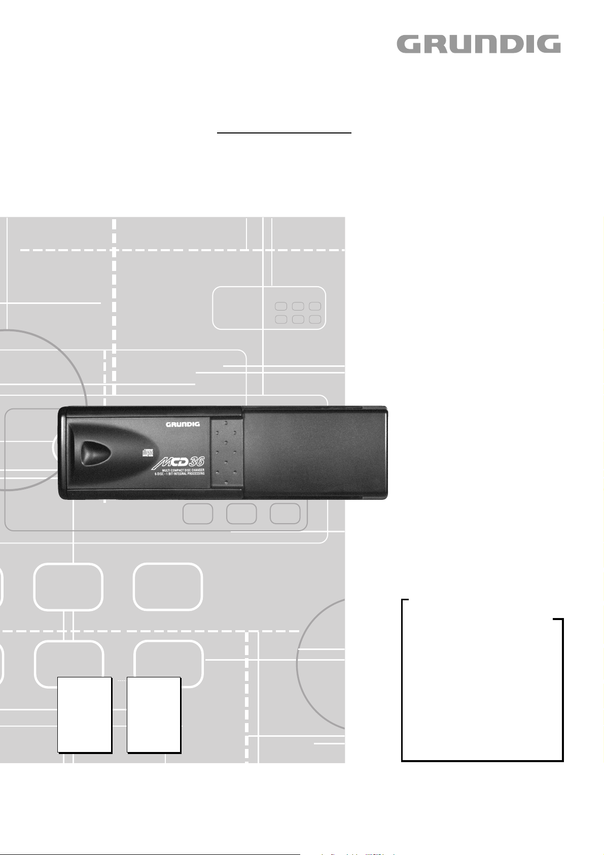
MCD 36
(G.HF 2800)
MCD 40
(G.HF 2900)
Zusätzlich erforderliche Unterlagen für den Komplettservice
Additionally required Service Documents for the Complete Service
Service
Manual
MCD 36
MCD 40
Materialnr./Part No.
72010 748 3000
Materialnummer/Part Number 72010 748 3100
Änderungen vorbehalten/Subject to alteration • Printed in Germany
E-BS 36 0400 • 9033
http://www.grundig.com
Service
Manual
Sicherheit
Safety
Materialnr./Part No.
72010 800 0000
Grundig Service
Hotline Deutschland...
Technik:
TV
TV
SAT
VCR/LiveCam
HiFi/Audio
Car Audio
Telekommunikation
Planatron
Ersatzteil-Verkauf: ...Mo.-Fr. 8.00-19.00 Uhr
(8.00-22.00 Uhr)
...Mo.-Fr. 8.00-18.00 Uhr
0180/52318-41
0180/52318-49
0180/52318-48
0180/52318-42
0180/52318-43
0180/52318-44
Fax:
Telefon:
Fax:
0180/52318-45
0180/52318-51
0180/52318-99
0180/52318-40
0180/52318-50
Page 2

Allgemeiner Teil / General Section MCD 36 / MCD 40
Es gelten die Vorschriften und Sicherheitshinweise
gemäß dem Service Manual "Sicherheit", Materialnummer 72010 800 0000, sowie zusätzlich die eventuell abweichenden, landesspezifischen Vorschriften!
Dieses Service Manual gilt für die Geräte MCD 36 und MCD 40 ab
folgenden Seriennummern:
MCD 36: 01 00995 0 521 284501
MCD 40: 01 00996 0 521 119801
Für Geräte mit niedrigeren Seriennummern verwenden Sie bitte
das Service Manual mit der Materialnummer 72010 748 3000.
D
Inhaltsverzeichnis
Seite
Allgemeiner Teil ............................ 1 - 2 … 1 - 6
Technische Daten ..................................................................... 1 - 2
Ausbauhinweise ........................................................................ 1 - 3
Steuerungsablauf der Mechanik ............................................... 1 - 6
Schaltpläne und
Druckplatten-Abbildungen ......... 2 - 1 … 2 - 16
Blockschaltplan ......................................................................... 2 - 1
Verdrahtungsplan ...................................................................... 2 - 2
Schaltplan ................................................................................. 2 - 3
Pick-Up-Einheit ......................................................................... 2 - 7
Spannungen .............................................................................. 2 - 8
Druckplatten-Abbildungen ......................................................... 2 - 9
IC-Innen-Beschaltungen ......................................................... 2 - 11
The regulations and safety instructions shall be valid
as provided by the "Safety" Service Manual, part
number 72010 800 0000, as well as the respective
national deviations.
This Service Manual is valid for MCD 36 and MCD 40 from the
following serial numbers on:
MCD 36: 01 00995 0 521 284501
MCD 40: 01 00996 0 521 119801
For sets with lower serial numbers please use the Service Manual
with the part number 72010 748 3000.
GB
Table of Contents
Page
General Section ............................. 1 - 2 … 1 - 6
Technical Data .......................................................................... 1 - 2
Disassembly Instructions .......................................................... 1 - 3
Flowchart of Control Operation of Mechanism .......................... 1 - 6
Circuit Diagrams and
Layout of PCBs ........................... 2 - 1 … 2 - 16
Block Diagram ........................................................................... 2 - 1
Wiring Diagram ......................................................................... 2 - 2
Circuit Diagram ......................................................................... 2 - 3
Pick Up Unit .............................................................................. 2 - 7
Voltages .................................................................................... 2 - 8
Layout of PCBs ......................................................................... 2 - 9
IC Block Diagrams .................................................................. 2 - 11
Explosionszeichnungen
und Ersatzteilliste ......................... 3 - 1 … 3 - 6
Allgemeiner Teil
Messgeräte / Messmittel
Beachten Sie bitte das GRUNDIG Messtechnik-Programm, das Sie
unter folgender Adresse erhalten:
GRUNDIG Instruments Test- und Messsysteme GmbH
Würzburger Str. 150, D-90766 Fürth/Bay
Tel. 0911/703-4118, Fax 0911/703-4130
eMail: instruments@grundig.de; Internet: http://www.grundig.instruments.de
Technische Daten
D/A-Wandler ............................................................................. 1 Bit
Oversampling-Rate ................................................................. 8 fach
Frequenzbereich ........................................................ 20Hz…20kHz
Geräuschspannungsabstand ................................................... 95dB
Gleichlaufschwankung .......................................... unter Meßgrenze
Klirrfaktor (1kHz) .................................................................. 0,008%
Nenn-Ausgangspegel ............................................................. 0,68V
Nenn-Ausgangsimpedanz .......................................................... 1kΩ
Stromaufnahme .................................................................... 400mA
Betriebstemperatur .................................................. -10˚C … +50˚C
Gewicht ca. ................................................................................. 2kg
Abmessungen
(MCD 36) .......................................................... 25 x 6,4 x 16cm
(MCD 40) .......................................................... 25 x 8,1 x 16cm
Exploded Views and
Spare Parts List ............................. 3 - 1 … 3 - 6
General Section
Test Equipment / Aids
Please note the Grundig Catalog "Test and Measuring Equipment"
obtainable from:
Technical Data
D/A Converter ............................................................................ 1Bit
Oversampling Rate ............................................................... 8 times
Frequency Range ...................................................... 20Hz…20kHz
Signal/Noise Ratio ................................................................... 95dB
Wow and Flutter ................................................... immeasurably low
Distortion Factor (1kHz) ....................................................... 0.008%
Nominal Output Level ............................................................. 0.68V
Nominal Output Impedance ....................................................... 1kΩ
Current Consumption ............................................................ 400mA
Operating Temperature ............................................ -10˚C … +50˚C
Weigth approx. ............................................................................ 2kg
Dimensions
(MCD 36) ........................................................... 25 x 6.4 x 16cm
(MCD 40) ........................................................... 25 x 8.1 x 16cm
1 - 2 GRUNDIG Service
Page 3
MCD 36 / MCD 40 Allgemeiner Teil / General Section
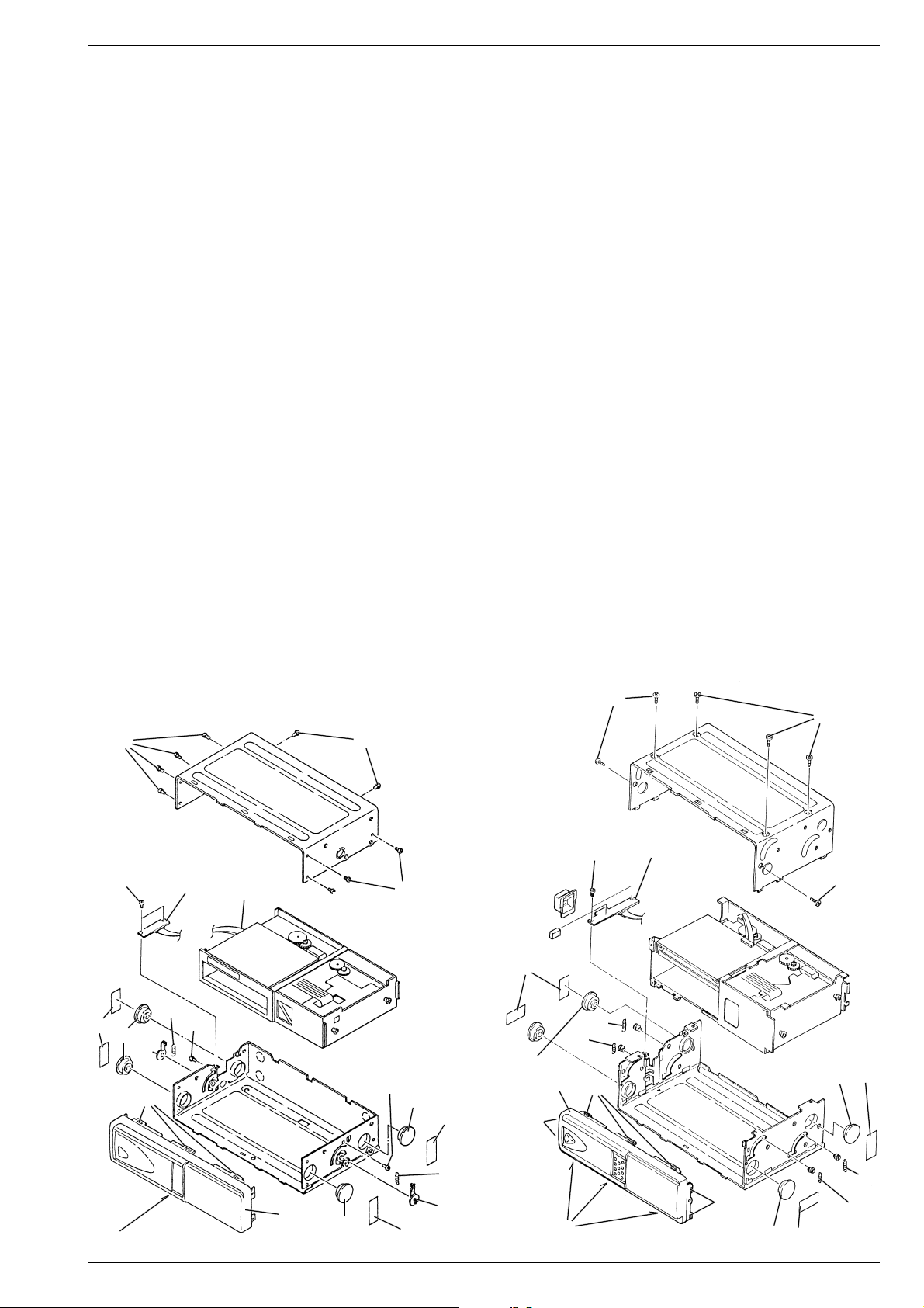
Ausbauhinweise
1a. Zerlegen des Gehäuses (MCD 36)
Gehäuseoberteil abnehmen (Fig. 1a)
- Die 9 Schrauben A herausschrauben.
- Die 4 Rastnasen 1 ausrasten und die Frontblende 2 nach vorne
abziehen.
- Gehäuseoberteil an der rechten Seite ausrasten, nach links hochklappen und abnehmen.
Gehäuseunterteil abnehmen (Fig. 1a)
- Die 2 Schrauben B herausschrauben und Anschluss-Platte C
abnehmen.
- Die 4 Klebstreifen 8 abziehen und die 4 Dämpfer 7 nach aussen
herausziehen.
- Die Federn 5 und 6 aushängen.
- Gehäuseunterteil abnehmen.
Hebel 4 ausbauen (Fig. 1a)
- Die 2 Schrauben E herausschrauben.
- Die Hebel 4 bis zur Aussparung drehen und nach aussen herausnehmen.
1b. Zerlegen des Gehäuses (MCD 40)
Gehäuseoberteil abnehmen (Fig. 1b)
- Die 6 Schrauben A herausschrauben.
- Die 10 Rastnasen 1 ausrasten und die Frontblende 2 nach vorne
abziehen.
- Gehäuseoberteil an der rechten Seite ausrasten, nach links hochklappen und abnehmen.
Gehäuseunterteil abnehmen (Fig. 1b)
- Die 2 Schrauben B herausschrauben und Anschluss-Platte C
abnehmen.
- Die 4 Klebstreifen 8 abziehen und die 4 Dämpfer 7 nach aussen
herausziehen.
- Die Federn 5 und 6 aushängen.
- Gehäuseunterteil abnehmen.
Disassembly Instructions
1a. Disassembling of the Cabinet (MCD 36)
Removing the upper part of the cabinet (Fig. 1a)
- Undo 9 screws A.
- Disengage 4 catches 1 and pull the front panel 2 towards the
front.
- Detach the top of the cabinet on the right side and raise it towards
the left to remove it.
Removing the bottom part of the cabinet (Fig. 1a)
- Undo 2 screws B and remove the Connection Board C.
- Remove the 4 pieces of adhesive tape 8 and pull out the 4
dampers 7.
- Unhook the springs 5 and 6.
- Remove the bottom part of the cabinet.
Removing the levers 4 (Fig. 1a)
- Undo 2 screws E.
- Turn the levers 4 to the outcut and take them out.
1b. Disassembling of the Cabinet (MCD 40)
Removing the upper part of the cabinet (Fig. 1b)
- Undo 6 screws A.
- Disengage 10 catches 1 and pull the front panel 2 towards the
front.
- Detach the top of the cabinet on the right side and raise it towards
the left to remove it.
Removing the bottom part of the cabinet (Fig. 1b)
- Undo 2 screws B and remove the Connection Board C.
- Remove the 4 pieces of adhesive tape 8 and pull out the 4
dampers 7.
- Unhook the springs 5 and 6.
- Remove the bottom part of the cabinet.
MCD 36
A
B
8
7
4
1
5
C
E
D
A
E
A
7
8
MCD 40
8
7
1
2
5
B
6
1
A
C
A
A
7
8
6
1
7
8
8
4
1
2
1
GRUNDIG Service 1 - 3
Fig. 1a Fig. 1b
7
6
5
Page 4
Allgemeiner Teil / General Section MCD 36 / MCD 40
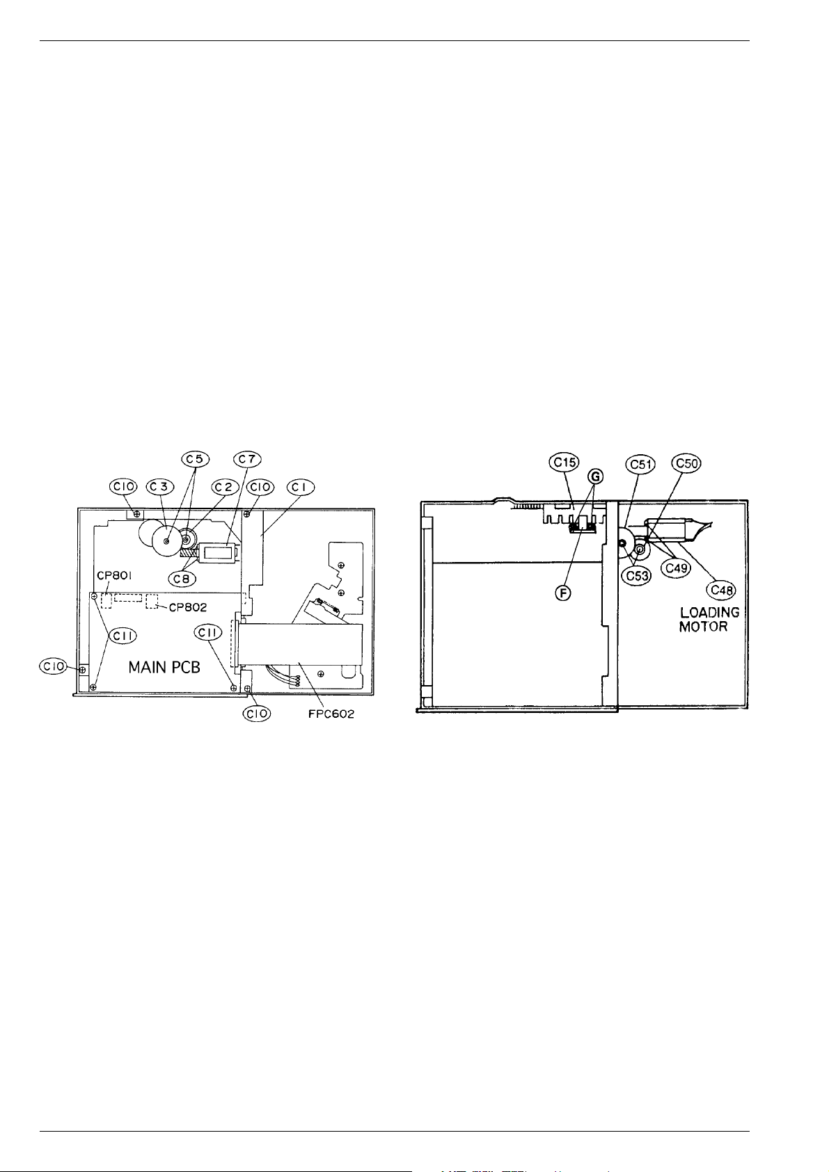
2. Hauptplatte ”MAIN PCB” ausbauen (Fig. 2)
- Gehäuseoberteil abnehmen (Pkt. 1).
- 3 Schrauben C11 herausschrauben.
- Steckverbindungen lösen.
- Leiterplatte herausnehmen.
3. Ausbau des Lift-Motors C7 (Fig. 2)
- Hauptplatte ”MAIN PCB” ausbauen (Pkt 2).
- Kunststoffscheiben C5 abziehen.
- Zahnräder C2 und C3 abnehmen.
- 2 Schrauben C8 herausschrauben.
- Lift-Motor C7 ablöten und herausnehmen.
4. Ausbau des Loading-Motors C48
- Hauptplatte ”MAIN PCB” ausbauen (Pkt 2).
- 4 Schrauben C10 herausschrauben und Magazinschacht-Oberteil
C1 herausnehmen (Fig. 2).
- Kunststoffscheiben C53 abziehen (Fig. 3).
- Zahnräder C50 und C51 herausnehmen (Fig. 3).
- 2 Schrauben C49 herausschrauben (Fig. 3).
- Loading-Motor C48 ablöten und herausnehmen (Fig. 3).
5. Ausbau des Optokopplers J
- Hauptplatte ”MAIN PCB” ausbauen (Pkt 2).
- 4 Schrauben C10 herausschrauben und Magazinschacht-Oberteil
C1 herausnehmen (Fig. 2).
- 2 Schrauben I herausschrauben (Fig. 3).
- Optokoppler J ablöten und herausnehmen.
2. Removing the Main Board (Fig. 2)
- Remove the upper part of the cabinet (para 1).
- Undo 3 screws C11.
- Unplug all connectors.
- Take out the PCB.
3. Removing the Lift Motor C7
- Remove the Main Board (para 2).
- Loosen and remove the plastic washers C5.
- Pull off the gear wheels C2 and C3.
- Undo 2 screws C8.
- Unsolder the Lift Motor C7 and take it out.
4. Removing the Loading Motor C48
- Remove the Main Board (para 2).
- Undo 4 screws C10 and remove the cover plate of the CD magazine
compartment C1 (Fig. 2).
- Loosen and remove the plastic washers C53 (Fig. 3).
- Pull off the gear wheels C50 and C51 (Fig. 3).
- Undo 2 screws C49 (Fig. 3).
- Unsolder the Lift Motor C48 and take it out (Fig. 3).
5. Removing the Opto Coupler J
- Remove the Main Board (para 2).
- Undo 4 screws C10 and remove the cover plate of the CD magazine
compartment C1 (Fig. 2).
- Undo 2 screws I (Fig. 3).
- Unsolder the Opto Coupler J and take it out.
Fig. 2 Fig. 3
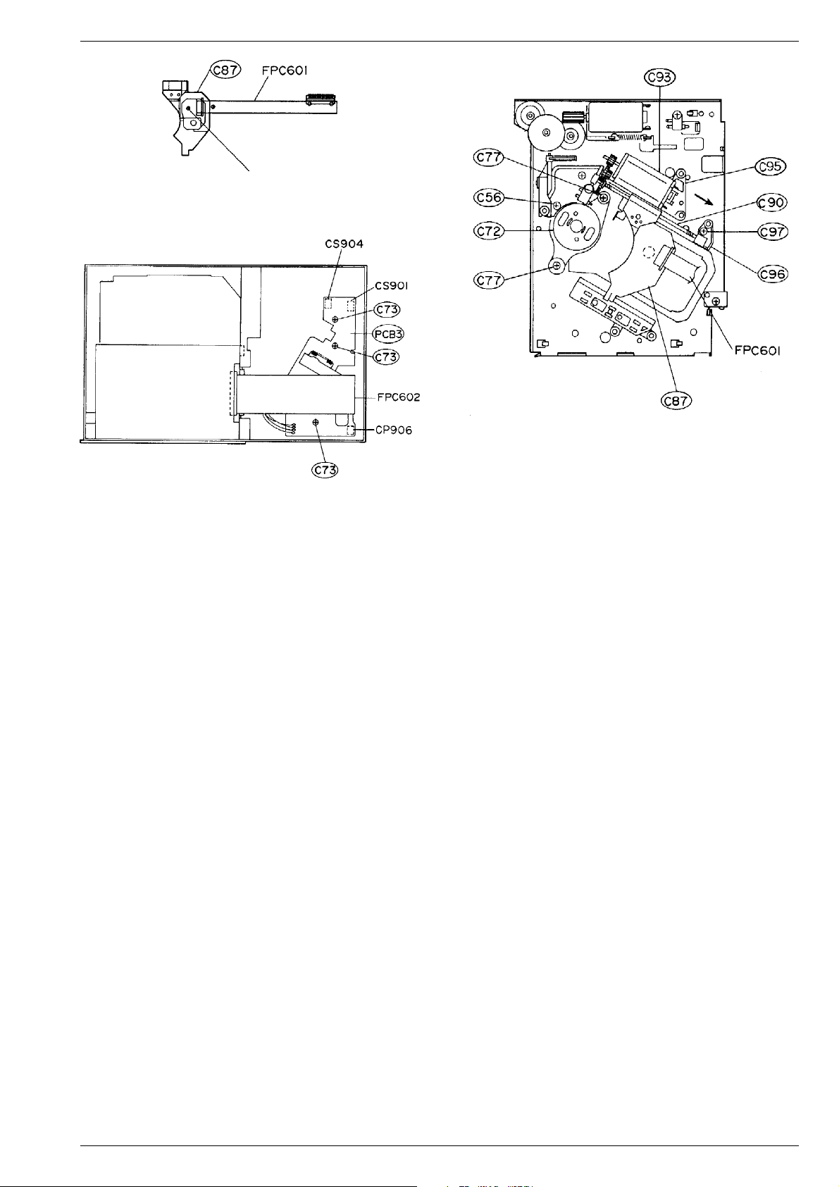
6. CD-Leiterplatte PCB3 und Pick-Up-Einheit C87 ausbauen
-
Wichtig:
Vor dem Ausbau der Pick-Up-Einheit müssen die bei-
den Lötstellen auf der Pick-Up-Einheit kurzgeschlossen werden! (Fig. 4)
- Gehäuse zerlegen (Pkt. 1).
- Steckverbindungen FPC602, CS901, CP904 und CP906 lösen
(Fig. 5).
- 3 Schrauben C73 herausschrauben (Fig. 5).
- Schraube C97 und Schraube C96 herauschrauben (Fig. 6).
- Achse C90 herausziehen (Fig. 6).
- Pick-Up-Einheit herausnehmen.
- Steckverbindung FPC601 lösen (Fig. 4) und CD-Leiterplatte PCB3
herausnehmen.
7. Disc-Motor C72 ausbauen (Fig. 6)
- Pick-Up-Einheit ausbauen (Pkt. 6).
- 2 Schrauben C77 herausschrauben und Disc-Motor herausneh-
men.
6. Removing the CD Board PCB3 and the Pick Up Unit C87
-
Important:
Before removing the Pick Up Unit the two solder tags
on the Pick Up Unit must be connected (Fig. 4).
- Disassemble the cabinet (para 1).
- Unplug the connectors FPC602, CS901, CP904 and CP906 (Fig. 5).
- Undo 3 screws C73 (Fig. 5).
- Undo screws C97 and C96 (Fig. 6).
- Pull out the shaft C90.
- Take out the Pick Up Unit.
- Unplug the connector FPC601 (Fig. 4) and take out the CD Board
PCB3.
7. Removing the Disc Motor C72 (Fig. 6)
- Remove the Pick Up Unit (para 6).
- Undo 2 screws C77 and remove the Disc Motor.
1 - 4 GRUNDIG Service
Page 5
MCD 36 / MCD 40 Allgemeiner Teil / General Section
kurzschliessen
short circuit
Fig. 4
Fig. 6
Fig. 5
GRUNDIG Service 1 - 5
Page 6
Allgemeiner Teil / General Section MCD 36 / MCD 40
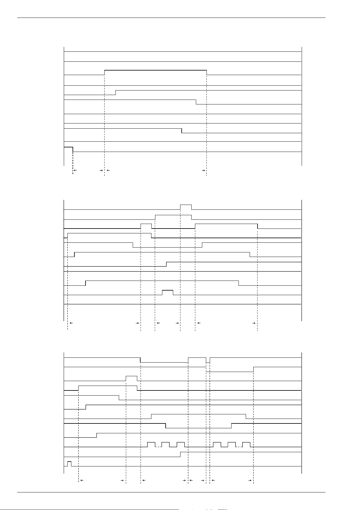
Steuerungsablauf der Mechanik Flowchart of Control Operation of Mechanism
MAGAZIN IN
H
ELV (LIFT) +
ELV (LIFT) -
LOAD +
LOAD -
LOADOUT
CLAMP
UPLIMIT
LOWLIMIT
DISC ON
DISC COUNT
MAG.SW
L
H
L
H
L
H
L
H
L
H
L
H
L
H
L
H
L
H
L
H
L
DISC CHANGE (DISC 1 / 2)
ELV (LIFT) +
ELV (LIFT) -
LOAD +
LOAD -
LOADOUT
CLAMP
UPLIMIT
LOWLIMIT
DISC ON
DISC COUNT
MAG.SW
H
L
H
L
H
L
H
L
H
L
H
L
H
L
H
L
H
L
H
L
H
L
0.6sec
1.5sec
(DISC UNLOADING)
1.5sec
(DISC LOADING)
0.2sec
(ELV DOWN)
1.5sec
(DISC LOADING)
MAG EJECT(DISC 1 PLAY)
ELV (LIFT) +
ELV (LIFT) -
LOAD +
LOAD -
LOADOUT
CLAMP
UPLIMIT
LOWLIMIT
DISC ON
DISC COUNT
MAG.SW
EJECT
H
L
H
L
H
L
H
L
H
L
H
L
H
L
H
L
H
L
H
L
H
L
H
L
1.5sec
(DISC UNLOADING)
1101110 1
2.5sec
(ELV DOWN)
2sec
3.0sec
(ELV UP)
1 - 6 GRUNDIG Service
Page 7

MCD 36 / MCD 40 Schaltpläne und Druckplattenabbildungen / Circuit Diagrams and Layout of PCBs MCD 36 / MCD 40 Schaltpläne und Druckplattenabbildungen / Circuit Diagrams and Layout of PCBs
LD
OPTICAL
PICK UP
Q601
SWITCH
DISC MOTOR
FEED MOTOR
IC651 DRIVER
IC650
SERVO
CONTROLLER
IC601
DIGITAL SIGNAL
PROCESSOR
&
DAC
VRMDGND
Vcc
VREF
COM
PD1
PD2EFF+F–T+T–
CLUMP
DISC
ON
D101
Q901
D910
DISC
COUNT
BUFFER
LOADING
MOTOR
IC950
MOTOR
DRIVER
IC806
MOTOR
DRIVER
ELEVATOR
MOTOR
IC807
LOAD
LOW
UP
INSIDE
MAG.IN
M
M
M
M
F+
F–
F+
T–
SP+
SP–
SL+
SL–
T IN
LDS
LDD
CLK
4.2M
X OUT
X IN
TD
FD
SPD
SLD
SL+
SL–
DRF
CE
DAT
CL
SQ OUT
WRQ
LOAD+
LOAD–
ELV+
FEM+
FEM–
DRF
RWC
COIN
CQCK
SQ OUT
WRQ
DS
RESET
ELV–
DS RESET
F IN
SPD
IN
SLD
IN
DISC ON
CLUMP
DISC COUNT
MAG. SW
LOWUPINSIDE
LOAD
FIN2
SLI
RCHO
EFMO
X601
SWITCH
Q803,804,950
Q900
Q805
REGULATOR
DIN
REGULATOR
+12V
+8V
D5V
L.P.F.
IC701
L.P.F.
IC701
Q801,802
IC801
␣ -COM
IC803
IC802
IC804
RESET
BATTERY
SWITCH
DETECT
U+5V
EFMI
CLV+
CLV–
V/P
HFL
TOFF
TGU
TP+
/CQCK
COIN
RWC
TP–
LCHO
RF SW
CLV+
CLV–
SLOF
HFL
TOFF
TGL
DATA 1
DATA 0
BATT
Acc
CD+B
RESET
POWER
TP+
TP–
FIN1EF
2
4
1
6
7
3
5
8
S
PICKUP
FPC FPC602 FPC602
MAIN
12A/L
VC
VCC
11
10
9
7
6
5
4
3
2
1
13
14
15
16
8NC
11
10
9
8
7
6
5
4
3
2
1
12
13
14
15
14
15
14
15
1
2
3
4
5
6
7
8
9
10
11
12
13
1
2
3
4
5
6
7
8
9
10
11
12
13
F-
F+
NL
F
VC
VCCLDGNDVRMDEPD1
PD2T+T-
29
30
16
17
18
19
20
21
22
23
24
25
26
27
28
DOWN
GND
LM+
LM-
CLAMP
LOAD0
DION
LED
SL-
SL+
SP-
SP+
GND
INSIDE
UP
29
30
16
17
18
19
1
CS901
DISC LED
D901
LOAD MOTOR
CLAMP SW
FEED MOTOR
DISC MOTOR
INSIDE SW
LOAD SW
Q901
DISK ON
2
3
4
4
3
4
3
2
1
2
1
2
1
3
2
1
3
2
1
2
1
4
3
2
1
20
21
22
23
24
25
26
27
28
2
1
CS501
CP501 CP801
MAG SW
ELV MOTOR
DISC CHG
D910 LED
CP802
B.UP
3
4
5
213
213
4
5
6
7
2
1
CS505
3
4
5
6
8
7
8
9
2
1
2
1
EM+
EM-
DISC.C
GND
LED
MAG.SW
GND
3
4
5
6
7
8
9
ACC
B.UP.1
B.UP
CD+B
BUS
GND
R-CH
SGND
L-CH
CONNECT
PHOTO
CS602 CS602
SENSOR
SENSOR
SWITCH
CP906 CS906
UP SW
LOW SW
Q901 : PT4850F
D901 : SLR-989A
D910 : GP1S51V
CD
FPC603
S
Schaltpläne und Druckplatten-Abbildungen / Circuit Diagrams and Layout of PCBs
Blockschaltplan / Block Diagram
Verdrahtungsplan / Wiring Diagram
GRUNDIG Service GRUNDIG Service
Page 8

Schaltpläne und Druckplattenabbildungen / Circuit Diagrams and Layout of PCBs MCD 36 / MCD 40
A: 2ms
5
: 50mV9: 500mV
VC™
MODE: Forward Search
VC™
5
9
Schaltpläne und Druckplattenabbildungen / Circuit Diagrams and Layout of PCBs MCD 36 / MCD 40
Schaltplan / Circuit Diagram
MODE: Play
VC™
A: 500ns
1
: 500mV
LED DRIVER
MODE: Play
1
VC™
VC™
A: 1ms
5
: 50mV6: 50mV
5
6
MODE: Play
VC™
VC™
A: 1ms
2
: 50mV3: 50mV
2
3
MODE: Play
VC™
VC™
A: 200∝s
7: 50mV 8: 50mV
7
8
MODE: Focus Search
VC™
A: 100ms
4: 50mV
4
5
VC
2
34
6
SERVO CONTROL
7
8
1
9
DEFECT
COMPARATOR
SWITCH
DEFECT
COMPARATOR
DSP & D/A
MUTE
REGULATOR
MUTE
SERVO DRIVER
SWITCH
MUTE
GRUNDIG Service GRUNDIG Service
2 - 42 - 3
Page 9

MCD 36 / MCD 40 Schaltpläne und Druckplattenabbildungen / Circuit Diagrams and Layout of PCBs MCD 36 / MCD 40 Schaltpläne und Druckplattenabbildungen / Circuit Diagrams and Layout of PCBs
REGULATOR
EJECT
MODE
SWITCH
SWITCH
SWITCH
INVERTER
MOTOR
DRIVER
LC66566B-4K60
CONTROL
MICRO COMPUTER
SWITCH
DETECTOR
DETECTOR
SWITCH
REGULATOR
REGULATOR
REGULATOR
MOTOR
DRIVER
GRUNDIG Service GRUNDIG Service2 - 5 2 - 6
Page 10

Schaltpläne und Druckplattenabbildungen / Circuit Diagrams and Layout of PCBs MCD 36 / MCD 40
IC601
IC
IC
PIN
12345678910111213141516
0 0 1.5 0 1.6 5 0.3 0 0/5
1.4/3.3
0 0/5 0 0 0 0/5
17 18 19 20 21 22 23 24 25 26 27 28 29 30 31 32
05000/50/55000000 0
33 34 35 36 37 38 39 40 41 42 43
44
48
0 HiZ 0 5 2.2 0 0 2.2 5 0 5 -1/5 0/5
49 50 51 52 53 54 55 56 57 58 59 60 61 62 63 64
0/5 0/5 0 0/5 0/5 0/5 0/5 4.8 0/5 4.8 0
-1.5/6.5 -0.6/5.4
000
0
45
0/5460
0/5
IC806
PIN
12345678910
0 11.5 HiZ HiZ 0 HiZ 11.5 HiZ 7.8 0
IC
IC950
PIN
12345678910
0 11.5 HiZ HiZ 0 HiZ 11.5 HiZ 7.8 0
IC
IC681
PIN
12345678
0.1 3 2.2 0 2.2 2.2 0.1 5
IC
IC701
PIN
12345678
2.5 2.5 2.5 0 2.5 2.5 2.5 7.5
47
0/5
PIN
B
3.8
0
0.1
8.2
0
0
0
0.6
0
0.9
12.6
4.3
8.4
0.8
Q601
Q681
Q682
Q700
Q701
Q702
Q703
Q801
Q802
Q803
Q804
Q805
Q900
Q950
C
2
2.2
2.2
11.5
0
0
0
0
4.8
11.8
11.5
HiZ
11.5
0.9
E
4.5
0
0
7.5
0
0
0
0
4.8
0
13.2
4.8
7.8
0
IC650
IC
PIN
12345678910111213141516
2.5 2.5 2.5 2.5 2.5 2.5 2.5 2.5 2.5 2.5 2.5 2.5 2.5 2.5 2.5 2.3
17 18 19 20 21 22 23 24 25 26 27 28 29 30 31 32
2.5 2.6 2.5 2.5 2.5 0 2.4 2.4 2.4 2.5 2.9 2.5 2.6 0
33 34 35 36 37 38 39 40 41 42 43
44
48
0500/50000/5
1.4/3.5
2.4 2.7
2.5
HiZ
49 50 51 52 53 54 55 56 57 58 59 60 61 62 63 64
0
-0.6/5.4
0/5 4.8 0/5 4.9 HiZ 5 2.5 2.5 2.6 2.7 2.2 3.8 0.2 5
2.3
45
0
46
2.5
2.3
47
2.5
IC801
IC
PIN
12345678910111213141516
4.800000000050.14.80
0/4.5
HiZ
17 18 19 20 21 22 23 24 25 26 27 28 29 30 31 32
0000
0/4.5
0 0 1.9
1.2/3.6
4.7 4.8 0 0 0
33 34 35 36 37 38 39 40 41 42 43
44
48
00000001.71.93.73.7
4.8
0
49 50 51 52 53 54 55 56 57 58 59 60 61 62 63 64
5 4.8 0 4.8 4.8 4.8 0 4.8 0/5 4.8 0/5 0/5 0 0/5 0 4.4
3.6
45
0
46
0
0
47
4.9
IC651
IC
PIN
12345678910111213141516
7.8 2.5 2.5 2.5 2.5 2.8 0 0 7.8 7.8 3.4 4.1 3.5 3.9 3.7 3.7
17 18 19 20 21 22 23 24 25 26 27 28
3.3 4 7.8 HiZ 0 2.5 2.5 0.8 2.3 2.5 2.6 2.5
IC
IC
IC
IC
IC804
PIN
12345
HiZ 0 0 4.7 4.7
IC
IC807
PIN
12345
HiZ 4.6 0 0 5
IC802
PIN
123
13.2 5.4 0.4
IC803
PIN
123
4.8 8.2 0
IC805
PIN
123
11.5 5 0
Schaltpläne und Druckplattenabbildungen / Circuit Diagrams and Layout of PCBs MCD 36 / MCD 40
Schaltplan Pick-Up-Einheit / Circuit Diagram Pick Up Unit
Spannungen / Voltages (gemessen bei UB = 14V bei PLAY / measured with UB = 14V at PLAY)
2 - 7 2 - 8
GRUNDIG Service GRUNDIG Service
Page 11

MCD 36 / MCD 40 Schaltpläne und Druckplattenabbildungen / Circuit Diagrams and Layout of PCBs MCD 36 / MCD 40 Schaltpläne und Druckplattenabbildungen / Circuit Diagrams and Layout of PCBs
Druckplatten-Abbildungen / Layout of PCBs
GRUNDIG Service GRUNDIG Service2 - 9 2 - 10
Page 12

Schaltpläne und Druckplattenabbildungen / Circuit Diagrams and Layout of PCBs MCD 36 / MCD 40
PIN
1
2
3
4
5
6
7
8
9
10
11
12
13
14
15
16
17
18
19
20
21
22
23
24
25
26
27
28
29
30
31
32
33
34
35
36
37
38
39
40
41
42
43
44
45
46
47
48
49
50
51
52
53
54
DESCRIPTION
Pickup photo-diode connecting pin. Forms RF signal by addition to FIN1 pin,and FE signal by
subtraction.
Pickup photo-diode connecting pin.
Pickup photo-diode connecting pin. Forms TE signal by subtraction from F pin.
Pickup photo-diode connecting pin.
Pin for inputting DC constituent of TE signal.
Pin for connecting gain setting resistence of TE signal to TE pin.
TE signal output pin.
TES(TRACK ERROR SENCE) comparator input pin. Band pass TE signal, and input.
Input pin for shock detection.
Constant setting pin at the time of tracking gain.
Pin for connecting high pass elimination condensor of servo.
Pin for constituting tracking phase compensation constant between TD and VR pin.
Pin for setting tracking phase compensation.
Pin for setting tracking jump signal (kick pulse) amplitude.
Tracking control signal output pin.
Focusing control signal output pin.
Pin for constituting focussing phase compenstion constant between FD and FA pin.
Pin for constituting focussing phase compensation constant between FA- and FE- pin.
Pin for constituting focussing phase compensation constant between FA and FE pin.
FE signal output pin.
Pin for connecting FE signal gain setting resistance to TE pin.
GND for analog signal.
Signal end output of CV+ and CV- pin input signal
.
Connecting pin for spindle phase compensation constant together with SPD pin.
Spindle control signal output pin.
Connecting pin for sled phase compensation constant.
Sled control signal output pin.
Input pin for sled delivery signal from micro computer.
Input pin for sled delivery signal from micro computer.
Input pin for tracking jump signal from DSP.
Input pin for tracking jump signal from DSP.
Input pin for tracking gain control signal from DSP.Gain low in case of TGL="H".
Input pin for tracking off control signal from DSP.Off in case of TOFF="H".
Output pin of TES signal to DSP.
(HIGH FREQENCY LEVEL) is used to judge whether main beam is located
above pit or above mirror.
Sled servo off control input pin.
Input pin for CLV error signal from DSP.
Input pin for CLV error signal from DSP.
RF output pin.
Pin for setting RF gain and EFM signal 3T compensation constant together with RFSM pin.
(SLICE LEVEL CONTROL) is output pin for controlling data slice level by RF waveshape DSP.
Input pin for controlling data slice level by DSP.
GND pin digital system.
For Focs Smoosing capacita output pin.
Tracking Balance control pin.
NO CONNECT.
Output pin for detecting disc defect.
Standard clock input pin. DSP 4.23MHz is input.
Micro computer command clock input pin.
Micro computer command data input pin.
(DEFECT RF) RF level detecting output.
Micro computer command chip enable input pin.
Spindle amplifier input.
Connecting pin for gain setting resistance at the time of spindle 12cm mode.
PORT NAME
FIN2
FIN1
E
F
TB
TE-
TE
TESI
SCI
TH
FIN1
TA
TD-
TD
JP
TO
FD
FD-
FA
FA-
FE
FE-
AGND
SP
SPI
SPG
SP-
SPD
SLEQ
SLD
SL-
SL+
JP-
JO+
TGL
TOFF
TES
HFL
SLOF
CV-
CV+
RFSM
RFS-
SLC
SLI
DGND
FSC
TBC
NC
DEF
CLK
CL
DAT
CE
DRF
55
56
57
58
59
60
61
62
63
64
Focs serch select pin.
VCC pin for servo system and digital system.
Connection pin for standard voltage capacitor.
Standard voltage output pin.
Pin for setting constant at the time of detecting disc defect.
Pin for connecting condensor for RF signal peak hold.
Pin for connecting condensor for RF signal bottom hold.
APC circuit output pin.
APC circuit input pin.
RF system VCC pin.
FSS
VCC2
REF1
VR
LF2
PH1
BH1
LDD
LDS
VCC1
Schaltpläne und Druckplattenabbildungen / Circuit Diagrams and Layout of PCBs MCD 36 / MCD 40
IC-Innen-Beschaltungen / IC Block Diagrams
NJM2100M
–INPUT
+INPUT
V
IN
GND
VDD
VSS
2,6
3,5
S-81250HG-RD
V
REF
1
S-8054HN
2
7
OUT32
OUT1
FIN2
FIN1
TB
TE–
TE
TESI
SCH
TH
TA
TD–
TD
JP
TO
FD
8
V+
1,7
OUTPUT
4
V–
VCC1
LDS
LDD
BHI
PHI
64 63 62 61 60 59 58 57 56 55 54 53 - 50 49
APC
RF DET
1
BAL
VCA
VCA
2
I/V
E
3
F
4
5
6
TE
7
8
9
T.SERVO &
T.LOGIC
10
11
12
13
F.SERVO &
F.LOGIC
14
15
16
17 18 19 20 2122 23 24 25 26 27 28 29 30 31 32
FA
FA–FEFE–
FD–
LF2VRREF1
VCC2NCDRFCEDATCLCLK
REF
LA9240MS
∝-COM
INTERFACE
SPINDLE
SERVO
SP
SPI
AGND
SP–
SPG
SLC
RF
AMP
SLED SERVO
SLD
SPD
SLEQ
LA 9240 MS
DEF
48
NC
47
NC
46
NC
45
DGND
44
SLI
43
SLC
42
RFS–
41
RFSM
40
CV+
39
CV–
38
SLOF
37
HFL
36
TES
35
TOFF
34
TGL
33
JP+
JP–
SL–
SL+
GRUNDIG Service GRUNDIG Service
2 - 122 - 11
Page 13

MCD 36 / MCD 40 Schaltpläne und Druckplattenabbildungen / Circuit Diagrams and Layout of PCBs MCD 36 / MCD 40 Schaltpläne und Druckplattenabbildungen / Circuit Diagrams and Layout of PCBs
1
2
3
4
5
6
7
8
9
10
11
12
13
14
15
16
17
18
19
20
21
22
23
24
25
26
27
28
29
30
31
32
33
34
35
36
37
38
39
40
41
42
43
44
45
46
47
48
49
50
51
52
53
54
55
56
57
58
59
60
61
62
63
64
Initial setting input terminal for changer 1 or 2 switching
Play mode output H:play mode
Load/spindle motor switching signal output
No connection
No connection
No connection
No connection
No connection
Disc clamp finish SW input
Elevator upper limit SW input
Elevator lower limit SW input
Magazine detection SW input
CD mode signal output
No connection
Status data output
No connection
No connection
No connection
No connection
No connection
Command data input
Connection to ground
Ground
Ceramic oscillator connection terminal for system clock
Ceramic oscillator connection terminal for system clock
Reset signal input
Battery LOW detection input
No connection
No connection
Main & servo system power supply ON/OFF output
No connection
No connection
No connection
Pickup moving-inside signal output
Pickup moving-outside signal output
Output to move a tray in the direction out of magazine with loading motor
Output to move a tray in the direction into magazine with loading motor
No connection
No connection
Reference voltage for TH1
Reference voltage for TH2
Temperature sensor ON signal input
Temperature sensor OFF signal input
Acc ON/OFF detection signal input
Disc detection photo transistor signal input
Magazine eject key signal input
Focus OK signal input
No connection
Elevator position detection pulse input
Initial setting input terminal for 6 discs changer or 10 discs changer
Mute signal output
Reset signal for DSP(LC78622E)
Magazine tray detection SW input
Inner circle limit detection SW input
No connection
Power supply (+5V)
Interface with DSP(LC78622E)
Interface with DSP(LC78622E)
Interface with DSP(LC78622E)
Interface with DSP(LC78622E)
Elevator moving-down signal output
Interface with DSP(LC78622E)
Elevator moving-up signal output
Stand by position cancellation signal input
MODE
PLAY
LD/SP
NC
NC
NC
NC
NC
CLAMPSW
UPLIMIT
LOWLIMIT
MAGZSW
CD+B
NC
DATAOUT
NC
NC
NC
NC
NC
DATAIN
TEST
VSS
OSC1
OSC2
RESET
BATT
NC
NC
POWER
NC
NC
NC
FEM-
FEM+
LOAD+
LOAD-
NC
NC
VREF0
VREF1
TH1
TH2
ACC
DISCON
EJECT
DRF
NC
DISCCOUNT
6/10CD
MUTE
DSPRST
LOADOUT
INSIDESW
NC
VDD
SQOUT
COIN
CQCK
WRQ
ELV-
RWC
ELV+
STBY
I
O
O
O
O
O
O
O
I
I
I
I
O
O
O
O
O
O
O
O
I
I
I
I
O
O
O
O
O
O
O
O
O
O
O
O
I
I
I
I
I
I
I
I
O
I
I
O
O
I
I
O
I
O
O
I
O
O
O
I
PIN I/O
DESCRIPTION
PORT NAME
IC-PST9138N
BA5941FP
GRUNDIG Service GRUNDIG Service
28 27 26 25 24 23 22
1234567
5
4
2
Vcc
V OUT
SUB
CO1
+
–
OP1
–
+
GND
1
NC
3
10k 10k
13.3k
13.3k
20 19 18 17 16 15
21
Vcc
LEVEL
SHIFT
13.3k
LEVEL
SHIFT
10k 10k
13.3k
MUTE
VccVcc
8 9 10 11 12 13 14
LC66566B-4K60
26
22
24
25
64
SYSTEM
CONTROL
RAM STACK
(512W)
E
D D
M
P P
SP
R
H L
FLAG
D D
P P
X Y
Z
C
EA
ALU
46
47
42
43
44
45
38
~
41
34
~
37
30
~
33
PE
PRESCALER
PD
MPX
PC
PB
PA
INTERRUPT
CONTROL
P0 P1 P2 P3 P4 P5 P6 P7 P8 P9
48~51 52~55 57~60 61~64 1~4 5~8 9~12 13~16 17~20 21,27~29
MPX
MPX
TIMER
0
TIMER
1
LEVEL
SHIFT
LEVEL
SHIFT
SERIAL I/O 0
SERIAL I/O 1
RAM
(12K/16IK)
PC
62
57
58
59
60
61
21
27
29
10
11
12
63
LC 66566 B-4K60
~
9
2 - 13 2 - 14
Page 14

Schaltpläne und Druckplattenabbildungen / Circuit Diagrams and Layout of PCBs MCD 36 / MCD 40
PIN DESCRIPTION
Defect detect signal (DEF) input terminal.
PLL Input terminal for testing . Pulldown resistance is self-contained.
Phase comparison output terminal for outer VCO control.
Power supply terminal for self-contained VCO. Normally 0V.
Resistance connecting terminal for PDO output current adjustment.
Earthing terminal for self-contained VCO. Normally 5V.
For VCO range frequency adjustment.
Input terminal for testing. Pulldown resistance is self-contained.
Output terminal for spindle servo control. Accelerates when CLV+ is "H", slows down when CLV- "H".
Output terminal for automatic switchover monitor by rough servo/phase control. "H" causes rough servo, "L" phases control mode.
Input terminal for track detecting signal. Schmidt input.
Input terminal for tracking error signal. Schmidt input.
Output terminal for tracking OFF.
Output terminal for tracking gain switchover, "L" raises gain.
Output terminal for track jump.When JP+ is "H", accelerates at the time of outer track direction jump, or slows down at the time
of inner track direction jump.
Output terminal for synchronous signal detection. When synchronous signal detected from EFM signal and synchronous signal
occurring inside correspond "H".
Earthing terminal for digital system.
Input / output terminal.
Clock monitoring terminal for EFM data playback. At the time of phase lock, 4.3218MHz.
Output terminal for deemphasis monitor. At the time of "H", deemphasis disc is in playback.
C2 Frag output.
Digital Out output terminal.
Input terminal for testing. Pulldown resistance is self-contained.
Input terminal for testing. Pulldown resistance is self-contained.
Not connected
For 1 bit DAC Mute output terminal.
Power supply terminal for L channel.
L channel output terminal.
Earthing terminal for L channel. Normally 0V.
Earthing terminal for R channel. Normally 0V.
R channel output terminal.
Earthing terminal for R channel. Normally 0V.
Mute output terminal.
Connecting terminal for 16.9344MHz crystal oscillator.
Earthing terminal for crystal oscillation. Normally 0V.
Output terminal for synchronous signal of sub-code block.
Terminal for monitoring C1,C2, single, double correction.
Output terminal for sub-code P,Q,R,S,T,U,W.
Output terminal for synchronous signal of sub-code frame. When sub-code is in standby, "= L".
Output terminal for 7.35kHz synchronous signal which is divided frequency from crystal oscillation.
Output terminal for sub-code Q output standby.
Input terminal for read/write control.
Sub-code Q output terminal.
Input terminal for command from micro computer.
Input terminal for command input intake clock,or sub-code offtake clock from SQOUT. Schmidt input.
Chip reset input terminal. When power is supplied, changeover to "L" once.
Input terminal for testing. Open (Normally "L" output).
16.9344MHz output terminal. But outputs 33.8688MHz, only in case of quadruple speed playback mode.
4.2336MHz output terminal.
Input terminal for testing. Pulldown resistance is self-contained.
Chip select input terminal. Pulldown resistance is self-contained.
Input terminal for testing. Pulldown resistance is self-contained.
Input terminal for sub-code readout clock. Schmidt input.
PORT
NAME
DEFI
TAI
PDO
VVSS
ISET
VVDD
FR
VSS
EFMO
EFMIN
TEST2
CLV+
CLV-
V/P
HFL
TES
TOFF
TGL
JP+
JPPCK
FSEQ
VDD
CONT1
CONT2
CONT3
CONT4
CONT5
EMPH
C2F
DOUT
TEST3
TEST4
NC
MUTEL
LVDD
LCHO
LVSS
RVSS
RCHO
RVDD
MUTER
XVDD
XOUT
XIN
XVSS
SBSY
EFLG
PW
SFSY
SBCK
FSX
WRQ
RWC
SQOUT
COIN
CQCK
RES
TST11
16M
4.2M
TEST5
CS
TEST1
I/O
I
I
O
-
AI
-
AI
-
O
I
I
O
O
O
I
I
O
O
O
O
O
O
I/O
I/O
I/O
I/O
I/O
O
O
O
I
I
-
O
-
O
-
-
O
-
O
-
O
I
-
O
O
O
O
I
O
O
I
O
I
I
I
O
O
O
I
I
I
1
2
3
4
5
6
7
8
9
10
11
12
13
14
15
16
17
18
19
20
21
22
23
24
25
26
27
28
29
30
31
32
33
34
35
36
37
38
39
40
41
42
43
44
45
46
47
48
49
50
51
52
53
54
55
56
57
58
59
60
61
62
63
64
Power supply terminal for crystal oscillation. Normally 5V.
Earthing terminal for digital system. Normally 0V.
For slice
level control
EFM signal reverse output terminal.
EFM signal input terminal.
Schaltpläne und Druckplattenabbildungen / Circuit Diagrams and Layout of PCBs MCD 36 / MCD 40
L78M05T
Over
current
protection
amp
PDD
1SET
STANDARD
PORTS
CONT1
Output path
Heat protection
FR
CONT3
CONT2
INTPUT
IN1
IN2
SQOUT
1
GND
2
TA8409F
STANDBY
10
1
PROTECTION
LC78622ED
1
DEFI
EFMIN
10
FSEQ
22
CLV+
12
CLV–
13
V/P
14
PW
49
SBCK
51
SBSY
47
SFSY
50
63
CS
53
WRQ
55
57
CQCK
56
COIN
54
RWC
Start
circuit
Refer-
ence
voltage
V
CC
2
Difference
HEAT
EFMO
VVDD
VVSS
9 6 4 3 5 7 21 2 596411323362 23 8
SLICE
LEVEL
CONTROL
SYNC
DETECTION
EFM
DEMODULATION
CLV
DIGITAL
SERVO
SUB CODE
SEPARATION
Q-CRC
∝-COM
INTERFACE
SERVO
COMMAND
HFL
TES
TOFF
VCO CLOCK
OSCILLATION
CLOCK CONTROL
JP–
JP+
TGL
RES
Current
limit
PCK
TAI
C1C2 ERROR
DETECTION
CORRECTION
FLAG
PROCESSING
EFLG
EMPH
CONT5
CONT4
3
OUTPUTOUTPUT
V
S
7
5
GND
TST11
TEST1
TEST2
TEST3
2kx8BIT
RAM
XTAL
TIMING
GENERATOR
16M
4.2M
FSX
XVSS
VREF
TEST4
TEST5
XIN
XOUT
V OUT1
V IN1-
V IN1+
GND
V
REF
9
OUT1
8
M
3
OUT2
VDD
VSS
ADDRESS
GENERATOR
MUTE
DIGITAL
OUT
DIGITAL
ATTENUATOR
4 TIMES OVER SAMPLING
DIGITAL FILTER
1bit DAC
L.P.F
XVDD
RVSS
RVDD
MUTE R
RCHO
LCHO
LA6393M
1
2
3
4
30
31
34
36
38353740424139434445524667604829282726252418581920171615
LVSS
LVDD
MUTE L
LC 78622 ED
VCC
8
V OUT2
7
V IN2-
6
V IN2+
5
C2F
DOUT
NC
GRUNDIG Service GRUNDIG Service
2 - 162 - 15
Page 15

MCD 36 / MCD 40
Explosionszeichnungen und Ersatzteillisten / Exploded Views and Spare Parts Lists
MCD 36
1
GRUNDIG Service
Page 16

Explosionszeichnungen und Ersatzteillisten / Exploded Views and Spare Parts Lists
MCD 36
2
3 - 2
Page 17

GRUNDIG Service
Ersatzteilliste
Spare Parts List
1 / 2000
POS. NR. ABB. MATERIAL-NR. ANZ. BEZEICHNUNG DESCRIPTION
POS. NO. FIG. PART NUMBER QTY.
0001.000 1 75954 033 2900 GEH-VORDERTEIL CABINET FRONT
0002.000 1 75952 038 0200 GEH-OBERTEIL CABINET TOP
0003.000 1 75954 033 3100 GEHAEUSE BODEN HOUSING BOTTOM
0004.000 1 75952 038 0400 2 HEBEL LEVER
0005.000 1 75952 038 0500 FEDER, LINKS SPRING LEFT
0006.000 1 75952 038 0600 FEDER, RECHTS SPRING RIGHT
0007.000 1 75952 038 0700 4 DAEMPFUNG DAMPING
0008.000 1 75952 038 0800 4 ABDECKUNG COVER
0009.000 1 75952 038 0900 KAPPE CAP
0012.000 19772 196 0000 CD-WECHSLERKABEL CD CHANGER CABLE
0015.000 75952 038 6500 MAGAZIN KPL. MCD30 MAGAZINE CPL.
0050.000 75953 506 0100 HALTERUNG LINKS UND RECHTS HOLDER LEFT AND RIGHT
C002.000 2 75952 038 1600 ZAHNRAD A GEAR WHEEL A
C003.000 2 75952 038 1700 ZAHNRAD B GEAR WHEEL B
C004.000 2 75952 038 1800 ZAHNRAD C GEAR WHEEL C
C005.000 2 75952 038 7600 2 SCHEIBE WASHER
C006.000 2 75952 038 7700 SCHEIBE WASHER
C007.000 2 75954 033 0200 MOTOR KPL./DC MOTOR CPL./DC
C023.000 2 75955 019 0600 SPEZIAL SCHEIBE SPECIAL WASHER
C030.000 2 75955 019 0600 SPEZIAL SCHEIBE SPECIAL WASHER
C031.000 2 75954 033 3000 ZAHNRAD, D GEAR WHEEL D
C048.000 2 75952 038 1900 MOTOR KPL./DC MOTOR KPL./DC
C050.000 2 75954 033 0400 ZAHNRAD, LA GEAR LA
C051.000 2 75954 033 0500 ZAHNRAD, LB GEAR WHEEL LB
C052.000 2 75952 038 2300 ZAHNRAD G GEAR WHEEL G
C053.000 2 75954 033 0900 3 SPEZIAL SCHEIBE SPECIAL SCREW
C067.000 2 75953 506 0600 SCHALTER SWITCH
C072.000 2 75955 019 0800 MOTOR MONTIERT KPL MOTOR ASSY
C078.000 2 75953 506 0600 SCHALTER SWITCH
C080.000 2 75954 033 4200 HEBEL, DISC LEVER, DISC
C087.000
C092.000 2 75955 019 1000 ZAHNRAD GEAR WHEEL
C093.000 2 75955 019 1100 MOTOR DC MOTOR DC
C094.000 2 75955 019 1200 GETRIEBE MOTOR GEAR MOTOR
C110.000 2 75952 038 1300 ZAHNRAD H GEAR WHEEL H
C130.000 2 75953 506 0600 SCHALTER SWITCH
C134.000 2 75954 033 3400 BLENDE KPL PANEL CPL
C147.000 2 75955 019 0500 ROLLE ROLLER
C150.000 2 75955 019 0700 FEDER STOPPER SPRING STOPPER
1
CAR AUDIO
MATERIAL-NR. / PART NO.: 91833 581 5100
BESTELL-NR. / ORDER NO.: G.HF 28-00 SCHWARZ/BLACK
d©
72008 848 9900 MCD 36 TAUSCHGERAET MCD 36 EXCHANGE SET
S2 75955 019 0900 LASEREINHEIT LASER UNIT
72010 744 7500 BEDIENUNGSANLEITUNG OPERATING INSTRUCTIONS
72010 748 3000 SERVICE MANUAL MCD 36 D/GB SERVICE MANUAL MCD 36 D/GB
72010 748 3100 SERVICE MANUAL MCD 36 D/GB SERVICE MANUAL MCD 36 D/GB
D/GB/F/I/P/E/NL/DK/S/FIN D/GB/F/I/P/E/NL/DK/S/FIN
1. ERGAENZUNG SUPPLEMENT 1
MCD 36
POS. NR. MATERIAL-NR. BEZEICHNUNG
POS. NO. PART NUMBER DESCRIPTION
D 00681 75981 299 9600 SMD DIODE MA 152 K
D 00700 75952 041 5400 Z DIODE DZD 8.2 Y
D 00803 75952 022 0600 DIODE DCC 010
D 00805 75987 356 2200 SMD DIODE MA 152 WA
D 00806 75981 299 9600 SMD DIODE MA 152 K
D 00807 75981 299 9600 SMD DIODE MA 152 K
D 00808 75981 299 9600 SMD DIODE MA 152 K
D 00809 75955 019 2400 DIODE DAN202K
D 00810 75955 019 1900 DIODE DAN217
D 00811 75981 299 9600 SMD DIODE MA 152 K
D 00812 75955 019 2400 DIODE DAN202K
D 00814 75955 019 1700 Z DIODE MELF RLZ6,8B
D 00900 75955 019 1400 Z DIODE MELF RLZ8,2B
D 00901 75952 041 7500 LE DIODE SLR 989 A
D 00910 75952 041 8500 OPTOKOPPLER GP 1S 5V
D 00950 75955 019 1500 Z DIODE MELF RLZJ11B
IC 00601 75955 019 2100 IC LC78622ED
IC 00650 75954 505 1900 IC LA9240ML
IC 00651 75954 062 2800 IC BA 5941FP
IC 00681 75950 022 1900 SMD IC LA 6393 M MFP 8
IC 00701 75955 019 2200 IC NJM2100M
IC 00801 75955 019 2000 IC LC66566B-4K60
IC 00802 75952 041 4500 IC S 81250 HG-RD-T2
IC 00803 75952 041 5700 IC S 8054 HN-CB
IC 00804 75954 033 1500 IC PST9138N
IC 00805 75955 019 1300 IC L78M05TL
IC 00806 75955 019 1600 IC TA8409F
IC 00807 75952 041 7900 SMD IC TC 7 S 04 F
IC 00950 75955 019 1600 IC TA8409F
PCB 00002 75954 033 3200 BUCHSE KPL M.LP
PCB 00006 75955 019 2300 SCHALTER MONTIERT KPL
Q 00601 75954 033 2100 SMD-TRANS. 2 SA 1338-5
Q 00681 75987 433 8800 TRANS.DTC 114 YK DTC114YK
Q 00682 75987 433 8800 TRANS.DTC 114 YK DTC114YK
Q 00700 75952 023 0900 SMD TRANS. 2 SC 2412 K-R
Q 00701 75952 041 4200 SMD TRANS. 2 SA 1341
Q 00702 75952 023 1000 SMD TRANS. DTC 114 TK
Q 00703 75952 023 1000 SMD TRANS. DTC 114 TK
Q 00801 75952 041 9300 SMD TRANS. 2 SC 2812-6
Q 00802 75987 459 6100 TRANS.-WIDERST.UN 2114 UN
Q 00803 75952 041 6300 SMD TRANS. DTC 124 XK
Q 00804 75952 041 6400 TRANS. 2 SB 1202 S
Q 00805 75953 501 4600 SMD-TRANS. 2 SA 1179 M6
Q 00900 75952 041 6400 TRANS. 2 SB 1202 S
Q 00901 75952 041 8000 FOTO-DIODE PT 4850 F
Q 00950 75952 041 6300 SMD TRANS. DTC 124 XK
SW 00801 75955 019 1800 TAKTSCHALTER 1P-1T/EJECT
SW 00802 75954 033 1600 SCHIEBESCHALTER/MODE
TH 00801 75952 041 8200 NTC CS 20123 BH 102 KCTH1
X 00601 75953 506 2900 QUARZ 16,9344 MHZ
X 00801 75952 041 7900 SMD IC TC 7 S 04 F
POS. NR. MATERIAL-NR. BEZEICHNUNG
POS. NO. PART NUMBER DESCRIPTION
MCD 36 / MCD 40
ÄNDERUNGEN VORBEHALTEN / SUBJECT TO ALTERATION
Es gelten die Vorschriften und Sicherheitshinweise
gemäß dem Service Manual "Sicherheit", Mat.-Nummer 72010 800 0000, sowie zusätzlich die eventuell
abweichenden, landesspezifischen Vorschriften!
The regulations and safety instructions shall be valid
!
as provided by the "Safety" Service Manual, part
number 72010 800 0000, as well as the respective
( ! )
national deviations.
ÄNDERUNGEN VORBEHALTEN / SUBJECT TO ALTERATION
Page 18

Explosionszeichnungen und Ersatzteillisten / Exploded Views and Spare Parts Lists
MCD 40
1
3 - 4
Page 19

MCD 36 / MCD 40
MCD 40
2
GRUNDIG Service
Page 20

3 - 6
1
Ersatzteilliste
Spare Parts List
4 / 2000
POS. NR. ABB. MATERIAL-NR. ANZ. BEZEICHNUNG DESCRIPTION
POS. NO. FIG. PART NUMBER QTY.
72008 849 9900 MCD 40 TAUSCHGERAET MCD 40 EXCHANGE SET
0001.000 1 75954 033 2200 GEH-VORDERTEIL HOUSING FRONT
0002.000 1 75954 033 2300 GEH-OBERTEIL CABINET TOP
0003.000 1 75954 033 2400 GEHAEUSE BODEN HOUSIN BOTTOM
0004.000 1 75954 033 2500 HEBEL LEVER
0005.000 1 75954 033 2600 FEDER LINKS SPRING LEFT
0006.000 1 75954 033 2700 ZUGFEDER RECHTS ZUG-SPRING RIGHT
0008.000 1 75952 038 0800 ABDECKUNG COVER
0009.000 1 75954 033 2200 GEH-VORDERTEIL HOUSING FRONT
0010.000 1 75952 038 0900 KAPPE COP
0012.000 19772 196 0000 CD-WECHSLERKABEL CD CHANGER CABLE
0015.000 75954 033 0100 MAGAZIN KPL. MAGAZINE CPL.
0050.000 75954 033 3600 HALTERUNG LINKS U. RECHTS HOLDER LEFT AND RIGHT
C002.000 2 75952 038 1600 ZAHNRAD A GEAR WHEEL A
C003.000 2 75952 038 1700 ZAHNRAD B GEAR WHEEL B
C004.000 2 75952 038 1800 2 ZAHNRAD C GEAR WHEEL C
C005.000 2 75952 038 7600 SCHEIBE WASHER
C006.000 2 75952 038 7700 SCHEIBE WASHER
C007.000 2 75954 033 0200 MOTOR KPL. MOTOR CPL.
C017.000 2 75955 019 0600 3 SPEZIAL SCHEIBE SPECIAL WASHER
C028.000 2 75954 033 0300 ZAHNRAD, PLATTE GEAR BOARD
C039.000 2 75953 506 0600 SCHALTER SWITCH
C044.000 2 75955 019 0600 2 SPEZIAL SCHEIBE SPECIAL WASHER
C048.000 2 75952 038 1900 MOTOR KPL. MOTOR KPL.
C050.000 2 75954 033 0400 ZAHNRAD, LA GEAR LA
C051.000 2 75954 033 0500 ZAHNRAD, LB GEAR WHEEL LB
C052.000 2 75952 038 2300 ZAHNRAD G GEAR WHEEL G
C053.000 2 75954 033 0900 3 SPEZIAL SCHEIBE SPECIAL SCREW
C067.000 2 75953 506 0600 SCHALTER SWITCH
C072.000 2 75955 019 0800 MOTOR MONTIERT KPL MOTOR ASSY
C078.000 2 75953 506 0600 SCHALTER SWITCH
C080.000 2 75954 033 4200 HEBEL, DISC LEVER, DISC
C087.000
S 2 75955 019 0900 LASEREINHEIT LASER UNIT
C092.000 2 75955 019 1000 ZAHNRAD GEAR WHEEL
C093.000 2 75955 019 1100 MOTOR DC MOTOR DC
C094.000 2 75955 019 1200 GETRIEBE MOTOR GEAR MOTOR
C096.000 2 75954 033 3700 MITNEHMER DRIVER/CARRIER
C106.000 2 75955 019 0600 2 SPEZIAL SCHEIBE SPECIAL WASHER
C110.000 2 75952 038 1300 ZAHNRAD H GEAR WHEEL H
C130.000 2 75955 019 0600 SPEZIAL SCHEIBE SPECIAL WASHER
C134.000 2 75954 033 3900 BLENDE KPL. MASK CPL
72010 744 8000 BEDIENUNGSANLEITUNG OPERATING INSTRUCTIONS
72010 748 3000 SERVICE MANUAL MCD 36 D/GB SERVICE MANUAL MCD 36 D/GB
72010 748 3100 SERVICE MANUAL MCD 36 D/GB SERVICE MANUAL MCD 36 D/GB
d©
D/GB/F/I/P/E/NL/DK/S/FIN D/GB/F/I/P/E/NL/DK/S/FIN
1. ERGAENZUNG SUPPLEMENT 1
CAR AUDIO
MATERIAL-NR. / PART NO.: 91833 781 5100
BESTELL-NR. / ORDER NO.: G.HF 29-00
MCD 40
POS. NR. MATERIAL-NR. BEZEICHNUNG
POS. NO. PART NUMBER DESCRIPTION
CS 00505 75954 033 4000 DIN BUCHSE KPL.
D 00681 75955 019 2500 DIODE MA152K
D 00700 75952 041 5400 Z DIODE DZD 8.2 Y
D 00803 75952 022 0600 DIODE DCC 010
D 00805 75987 356 2200 SMD DIODE MA 152 WA
D 00806 75981 299 9600 SMD DIODE MA 152 K
D 00807 75981 299 9600 SMD DIODE MA 152 K
D 00808 75981 299 9600 SMD DIODE MA 152 K
D 00809 75955 019 2400 DIODE DAN202K
D 00810 75955 019 1900 DIODE DAN217
D 00811 75981 299 9600 SMD DIODE MA 152 K
D 00812 75955 019 2400 DIODE DAN202K
D 00814 75955 019 1700 Z DIODE MELF RLZ6,8B
D 00900 75955 019 1400 Z DIODE MELF RLZ8,2B
D 00901 75952 041 7500 LE DIODE SLR 989 A
D 00910 75952 041 8500 OPTOKOPPLER GP 1S 5V
D 00950 75955 019 1500 Z DIODE MELF RLZJ11B
FPC 00602 75954 033 3800 FLEXPRINTLEITUNG FBC602
IC 00601 75955 019 2800 IC LC78622ED-U
IC 00650 75954 505 1900 IC LA9240ML
IC 00651 75954 062 2800 IC BA 5941FP
IC 00681 75955 019 2900 IC LA6393ML
IC 00701 75955 019 2200 IC NJM2100M
IC 00801 75955 019 2700 IC LC66566B-4L33
IC 00802 75952 041 4500 IC S 81250 HG-RD-T2
IC 00803 75952 041 5700 IC S 8054 HN-CB
IC 00804 75954 033 1500 IC PST9138N
IC 00805 75955 019 1300 IC L78M05TL
IC 00806 75955 019 1600 IC TA8409F
IC 00807 75952 041 7900 SMD IC TC 7 S 04 F
IC 00950 75955 019 1600 IC TA8409F
PCB 00002 75954 033 3500 ANSCHLUSSBUCHSE KPL
PCB 00006 75954 033 1400 SCHALTER
Q 00601 75954 033 2100 SMD-TRANS. 2 SA 1338-5
Q 00681 75987 433 8800 TRANS.DTC 114 YK DTC114YK
Q 00700 75952 023 0900 SMD TRANS. 2 SC 2412 K-R
Q 00701 75952 041 4200 SMD TRANS. 2 SA 1341
Q 00702 75952 023 1000 SMD TRANS. DTC 114 TK
Q 00703 75952 023 1000 SMD TRANS. DTC 114 TK
Q 00801 75952 041 9300 SMD TRANS. 2 SC 2812-6
Q 00802 75987 459 6100 TRANS.-WIDERST.UN 2114 UN
Q 00803 75952 041 6300 SMD TRANS. DTC 124 XK
Q 00804 75952 041 6400 TRANS. 2 SB 1202 S
Q 00805 75953 501 4600 SMD-TRANS. 2 SA 1179
Q 00900 75955 019 2600 TRANS 2SD1802-S
Q 00901 75952 041 8000 FOTO-DIODE PT 4850 F
Q 00950 75952 041 6300 SMD TRANS. DTC 124 XK
SW 00801 75955 019 1800 TAKTSCHALTER 1P-1T
SW 00802 75954 033 1600 SCHIEBESCHALTER
TH 00801 75952 041 8200 NTC CS 20123 BH 102 KCTH1
X 00601 75953 506 2900 QUARZ 16,9344 MHZ
X 00801 75952 041 7900 SMD IC TC 7 S 04 F
POS. NR. MATERIAL-NR. BEZEICHNUNG
POS. NO. PART NUMBER DESCRIPTION
Explosionszeichnungen und Ersatzteillisten / Exploded Views and Spare Parts Lists
ÄNDERUNGEN VORBEHALTEN / SUBJECT TO ALTERATION
Es gelten die Vorschriften und Sicherheitshinweise
gemäß dem Service Manual "Sicherheit", Mat.-Nummer 72010 800 0000, sowie zusätzlich die eventuell
abweichenden, landesspezifischen Vorschriften!
The regulations and safety instructions shall be valid
!
as provided by the "Safety" Service Manual, part
number 72010 800 0000, as well as the respective
( ! )
national deviations.
ÄNDERUNGEN VORBEHALTEN / SUBJECT TO ALTERATION
 Loading...