

Page 1

本手冊所有提及之商標與名稱皆屬該公司所
有。
在科技迅速的發展下,此發行手冊中的一些
規格可能會有過時不適用的敘述,敬請見
諒。在此不擔保本手冊無任何須疏忽或錯誤
亦不排除會再更新發行。手冊若有任何內容
修改,恕不另行通知。
主機板上的任何貼紙請勿自行撕毀,否則會
影響到產品保固期限的認定標準。
當您在安裝 PCI 設備前,若有發現 PCI 擴充槽上
有 Dua l BIOS 貼紙,請先移除此貼紙.
Page 2
Page 3

Ausschlager Weg 41, 1F, 20537 Hamburg, Germany
( description of the apparatus, system, installation to which it refers)
(reference to the specification under which conformity is declared)
in accordance with 89/336 EEC-EMC Directive
o EN 55011 Limits and methods of measurement
o EN 55013
o EN 55014 Limits and methods of measurement
o EN 55015 Limits and methods of measurement
o EN 55020
T EN 55022 Limits and methods of measurement
o DIN VDE 0855
o part 10
o part 12
T CE marking
o EN 60065
o EN 60335
of radio disturbance characteristics of
industrial,scientific and medical (ISM
high frequency equipment
Limits and methods of measurement
of radio disturbance characteristics of
broadcast receivers and associated
equipment
of radio disturbance characteristics of
household electrical appliances,
portable tools and similar electrical
apparatus
of radio disturbance characteristics of
fluorescent lamps and luminaries
Immunity from radio interference of
broadcast receivers and associated
equipment
of radio disturbance characteristics of
information technology equipment
Cabled distribution systems; Equipment
for receiving and/or distribution from
sound and television signals
The manufacturer also declares the conformity of above mentioned product
Safety requirements for mains operated
electronic and related apparatus for
household and similar general use
Safety of household and similar
electrical appliances
(Stamp)
with the actual required safety standards in accordance with LVD 73/23 EEC
Declaration of Conformity
We, Manufacturer/Importer
(full address)
G.B.T. Technology Träding GMbH
declare that the product
Mother Board
GA-7VRX/GA-7VRXP
is in conformity with
o EN 61000-3-2*
T EN 60555-2
o EN 61000-3-3* Disturbances in supply systems cause
T EN 60555-3
T EN 50081-1
T EN 50082-1
o EN 55081-2
o EN 55082-2
o ENV 55104
o EN50091-2
(EC conformity marking)
o EN 60950
o EN 50091-1
Manufacturer/Importer
Date : Feb. 08, 2002
Disturbances in supply systems cause
by household appliances and similar
electrical equipment “Harmonics”
by household appliances and similar
electrical equipment “Voltage fluctuations”
Generic emission standard Part 1:
Residual commercial and light industry
Generic immunity standard Part 1:
Residual commercial and light industry
Generic emission standard Part 2:
Industrial environment
Generic emission standard Part 2:
Industrial environment
lmmunity requirements for household
appliances tools and similar apparatus
EMC requirements for uninterruptible
power systems (UPS)
Name:
Timmy Huang
Timmy Huang
Signature:
Page 4
DECLARATI ON OF CONFORMITY
Per FCC Part 2 Section 2.1077(a)
Resp onsible Party Name:
Ad dress:
Phone/Fax No:
hereby declares that the product
Prod uct Name:
M odel Number:
Conform s to the following specifications:
FCC Part 15, Subpart B, Section 15.107(a) and Section 15.109(a),
Class B Digital Device
Sup plementary Information:
This device co mplies with part 15 of the FCC Rules . Operation is
subject to t he following two conditions: (1) This device may not
cause harmful and (2) this device must accept any inference received,
including that m ay cause undesired operation.
Representative Person’s Name:
Signature:
G .B.T. INC. (U.S.A.)
17358 Railroad Street
City of Ind ustry, CA 91748
(818) 854-9338/ (818) 854-9339
M otherboard
G A-7VRX/GA-7VRXP
ERIC LU
Eric Lu
Date:
Feb. 08 , 2002
Page 5

GA-7VRX/GA-7VRXP
AMD Socket A 處理器主機板
中文安裝使用手冊
AMD AthlonTM / AthlonTM XP/ Duron
Rev. 2001
12MC-7VRX-2001
TM
Socket A 處理器主機板
Page 6

GA-7VRX/GA-7VRXP主機板
目錄
版本修改摘要........................................................................8
清點附件..................................................................................8
警告標語..................................................................................9
第一章 序言..........................................................................10
特色彙總 ...............................................................................................................10
GA-7VRX/GA-7VRXP 主機板 Layout圖 ...............................................................12
第二章 硬體安裝步驟......................................................13
步驟1:安裝中央處理器(CPU) .................................................................14
步驟1-1: 中央處理器速度設定 ........................................................................ 14
步驟1-2:中央處理器之安裝 ............................................................................. 15
步驟1-3:中央處理器之散熱裝置安裝 ............................................................. 16
步驟 2:安裝記憶體模組....................................................................................17
步驟 3:安裝介面卡 .............................................................................................19
步驟 4:連接所有訊號線、排線、電源供應線及面板控制線..............20
步驟4-1:後方I/O裝置插座介紹 ....................................................................... 20
步驟4-2:插座介紹 ............................................................................................. 22
第三章 BI OS 組態設定 ......................................................27
6
Page 7

目錄
主畫面功能 (BIOS 範例版本:F8).............................................................27
標準CMOS 設定 .............................................................................................29
BIOS 功能設定.................................................................................................32
晶片組的特性設定 ......................................................................................34
省電功能設定.................................................................................................38
隨插即用與PCI 組態設定 ........................................................................41
載入 Fail-Safe 預設值....................................................................................43
載入Optimized 預設值 ..................................................................................44
整合週邊設定.................................................................................................45
硬體監視設定.................................................................................................50
設定管理者 (Superv isor)/使用者(User)密碼 .......................................53
自動偵測IDE 硬碟 ........................................................................................54
離開SET UP 並儲存設定結果.................................................................55
離開SET UP 但不儲存設定結果 ............................................................56
第四章 技術文件參考資料............................................57
晶片組功能方塊圖 ......................................................................................57
Dual BIOS & Q-Flash程式功能介紹 .........................................................58
SPDIF功能介紹(只有 GA-7VRXP 才有此功能).................................68
Easy TuneTM4 介紹............................................................................................70
@ BIOSTM 介紹...................................................................................................71
RA ID功能介紹 .................................................................................................72
第五章 附錄..........................................................................90
7
Page 8
GA-7VRX/GA-7VRXP主機板
清點附件
þ GA-7VRX/GA-7VRXP主機板一片
þ 硬碟插座排線 x 1 / 軟碟插座排線 x 1(GA-7VRX)
þ 硬碟插座排線 x 3 / 軟碟插座排線 x 1(GA-7VRXP)
þ 主機板驅動程式光碟片
þ GA-7VRX/GA-7VRXP中文安裝手冊
þ 2埠通用串列埠插座 排線(GA-7VRX/GA-7VRXP)
þ 4埠通用串列埠插座 排線(GA-7VRXP)
þ GA-7VRX/GA-7VRXP電腦組裝祕笈
警告標語
主機板由許多精密的積體電路及其他元件所構成,這些積體電路很容易因為遭到靜
電影響而損失。所以請在正式安裝前,做好下列準備。
1. 請將電腦的電源關閉,最好拔除電源插頭。
2. 拿取主機板時請儘量避免觸碰金屬接線部份。
3. 拿取積體電路元件(CPU 、RAM)時,最好能夠戴上有防靜電手環。
4. 在積體電路未安裝前,需將元件置放在靜電墊或防靜電袋內。
5. 當您將主機板中的 ATX電源供應器插座上的插頭拔除時,請確認電源供應器
的開關是關閉狀況。
安裝主機板至機殼中…
大多數電腦機殼的底部會有多個固定孔孔位,可使主機板確實固定並且不會短
路。請小心不要讓螺絲接觸到任何 PCB板上的線路或零件,當印刷電路主機板表面
線路接近固定孔時,您可使用塑膠墊片來讓螺絲與主機板表面隔離過,避免造成主
機板損壞或故障。
8
Page 9

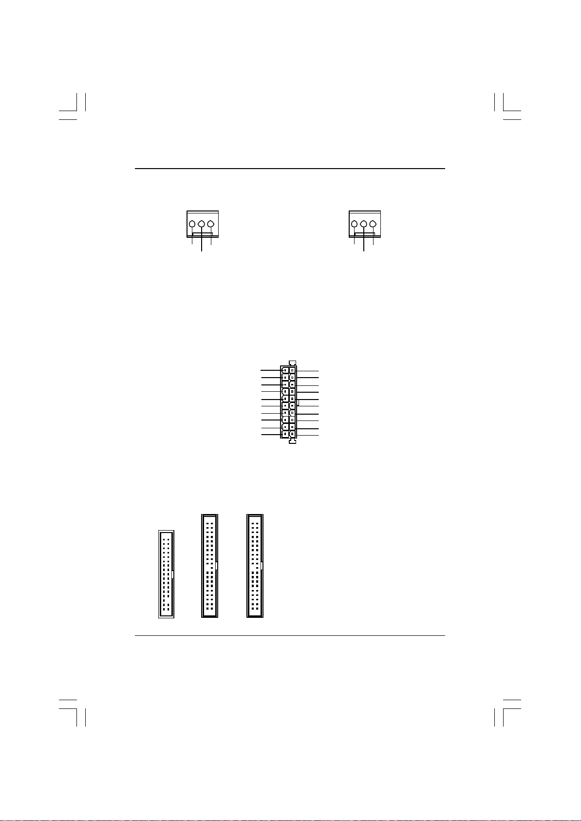
第一章 序言
特色彙總
規格 l 主機板採四層設計 ATX 規格 30.5公分x 23.5公分
主機板 l GA-7VRX/GA-7VRXP主機板
中央處理器 l AMD AthlonTM / AthlonTM XP / DuronTM (K7) Socket A處理器
128K 第一層快取記憶體及256K/64K 第二層快取記憶體
內含於CPU
支援 1.4 GHz以上或更快
l 系統匯流排支援200/266 MHz FSB
晶片組 l VIA KT333 Memory/AGP/PCI北橋控制晶片
l VT8233A(CE)南橋控制晶片
記憶體 l 3 184-pin DDR DIMM 插槽
l 支援PC1600/PC2100/PC2700 DDR DRAM
l 支援only 2.5V DDR DIMM
l 最大支援到3.0GB DDR
I/O控制器 l IT8705
擴充槽 l 1 個AGP擴充槽,支援4倍 /2倍及AGP2.0相容
l 5 PCI擴充槽支援33MHz及PCI2.2 compliant
內建IDE l 2 IDE bus master (ATA 66/100/133) IDE埠可連接4 ATAPI裝置
l IDE3及IDE4適用於RAID, Ultra ATA-133/100,EIDE.
內建周邊設備 l 1個軟碟插座支援兩台磁碟機 (360K,720K,1.2M,1.44M
及2.88M bytes)
l 1組並列埠插座可支援Normal/EPP/ECP模式
l 2組串列埠插座(COM A & COM B)
l 4 組通用串列埠排線 x 1 (USB 2.0) ,
2組通用串列埠排線x 1 (USB 1.1) 及內建2組 USB 1.1
l 1個紅外線連接端
<註 1>
序言
<註 1> 因為 PC2700 記憶體模組有多種款式,所以我們不建議您同時使用
三隻 PC2700 的記憶體模組.
續下頁.......
9
Page 10

GA-7VRX/GA-7VRXP主機板
硬體監控 l CPU /系統風扇運轉偵測
l CPU /系統風扇溫度偵測
l 系統電壓自動偵測
內建網路晶片* l 內建RTL8100BL晶片
內建音效晶片 l 內建CT5880音效晶片*
l 內建Sigmatel9721T CODEC 音效晶片
l Line In/Line Out/Mic In/CD In/Game Port
內建RAID功能* l Promise PDC20276
l 支援資料striping (RAID 0) or mirroring (RAID 1)
l 支援雙IDE通道並行作業
l 符合IDE bus master標準
l 開機時顯示狀態及錯誤檢查訊息
l Mirroring 功能支援自動背景重建
l 內建的BIOS具備LBA 與延伸中斷13h磁碟機容量轉換
內建USB2.0 l VIA VT6202
內建MS,SD,SC* l Winbond SMART @I/O晶片(Memory Stick,Security Digital
and SC header)
PS/2插座 l PS/2鍵盤插座及PS/2滑鼠插座
BIOS l 使用經授權AMI BIOS,2M bit快閃記憶體
l 支援雙BIOS (Dual BIOS)
l 支援Q-Flash
附加特色 l 網路喚醒功能 (WOL)
l 支援@BIOS
TM
l 支援Easy Tune TM4
M 請依據您CPU 的規格來設定 CPU 的頻率,我們不建議您將系統速度設定超過硬
體之標準範圍,因為這些規格對於周邊設備而言並不算是符合標準規格。如果您
要將系統速度設定超出標準規格 , 請依據您的硬體規格設定,例如;CPU,顯示卡,
記憶體,硬碟來設定。
"*" 只有 GA-7VRXP 才有此功能.
10
Page 11
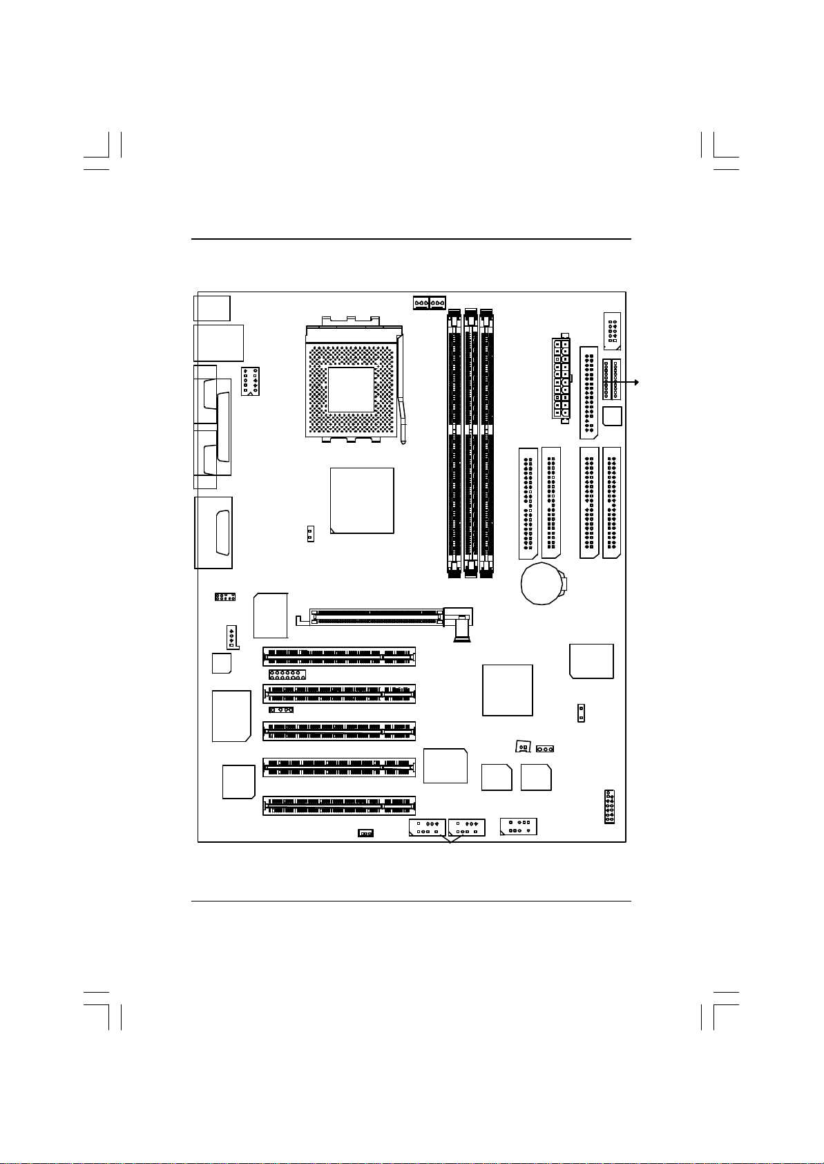
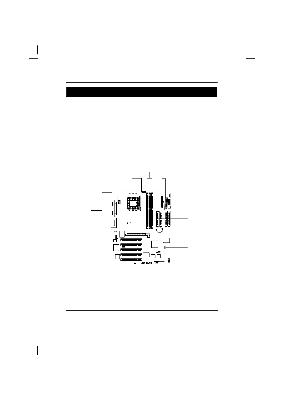
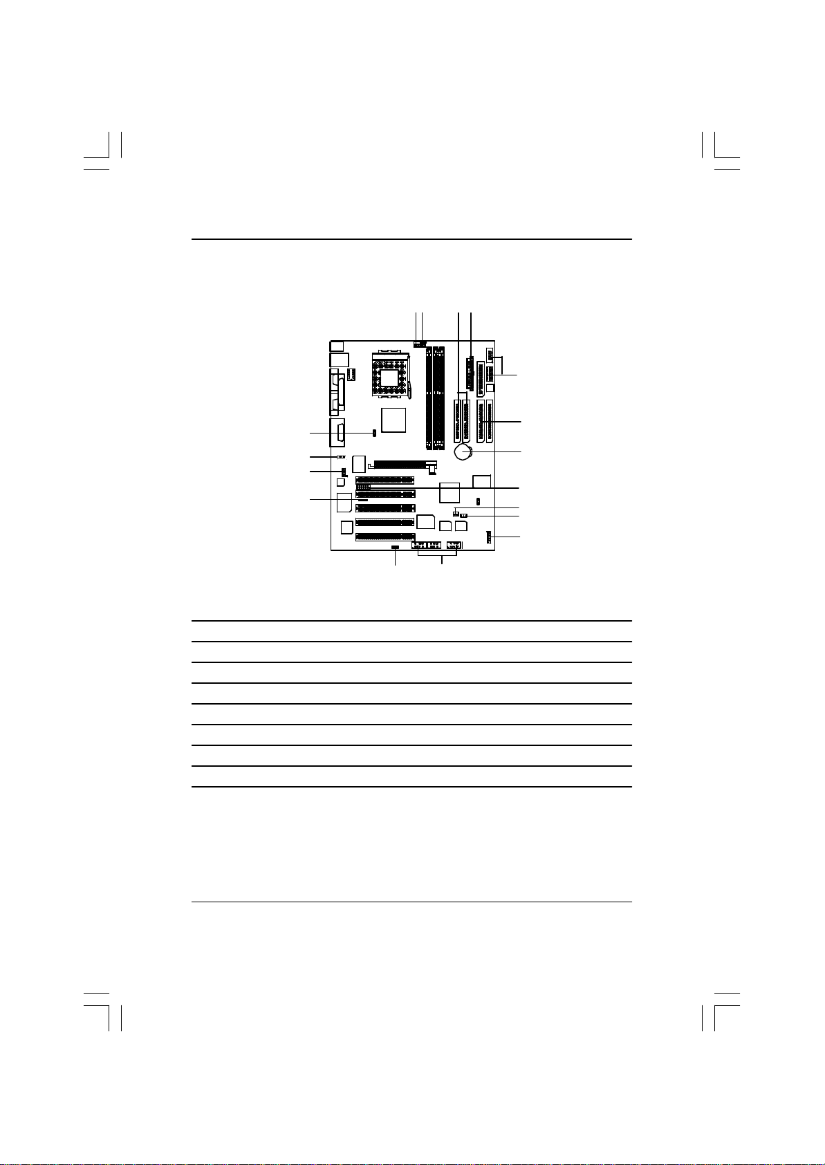
GA-7VRX/GA-7VRXP主機板Layout圖
序言
KB_MS
USB
LAN*
CK_RATIO
COMA
LPTGAM E
SOCKET A
COMB
KT333
LINE_OUT
LINE_IN
MIC_IN
F_AUDIO
CD_IN
AC97
CT5880*
RTL
8100BL*
NB_FAN
AGP
IT8705
SC**
IR
WOL
"*" 只有 GA-7VRXP 才有此功能.
SYS
CPU
FAN
FAN
GA-7VRX / GA-7VRXP
DDR1
DDR2
DDR3
PCI1
PCI2
PCI3
PCI4
VIA VT6202
PCI5
USB 2.0
VT8233ACE
#CI
MAIN
BIOS
F_USB3F_USB4
F_USB1
"**" 只有 GA-7VRX 才有此功能.
"#" 只有 PCB Ver. 1.1 的 GA-7VRX/GA-7VRXP 才有此功能.
IDE1
BATTERY
Backup
BIOS
ATX
IDE2
SW1
#CLR_CMOS
FLOPPY
IDE4*
PDC20276*
F_PANEL
W83
L518D
IDE3*
SC*
SD*
MS*
11
Page 12
GA-7VRX/GA-7VRXP主機板
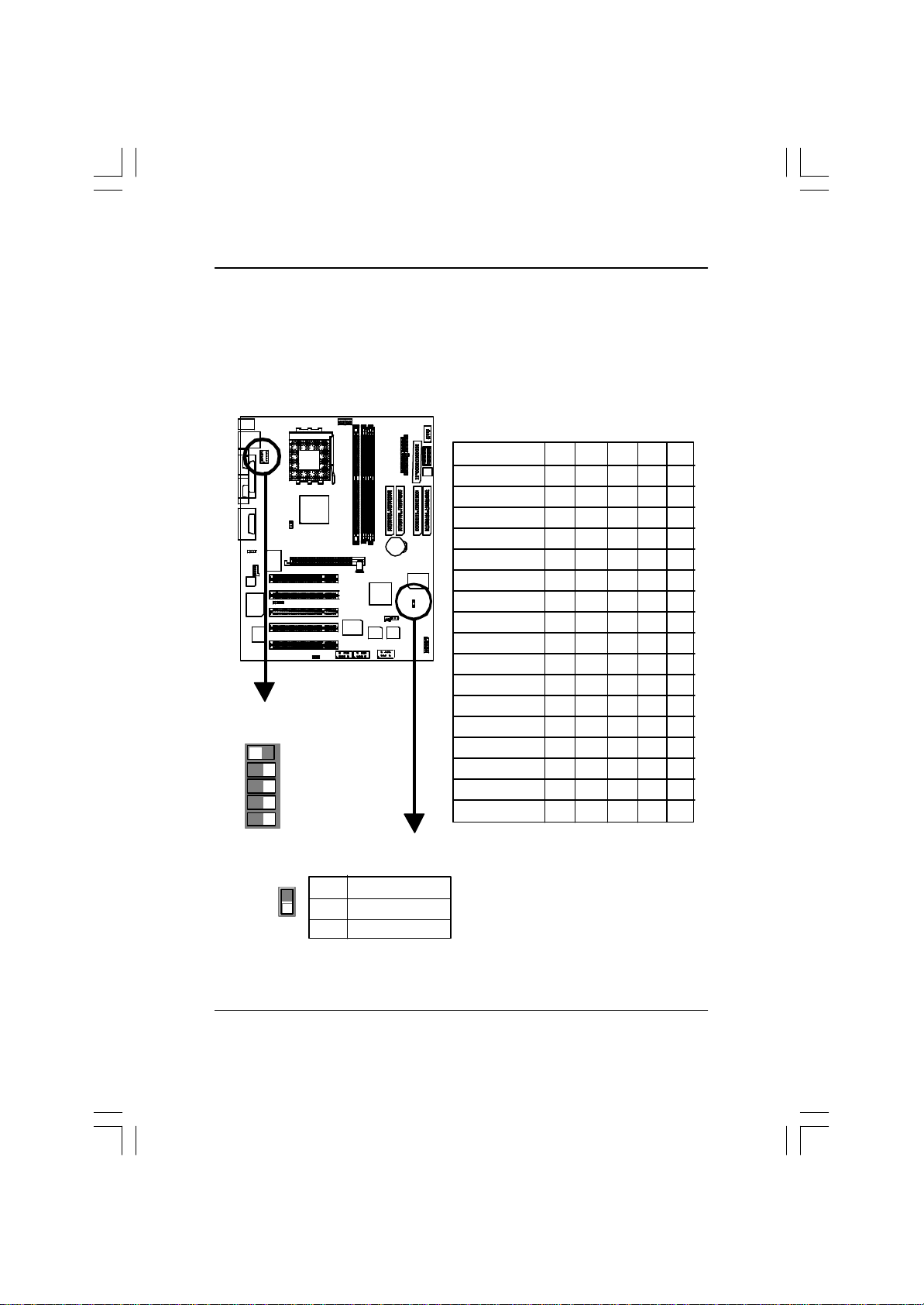
第二章 硬體安裝步驟
請依據下列方式,完成電腦的安裝:
步驟 1 - 設定Dip Switch (CK_RATIO)及系統Switch (SW1)
步驟 2 - 安裝中央處理器 (CPU)
步驟 3 - 安裝記憶體模組
步驟 4 - 安裝所有介面卡
步驟 5 - 連接所有訊號線、排線、電源供應線及面板控制線
步驟 6 - 完成 BIOS 組態設定
步驟 7 - 安裝軟體驅動程式
步驟 5
步驟 4
步驟 1
步驟 2 步驟 3 步驟 5
步驟 5
步驟 1
步驟 5
12
Page 13
硬體安裝步驟
步驟1:安裝中央處理器(CPU)
步驟1-1: 中央處理器速度設定
CPU 倍頻選擇可參考以下表格, 您可以選擇由Dip Switch(CK_RATIO) 來調整CPU 倍
頻。
O: ON / X :OFF
RATIO 1 2 3 4 5
AUTO(預設值) X X X X O
5x O O X O X
5.5x X O X O X
6x O X X O X
6.5x X X X O X
7x O O O X X
7.5x X O O X X
8x O X O X X
8.5x X X O X X
9x O O X X X
9.5x X O X X X
預設值 : Auto
(X X X X O)
ON
CK_RATIO
ON
SW1
5
2 3 4
1
1
SW1 CPU CLOCK
ON 100MHz (預設值)
OFF 133MHz
O: ON / X :OFF
10x O X X X X
10.5x X X X X X
1 1x O O O O X
1 1.5x X O O O X
12x O X O O X
>=12.5x X X O O X
系統速度可以選擇設定為100 ,133MHz。
您可以選擇由Switch (SW1) 來調整系統
速度。(內部頻率選擇取決於CPU)
13
Page 14
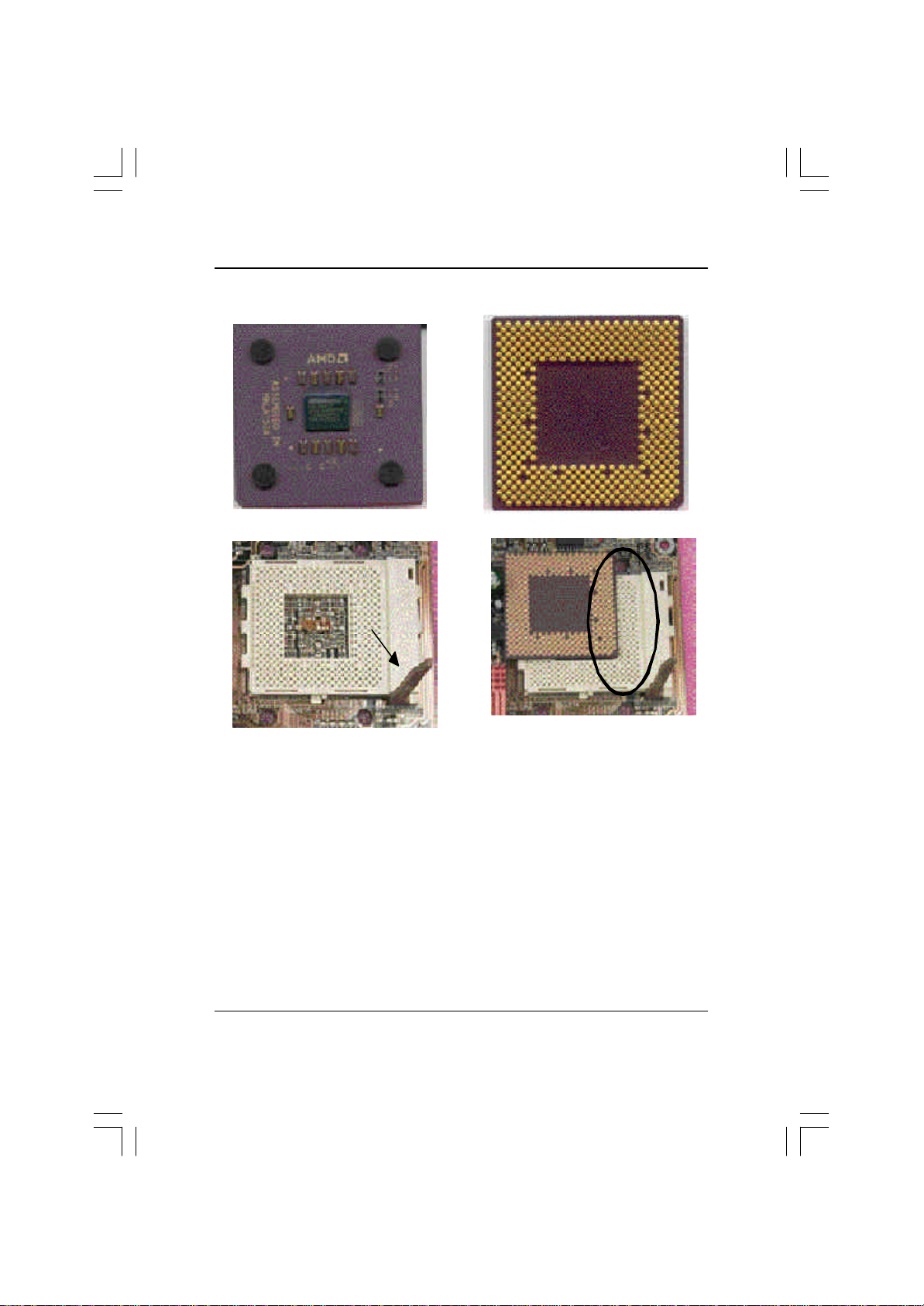
GA-7VRX/GA-7VRXP主機板
步驟1-2:中央處理器之安裝
中央處理器正面
連桿
1.將處理器插座連桿向上拉起
至90度角的位置.
中央處理器背面
斜腳
2. 將處理器的斜腳對準插座上的
斜腳後, 將處理器平行插入插座.
M 請確認您使用的中央處理器為本主機板的支援範圍。
M C PU 的第一腳位置,若您插入的方向錯誤,處理器就無法插入,
請立刻更改插入方向。
14
Page 15
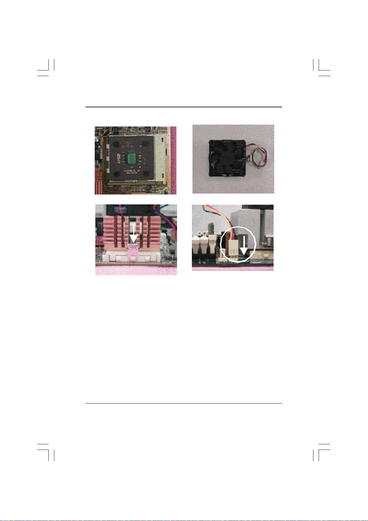
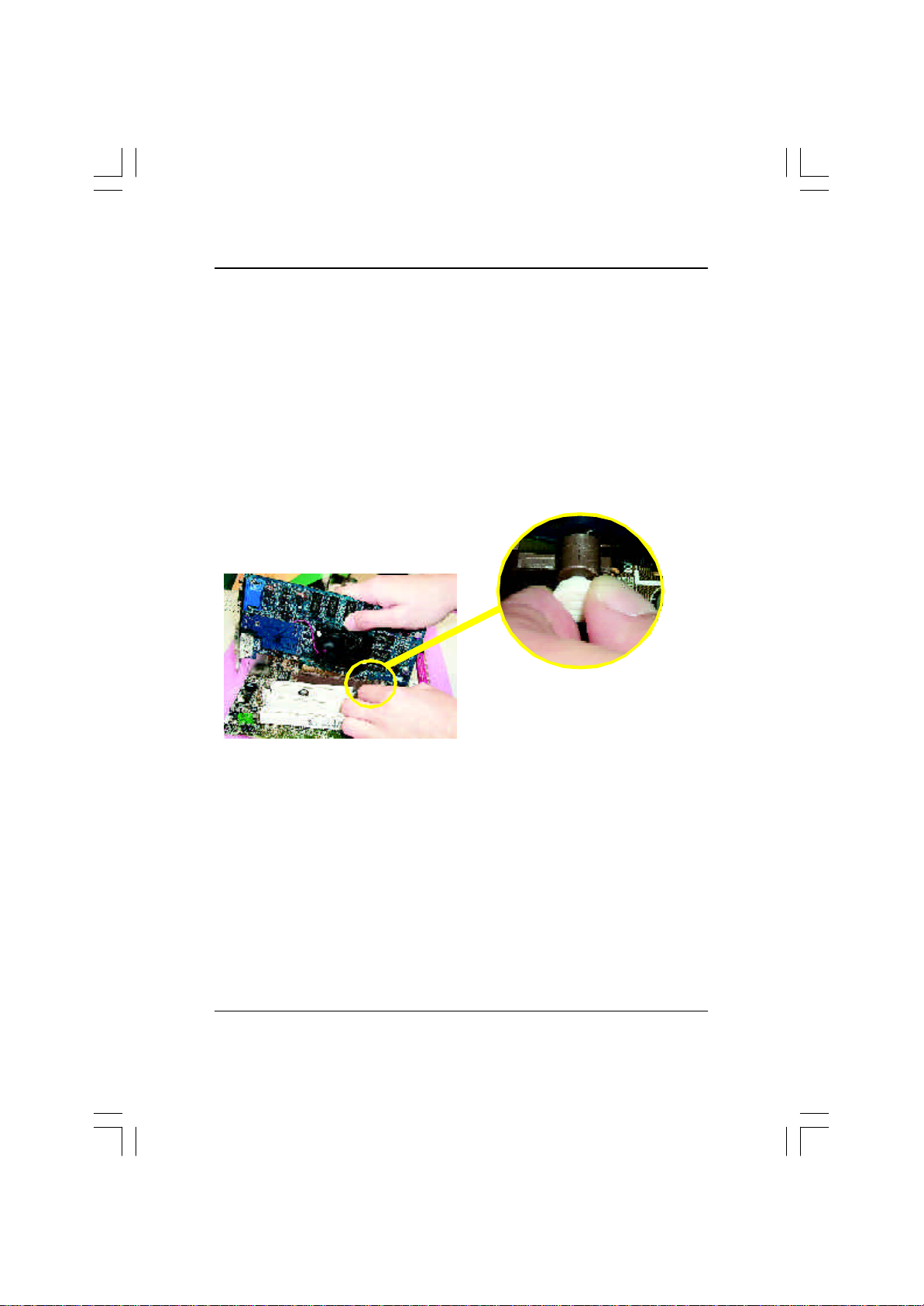
步驟1-3:中央處理器之散熱裝置安裝
硬體安裝步驟
1. 將連桿往下按至原位
3. 先將CPU 散熱風扇一邊的
卡榫以平均施力的方式往
下壓,直至扣緊為止;以同樣
地方式再將另一邊卡榫扣
緊.
2. 使用經AMD認證過的散熱風扇
4. 將CPU 散熱風扇的電源線
插入主機板上的 CPU FAN
插座,即安裝完成.
M 使用經AMD 認證過的散熱風扇。
M CPU 與風扇之間建議黏上散熱膏以增強散熱效果。
M 依您實際所使用的散熱風扇,以正確方向將風扇確實扣緊。
M 確認 CPU 散熱風扇電源線接至 CPU F AN 接頭,完成安裝。
(詳細安裝步驟請參考散熱風扇的使用手冊)
15
Page 16

GA-7VRX/GA-7VRXP主機板
步驟2:安裝記憶體模組
此主機板有3個(DIMM)擴充槽,BIOS會自動偵測記憶體的規格及其大小。安裝
記憶體只需將DIMM插入其插槽內即可,由於記憶體模組有一個凹痕,所以只能以
一個方向插入。在不同的插槽,記憶體大小可以不同。確認您所購買的記憶體模組
適用本主機板所支援的規格。
使用 Registered / Unbuffered DDR DIMM 時的總記憶容量(不支援ECC 功能)
Devices used on DIMM 1 DIMMx64/x72 2 DIMMsx64/x72 3 DIMMsx64/x72
64 Mbit (2Mx8x4 banks) 128 MBytes 256 MBytes 384 MBytes
64 Mbit (1Mx16x4 banks) 64 MBytes 128 MBytes 192 MBytes
128 Mbit(4Mx8x4 banks) 256 MBytes 512 MBytes 768 MBytes
128 Mbit(2Mx16x4 banks) 128 MBytes 256 MBytes 384 MBytes
256 Mbit(8Mx8x4 banks) 512 MBytes 1 GBytes 1.5 GBytes
256 Mbit(4Mx16x4 banks) 256 MBytes 512 MBytes 768 MBytes
512 Mbit(16Mx8x4 banks) 1 GBytes 2 GBytes 3 GBytes
512 Mbit(8Mx16x4 banks) 512 MBytes 1 GBytes 1.5 GBytes
16
Page 17

硬體安裝步驟
DDR
1 .記憶體模組有一個凹痕,所以只能以一個方
向插入。
2.確認DIMM 記憶體模組安裝於 DIMM 插槽內,
然後下壓。
3.將卡楯向內推,確實卡住記憶體模組
DIMM 。一旦固定位置,兩旁的卡楯便自動
卡住記憶體模組予以固定。試著輕輕搖動記
憶體模組,若不搖晃則裝置成功。
M 當您要移除DIMM 記憶體模組,請反向操作以上步驟。
DDR 功能介紹
DDR(Double Data Rate)是PC 產業在SDRAM 架構上的一項重要演進,利用雙倍的
記憶體頻寬可解決系統資料的瓶頸問題。建立在SDRAM 的基礎架構設計之上,
DDR是一項高效能及低成本兼具的創新技術,能使記憶體廠商、 OEM系統廠商在熟
悉的標準上建構新一代的電腦系統產品。
因為具有優良可行性、價格以及整體市場的支援性,DDR SDRAM將提供優良的
解決方式以及將現有的SDRAM轉換到DDR SDRAM 的最佳路徑。
DDR可雙倍讀與寫的資料傳輸速率,利用最高可達2.1GB/s的傳輸速度,DDR能
使系統廠商建立一個高效能及低滯留時間的DRAM架構,適合在伺服器、工作
站、高階PC以及進階整合性電腦系統使用。相對於目前SDRAM 的3.3 volts 高核心
電壓,DDR的2.5 volts超低核心電壓將使得 DDR為小型規格的桌上電腦以及筆記型
電腦的最佳技術解決方案。
M 記憶體模組設計有防呆標示,若您插入的方向錯誤, 記憶體模
組就無法插入,請立刻更改插入方向
M 當 STR/L ED 燈指示燈在亮的狀態時,請勿插拔 DDR.
17
Page 18
GA-7VRX/GA-7VRXP主機板
步驟3:安裝介面卡
1. 在安裝介面卡之前請先詳細閱讀介面卡之使用手冊並將您電腦的電源關掉。
2. 將您電腦外殼拆除,並且讓自己保持接地。(為了使人體不帶電,以防止靜電傷
害電腦設備)。
3. 鬆開螺絲,移開介面卡安裝擴充槽旁的金屬擋片。
4. 將介面卡小心且確實的插入在擴充槽中。
5. 請確定所有介面卡皆確實固定插在該擴充槽,並將螺絲鎖回。
6. 重新將電腦機殼蓋上。
7. 接上電源線,若有必要請至BIOS程式中設定介面卡之相關設定。
8. 安裝相關驅動程式。
當您要安裝/移除AGP卡時,請將白
色拉桿向外拉. 再將AGP卡緩緩插
入AGP擴充槽中. 放開拉桿 確實卡
AGP 卡
住AGP卡
18
Page 19
硬體安裝步驟
步驟4:連接所有訊號線、排線、電源供應線及面
板控制線
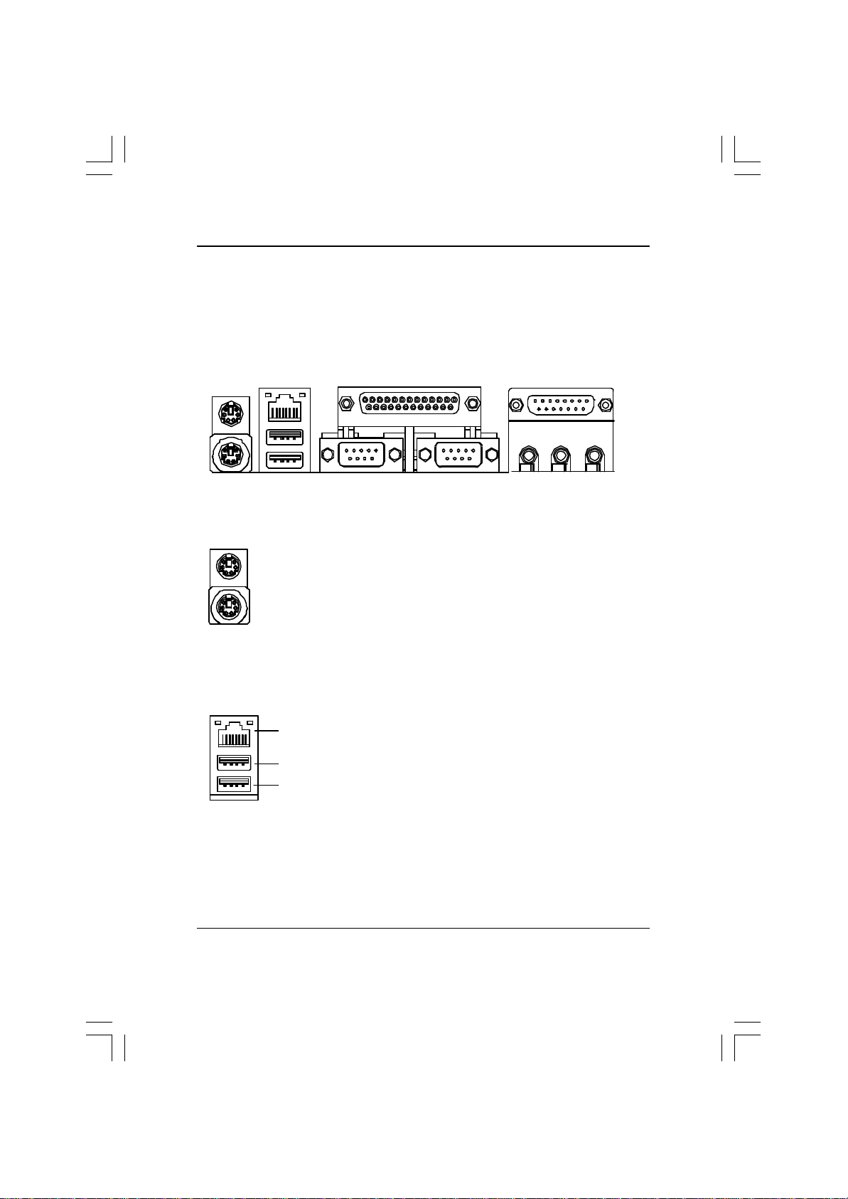
步驟4-1:後方I/O裝置插座介紹
u
v
w
x
y
u PS/2 Keybo ard / Mouse (PS/2 鍵盤及 PS/2 滑鼠插座)
PS/2 Mouse (PS/2滑鼠插座)
(6 pin Female)
PS/2 Keyboard (PS/2鍵盤插座)
(6 pin Female)
Ø 本主機板提供標準PS/2鍵盤介面及
PS/2滑鼠介面插座。
v USB / LAN Conn ector (LAN 通用序列埠, 網路插座)
LAN Connector (網路插座)*
USB0 (通用序列埠 0)
USB1 (通用序列埠1)
Ø當你要使用通用串列埠連接埠時,必須
先確認您要使用的週邊裝置為標準的
USB介面,如:USB鍵盤,滑鼠,USB
掃瞄器,USB ZIP ,USB 喇叭等….而且
您也必須確認您的作業系統是否有支援
此功能,或是需要另外再掛其他的驅動
程式,如此才能正常工作,詳情請參考
USB週邊裝置的使用手冊。
"*" 只有 GA-7VRXP 才有此功能.
19
Page 20
GA-7VRX/GA-7VRXP主機板
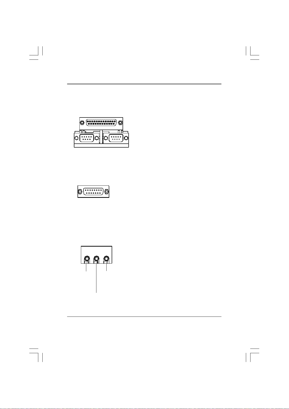
w COMA(串列埠 A)/ COMB ( 串列埠 B)/LPT(印表機並列埠插座)
LPT Port
並列埠插座
(25 pin Female)
Ø本主機板支援二組標準的串列埠傳輸協
定之週邊裝置、一組標準的並列傳輸協
定之週邊裝置,您可以依據您的需求連
接您需要的裝置,如並列埠有印表機,
串列埠有滑鼠、數據機等。
COMA
串列埠A
(9 pin Male)
COMB
串列埠B
x GAME/MID I Ports (遊戲搖桿控制埠)
Ø本主機板支援標準的音效輸入接腳及遊
GAME/MIDI
遊戲搖桿控制埠
(15 pin Female)
y Aud io Connector (音源插座)
Ø 麥克風接腳可接在麥克風輸入端,至於
LINE OUT
類比音源
訊號輸出
MIC IN
麥克風輸入
戲搖桿控制埠,您在設定完成內建音效
的驅動程式後,即可將喇叭輸出接腳接
在音源輸出端。
音源輸入端可以接上如:光碟機,隨身
聽及其他音源輸入接腳。
LINE IN
類比音源
訊號輸入
20
Page 21
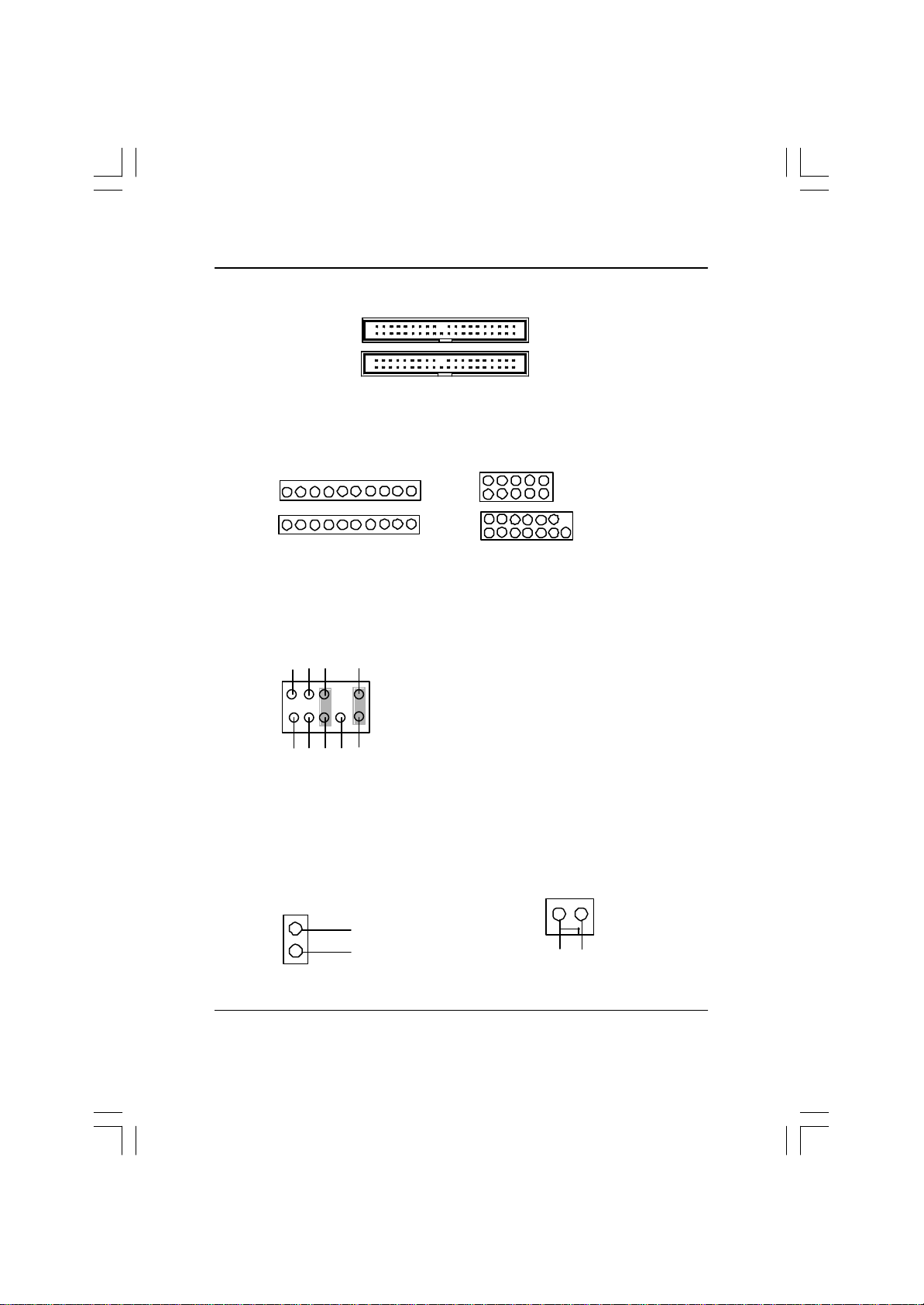
步驟4-2:插座介紹
硬體安裝步驟
AB C
D
P
O
N
M
L
K
A) CPU FAN I) CLR_C MOS#
B) SYS FAN J) F_Panel
C) Floppy/IDE1/IDE2 K) F_USB 1,3,4
D) ATX L) WOL
E/E1)SC/SD/MS* / SC** M) IR
F) IDE3/IDE4* N) CD_IN
G) Battery O) F_AUDIO
H) CI# P) NB_FAN
E
F
G
E1
#H
#I
J
"*" 只有 GA-7VRXP 才有此功能.
"**" 只有 GA-7VRX 才有此功能.
"#" 只有 PCB Ver. 1.1 的 GA-7VRX/GA-7VRXP 才有此功能.
21
Page 22
GA-7VRX/GA-7VRXP主機板
A) CPU_FAN
( CPU 散熱風扇電源插座)
1
訊號線
接地線
+12V/Control
Ø 此CPU 散熱風扇電源插座, 提供最大
電流為600毫安培.
B) SYS_FAN
(系統散熱風扇電源插座)
1
訊號線
接地線
+12V/Control
D) ATX ( ATX Power 電源插座)
20
5V SB (Stand by +5V)
Ø 請特別注意,先將AC 交流電(110/220V)拔除,再將ATX電源插頭緊密的插入
主機板的ATX電源插座,並接好其相關配備才可以將AC交流電(110/220V)插
入交流電源插座。
+12V
電源良好
接地線
VCC
接地線
VCC
接地線
3.3V
3.3V
1
VCC
VCC
-5V
接地線
接地線
接地線
PS-ON(Soft On/Off)
接地線
-12V
3.3V
C) FDD / IDE1 / IDE2 (軟碟機插座 / 第一組 /第二組硬碟插座)
Ø 請特別注意:
請將您的第一顆硬碟連接第一組IDE
FDD
IDE1
1
IDE2
1
1
插座.光碟機接至第二組IDE插座.
22
Page 23
K ) US B1,3,4 ( 前端通用串列埠插座,橘色插座為 USB2.0)
Ø 請特別注意,前端USB接腳是有方
USB Dx+
無作用
接地線
電源
USB Dx-
USB Dx-
USB Dx-
電源
無作用
接地線
向性的,所以安裝USB裝置時,要
特別注意極性,而且前端USB連接
排線為選擇性的功能套件,可以聯絡
相關代理商購買。
M ) IR ( 紅外線插座)
1
IRTX
IRRX
VCC
無作用
接地線
Ø 請特別注意,紅外線接腳是有方向性
的,所以在安裝紅外線裝置時,要特
別注意極性,而且紅外線裝置為選擇
性的功能套件,可以聯絡相關代理商
購買。
硬體安裝步驟
N ) CD _I N( 光碟機音源插座)
右聲道音源輸入
接地線
1
左聲道音源輸入
G) Batt ery (電池)
+
L ) WOL (網路卡喚醒功能插座)
+5V SB
接地線
訊號線
1
警告
v如果電池有任何不正確的移除動作,
將會產生危險。
v 如果需要更換電池時請更換相同廠
牌、型號的電池。
v有關電池規格及注意事項請參考電池
廠商之介紹。
23
Page 24
GA-7VRX/GA-7VRXP主機板
F ) ID E3 / IDE4 Connector (RAID 及 ATA-133 插座)
IDE4
IDE3
1
E/E1) SC (Smart Card Interface), SD (Secure Digital Memory Card Interface) ,
MS (Memory Stick Int erface)
1
O ) F_AUDIO (第二組音源插座)
Rear Audio (R)
接地線MIC
電源線
2
1
REF
Rear Audio (L)
10
9
保留
Front Audio (L)
Front Audio (R)
P ) N B_FAN
1
訊號線
接地線
SD
1
MS1
1
Ø 請特別注意,當您購買電腦機殼
時,可以選購音效接腳是設計在電
腦機殼的前面面板上,此時就可以
使用第二組音源接腳,如果有任何
問題可能就近向經銷商詢問相關問
題。注意:若您要使用第二組音源接
腳,請移除Pin5-6,Pin9-10 的
Jumper。
SC (2x5pin--7VRXP)
5
7
H ) CI (C ASE OPEN)
只有 PCB Ver. 1.1 的 GA-7VRX/
GA- 7VRXP 才有此功能.
SC (2x7pin--7VRX)
1
訊號線
接地線
24
Page 25
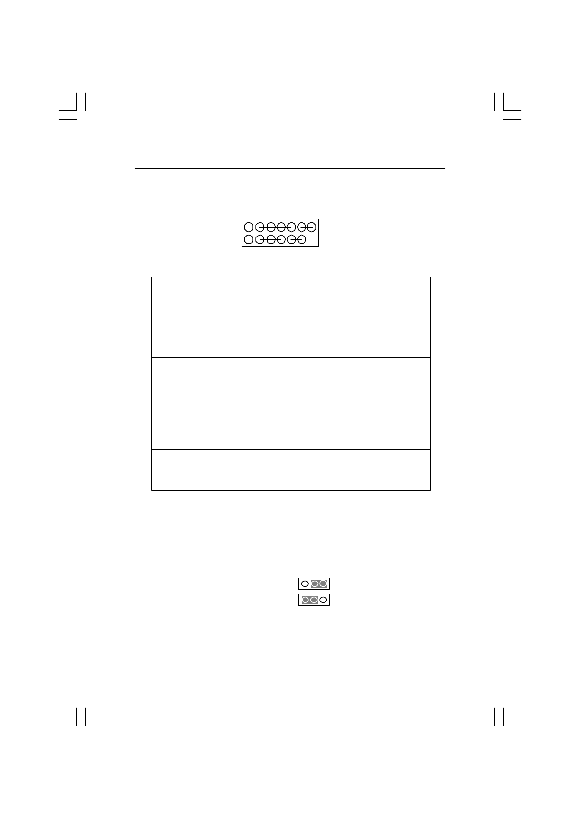
J ) F_PANEL( 2X7 前端控制面板跳線)
硬體安裝步驟
HD-
SPK-
2 14
1
1
HD+
PD_Y
PD_G
HD (IDE Hard Disk Active LED) Pin 1: LED anode(+)硬碟指示燈正極
硬碟動作指示燈 Pin 2: LED cathode(-)硬碟指示燈負極
SPK (Speaker Connector)喇叭接腳 Pin 1: VCC(+) +5v 電源接腳
RST (Reset Switch)系統重置開關 Open: Normal Operation 一般運作
PD+/PD_G/PD_Y (Power LED) Pin 1: LED anode(+) 電源指示燈正極
電源指示燈 Pin 2: LED cathode(-)電源指示燈負極
PW (Soft Power Connector) Open: Normal Operation 開路:一般運作
按鍵開關機 Close: Power On/Off 短路:開機/關機
RST+
RST-
SPK+
1
13
PW-
PW+
PD+
M 請注意正負極性
Pin 2- Pin 3: NC 空腳
Pin 4: Data(-) 訊號接腳
Close: Reset Hardware System
強迫系統重置開機
M 無正負極性正反皆可使用
Pin 3: LED cathode(-)電源指示燈負極
M 無正負極性正反皆可使用
Ø 請特別注意,當您購買電腦機殼時,電腦機殼的控制面板有電源指示燈
,喇叭,系統重置開關,電源開關等,你可以依據上列表格的定義加上
連接。
I) CLR_CMOS: 清除 CMOS
1-2 短路:清除 CMOS
只有 PCB Ver. 1.1 的 GA-7VRX/
GA-7VRXP 才有此功能.
25
1
2-3 短路: 一般運作(預設值)
1
Page 26

GA-7VRX/GA-7VRXP主機板
第三章 BIOS 組態設定
基本上主機板所附AMI BIOS便包含了CMOS SETUP程式,以供使用者自行依照需
求,設定不同的數據,使電腦正常工作,或執行特定的功能。
CMOS SETUP會將各項數據儲存於主機板上內建的 CMOS SRAM中,當電源關閉時,
則由主機板上的鋰電池繼續供應CMOS SRAM 所需電力。
當電源開啟之後,BIOS開始進行POST(Power On Self Test開機自我測試)時,按
下<Del>鍵便可進入AMI BIOS 的CMOS SETUP主畫面中。如果您需要進階的BIOS
設定,當您在BIOS設定畫面時按下“Ctrl+F1”即可進入。
如果您來不及在POST過程中按下<Del>鍵順利進 CMOS S ETUP ,那麼可以補按
<Ctrl>+<Alt>+<Del >暖開機或按下機殼上的Reset按鈕,以重新開機再次進
POST程序,再按下<Del>鍵進入CMOS SETUP 程式中。
操作按鍵說明
h 移到上一個項目
i 移到下一個項目
f 移到左邊的項目
g 移到右邊的項目
Enter 確定選項
Esc 回到主畫面,或從主畫面中結束SETUP程式
Page Up 改變設定狀態,或增加欄位中之數值內容
Page Down 改變設定狀態,或減少欄位中之數值內容
F1 可顯示目前設定項目的相關說明
F2 功能保留
F3 功能保留
F4 功能保留
F5 可載入該畫面原先所有項目設定(但不適用主畫面)
F6 可載入該畫面之Fail-Safe預設設定(但不適用主畫面)
F7 可載入該畫面之Optimized預設設定(但不適用主畫面)
F8 Dual BIOS/ Q-Flash功能
F9 系統資訊
F10 儲存設定並離開CMOS SETUP 程式
26
Page 27

BIOS組態設定
如何使用輔助說明
主畫面的輔助說明
當您在SETUP主畫面時,隨著選項的移動,底下便跟著顯示︰目前被選到的
SETUP項目的主要設定內容。
設定畫面的輔助說明
當您在設定各個欄位的內容時,只要按下<F1>,便可得到該欄位的設定預設值
及所有可以的設定值,如BIOS 預設值或 CMOS SETUP 預設值,若欲跳離輔助說明
視窗,只須按<Esc>鍵即可。
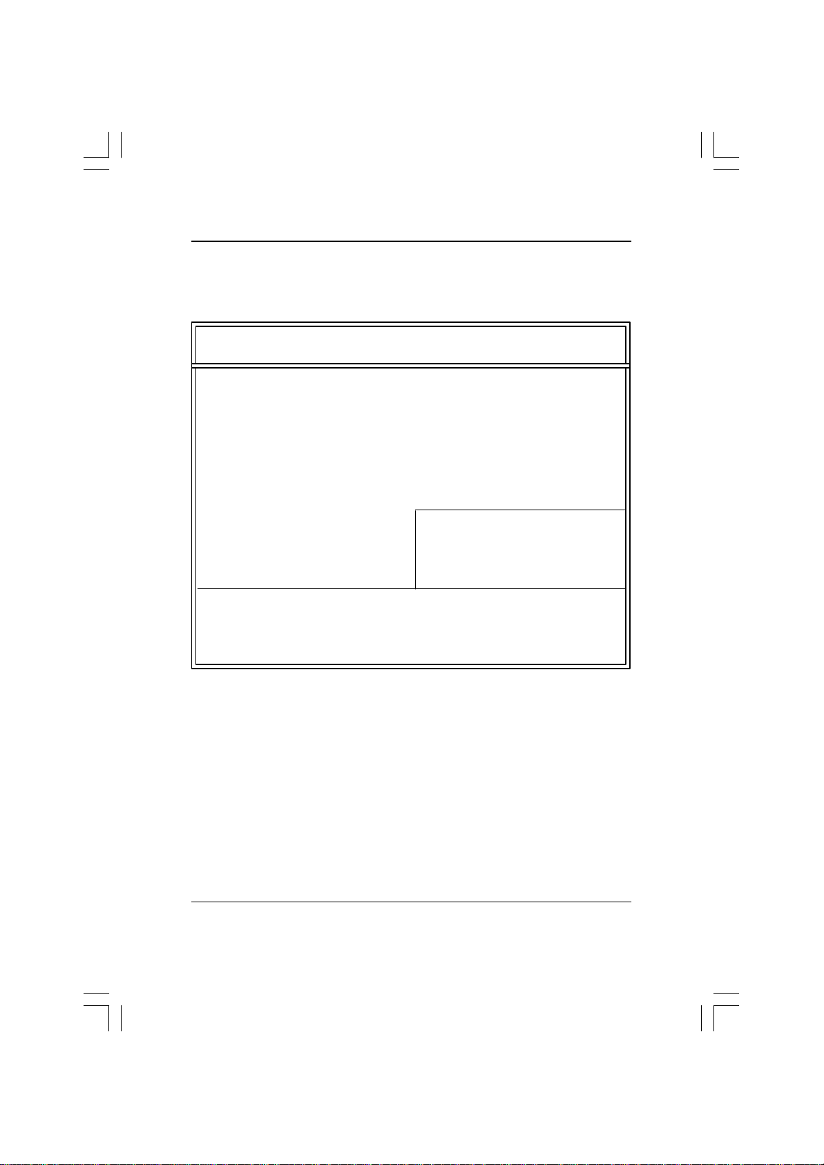
主畫面功能 (BIOS 範例版本 --7VRXP: F8)
當您進入CMOS SETUP設定畫面時,便可看到如下之主畫面,從主畫面中可以讓你
選擇各種不同之設定選單,你可以用上下左右鍵來選擇你要設定之選項並按Enter
進入子選單。
AMIBIOS SIMPLE SETUP UTILITY - VERSION 2.00
(C) 2001 American Megatrends, Inc. All Rights Reserv ed
STANDARD CMOS SETUP INTEGRATED PERIPHERALS
BIOS FEATURES SETUP HARDWARE MONITOR & MISC SETUP
CHIPSET FEATURES SETUP SUPERVISOR PASSWORD
POWER MANAGEMENT SETUP USER PASSWORD
PNP / PCI CONFIGURATION IDE HDD AUTO DETECTION
LOAD FAIL-SAFE DEFAULTS SAVE & EXIT SETUP
LOAD OPTIMIZED DEFAULTS EXIT WITHOUT SAVING
ESC: Quit hifg: Select Item F5: Old Values F6: Fail-Safe Values
F7: Optimized Values F8:Dual BIOS/Q-Flash F10:Sav e & Exit
Time, Date , Hard Disk Ty pe…
圖 1: 主畫面功能
l Stand ard CMOS Features (標準 CMOS 設定)
設定日期、時間、軟硬碟規格、及顯示器種類。
l BIOS Features Setup (BIOS 功能設定)
設定BIOS提供的特殊功能,例如病毒警告、開機磁碟優先程序、磁碟代號交
換....等。
27
Page 28

GA-7VRX/GA-7VRXP主機板
l Chip set Features Setup (晶片組特性設定)
設定主機板採用的晶片組相關運作參數,例如「DRAM Timing」、「ISA Clock」....
等。
l Power Manag ement Setup (省電功能設定)
設定CPU 、硬碟、 GREEN 螢幕等裝置的省電功能運作方式。
l PNP/PCI Confi guration (即插即用與 PCI 組態設定)
設定ISA之PnP即插即用介面以及 PCI介面的相關參數。
l Load Fail-Safe Defaults(載入 Fail-Safe 預設值)
執行此功能可載入BIOS 的CMOS設定預設值,此設定是比較保守,但較能進
入開機狀態的設定值。。
l Load Op timized Defaults(載入 Optimized 預設值)
執行此功能可載入Optimized的CMOS 設定預設值,此設定是較能發揮主機
板速度的設定。
l Integ rated Peripherals (內建整合週邊設定)
在此設定畫面包括所有週邊設備的的設定。如COM Port 使用的IRQ 位 址,
LPT Port 使用的模式SPP、EPP或 ECP以及IDE 介面使用何種PIO Mode 等裝
置之設定。
l H ar dw are Moni tor & MISC Setup (硬體監視設定)
自動偵測風扇及系統溫度功能。
l Supervi sor Pass w ord (管理者的密碼)
設定一個密碼,並適用於進入系統或進入SETUP修改CMOS 設定。
l U ser Password (使用者的密碼)
設定一個密碼,並適用於開機使用PC及進入BIOS 修改設定 。
l IDE H DD Auto Dete ction (自動偵測 IDE硬碟)
自動偵測IDE的參數設定,並可選擇寫入CMOS(記得要存檔)。
l Save & Exit Setup (儲存並結束)
儲存所有設定結果並離開SETUP程式,此時BIOS 會重新開機,以便使用新
的設定值,按<F10>亦可執行本選項。
l Exit Without Saving (離開 CMOS 不儲存設定)
不儲存修改結果,保持舊有設定並重新開機,按 <ESC>亦可直接執行本選項。
28
Page 29
BIOS組態設定
標準 CMOS 設定
在STANDARD CMOS SETUP 中,主要是為了設定IDE硬碟的種類,以順利開機,除
此之外,還有日期、時間、軟碟規格、及顯示卡的種類可以設定
AMIBIOS SETUP - STANDARD CMOS SETUP
( C ) 2001 American Megatrends, Inc. All Rights Reserv ed
Date (mm/dd/y yyy) : Fri Mar 16, 2001
Time (hh/mm/ss) : 14:44:35
TYPE SIZE CYLS HEAD PRECOMP LANDZ SECTOR MODE
Pri Master : Auto
Pri Slav e : Auto
Sec Master : Auto
Sec Slav e : Auto
Floppy Drive A : 1.44 MB 3
Floppy Drive B : Not Installed Other Memory : 384 Kb
Boot Sector Virus Protection : Disabled Total Memory : 256 Mb
Month : Jan - Dec ESC : Ex it
Day : 01- 31 hi : Select Item
Year : 1990 - 2099 PU / PD / + / - :Modify
1/2
圖 2: 標準 CMOS設定
Base Memory : 640 Kb
Ex tended Memory : 255 Mb
(Shift) F2 : Color
CDate(mm:dd :yy) (日期設定)
即設定電腦中的日期,格式為「星期,月/日/年」,各欄位設定範圍如下
表示:
8 星期 由目前設定的「月/日 /年」自萬年曆公式推算出今天為星期幾,此
欄位無法自行修改.
8 月(mm) 1到12 月.
8 日(dd) 1到28/29/30/31 日,視月份而定.
8 年(yy) 1990到2099 年.
29
Page 30

GA-7VRX/GA-7VRXP主機板
CTi me(hh:mm:ss) (時間設定)
即設定電腦中的時間是以24 小時為計算單位,格式為「時:分:秒」舉例而
言,下午一點表示方式為13 : 00 : 00。當電腦關機後,RTC 功能會繼續執行,並由
主機板的電池供應所需電力。
CPrimary Master (Slave) / IDE Second ary Master (Slave)
(第一組硬碟 / 第二組硬碟參數設定)
設定第一、二組IDE硬碟參數規格,設定方式有兩種,建議的是設定方式是採方式
1,但經常更換IDE 硬碟的使用者則可採方式2 ,省去每次換硬碟都要重新設定
CMOS的麻煩。
方式1:設成User TYPE ,自行輸入下列相關參數,即CYLS、HEADS、SECTORS、
MODE,以便順利使用硬碟。
方式2:設定AUTO,將TYPE 及MODE皆設定AUTO,讓 BIOS在POST過程中,自
動測試IDE裝置的各項參數直接採用。
8CYLS. Number of cylinders(磁柱的數量).
8HEADS Number of heads(磁頭的數量).
8PRECOMP Write precomp.
8LANDZONE Landing zone.
8SECTORS Number of sectors(磁區的數量).
如果沒有裝設硬碟,請選擇"NONE" 後按<Enter>
CFlop py Drive A / Floppy Drive B (軟式磁碟機 A:/ B:種類設定)
可設定的項目如下表示:
8None沒有安裝磁碟機.
8360K, 5.25 in. 5.25吋磁碟機,360KB容量.
81.2M, 5.25 in. 5.25吋磁碟機,1.2MB容量.
8720K, 3.5 in. 3吋半磁碟機,720KB容量.
81.44M, 3.5 in. 3吋半磁碟機,1.44MB容量.
82.88M, 3.5 in. 3吋半磁碟機,2.88MB容量.
30
Page 31

BIOS組態設定
CBoot Sector Virus Protection (病毒警告)
8Enabled 啟動此功能,當硬碟的啟動磁區或分割區被改寫時,會發出
警告訊息,由使用者決定是否要被寫入。
8Disabled 不啟動此功能。(預設值)
C Memor y(記憶體容量顯示)
目前主機板所安裝的記憶體皆由BIOS之POST(Power On Self Test)自動偵測,並
顯示於STANDARD CMOS SETUP右下方。
Base Memory:傳統記憶體容量
PC 一般會保留640KB容量做為 MS-DOS作業系統的記憶體使用空間。
Extended Memory:延伸記憶體容量
可做為延伸記憶體的容量有多少,一般是總安裝容量扣除掉Base及Other
Memory 之後的容量,如果數值不對,可能是有Module 沒安裝好,請仔細
檢查。
Other Memory:其它記憶體容量
通常是指BIOS從記憶體容量中,取384KB容量,做為 BIOS Shadow功能的
用途(Shadow RAM)。主要是在開機時,BIOS將一些裝置的驅動程式Copy到
DRAM 上面,使BIOS的執行速度提昇,有助 PC 整體的效益。
31
Page 32

GA-7VRX/GA-7VRXP主機板
BIOS 功能設定
AMIBIOS SETUP - BIOS FEATURES SETUP
( C ) 2001 American Megatrends, Inc. All Rights Reserv ed
BIOS Flash Protection : Auto
1st Boot Dev ice : Floppy
2nd Boot Dev ice : IDE-0
3rd Boot Dev ice : CDROM
Floppy Drive Seek : Disabled
BootUp Num-Lock : On
Passw ord Check : Setup ESC: Quit hifg: Select Item
S.M.A.R.T. for Hard Disks : Disabled F1 : Help PU/PD+/-/ : Modify
Interrupt Mode : APIC F5 : Old Values (Shift)F2: Color
F6 : Fail-Safe F7: Optimized
F8 :Dual BIOS/Q-Flash
圖 3: 進階 BIOS 功能設定
CBIOS Flash Protection (BIOS 防寫保護)
8Auto 在開機過程中時,會更新DMI/ESCD。使用本公司的工具程式
更新 BIOS、DMI/ESCD 的時候,系統會自動開啟 FLASH 寫入
權限 (預設值)
8Enabled 在開機過程中時,不會更新DMI/ESCD。開機完後只能用本公
司的工具更新BIOS。
C1st / 2nd / 3rd Boot Device (第一 / 二 / 三開機裝置)
8Floppy 由軟碟機為第一優先的開機裝置。
8CDROM 由光碟機為第一優先的開機裝置。
8Disabled 關閉此功能。
8IDE-0~3 由硬碟機為第一優先的開機裝置。
開機裝置取決在您安裝的設備。
32
Page 33

BIOS組態設定
CFlop py Drive Seek (開機時測試軟碟)
設定在PC開機時,POST程式需不需要對FLOPPY做一次SEEK測試。可設定的
項目為:
8Enabled 要對Floppy做Seek 測試。
8Disabled 不必對Floppy做Seek 測試。(預設值)
CBoot U p Num-Lock (起始時數字鍵鎖定狀態)
8On 開機後將數字區設成數字鍵功能。(預設值)
8Off 開機後將數字區設成方向鍵功能。
CPassw ord Check(檢查密碼方式)
8Always 無論是開機或進入CMOS SETUP均要輸入密碼。
8Setup 只有在進入CMOS SETUP時才要求輸入密碼。(預設值)
欲取消密碼之設定時,只要於SETUP內重新設定密碼時,不要按任何鍵,直接
按<Enter>使密碼成為空白,即可取消密碼的設定。請參考P.50
CS.M .A.R.T. for Hard Disks ( 硬碟自我檢測功能)
8Enabled 啟動硬碟S.M.A.R.T. 的功能。
8Disabled 關閉硬碟 S.M.A.R.T. 的功能。(預設值)
CInterrupt M ode
8APIC 經由IOAPIC產生更多IRQ 給系統使用。(預設值)
8PIC 以傳統方式產生IRQ給系統使用。
注意:當您使用的CPU 有支援 IOAPIC 模式時,BIOS會自動偵測到 IOAPIC模式,
而且在安裝作業系統時,若BIOS 設定成 API C 模式,作業系統會自動安裝為支援
IOAPIC 模式(例如:Windows NT、Windows 2000、Windows XP...等)。此時若將CPU 更
換成不支援IOAPIC模式的型號或將BIOS變更為PIC 模式,此時會無法進入作業系
統。若碰到上述情況,必須重新安裝作業系統。
33
Page 34

GA-7VRX/GA-7VRXP主機板
晶片組的特性設定
AMIBIOS SETUP - CHIPSET FEATURES SETUP
( C ) 2001 American Megatrends, Inc. All Rights Reserv ed
Top Performance :Disabled
Fast Command :Normal
Configure SDRAM by SPD :Enabled
SDRAM Frequency :Auto
SDRAM CAS# Latency :2.5
SDRAM Command Rate :2T Command
AGP Mode :4X
AGP Comp. Driv ing :Auto
Manual AGP Comp. Driv ing :DA
AGP Fast Write :Enabled
AGP Aperture Size :128MB
AGP Read Sy nchronization :Disabled
PCI Delay Transaction :Enabled ESC: Quit hifg: Select Item
USB Controller :All USB Port F1 : Help PU/PD+/-/ : Modify
USB Legacy Support :Disabled F5 : Old Values (Shift)F2: Color
USB Port 64/60 Emulation :Disabled F6 : Fail-Safe F7 : Optimized
F8 :Dual BIOS/Q-Flash
圖 4: 晶片組的特性設定
C Top Performance
8Disabled 關閉最佳效能. (預設值)
8Enabled 開啟最佳效能.
CFast Command
8Ultra 設定Fast Command為Ultra.
8Fast 設定Fast Command為Fast.
8Normal 設定 Fast Command為Normal.(預設值)
34
Page 35

CConfigur e SDRAM Timing by SPD
8Disabled 關閉此功能.
8Enabled 開啟Configure SDRAM Timing by SPD功能.(預設值)
CDRAM Frequency
8Auto 將此功能設定為Auto.
8100MHz 設定DRAM Frequency 為 100MHz. (預設值)
8133MHz 設定DRAM Frequency 為 133MHz.
CSDRAM CAS# Latency
此功能為行位址解碼至資料所需時間之調整。
82 設定 DRAM CAS Latency 為2 Cycle 。
82.5 設定DRAM CAS Latency為2.5 Cycle 。(預設值)
CSDRAM Command Rate
82T Command 設定 2T Command 給晶片組內部時序使用。(預設值)
81T Command 設定 1T Command 給晶片組內部時序使用。
BIOS組態設定
CAG P Mode (AGP模式)
84X 設定 AGP模式為4X。(預設值)
81X 設定 AGP模式為1X。
82X 設定 AGP模式為2X。
CAG P Comp. Driving
8Auto 設定AGP Comp. Driving為Auto. (預設值)
8Manual 設定 AGP Comp. Driving為Manual.
如果將 AGP Comp. Driving設定為Manual.
8Manual AGP Comp. Driving : 00~FF
35
Page 36

GA-7VRX/GA-7VRXP主機板
CAG P Fast Write
8Disabled 關閉此功能。
8Enabled 啟動 AGP Fast Write功能。(預設值)
CAGP Aperture Size (AGP 記憶體定址大小)
84MB 設定 AGP Aperture Size為4MB。
88MB 設定AGP Aperture Size為 8 MB。
816MB 設定AGP Aperture Size為16 MB。
832MB 設定AGP Aperture Size為32 MB。
864MB 設定AGP Aperture Size為64 MB。
8128MB 設定AGP Aperture Size為128 MB。(預設值)
8256MB 設定AGP Aperture Size為256 MB。
CAG P Read Synchronization
8Enabled 啟動AGP Read Synchronization功能。
8Disabled 關閉AGP Read Synchronization功能。(預設值)
C PCI De lay Transaction (延遲訊號處理)
8Enabled 應用於系統中較慢的裝置。(預設值)
8Disabled 關閉此功能。
C USB Contr oller (通用序列匯流排功能)
8Disabled 不啟動USB 功能.
8USB Port 1&2 啟動USB Port 1 & 2.
8USB Port 2&3 啟動USB Port 2 & 3.
8USB Port 1&3 啟動USB Port 1 & 3.
8USB1 啟動USB1.
8USB2 啟動USB2.
8USB3 啟動USB3.
8All USB Port 啟動所有USB Port. (預設值)
36
Page 37

BIOS組態設定
C U SB Legacy Support
當啟動USB 功能,USB的支援形態將可被設定.
8No Mice 支援USB 鍵盤及 USB軟碟機.
8All Device 支援USB 鍵盤和USB 滑鼠及USB軟碟機.
8Disabled 關閉此功能. (預設值)
C U SB Port 64/60 Emulation
當您要在NT的作業系統環境下使用USB滑鼠時,必須將"USB Legacy Support"選項
設為KB/Mouse/FDD及"USB Port 64/60 Emulation" 選項設為Enabled,USB 滑鼠才可以
動作。
8Enabled 啟動在NT的作業系統環境下使用USB 滑鼠的功能。
8Disabled 關閉此功能。(預設值)
37
Page 38

GA-7VRX/GA-7VRXP主機板
省電功能設定
AMIBIOS SETUP - POWER MANAGEMENT SETUP
( C ) 2001 American Megatrends, Inc. All Rights Reserv ed
ACPI Standby State :S1/POS RTC Alarm Date :15
USB Dev Wakeup From S3-S5 :Disabled RTC Alarm Hour :12
Suspend Time Out(Minute) :Disabled RTC Alarm Minute :30
IRQ3 :Monitor RTC Alarm Second :30
IRQ 4 :Monitor
IRQ 5 :Ignore
IRQ 7 :Monitor
IRQ 9 :Ignore
IRQ 10 :Ignore
IRQ 11 :Ignore
IRQ 13 :Ignore
IRQ 14 :Monitor
IRQ 15 :Ignore
Soft-off by Power Button :Instant off
AC Back Function :Soft-Off
Modem Ring On/Wake On Lan :Enabled ESC: Quit hifg: Select Item
PME Ev ent Wake Up :Enabled F1 : Help PU/PD+/-/ : Modify
Key board Wakeup From :S1(Suspend) F5 : Old Values (Shift)F2: Color
PS/2 Mouse Wakeup From :S1(Suspend) F6 : Fail-Safe F7 : Optimized
Resume On RTC Alarm :Disabled F8 : Dual BIOS/Q-Flash
圖 5: 省電功能設定
CACPI Stand by State
8S1/POS 設ACPI省電模式為S1/POS (Power On Suspend)。(預設值)
8S3/STR 設ACPI省電模式為S3/STR (Suspend To RAM)。
CU SB Dev Wakeup From S3~S5(只針對 USB 1.1 裝置)
8Enabled 系統在S3~S5狀態下,允許使用者使用USB 裝置喚醒系統。
8Disabled 關閉此功能。 (預設值)
38
Page 39

CSusp end Time Out
8Disabled 關閉時間週期終止時,系統進入暫停模式功能。
(預設值)
81Minute ~ 60 Minute 設定時間週期終止時,系統將進入暫停模式。
C IRQ 3 ~IRQ15
8Ignore 忽略IRQ3 ~IRQ15。
8Monitor 監控IRQ3~IRQ15。
CSoft-off by Pow er Button (關機方式)
8Instant off 按一下Soft-Off開關便直接關機。(預設值)
8Suspend 按一下Soft-Off開關便直接進入暫停模式。
CAC B ack Function (電源回復時的系統狀態)
8Memory 電源回復時,恢復系統斷電前狀態。
8Soft-Off 需按Soft PWR button才能重新啟動系統。(預設值)
8Full-On 電源回復時,立刻啟動系統。
CM odemRingOn / WakeOnLan (數據機開機 / 網路開機)
8Disabled 不啟動數據機開機/網路開機。
8Enabled 啟動數據機開機 /網路開機。(預設值)
BIOS組態設定
CPME Eve nt Wake Up (電源管理事件喚醒功能)
8Disabled 不啟動電源管理事件喚醒功能。
8Enabled 啟動電源管理事件喚醒功能。 (預設值)
CK eyboard Wakeup From
8S1(Suspend) 使用鍵盤將系統從S1(Suspend)模式下喚醒。(預設值)
8S1/S3 使用鍵盤將系統從S1/S3模式下喚醒。
8S1/S3/S4/S5 使用鍵盤將系統從S1/S3/S4/S5模式下喚醒。
39
Page 40

GA-7VRX/GA-7VRXP主機板
CPS/2 M ouse Wakeup From
8S1(Suspend) 使用PS/2滑鼠將系統從S1(Suspend)模式下喚醒。
(預設值)
8S1/S3 使用PS/2滑鼠將系統從S1/S3模式下喚醒。
8S1/S3/S4/S5 使用PS/2滑鼠將系統從S1/S3/S4/S5模式下喚醒。
CResume by RTC Alarm (定時開機)
您可以將"Resume by RTC Alarm" 這個選項設定為 Enabled並且輸入開機的時間
8Disabled 不啟動此功能。 (預設值)
8Enabled 啟動定時開機功能。
若啟動定時開機功能,則可設定以下時間。
8 RTC Alarm Date: Every Day ,1~31
8 RTC Alarm Hour: 0~23
8 RTC Alarm Minute: 0~59
8 RTC Alarm Second: 0~59
40
Page 41

隨插即用與 PCI 組態設定
AMIBIOS SETUP - PNP/PCI CONFIGURATION
( C ) 2001 American Megatrends, Inc. All Rights Reserv ed
VGA Boot From : AGP
PCI Slot 1/5 IRQ Priority : Auto
PCI Slot 2 IRQ Priority : Auto
PCI Slot 3 IRQ Priority : Auto
PCI Slot 4 IRQ Priority : Auto
圖 6: 隨插即用與PCI組態設定
BIOS組態設定
ESC: Quit hifg: Select Item
F1 : Help PU/PD+/-/ : Modify
F5 : Old Values (Shift)F2: Color
F6 : Fail-Safe F7 : Optimized
F8 :Dual BIOS/Q-Flash
C VG A Boot From
8AGP 設定VGA 啟動的優先裝置為AGP。 (預設值)
8PCI 設定VGA 啟動的優先裝置為PCI。
C PCI Slot1 /5, 2, 3, 4 IRQ Priority
8Auto 系統會自動保留可用的IRQ給PCI slot 1/5, 2, 3, 4 裝置使用。
(預設值)
83 如果沒有將IRQ3給ISA 裝置使用,那麼系統會保留給PCI slot 1/5,
2, 3, 4 裝置使用。
84 如果沒有將IRQ4給ISA 裝置使用,那麼系統會保留給PCI slot 1/5,
2, 3, 4 裝置使用。
85 如果沒有將IRQ5給ISA 裝置使用,那麼系統會保留給PCI slot 1/5,
2, 3, 4 裝置使用。
41
Page 42

GA-7VRX/GA-7VRXP主機板
87 如果沒有將 IRQ7給ISA 裝置使用,那麼系統會保留給PCI slot
1/5,2, 3, 4 裝置使用。
89 如果沒有將 IRQ9給ISA 裝置使用,那麼系統會保留給PCI slot
1/ 5,2, 3, 4 裝置使用。
810 如果沒有將IRQ10給ISA 裝置使用,那麼系統會保留給PCI slot
1/5, 2, 3, 4 裝置使用。
811 如果沒有將IRQ11給ISA 裝置使用,那麼系統會保留給PCI slot
1/5, 2, 3, 4 裝置使用。
42
Page 43

BIOS組態設定
載入 F ail-Safe 預設值
AMIBIOS SIMPLE SETUP UTILITY - VERSION 2.00
(C) 2001 American Megatrends, Inc. All Rights Reserv ed
STANDARD CMOS SETUP INTEGRATED PERIPHERALS
BIOS FEATURES SETUP HARDWARE MONITOR & MISC SETUP
CHIPSET FEATURES SETUP SUPERVISOR PASSWORD
POWER MANAGEMENT SETUP USER PASSWORD
PNP / PCI CONFIGURATION IDE HDD AUTO DETECTION
LOAD FAIL-SAFE DEFAULTS SAVE & EXIT SETUP
LOAD OPTIMIZED DEFAULTS EXIT WITHOUT SAVING
ESC: Quit hifg: Select Item F5: Old Values F6: Fail-Safe Values
F7: Optimized Values F8:Dual BIOS/Q-Flash F10:Sav e & Exit
請按<Y>、<Enter >,即可載入BIOS 預設值。
M如果系統出現不穩定的情況,您不妨試試載入Fail-Safe Defaults,看看能否正常。
當然了,整個系統的各項效能都會變慢,因為Fail-Safe Defaults本來就是為了只求能
開機所做的預設值。
Load Fail-Safe Defaults? (Y/N)?N
Load Fail-Safe Defaults ex cept Standard CMOS SETUP
圖 7:載入 Fail-Safe 預設值
43
Page 44

GA-7VRX/GA-7VRXP主機板
載入 Op timized 預設值
AMIBIOS SIMPLE SETUP UTILITY - VERSION 2.00
(C) 2001 American Megatrends, Inc. All Rights Reserv ed
STANDARD CMOS SETUP INTEGRATED PERIPHERALS
BIOS FEATURES SETUP HARDWARE MONITOR & MISC SETUP
CHIPSET FEATURES SETUP SUPERVISOR PASSWORD
POWER MANAGEMENT SETUP USER PASSWORD
PNP / PCI CONFIGURATION IDE HDD AUTO DETECTION
LOAD FAIL-SAFE DEFAULTS SAVE & EXIT SETUP
LOAD OPTIMIZED DEFAULTS EXIT WITHOUT SAVING
ESC: Quit hifg: Select Item F5: Old Values F6: Fail-Safe Values
F7: Optimized Values F8:Dual BIOS/Q-Flash F10:Sav e & Exit
請按<Y>、<Enter >,即可載入出廠時的設定。
MLoad Optimized Defaults的使用時機為何呢?好比您修改了許多CMOS設定,最後覺
得不太妥當,便可執行此功能,以求系統的穩定度。
Load Optimized Defaults? (Y/N)?N
Load Optimized Defaults ex cept Standard CMOS SETUP
圖 8:載入Optimized 預設值
44
Page 45

BIOS組態設定
整合週邊設定
AMIBIOS SETUP - INTEGRATED PERIPHERALS
( C ) 2001 American Megatrends, Inc. All Rights Reserv ed
OnBoard IDE :Both
IDE1 Conductor Cable :Auto
IDE2 Conductor Cable :Auto
OnBoard FDC :Auto
OnBoard Serial Port 1 :Auto
OnBoard Serial Port 2 :Auto
Serial Port2 Mode :Normal
OnBoard Parallel Port :Auto
Parallel Port Mode :ECP
Parallel Port IRQ :Auto
Parallel Port DMA :Auto
OnBoard MIDI Port :300
MIDI Port IRQ :5
OnBoard Game Port :201
OnBoard SC Interface* :Disabled
OnBoard MS/SD Interface* :Memory Stick
OnBoard IDE :Both
OnBoard Sound Chip* :Enabled ESC : Quit higf: Select Item
OnBoard LAN Chip* :Enabled F1 : Help PU/PD+/-/ : Modify
OnBoard USB 2.0 Chip :Enabled F5 : Old Values (Shift)F2: Color
OnBoard PROMISE Chip* :ATA F6 : Fail-Safe F7 : Optimized
F8 :Dual BIOS/Q-Flash
圖 9:整合週邊設定
"*" 只有 GA-7VRXP 才有此功能.
45
Page 46

GA-7VRX/GA-7VRXP主機板
C On Board IDE (內建 IDE介面)
8Disabled 關閉內建IDE介面.
8Both 設定內建IDE介面為 Both.(預設值)
8Primary 設定內建IDE介面為Primary.
8Secondary 設定內建IDE介面為Secondary.
C IDE1 Cond uctor Cable
8Auto 設定為自動偵測。(預設值)
8ATA66/100 設定IDE1 排線為ATA66/100 (請確定您所使用的IDE 裝置及
排線是否符合ATA66/100規格)。
8ATA33 設定IDE1 排線為ATA33 (請確定您所使用的IDE裝置及排線
是否符合ATA33規格)。
C IDE2 Cond uctor Cable
8Auto 設定為自動偵測。(預設值)
8ATA66/100 設定IDE2 排線為ATA66/100 (請確定您所使用的IDE 裝置及
排線是否符合ATA66/100規格)。
8ATA33 設定IDE2 排線為ATA33 (請確定您所使用的IDE裝置及排線
是否符合ATA33規格)。
C OnBoard FDC (內建軟碟介面)
8Enabled 要使用主機板內建的軟碟介面。
8Disabled 不使用主機板內建的軟碟介面。
8Auto 自動偵測主機板內建的軟碟介面。(預設值)
C OnBoar d Serial Port 1 (內建串列插座介面 1)
8Auto 由BIOS自動設定。 (預設值)
83F8/COM1 指定內建串列插座1且使用3F8位址。
82F8/COM2 指定內建串列插座1且使用2F8位址。
83E8/COM3 指定內建串列插座1且使用3E8位址。
82E8/COM4 指定內建串列插座1且使用2E8位址。
8Disabled 關閉內建串列插座 1。
46
Page 47

BIOS組態設定
C OnBoar d Serial Port 2 (內建串列插座介面 2)
8Auto 由BIOS自動設定。 (預設值)
83F8/COM1 指定內建串列插座2且使用3F8位址。
82F8/COM2 指定內建串列插座2且使用2F8位址。
83E8/COM3 指定內建串列插座2且使用3E8位址。
82E8/COM4 指定內建串列插座2且使用2E8位址。
8Disabled 關閉內建串列插座2。
C Se rial Port 2 M ode (此選項可由您自行決定內建 I/O 晶片串列
埠 2 的模式)
8ASKIR 設定內建I/O晶片串列埠2為 ASKIR模式。
8IrDa 設定內建I/O晶片串列埠2為 IrDa模式。
8Normal 主機板上I/O支援正常模式。(預設值)
C OnB oard Parallel port (內建並列埠)
8378 指定內建並列埠位址為378。
8278 指定內建並列埠位址為278。
83BC 指定內建並列埠位址為3BC。
8Auto 自動偵測內建並列埠位址。 (預設值)
8Disabled 關閉內建的並列埠。
C Par allel Port Mode (並列插座模式)
8EPP 使用EPP(Enhanced Parallel Port)傳輸模式。
8ECP 使用ECP(Extended Capabilities Port)傳輸模式。 (預設值)
8Normal 支援一般速度單向傳輸。
C Parallel Port IRQ (並列插座 IRQ設定)
87 並列埠IRQ 設定為7。
85 並列埠IRQ 設定為5。
8Auto 自動偵測並列埠IRQ設定。 (預設值)
47
Page 48

GA-7VRX/GA-7VRXP主機板
C Parallel Port DM A (並列埠 DMA設定)
80 並列埠 DMA設定為0。
81 並列埠 DMA設定為1。
83 並列埠 DMA設定為3。
8Auto 自動偵測並列埠DMA設定。(預設值)
C On B oard MIDI Port (內建 MIDI 埠)
8300 設定內建MIDI埠為300.(預設值)
8310 設定內建MIDI埠為310.
8320 設定內建MIDI埠為320.
8330 設定內建MIDI埠為330.
8Disabled 關閉內建MIDI埠.
C M idi Port IRQ
85 設定 Midi Port IRQ 為5 。(預設值)
810 設定Midi Port IRQ為10。
811 設定 Midi Port IRQ 為11。
C Onb oard Game Port
8201 設定 內建Game Port 為201。(預設值)
8209 設定 內建Game Port 為209。
8Disabled 關閉此功能。
C OnBoard SC Interface*
8Disabled 關閉此功能。(預設值)
8Enabled 開啟內建 SC 介面。
C OnBoard MS/SD Interface*
8Disabled 關閉此功能。
8Memory Stick 開啟內建Memory Stick 介面。(預設值)
8Secure Digital 開啟內建Secure Digital 介面。
"*" 只有 GA-7VRXP 才有此功能.
48
Page 49

C Onb oard Sound Chip*
8Disabled 關閉此功能。
8Enabled 開啟內建音效晶片功能。(預設值)
C Onb oard Lan Chip*
8Disabled 關閉此功能。
8Enabled 開啟內建網路晶片功能。(預設值)
C Onb oard USB2.0 Device
8Disabled 關閉此功能。
8Enabled 開啟內建 USB 2.0裝置。(預設值)
C Onb oard PROMISE Chip*
8Disabled 關閉此功能。
8ATA 開啟內建ATA 功能。(預設值)
8RAID 開啟內建RAID功能。
BIOS組態設定
若 OnBoard SC Interface 及 OnBoard MS/SD Interface 同時設為 Enabled
及 Memory Stick/Secure Digital,則 IRQ 資源將不夠分配.此時有兩種解
決方案:
1. 用 USB M ouse 取代 PS/2 Mouse.
2. 關閉 BIOS 設定中的 Onboard Serial Port1 、 Onboard Serial Port2 或
Onb oard Parallel Port 三個選項其中之一.
"*" 只有 GA-7VRXP 才有此功能.
49
Page 50

GA-7VRX/GA-7VRXP主機板
硬體監視設定
AMIBIOS SETUP - HARDWARE MONITOR & MISC SETUP
( C ) 1999 American Megatrends, Inc. All Rights Reserv ed
Thermal Shut Dow n Temp. :110°C/230°F
#Reset Case Open Status : No
#Case Status : Open
AGP Voltage :1.5V
DDR Voltage :2.5V
VCore Voltage :Normal
CPU Host Clock (Mhz) :By Hw
CPU Temp. : 35°C/ 95°F
Sy stem Temp. : 33°C/ 91°F
CPU Fan Speed : 5273 RPM
Sy stem Fan Speed : 0 RPM
Vcore : +1.632V
Vtt : +3.344V
+3.300V : +3.296V F1 : Help PU/PD+/-/ : Modify
+5.000V : +5.080V F5 : Old Values (Shift)F2: Color
+12.000V : +11.840V F6 : Fail-Safe F7 : Optimized
5V SB : +4.972V F8 : Dual BIOS/Q-Flash
圖 10: 硬體監視設定
C Ther mal Shut Dow n Temp. (過溫自動關機功能)
8Disabled 關閉此功能.
880OC/176OF 設定CPU 溫度過熱自動關機之溫度為 80OC/176OF.
885OC/185OF 設定CPU 溫度過熱自動關機之溫度為 85OC/185OF.
890OC/194OF 設定CPU 溫度過熱自動關機之溫度為 90OC/194OF.
895OC/203OF 設定CPU 溫度過熱自動關機之溫度為 95OC/203OF.
8100OC/212OF 設定CPU 溫度過熱自動關機之溫度為 100OC/212OF.
8105OC/221OF 設定CPU 溫度過熱自動關機之溫度為 105OC/221OF.
81 10OC/230OF 設定CPU 溫度過熱自動關機之溫度為 110OC/230OF.(預設值)
# 只針對 PCB 版本 1.1 才有之功能.
50
Page 51

BIOS組態設定
C #Reset Case Open Status
重罿 Case Opened 狀況.
C #Case Status
如果您的電腦外穀是關閉的,”Case Opened”這項將會是”Close.”
如果您的電腦外穀是曾經被打開的,”Case Opened”這項值將會
是”Open”.
如果您希望重置”Case Opened”的值,將”Reset Case Open Status”
的值設為“Yes”並重新開機即可.
C AG P Voltage
81.5V 設定AGP 電壓為1.5V. (預設值)
81.6V 設定AGP 電壓為1.6V.
81.7V 設定AGP 電壓為1.7V.
81.8V 設定AGP 電壓為1.8V.
C DDR Voltage
82.5V 設定AGP 電壓為2.5V.(預設值)
82.6V 設定AGP 電壓為2.6V.
82.7V 設定AGP 電壓為2.7V.
82.8V 設定AGP 電壓為2.8V.
C VCore Voltage (VCore 電壓)
8Normal 一般運作.(預設值)
8+5.0% 偵測+5.0% VCore 電壓
8+7.5% 偵測+7.5% VCore 電壓
8+10.0% 偵測+10.0% VCore 電壓
# 只針對 PCB 版本 1.1 才有之功能.
51
Page 52

GA-7VRX/GA-7VRXP主機板
C CPU Host Clock (Mhz)
8By Hw 由硬體決定 CPU 時脈. (預設值)
8133 設定微調CPU 時脈從 133MHz~161MHz.
8100 設定微調CPU 時脈從 100MHz~128MHz.
CCPU /System Temp.
8 自動偵測CPU /系統溫度
CCPU Fan / System Fan Speed (RPM)
8 自動偵測風扇的轉速
CCurrent CPU Vcore / Vtt / +3.3V /+12/ +5V /5VSB
8 自動偵測系統的電壓狀態。
52
Page 53

BIOS組態設定
設定管理者 (Sup ervisor)/ 使用者(User)密碼
當您想設定密碼時,請於主畫面下選擇好項目,並按下 Enter,畫面中即出現的方框
讓您輸入密碼:
AMIBIOS SIMPLE SETUP UTILITY - VERSION 2.00
(C) 2001 American Megatrends, Inc. All Rights Reserv ed
STANDARD CMOS SETUP INTEGRATED PERIPHERALS
BIOS FEATURES SETUP HARDWARE MONITOR & MISC SETUP
CHIPSET FEATURES SETUP SUPERVISOR PASSWORD
POWER MANAGEMENT SETUP USER PASSWORD
PNP / PCI CONFIGURATION IDE HDD AUTO DETECTION
LOAD FAIL-SAFE DEFAULTS SAVE & EXIT SETUP
LOAD OPTIMIZED DEFAULTS EXIT WITHOUT SAVING
ESC: Quit hifg: Select Item F5: Old Values F6: Fail-Safe Values
F7: Optimized Values F8:Dual BIOS/Q-Flash F10:Sav e & Exit
最多可以輸入8個字元,輸入完畢後按下Enter,BIOS會要求再輸入一次,以確
定剛剛沒有打錯,若兩次密碼吻合,便將之記錄下來。
如果您想取消密碼,只需在輸入新密碼時,直接按 Enter ,這時BI O S 會顯示
「PASSWORD DISABLED」,也就是關閉密碼功能,那麼下次開機時,就不會再被要
求輸入密碼了。
CSUPERVISOR 密碼的用途
當您設定了Supervisor密碼時,如果「BIOS Features Setup」中的Password Check項
目設成Always,那麼一開機時,必須輸入User或Supervisor密碼才能進入開機程
序。若您將Password Check項目設成Setup,那麼想進入BIOS 組態設定就得輸入
Supervisor密碼才能進入修改。
CUSER 密碼的用途
當您設定了User密碼時,如果「BIOS Features Setup」中的Password Check項目設
成Always,那麼一開機時,必需輸入User或Supervisor密碼才能進入開機程序。
當您想進入BIOS 組態設定時,如果輸入的是USER Password,很抱歉,BIOS是
不允許做任何修改的,因為只有Supervisor可以進入BIOS 組態設定中做修改動
作。
Enter new supervisor password:
Change / Set / Disable Passw ord
圖 11: 設定管理者 (Superv isor)/ 使用者(User)密碼
53
Page 54

GA-7VRX/GA-7VRXP主機板
自動偵測 IDE 硬碟
AMIBIOS SETUP - STANDARD CMOS SETUP
( C ) 2001 American Megatrends, Inc. All Rights Reserv ed
Date (mm/dd/y yyy) : Fri Mar 16, 2001
Time (hh/mm/ss) : 14:44:35
TYPE SIZE CYLS HEAD PRECOMP LANDZ SECTOR MODE
Pri Master : Auto
Pri Slav e : Auto
Sec Master : Auto
Sec Slav e : Auto
Floppy Drive A : 1.44 MB 3
Floppy Drive B : Not Installed Other Memory : 384 Kb
Boot Sector Virus Protection : Disabled Total Memory : 256 Mb
Month : Jan - Dec ESC : Ex it
Day : 01- 31 hi : Select Item
Year : 1990 - 2099 PU / PD / + / - :Modify
1/2
圖 12: 自動偵測IDE硬碟
Base Memory : 640 Kb
Ex tended Memory : 255 Mb
(Shift) F2 : Color
當BIOS偵測出結果時,通常會有三種Mode可供選擇,即Normal 、LBA與LARGE,
而目前的BIOS 多會將LBA擺在第一項,因此只需按Y,即可將參數寫入STANDARD
CMOS中,但記得離開CMOS時要存檔。
54
Page 55

BIOS組態設定
離開 SET UP 並儲存設定結果
AMIBIOS SIMPLE SETUP UTILITY - VERSION 2.00
(C) 2001 American Megatrends, Inc. All Rights Reserv ed
STANDARD CMOS SETUP INTEGRATED PERIPHERALS
BIOS FEATURES SETUP HARDWARE MONITOR & MISC SETUP
CHIPSET FEATURES SETUP SUPERVISOR PASSWORD
POWER MANAGEMENT SETUP USER PASSWORD
PNP / PCI CONFIGURATION IDE HDD AUTO DETECTION
LOAD FAIL-SAFE DEFAULTS SAVE & EXIT SETUP
LOAD OPTIMIZED DEFAULTS EXIT WITHOUT SAVING
ESC: Quit hifg: Select Item F5: Old Values F6: Fail-Safe Values
F7: Optimized Values F8:Dual BIOS/Q-Flash F10:Sav e & Exit
當您設定好CMOS內容後,於主畫面中按F10 或選擇「SAVE & EXIT SETUP」,即
會出現畫面:
若按Y並按下Enter ,即可儲存所有設定結果到RTC中的CM OS RAM 並離開 Setup
Utility 。若不想儲存,則按N 或Esc皆可回到主畫面中。
Save to CMOS and EXIT (Y/N)? Y
Sav e Data to CMOS & Exit SETUP
圖 13: 離開SETUP並儲存設定結果
55
Page 56

GA-7VRX/GA-7VRXP主機板
離開 SETUP 但不儲存設定結果
AMIBIOS SIMPLE SETUP UTILITY - VERSION 2.00
(C) 2001 American Megatrends, Inc. All Rights Reserv ed
STANDARD CMOS SETUP INTEGRATED PERIPHERALS
BIOS FEATURES SETUP HARDWARE MONITOR & MISC SETUP
CHIPSET FEATURES SETUP SUPERVISOR PASSWORD
POWER MANAGEMENT SETUP USER PASSWORD
PNP / PCI CONFIGURATION IDE HDD AUTO DETECTION
LOAD FAIL-SAFE DEFAULTS SAVE & EXIT SETUP
LOAD OPTIMIZED DEFAULTS EXIT WITHOUT SAVING
ESC: Quit hifg: Select Item F5: Old Values F6: Fail-Safe Values
F7: Optimized Values F8:Dual BIOS/Q-Flash F10:Sav e & Exit
若按Y並按下Enter ,則離開Setup Utility 。若按 N 或Esc則可回到主畫面中。
Quit Without Saving ( Y/N)? N
Abandon all Datas & Ex it SETUP
圖 14: 離開SETUP 但不儲存設定結果
56
Page 57

Revision Histo ry
第四章 技術文件參考資料
晶片組功能方塊圖
TM
AMD-K7
AGP 4X/2X
200/266MHz FSB
AGPCLK(66MHz)
VIA
KT333
5 PCI
RJ45*
PCI BUS
RTL8100(B)L*
VT8233ACE
66 MHz
VIA
技術文件參考資料
CPU CLK (100/133 MHz)
266/333 MHz
2.5V DDRSDRAM
HCLK (100/133MHz)
AGPCLK(66MHz)
48 MHz
LPC BUS
14.318 MHz
VT6202
(USB2.0)
PDC20276*
(RAID133)
ITE8705
4 USB
Ports
IDE3
IDE4
Game Por t**
Floppy
LPT Port
PCICLK
(33MHz)
CT5880*
AC97**
CODEC
LINE-IN
MIC
LINE-OUT
"*" 只有 GA-7 VRXP 才有此功能.
"**" 只有 GA-7VRX 才有此功能.
4 USB
Ports
57
ATA66/100
/133 IDE
Channels
24 MHz
33 MHz
W83L518D*
MS SD SCR
alternative
KB/Mou se
PS/2
COM
Ports
Page 58

GA-7VRX/GA-7VRXP 主機板
Dual BIOS & Q-Flash 程式功能介紹
A. 何謂雙 BIOS (Dual BI OS)?
主機板上有兩顆BIOS,分別為"主要 BIOS(Main BIOS)"及 "備份BIOS (Backup
BIOS)"。在一般的正常狀態下,系統是由主要BIOS在運作,若您的系統主要
BIOS損壞時,則備份BIOS將會接管開機的動作並自動修復主要BIOS,此時您的
系統就可以像以往一樣正常的工作。
B. 雙 BI OS 功能及 Q-Fla sh 使用方法
a. 開機畫面
American R elease :01 /27/2002
Megatrends AMIB IOS (C) 19 9 9 Ameri can Megatren d
7VRXP F8
Check System He alth OK,
AMD Ath lon(tm) Processor - 100 0MHz
Checkin g N VR AM
262144KB
Wait...
Press F1 to Ru n SETUP
Press F2 to load default values and conti nue
( C ) American Megatr end s Inc.,
62-0127-001199-00101111-071595-KT333-GA7VRXP1-F
58
Page 59

技術文件參考資料
b. Dual BIOS 及Q-Flash 程式畫面
Dual BIOS Utility
Boot F rom.................................................Main BIOS
Main ROM Type................................................SST 39SF020
Backup ROM Type............................................SST 39SF020
Wide Range Protection Disable
Boo t From Main BIOS
Auto Recovery Ena ble
Halt On Error Disable
Copy Main ROM Data to Backup
Load Default Set tings
Save Settings to CMOS
Q-Flash Utility
Load Main BIOS From Floppy
Load Backup BIOS From Floppy
Save Main BIOS to Floppy
Save Backup BIOS to Floppy
PgDn/PgUp:Modify hi:Move ESC:Reset F10:Power Off
c. Dual BIOS 程式選項說明
BIOS will auto detect:
Boot From : Main BIOS
Main ROM Type : SST 39SF020
Backup ROM Type : SST 39SF020
Wide Range Protection: Disabled(預設值), Enabled
狀況1:
當主要BIOS在電源開啟之後,作業系統載入前,若有Failure狀況(例如:Update
ESCD Failure, Checksum Error或Reset), 此時Wide Range Prot ection若設為Enabled,會自動
切換到備份BIOS來完成開機動作。
59
Page 60

GA-7VRX/GA-7VRXP 主機板
狀況2:
周邊卡(例如:SCSI卡,網路卡…)上若有ROM BIOS,並進其BIOS內做任何的設定,
設定完畢後,此時若由周邊卡的ROM BIOS發出訊號要求系統重開機,則不會由備份
BIOS來開機。
但若是使用者自行按電腦機殼面版重開機按鈕,則會由備份BIOS來開機。
Boot From : Main BIOS(預設值) , Backup BIOS
狀況1:
使用者可自行設定開機要由主要BIOS或是備份BIOS來開機。
狀況2:
主要BIOS或備份BIOS其中一顆BIOS損壞,此項設定會變灰,使用者也無法
更改設定。
Auto Recovery : Enabled(預設值) , Disabled
主要 BIOS或備份BIOS其中一顆 Checksum Failure時, 正常的BIOS會自動修
復Checksum Failure的BIOS。
{在BIOS 設定中的Power Management Setup內, ACPI Suspend Type選項若選Suspend to
RAM,此時Auto Recovery會自動設定為Enabled。}
(假如您要進入BIOS組態設定, 請在開機畫面出現時按下"Del" 鍵)
Halt On BIOS Defects : Disabled(預設值), Enabled
當 Halt On BIOS Defects設為Enabled時,若 CHECKSUM ERROR或 MAIN BIOS IS
WIDE RANGE PROTECTION ERROR, 則開機時會出現以下訊息;並使系統暫停, 等
待使用者按鍵做進一步處理:
若 Auto Recovery :Disabled會顯示<or the other key to continue.>
若 Auto Recovery :Enabled會顯示<or the other key to Auto Recover.>
Copy Main ROM Data to Backup
複製動作提示:
Are you sure to copy BIOS?
[Enter] to continue or [Esc] to abort …
這個動作表示Main BIOS能正常開機並會複製Backup BIOS .或者表示Backup
BIOS能正常開機並會複製Main BIOS .
(此複製程式為系統自動設定,使用者無法變更。)
60
Page 61

技術文件參考資料
C. 何謂 Q-Flash Utility?
Q-Flash程式是一個含於BIOS內且不需任何作業系統模式下,即可更新BIOS的
一個程式.
D. Q-Flash 的功能鍵說明
Load Mai n (Backup) BIOS From F loppy (從磁碟片中載入 BIOS)
!將存有BIOS檔案的磁碟片放入A:磁碟機,然後按<Enter>鍵.
!將光棒移至Load Main (Backup) BIOS From Floppy項目,然後按<Enter>鍵.
!範例:BIOS檔名:7VRXP.E8
Dual BIOS Utility
Boot F rom.................................................Main BIOS
Main ROM Type................................................SST 39SF020
Backup ROM Type............................................SST 39SF020
3 file(s) found
Wide Range Protection Disable
Boo t From Main BIOS
Auto Recovery Ena ble
Copy Main ROM Data to Backup
PgDn/PgUp:Modify hi:Move ESC:Reset F10:Power Off
COMMAND.COM 92. 8K
FLASH848.EXE 472.16K
7VRXP.E8 256K
Total size: 1.39M Free size:316k
F5:Refresh DEL:Delete
Halt On Error Disable
Load Default Set tings
Save Settings to CMOS
Q-Flash Utility
Load Main BIOS From Floppy
Load Backup BIOS From Floppy
Save Main BIOS to Floppy
Save Backup BIOS to Floppy
Reading BIOS file from Floppy
Don’t Turn Off Power or RESET System...
讀取磁碟片中的 BIOS檔案
(請勿關閉電源或重新啟動系統...)
61
Page 62

GA-7VRX/GA-7VRXP 主機板
CHECKSUM=78B7
Are yo u su re to up date BIOS?
[Enter] to continue or [Esc] to abort.....
若您確定要開始燒錄BIOS程式,請按下<Enter>鍵.
否則按<Esc>離開此程式.
!!COPY BIOS Complete-Pass!!
Please press any key to continue
恭喜您!!您已經順利的燒錄BIOS。
62
Page 63

技術文件參考資料
Save Main (Bac kup) BIOS to Floppy (備份 Main (Backup) BIOS 至磁碟片)
!將已格式化之磁碟片放入A:磁碟機,然後按<Enter>鍵.
!將光棒移至Save Main (Backup) BIOS to Floppy項目,然後按<Enter>鍵.
!在File name處輸入您要備份之BIOS檔名.
Dual BIOS Utility
Boot F rom.................................................Main BIOS
Main ROM Type................................................SST 39SF020
Backup ROM Type............................................SST 39SF020
TYPE FILE NAME
Wide Range Protection Disable
Boo t From Main BIOS
Auto Recovery Ena ble
Copy Main ROM Data to Backup
PgDn/PgUp:Modify hi:Move ESC:Reset F10:Power Off
File name:
3 file(s) found
COMMAND.COM 92.8K
FLASH848.EXE 472.16K
7VRXP.E8 256K
Total size: 1.39M Free size:316k
F5:Refresh DEL:Del ete
Halt On Error Disable
Load Default Set tings
Save Settings to CMOS
Q-Flash Utility
Load Main BIOS From Floppy
Load Backup BIOS From Floppy
Save Main BIOS to Floppy
Save Backup BIOS to Floppy
Saving BIOS to floppy
Don’t Turn Off Power or R ESET System...
備份檔案完成!!
(請勿關閉電源或重新啟動系統....)
63
Page 64

GA-7VRX/GA-7VRXP 主機板
DualBIOSTM 技術問答集
主板的新革命
首創雙BIOS主板新紀元
您的主板BIOS是否曾經因昇級失敗或中毒,而導致整台電腦故障,送修後又得
忍受沒有電腦可用的煎熬?
技嘉科技獨創全球第一片DualBIOSTM (主板內建雙BIOS)的新技術,讓您免除上述
的煩惱。這項新技術在第一顆BIOS的資料遺失或損毀時,會自動啟用第二顆
BIOS繼續完成開機的動作,並可以修復第一顆BIOS。
手機用雙頻、車子開雙B不稀奇,使用技嘉科技DualBIOSTM (雙BIOS)主板才是最
高檔的選擇!
在此技嘉科技為您隆重介紹DualBIOSTM (雙BIOS)技術,它是一個在系統內隨時可被
使用的BIOS。技嘉科技特別為您提供了這項物超所值的功能,並在未來將會在技
嘉科技的所有主機板上提供此功能。
64
Page 65

技術文件參考資料
問答集
問 I.什麼是 DualBIOSTM 科技?
答:
DualBIOSTM 是由技嘉科技已申請專利的一項技術, 主機板上有兩顆BIOS, 分別
為 " 主要 BIOS(Main BI OS)" 及 " 備份BIOS (Backup BIOS)"。
若您的主要BIOS損毀,備份BIOS將會自動取代主要的BIOS並在下次啟動電腦時
將會接管開機的動作並自動修復主要BIOS。這個動作可說是全自動的並不會有
任何遲緩,不管問題是由於燒錄 BIOS時失敗或中毒或其他原因導致您的主要BIOS
故障,備份BIOS將會全自動為您處理。
問II. 為什麼主機板上需要DualBIOSTM ?
答:
在今天電腦系統愈來愈多的問題是由於BIOS故障而引起電腦不開機,一般最常
見是中毒,或BIOS升級時失敗,及BIOS本身晶片損毀..等問題。
1.現已發現愈來愈多的病毒會攻擊並損壞您的系統BIOS,它們會導致您的系統
不穩或甚至不開機的情況發生。
2 BIOS內的資料可能損毀的情況有:系統突然斷電或使用者將系統不正常的重
新開機,或是使用者在升級當中突然斷電。
3.若使用者升級到錯誤的BIOS版本,也可能導致系統無法正常開機或開機後系
統當機。
4.一個BIOS的生命週期根據電子特性原理是有限的。
現在一般的電腦幾乎都是隨插即用的BIOS, 若使用者經常更換周邊裝置配
備,可能也會損毀BIOS,不過這機率較小。
當您使用技嘉科技申請的專利技術,可減少由於上述原因而導致BIOS資料損毀及
系統開機時的當機情形。另外, 此項專利技術也可為您省下一筆因BIOS而導致的
維修經費及時間。
65
Page 66

GA-7VRX/GA-7VRXP 主機板
問 III. DualBIOSTM 科技如何運作?
答:
1.DualBIOS
TM
科技提供開機期間完整的保護,範圍從POST (Power On Self Test),
ESCD Update,到自動偵測PnP周邊。
2.DualBIOSTM 科技提供BIOS自動回復的功能,當開機時主要BIOS沒有完成開
機動作或BIOS Checksum錯誤發生時,仍可以正常進入系統。在Dual BIOS程
式中,"Auto Recovery"的選項將確保主要BIOS或備份BIOS其中一個損壞時,
Dual BIOSTM科技將會自動使用正常的BIOS開機並修復有問題的BIOS。
3.Dual BIOSTM 提供手動修復的功能,並有一個內建BIOS更新程式,可將系統內
正常BIOS內的資料燒錄到有問題的BIOS內,而不需要執行其他的BIOS燒錄
程式。
4.Dual BIOSTM 提供單向修復的功能,這項功能將確保有問題的BIOS不會被誤
認為正常的BIOS,而導致正常的BIOS被誤燒錄。
問 IV. 誰需要 DualBIOSTM 科技?
答:
1.因為現今病毒氾濫,所以每個人的主機板上都應有Dual BIOSTM。目前每天都
有新的,具攻擊性的BIOS病毒產生,而現今一般市面所售出的產品都無法針
對對BIOS有攻擊性病毒有所保護, DualBIOSTM 科技將提供您的電腦一個最先
進的解決方法:
案例> 兇惡的病毒可能導致您的BIOS損毀,在傳統單顆BIOS主機板上 ,這部電
腦直到維修回來之前都無法使用。
解決方案1> 若"Auto Recovery"有開啟的話,當電腦中毒時,備份的BIOS將會自
動接管開機的動作並自動修復有問題的BIOS。
解決方案2> 若主要BIOS損毀,使用者也可以進入Dual BIOS程式中,自行選擇
由備份BIOS來開機。
2.當BIOS完成更新後,若DualBI OSTM偵測到主要 BIOS有問題,備份 BIOS將自
動接管開機動作,同時也進行主要BIOS及備份BIOS的 Checksum之確認來確
保BIOS能正常運作。
66
Page 67

技術文件參考資料
3.電腦玩家們可在同一塊主機板上,同時擁有2個不同版本的BIOS,方便玩家們
來調整系統的效能或穩定性。
4. 針對於高階的桌上型電腦及工作站伺服器, Dual BIOSTM也提供了更具彈性的
進階功能。在Dual BIOSTM程式內,若開啟"Halt On When BIOS Defects"的選項,則
當主要BIOS資料損毀時,系統會暫停並出現警告訊息。但大部份工作站伺服
器都需要不斷工作,在這種情況下, 可關閉 "Halt On When BIOS Defects" 選項,以
免造成電腦無法進入作業系統。另一個Dual BIOSTM的優點為:若將來有需要
更大的 BIOS儲存空間,您可以從2個 2Mbit BIOS升級到2個4Mbit的 BIOS。
67
Page 68

GA-7VRX/GA-7VRXP 主機板
SPDIF 功能介紹(只有GA- 7VRXP 才有此功能)
SPDIF 功能介紹
A. 什麼是 SPDIF?
SPDIF 輸出是提供數位音效輸出供給AC3杜比解碼,最高可支援5.1聲道之輸出。
Line Out 1: Line Out 或 SPDI F (提供數位音效輸出到喇叭或供給AC3 杜比解碼器). 一般
說來正常模式是"Line Out", 當輸出是數位訊號,將會自動切換到"SPDIF Out".
Line In: 一般說來正常模式是"Line In".當您在Creative應用程式中選擇"Four Speaker" ,
"Line In" 會變成"Line Out2", 接著你便能在Line Out 1及Line In同時插入二組立體聲喇
叭.
B. 如何使用 SPDIF?
在"我的電腦"上輕壓您滑鼠右鍵並選
擇"內容 " 選項。
按"裝置管理員 "選項。
68
Page 69

技術文件參考資料
按"聲音、視訊與遊戲控制卡"項目
並再選擇"Creative Sound Blaster PCI128"
選項。
按"Settings"項目並選擇"Output Mode"
選項。
按"Digital"項目,Line Out 將切換成
SPDIF Out。
建議您選擇"Autosense",它將會自動偵測您插入的接頭是單音(mono) 或立體聲
(stereo)接頭,並且會自動切換成SPDIF Out 或 S peaker out。
69
Page 70

GA-7VRX/GA-7VRXP 主機板
Easy TuneTM 4 介紹
技嘉視窗超頻軟體EasyTune 4 正式推出!
體驗電腦的極限一直是電腦玩家的最愛,
於是乎「超頻」這個動作就變得相當的熱
門,但是由於以往想玩超頻,必須對於主
機板的 BIOS、 CPU 頻率 Jumper 、電壓等等
非得一清二處不可,這樣方能體驗極限
PC 速度的快感!不過,現在不需要這麼
麻煩啦!技嘉科技推出的視窗超頻軟體 EasyTune 4 讓您不需要 Jumper 、不用改
BIOS ,就能在 Windows 作業系統下,輕輕鬆鬆的玩超頻喔!
EasyTune 4 根據您不同的需求有兩種的設計,一是簡易設定的「Easy Mode」,另
外則是更詳盡的進階設定「Advanced Mode」;如果您選擇的是「Easy Mode」,您
只需按下「Auto Optimize」選項, EasyTune 4 便會自動逐步的測出 CPU 最高的限度
喔!而如果您選擇「Advanced Mode」,那就會有更多設定會出現,像是 A GP 的頻
率啦、記憶體的工作時脈等等,您可以分項的逐步微調,讓各個項目都可以處於
工作的顛峰,想要讓電腦慢吞吞都難哩!
萬一超頻過頭怎麼辦呢?以往一不小心,就會把一些硬體配備給燒毀,但是聰明
的 EasyTune 4 則有自動保護的機制,如果您一下子「超過頭」,EasyTune 4 會立即
的將電腦重新啟動,並且讀取正常的預設值,藉此保護您的硬體不受到傷害!當
然啦,當您測試出極限頻率之後,您可以將此設定值儲存,這樣一來,每次進入
Windows 時就會載入,讓您的作業系統永遠跑的順暢無比!如果你覺得 EasyTune 4
只能用來超頻那就大錯特錯囉!EasyTune 4 還具備有硬體監控的系統,隨時隨地
的幫您注意您系統的安全性,向是電壓、溫度等等,一發現硬體超出安全值,便
會立即的回報喔!這樣棒的軟體哪裡找呢? EasyTune 4 都已經附贈在您主機板的
驅動程式光碟中了,趕快體驗一下吧!
備註:
1. 相關主機板支援型號與資訊請至技嘉網站查詢。
2. 超頻乃非正常工作狀態之舉動,其極限值與各項周邊有關,技嘉科技無法
保證其超頻之下系統的穩定與硬體安全性。
70
Page 71

技術文件參考資料
@ BIOS
TM
介紹
技嘉科技 @BIOSTM 視窗版BIOS
更新軟體
技嘉科技繼視窗超頻軟體EasyTune IIITM之後再度推出另一石破天驚,為擺脫傳
統須在DOS模式下更新 BIOS之Windows版軟體!
技嘉科技@BIOSTM為一提供使用者在視窗模式下更新BIOS的軟體,使用者可
透過@BIOSTM友善的使用者界面,簡易的操作模式,從此更新、儲存BIOS不再
是電腦高手的專利,輕輕鬆鬆完成不可能的任務,更炫的是使用者可透過
@BIOSTM與Internet 連結,選取距離最近的BIOS伺服器並下載最新的BIOS更新,
所有過程皆在Windows模式下完成,從此不再害怕更新BIOS !
相信如此重量級的工具程式應是大家引領期盼很久了吧!試試技嘉
科技@BIOSTM從此更新BIOS 不再驚聲尖叫!
71
Page 72

GA-7VRX/GA-7VRXP 主機板
RAID 功能介紹
什麼是RAID?
此主機板可以設定如下二種不同的RAID等級:
RAID 0 (Striping)
For capacity (容量) - 此主機板支援的陣列的大小等於陣列中容量最小的硬碟乘
上陣列的硬碟數目。較大的硬碟容量會被切掉,切掉的容量將無法使用。
For sustained data t ransfers (持續資料傳輸) - 由兩顆硬碟組成的RAID 0陣列傳輸速
度約等於陣列中最慢的硬碟的兩倍。由四顆硬碟組成的RAID 0傳輸速度約等
於陣列中最慢的硬碟的三倍。
RAID 1 (Mirroring)
For capacity (容量) - 此主機板支援的陣列的容量等於陣列中最小的硬碟的容量。
較大的硬碟容量會被切掉,切掉的空間將無法使用。
For sustained dat a transfers (持續資料傳輸) - 會以陣列中最慢的硬碟速率寫入資
料。陣列讀取資料的速度是陣列中最慢的硬碟速度的兩倍。
72
Page 73

技術文件參考資料
RAID等級簡介
Striping (RAID 0)
在許多部磁碟機之間交錯讀取及寫入資料。有任何磁碟成員發生問題都會影
響整個陣列。由於工作量平均分攤到每一個陣列成員,因此效能比單一磁碟
機要好。這種陣列類型供高效能系統使用,建議所有的磁碟機都採用相同的
型號,最能彰顯其效能與資料儲存效率。磁碟陣列的資料容量等於磁碟成員
的數目乘上最小成員的容量。例如,一部1GB和三部1.2GB的磁碟機會構成
2GB (2 x 1GB) 的磁碟陣列。
Striping大小 - 磁區大小可以設定在1KB至1024K B。大小會直接影響效能。
Fastbuild BIOS裡的 [Desktop] 預設值是 8KB,[Server] 與 [A/V Editing] 則是64KB。
73
Page 74

GA-7VRX/GA-7VRXP 主機板
Mirroring (RAID 1)
寫入時會將相同的資料寫入一對磁碟機,讀取時則會平行讀取。Mirroring配對
的每一部磁碟機是安裝在不同的IDE通道,所以ATA RAID 1屬於容錯類別。如
果Mirroring磁碟中有一部發生機件故障 (例如轉軸故障) 或沒有回應,剩餘的磁
碟機還是能夠繼續動作,這就叫作「容錯」。如果有一部磁碟機出現實體磁
區錯誤,Mirroring的磁碟機還是會繼續動作。
下次重新開機時,FastBuildTM工具程式會顯示陣列發生錯誤,建議更換故障的
磁碟機。雖然使用者可以選擇繼續使用電腦,但是Promise建議還是要儘快將
故障的磁碟機換掉。
因為是採用備援組態,所以陣列的磁碟容量等於總磁碟容量的一半。例如,
兩部1GB磁碟機相加的總容量是2GB,可用的儲存體容量就是1GB。如果兩
部磁碟機的容量不同,較大的磁碟機會有一些容量用不到。
稍後可以關閉系統電源,實際拆下及更換有問題的磁碟機。備用磁碟機的容
量必須等於或大於容量最小的陣列成員。
74
Page 75

技術文件參考資料
建立您的磁碟陣列
您現在要以內建的FastBuild BIOS工具程式,利用連接的硬碟機建立磁碟陣列。
有-二種不同情形的陣列:建立效能的陣列、使用新硬碟機建立安全陣列 (建
議採用)。
警告:執行作業之前請先備份一切必要的資料,以免遺失重要資
料。
1. 系統開機。如果這是安裝硬碟機後第一次開機,Promise內建BIOS會顯示以下
畫面。
FastTrak100 (tm) "Lite" BIOS Version 1.xx (Build xxxx)
(c) 1995-2001 Promise Technology, Inc. All Rights Reserved.
No array defined . . .
Press <Ctrl-F> to enter FastBuild (tm) Utility
Or press <ESC> key to continue booting the system.
2. 按 <Ctrl-F> 鍵顯示FastBuildTM工具程式主功能表。
3. 按 [1] 顯示下面的自動設定功能表。這是建立第一個陣列最快且最簡單的方
法。
FastBuild (tm) Utility 1.32 (c) 1995-2001 Promise Technology, Inc.
[Auto Setup Options Menu]
Optimize Array for: Performance
Typical Appli cation usage: DESK TOP
[ Auto Setup Configuration ]
Mode........................................................Stripe
Spare Driver...............................................0
Drives used in Array....................................2
Array Disk Capacity (Size in MB)..................160107
[ Keys Available ]
[h] Up [i ] Down [f,g , Space] Change Option [ESC] Exit [Ctrl-Y] Save
註:以後如果想要自訂某些設定,可以手動方式自行建立陣列。
75
Page 76

GA-7VRX/GA-7VRXP 主機板
建立效能陣列
註:FastTrak133允許使用者建立1、2部磁碟機的Stripi ng陣列。
設陣列的磁碟機需要設為Master.
建立最佳效能陣列的步驟如下:
1. 利用空格鍵選擇 [Optimize Array for] 底下的 [Performance]。
2. 在 [Typical A pplication usage] 底下選取最常使用PC的方法。有A/V Editing、
Server及Deskt op (預設值) 等幾種選項。
3. 按 <Ctrl-Y > 鍵儲存及建立陣列。
4. 重新開機。
5. 建立好陣列以後,要將整個陣列當成新的單一硬碟機,執行FDISK及格式
化。
6. 繼續執行 CD內的RAID手冊裡「安裝驅動程式」說明的步驟。
以新磁碟機建立安全陣列
註:FastTrak133 [Auto Set up] 裡的單一Mirroring陣列只能使用兩部硬碟機。如果連接
至控制埠的實體硬碟機超過此數目,[Auto Setup] 裡的 [Security] (Mirroring) 選項將
無法使用。
使用新硬碟機建立資料保護陣列的步驟如下:
1. 利用空格鍵選擇 [Optimize Array for] 底下的 [Security]。
2. 按 <Ctrl-Y > 鍵儲存選擇。
3. 將會顯示下面的視窗。
Do you want the disk image to be duplicated to another? (Yes/No)
Y - Create and Dupli cate
N - Create Only
4. 按 [N] 選擇 [Create Only]。
5. 接著會馬上出現一個視窗,確認已經建立您的安全陣列。請按任何鍵重新
開機。
Array has been created.
<Press Any Key to Reboot>
76
Page 77

技術文件參考資料
6. 依照安裝新硬碟機後應進行的作業,執行正常的FDISK及格式化程序。
7. 將陣列磁碟機格式化以後,繼續執行「安裝驅動程式」,安裝您的作業系
統及/或FastTrak133驅動程式。
以現有的資料磁碟機建立安全陣列
註:FastTrak133 [Auto Set up] 裡的單一Mirroring陣列只能使用兩部硬碟機。如果連
接至控制埠的實體硬碟機超過此數目,[Auto Setup] 裡的 [Securit y] (Mirroring) 選項
將無法使用。
如果要使用已經存有資料的磁碟機及/或系統的可開機磁碟機,就要選擇這種
方法。另外還需要一部容量相同或更大的硬碟機。
警告:執行作業之前請先備份一切必要的資料,以免遺失
重要資料。
警告:如果想要在FastTrak133可開機Mirroring (RAI D 1) 陣列裡
包含目前安裝Windows NT 4.0或Windows 2000作業系統的可開
機磁碟,暫時還不要將硬碟機連接到FastTrak133控制埠(
IDE3 or IDE4 )。必須將此硬碟機連接在現有硬碟控制埠( ID E1
orIDE2 )的情況下先安裝Windows NT4.0或2000驅動程式軟
體。至於其他的作業系統,請從這裡繼續執行。
執行下列步驟:
1. 利用空格鍵選擇 [Optimize Array for] 底下的 [Security]。
2. 按 <Ctrl-Y> 鍵儲存選擇,接著會顯示下面的視窗。
Do you want the disk image to be duplicated to another? (Yes/No)
Y - Create and Dupli cate
N - Create Only
3. 利用方向鍵選擇包含要複製的現有資料的磁碟機。
Source Disk
Channel:ID Drive Model Capacity (MB)
Target Disk
Channel:ID Drive Model Capacity (MB)
[Please Select A Source Disk]
Channel:ID Drive Model Capacity (MB)
1 :Master QUANTUMCR8.4A 8063
2 :Master QUANTUMCR8.4A 8063
[h] Up [i]DOWN [ESC] Exit [Enter] Select
77
Page 78

GA-7VRX/GA-7VRXP 主機板
4. 按 [Enter] 儲存選擇,並開始複製。螢幕上會顯示下面的進度畫面。
5. 選取 [Y] 繼續。如果選擇 [N],將會回到步驟1。
Start to duplicate the image . . . Do you want to continue? (Yes/No)
Y - Continue
N - Abort
6. 完成以後會顯示以下的畫面,確認已經建立您的安全陣列。請按任一按鍵重
新開機。
7. 繼續執行 CD內的RAID手冊裡的「安裝驅動程式」,安裝FastTrak133驅動程式
及/或作業系統。
Array has been created.
<Press Any Key to Reboot>
78
Page 79

技術文件參考資料
使用FastBuildTM組態公用程式
FastBuildTM組態公用程式提供許多的功能表選項,讓您建立及管理Promise
FastTrak133介面埠上的磁碟陣列。假設您已經建立了陣列,現在想要變更陣列
或檢視其他的選項。
檢視FastTrak133BIOS畫面
磁碟機以後Promise的內建BIOS會在開機時偵測連接的磁碟機,並且顯示以下
的畫面。
FastTrak100 (tm)"Lite" BIOS Version 1.xx (Build xx)
(c) 1995-2001 Promise Technology, Inc. All Rights Reserved.
Scanning IDE drives . . . . .
如果已經有陣列存在,BIOS會顯示以下畫面,告訴您控制埠的BIOS版本和陣列
的狀態。
FastTrak100 (tm) "Lite"BIOS Version 1.xx (Build xxxx)
(c) 1995-2001 Promise Technology, Inc. All Rights Reserved.
ID MODE SIZE TRACK-MAPPING STA TUS
1 * 1*2 Mirror 16126M 611/128/32 Functional
Press <Ctrl-F> to enter FastBuild (t m) Utility....
陣列的狀態包含三種可能的情況:作用中、危險、離線。
Functional (作用中) - 陣列可以使用。
Critical (危險) - Mirroring陣列裡有磁碟機故障或斷線。陣列的其他磁碟機仍然可
以正常使用。但是,陣列暫時喪失了提供容錯的能力。使用者應該利用
FastBuild?設定工具程式找出故障的磁碟機,並且換上正常的磁碟機。
Offline (離線) - Mirroring陣列有兩部磁碟機故障/斷線,或者Striping陣列有一部磁
碟機故障或斷線。陣列的情況是「離線」時,使用者必須更換故障的磁碟
機,然後從備份來源複製資料。
79
Page 80

GA-7VRX/GA-7VRXP 主機板
瀏覽FastBuildTM設定功能表
使用功能表時,有一些基本的瀏覽要訣:方向鍵會將選項反白;空格鍵可以循環
選擇選項;<Enter> 鍵可以選取選項;<Esc> 鍵用於中止或結束目前的功能表。
使用主功能表
這是進入FastBuildTM設定之後的第一個選項畫面。
FastBuild (tm) Utility 1.xx (c) 1995-2000 Promise Technology, Inc.
[ Main Menu ]
Auto Setup..........................................[ 1 ]
View Drive Assignments......................[ 2 ]
Vie w Array.........................................[ 3 ]
Delete Array........................................[ 4 ]
Rebuild Array......................................[ 5 ]
Controller Configuration.........................[ 6 ]
[ Keys Available ]
Press 1...6 to Select Option [ESC] Exit
如果要自動建立新陣列,請依照80頁「自動建立陣列」說明的步驟執行。
Promise建議大部分的使用者選擇此一選項。
如果要檢視指定給陣列的磁碟機,請參考82頁的「檢視磁碟機指定」。
如果要刪除陣列 (但是不刪除陣列包含的資料),請參考84頁介紹的「刪除陣
列」。
如果要重建Mirroring的陣列,請參考86頁的「重新建立陣列」。
如果要檢視控制埠的設定,請參考88頁的「檢視控制埠組態」。
註:利用FastBuild組態陣列之後,請依照使用新的空白磁碟的情
形,執行陣列磁碟機的FDISK及格式化作業。
80
Page 81

技術文件參考資料
自動建立陣列
主功能表裡的 [Auto Setup <1>] 選項可以幫助您直覺地建立磁碟陣列,為您建立
的磁碟陣列指定適當的可用磁碟機。完成所有選擇之後,請按 <Ctrl-Y > 儲存選
擇。FastBuild將會自動建立陣列。
FastBuild (tm) Utility 1.xx (c) 1995-2000 Promise Technology, Inc.
[Auto Setup Options Menu]
Optimize Array for: Performance
Typical Application usage: A /V Editing
[ Auto Setup Configuration ]
Mode.................................................Stripe
Spare Drive Count...............................0
Drives u sed in Array............................2
Array Disk Capacity............................16126
[ Keys Available ]
[h] Up [i ] Down [f,g , Space] Change Option [ESC] Exit [Ctrl-Y] Save
Optimize Array For (陣列最佳化類型)
在 [Optimize Array for] 設定下選取要使用Performance (RAID 0)、Security (RAID 1)
Performance (效能,RAID 0 S triping)
支援最佳的效能。儲存容量等於磁碟機數目乘上磁碟陣列中最小磁碟機的容
量。
註:FastTrak133的「自動設定」模式可以連接1、2部磁碟機Striping成陣列。
Security (安全,RAID 1 Mirroring)
建立優先保護資料安全的Mirroring (容錯) 陣列。
註:FastTrak133「自動設定」的安全設定模式下,單一Mirroring陣列可以使用兩
部磁碟機。
81
Page 82

GA-7VRX/GA-7VRXP 主機板
定義標準應用
可以讓使用者選擇將FastTrak133處理資料區塊方式最佳化以增強效能所執行的
PC用法類型。您的選擇會決定使用的區塊大小。選項有:A/V Editing (影音應用
程式,或者需要大量傳輸檔案的類似應用程式)、Server (傳輸許多小檔案) 或
Desktop (大型檔案與小型檔案的組合)。
82
Page 83

技術文件參考資料
檢視磁碟指定
主功能表裡的 [View Drive Assignments <2>] 選項會顯示磁碟機是否已經指定給磁
碟陣列。
[Assignment] 欄下會標示磁碟機已指定的磁碟陣列,如果沒有指定的話,會顯示
"Free"。這種 "Free" 的磁碟機可以留給未來的陣列使用,或者作為Mi rroring陣列
裡磁碟機故障時的備用磁碟機。作業系統無法存取未指定的磁碟機。功能表
也會顯示與每一部磁碟機使用的速度相關的資料傳輸模式 (U6表示傳輸速度
133MB/sec,U5表示傳輸速度100MB/sec ,U4表示傳輸速度66MB/sec等)。
FastBuild (tm) Utility 1.32 (c) 1996-2001 Promise Technology, Inc.
[ View Drive Assignments ]
Channel:ID Drive Model Capacity(MB) Assignment Mode
1 : Master QUANTUMCR8.4A 8063 Arra y 1 U5
1 : Slave QUANTUMCR8.4 A 8063 Free U5
2 : Master QUANTUMCR8.4A 8063 Arra y 1 U5
[ Keys Available ]
[h] Up [i ] Down [ESC] Exit Mode (P=PIO, D=DMA, U=UDMA)
83
Page 84

GA-7VRX/GA-7VRXP 主機板
FastTrak133排列陣列順序的方式
FastTrak133上面的磁碟陣列在啟動時的辨識順序如下:1) 在FastBuildTM設定程式
裡設定為可開機的陣列,2) 陣列編號 (陣列0、陣列1…)。這和決定每一個磁
碟陣列指定的磁碟機代表字母有關係。
FastTrak133儲存陣列資訊的方式
所有的磁碟陣列資料都會儲存到每一個陣列成員的保留區段裡。Promise建議
使用者將其磁碟陣列資訊記錄下來,以供未來參考。
FastTrak133磁碟陣列系統的另一項特性是,即使將磁碟機移到不同的FastTrak133控
制埠接頭,還是可以識別磁碟機成員。由於每一部磁碟機的陣列資料都能夠
在陣列裡識別自己,因此可以在不修改陣列設定的情形下移動或交換磁碟
機。這項特性在新增磁碟機或重建時非常有用。
84
Page 85

技術文件參考資料
刪除陣列
[Delete Array <4> Menu] 選項可以刪除磁碟陣列指定。這項作業和刪除磁碟機上的資
料不一樣。如果意外刪除陣列,而且刪除之後還沒有再次使用此陣列,通常
可以將陣列定義成已刪除陣列,加以復原。
警告:刪除現有的磁碟陣列會造成陣列上的資料遺失。所以一定
要記錄所有的陣列資訊,包括陣列類型、磁碟成員及Striping區塊大
小,才能夠復原刪除作業。
FastBuild (tm) Utility 1.32 (c) 1996-2001 Promise Technology, Inc.
[ Delete Array Menu ]
Array No RAID Mode Total Drv Capacity(MB) Status
Array 1 Mirror 2 8063 Functional
Array 2 Stripe 1 8063 Functional
Array 3 Stripe 1 8063 Functional
Array 4 ----- ----- ----- -----
[ Keys Available ]
[h] Up [i] Down [ESC] Exit [Del] Delete
1. 如果要刪除陣列,先將您要刪除的陣列反白,然後按 <Del> 鍵。
2. [View Array Defi nition] 功能表會出現 (見下圖),顯示指定給此陣列的磁碟機。
FastBuild (tm) Utility 1.32 (c) 1996-2001 Promise Technology, Inc.
[ Define Array Menu ]
Array No RAID Mode Total Drv Capacity(MB) Status
Array 1 Mirror 2 8063 Functional
Stripe Block: 64 KB
[ Drive Assignments ]
Channel:ID Drive Model Capacity (MB) Assignment
1 : Master QUANTUMCR8.4A 8063 Y
2 : Master QUANTUMCR8.4A 8063 Y
85
Page 86

GA-7VRX/GA-7VRXP 主機板
3. 按 <Ctrl-Y> 確認以下的警告訊息,繼續刪除陣列:
Are you sure you want to delete this array?
Press Ctrl-Y to Delete, others to Abort
4. 刪除陣列之後,應該使用FastBuild主功能表裡的 [Auto Set up] 或 [Define Array] 功能
表建立新的陣列。
86
Page 87

技術文件參考資料
重建Mirroring陣列
要從Mirroring磁碟陣列的錯誤中復原,必須使用 [Rebuild A rray <5> Menu] 選項。
從FastTrak BIOS開機時,會看到一則錯誤訊息。
註:如果磁碟機上有實體錯誤,必須更換磁碟機。
使用 [Rebuild Array] 功能表選項之前,要先執行下列步驟:
1. 開機時,FastTrak133 BIOS會顯示錯誤訊息,告訴您發生問題的磁碟陣列。
2. 按 <Ct rl-F> 進入FastBuild主功能表。
3. 選取 [Define Array <3>] 子功能表。
4. 選取故障的陣列,並且找出故障磁碟機的通道與ID。
5. 關閉電源,實際拆掉故障的磁碟機。
6. 更換相同型號的磁碟機。
7. 重新開機,並且進入FastBuil d主功能表。
8. 選取 [<5> Rebuild Array] 選項。會出現以下畫面。
FastBuild (tm) Utility 1.32 (c) 1996-2001 Promise Technology, Inc.
[ Rebuild Array Menu ]
Array No RAID Mode Total Drv Cap acity(MB) Status
Array 1 Mirror 2 16126 Critical
Array 2 Stripe 1 8063 Functional
Array 3 Stripe 1 8063 Functional
Array 4 ----- ------ ------ -------
[ Keys Available ]
[h] Up [i] Down [ESC] Exit [En ter] Select
9. 反白選取狀態為 "Critical" 的陣列。
10.按 <Enter> 鍵。接著會出現以下畫面。
87
Page 88

GA-7VRX/GA-7VRXP 主機板
FastBuild (tm) Utility 1.32 (c) 1996-2001 Promise Technology, Inc.
[ Rebuild Array Menu ]
The Previous recovery is not complete!
<Press Any Key to Restart The Recovery>
11.按任何鍵,確認資料會複製到選取的磁碟機。陣列磁碟機上的Mirroring資訊會
覆蓋掉換上的磁碟機上全部的資料。螢幕上會出現如下的進度列。
Please Wait While Duplicating The Image
10% Complete
12.完成重建程序以後,系統會要求使用者重新開機。
88
Page 89

技術文件參考資料
檢視控制埠設定
[Controller Configuration <6>] 功能表選項可以讓您啟用或停用FastTrak133 BIOS開機中
偵測到錯誤時的暫停 (預設值) 動作。另外也可以在此檢視FastTrak133資料通道
的系統資源 (中斷與I/O埠位址)。
FastBuild (tm) Utility 1.32 (c) 1996-2001 Promise Technology, Inc.
[ Adapter Configuration - Opt ions ]
Halt On Error: Enable
[ System Resources Configuration ]
Channel 1 (IDE1) Int errupt : A I/O Port : 9800
Channel 2 (IDE2) Int errupt : A I/O Port : A000
[ Keys Available ]
[f,g Space] Change Op tion [ESC] Exit
發生開機錯誤時暫停FastTrak133 BIOS
[Adapter Configuration - Options] 部分可以讓您啟用或停用BIOS啟動中偵測到錯誤
時,暫停FastTrak133的動作。這是畫面中唯一可以變更的選項。
檢視FastTrak系統資源
這個子功能表裡的 [System Resources Configuration] 部分會顯示FastTrak133使用的
PCI插槽中斷與連接埠位址。FastTrak133插接的PCI插槽使用的資源由主機板
的 PCI PnP BIOS 決定。
89
Page 90

GA-7VRX/GA-7VRXP 主機板
Revision History
第五章 附錄
以下安裝畫面為作業系統 Windows XP 下所示(VUCD:2.02)
附錄 A:安裝VIA 4 in 1晶片組驅動程式
A. VIA 4 in 1 Service Pack Driver Utility:
將驅動程式光碟片置入光碟機中,光碟機將自動執行,請參考以下步驟進行安裝
(若沒有自動執行該程式,請在 "我的電腦"中雙擊光碟機圖示,並執行其中的
setup.exe檔)。
1.按 "VIA 4 in 1 Service Pack Driver"
項目。
2.按 "Next"。
(1)
3.按 " Yes" 。
(3)
5.按 "Next"。
(5)
(2)
4.按 "Next"。
(4)
6.按 "Next"。
(6)
90
Page 91

附錄
7.按 "Next"。
(7)
USB Patch Driver : 修正USB 裝置在S3(STR)模式下能完全支援.
Revision History
附錄B: Creative CT5880 音效晶片驅動程式安裝(只有GA-7VRXP才有此功能)
將驅動程式光碟片置入光碟機中,光碟機將自動執行,請參考以下步驟進行安裝
(若沒有自動執行該程式,請在 "我的電腦"中雙擊光碟機圖示,並執行其中的
setup.exe檔)。
1.按"Creative CT5880 Sound Driver"
項目。
(1)
8.按"Finish"重新開機。
(8)
2.按 "Next"。
(2)
3.按"Finish"重新開機。
(3)
91
Page 92

GA-7VRX/GA-7VRXP 主機板
附錄 C:RealTek 8139/8100 Network 驅動程式(只有GA-7VRXP才有此功能)
按 "NETWORK" 圖示。
2.按 "Next"。
按"RealTek 8139/8100 LAN
Driver" 。
(1)
(2)
3.按"Finish"重新開機。
(3)
92
Page 93

附錄 D:Other Device Driver其他驅動程式
D-1:USB 2.0 Host controller
按下"USB 2.0 Host Controller”
附錄
按 "Next"。
(1)
按 "Next"。
(3)
您可選擇按”Print to Printer”
(2)
按 " Yes" 。
(4)
按"Finish"重新開機。
或是”Print to File”.
(5)
(6)
Print to Printer: 按此選項可將檔案由印表機輸出, 但您要準備一台印表機.
Print t o File: 按此選項可將資料直接存成檔案,並在螢幕上閱讀,我們建議您用此項.
93
Page 94

GA-7VRX/GA-7VRXP 主機板
D-2: Promise RAID Driver Information
按下"Promise RAID Driver Information".
(2)
(1)
若您要安裝Promise RAID驅動程式,請至”控制台 -->系統 -->裝置管理員”內,按照
以下圖示步驟說明用手動安裝.
按 "RAID Controller" 。
按下”Update Driver...”
(3)
按 "Next"。
(5)
(4)
按 "Next"。
(6)
94
Page 95

按"Finish"重新開機。
附錄
(7)
D-3:FastTrak Utilities Information
按下"FastTrak Utilities Information".
3.按 " Yes" 。
(8)
2.按 "Next"。
4.按 "Next"。
95
Page 96

GA-7VRX/GA-7VRXP 主機板
5.按 "Next"。
(5)
7.按 "Next"。
(7)
9.Click "Finish to
complete setup".
6.按 "Next"。
(6)
8.按 "Next"。
(8)
(9)
96
Page 97

D-4:ATA133 Driver setup Information(我們假設光碟機的代號為D:)
按下"ATA133 Driver setup Information".
附錄
(1)
(2)
若您要安裝ATA133驅動程式,請至”控制台-->系統-->裝置管理員”內,按照以下圖
示步驟說明用手動安裝.
按 "RAID Controller" 。
按下”Update Driver...”
(3)
(4)
按 "Next"。
按 "Next"。
(5) (6)
97
Page 98

GA-7VRX/GA-7VRXP 主機板
按"Finish"重新開機。
(7)
D-5:Winbond MS/SD/SCR Device Driver
1.按下"Winbond MS/SD/SCR
Device Driver".
(1)
3.按 "Next"。
(1)
(3)
按"Restart"重新開機。
(3)
(8)
2.按 "Next"。
(2)
4.按 "Finish"。
(4)
(5)
98
Page 99

D-6:Winbond Smart Manager for Smart Card Reader
1.按下"Winbond Sm art Manager
for Smart Card Reader".
附錄
2.按 "Next"。
(1)
3.按 "Next"。
(3)
5.按 "Next"。
(5)
(2)
4.按 "Next"。
(4)
6.按"Finish"重新開機。
(6)
99
Page 100

GA-7VRX/GA-7VRXP 主機板
附錄E: 安裝 EasyTuneTM4
Revision History
將驅動程式光碟片置入光碟機中,光碟機將自動執行,請參考以下步驟進行安裝
(若沒有自動執行該程式,請在 "我的電腦"中雙擊光碟機圖示,並執行其中的
setup.exe檔)。
按" Tools"圖示。
2.按"Easy Tune 4 (Trial Version)
1.按"Gigabyte Utilities"。
(1)
3.按 "Next"。
(3)
(2)
4. 請輸入您的名字及公司名
字, 然後按下 "Next"。
(4)
100
 Loading...