

Page 1

6VXE7+
USER'S MANUAL
1. System power on by PS/2 Mouse: First, enable this function
in CMOS Setup, then you can power on the system by double
clicking the right or left button of your PS/ 2 Mouse.
2. System power on by Keyboard: If your ATX power supply
supports larger than 300 mA 5V Stand-By current (depends
on the specificati on of ke yboards), you can power on your
system by entering password from the Keyboard after setting
the “Keyboard power on” jumper and password in CMOS
Setup.
3. Support 3 steps ACPI LED selectable.
4. Support Modem Ring-On. (Include internal Modem and
external modem on COM A and COM B)
5. Support Wake-up On LAN. (Your ATX power supply must
support larger than 720 mA 5V Stand-By current)
CeleronTM /Pentium
®
Socket 370 Processor Motherboard
!!!
REV. 3.0 Third Edition
R-30-03-010628
12ME-6VXE7P-3003
Page 2

Page 3

6VXE7+
The author assumes no responsibility for any errors or om issions which may
appear in this docum ent nor does it make a commitment to update the
information contained herein.
Third-party brands and names are the property of their respecti ve owners.
Sound Blaster is a registered trademark of Creative Technology Ltd in the
United States and certain other countries. Sound Blaster-LINK and SB-LINK
are trademarks of Creative Tech nology Ltd.
Jun. 28, 2001 Taipei, Taiwan
1
Page 4

Quick Installation Guide
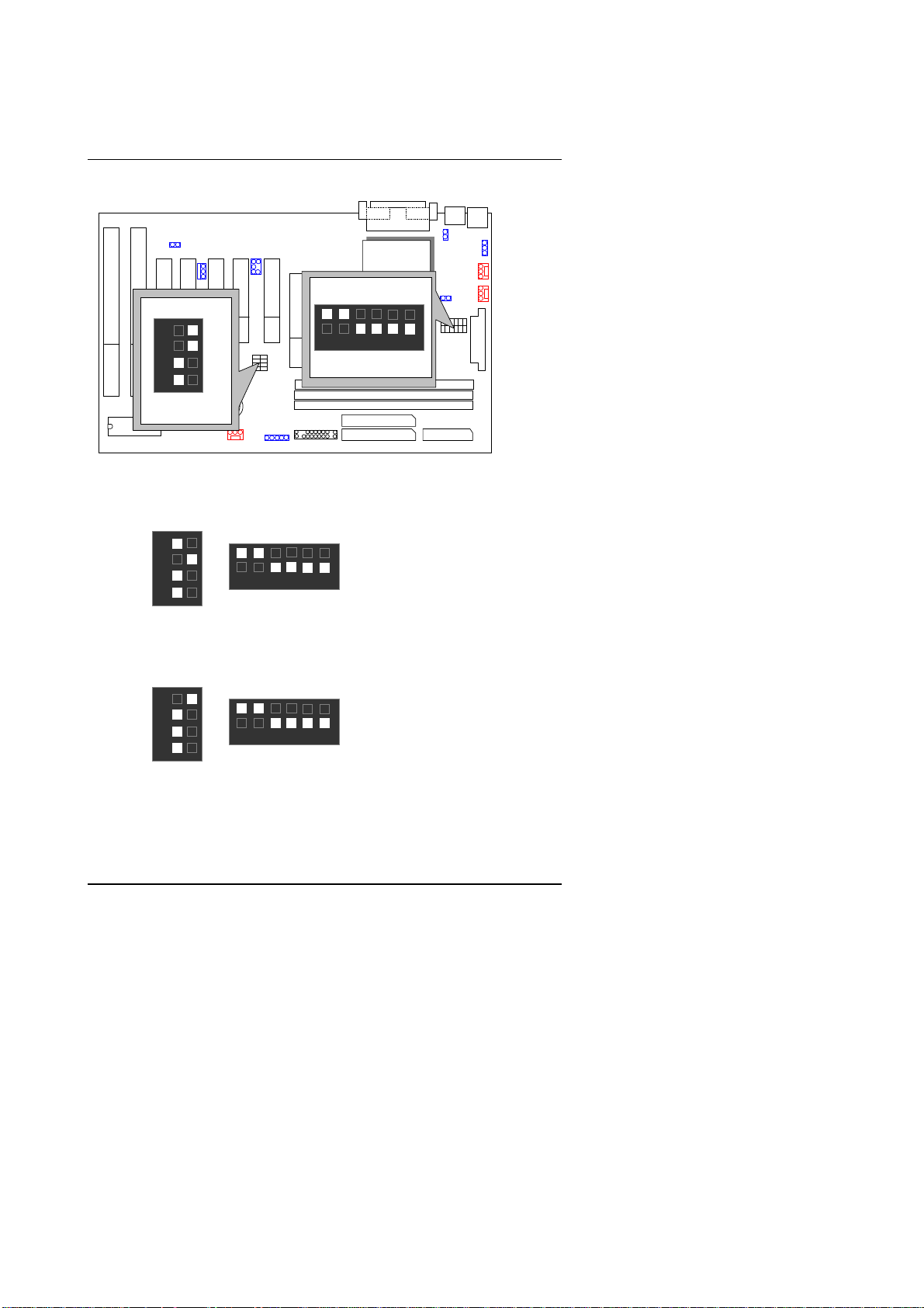
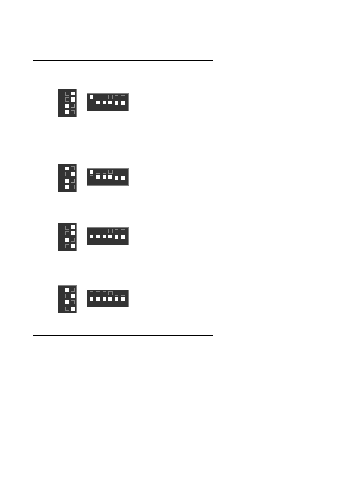
I. Quick Installation Guide :
The system bus speed can be set for 66,100,133MHz. The user can select the
system bus speed
(SW2)
and change the DIP SWITCH
up the CPU speed for 500MHz – 1GHz and faster processor.
The CPU speed must match with the frequency RATIO. It will cause
0000
system hanging up if the frequency RAT IO is higher than CPU's.
SW1: (O:ON / X:OFF)
(SW1)
selection to se t
FREQ. RATIO
1 2 3 4
X 3 O X O O
X 3.5 X X O O
X 4 O O X O
X 4.5 X O X O
X 5 O X X O
X 5.5 X X X O
X 6 O O O X
X 6.5 X O O X
X 7 O X O X
X 7.5 X X O X
X 8 O O X X
X 8.5 O X O O
X 9 X X O O
X 9.5 X O O O
X 10 X O X X
X 10.5 O O X O
X11 O X X X
X11.5 X O X O
X12 O X X O
X13 X X X O
X14 O O O X
X15 X O O X
X16 O X O X
DIP SWITCH
2
Page 5

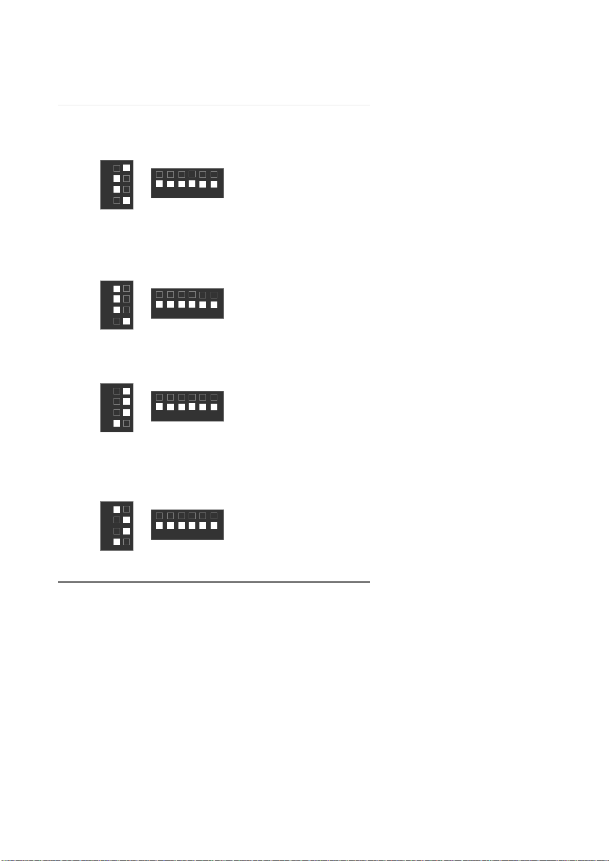
6VXE7+
Set System Bus Speed
SW2: (O:ON / X:OFF)
CPU PCICLK 1 2 3 4 5 6
66/100/
133/Auto
66 33.3
75 37.5
83 41.6
100 33.3
112 37.3
124 31
133 33.3
140 35
150 37.5
Note: We don’t recommend you to set up your system speed to
0000
0000
75,83,112,124,140 or 150MHz because these frequencies are not
the standard specifications for CPU, Chipset and most of the
peripherals. Whether your system can run under
75,83,112,124,140 or 150 MHz properly will depend on your
hardware configurations: CPU, SDRAM, Cards, etc.
Intel Processor all have locked Frequency Multiple, so you can not
change the CPU Frequency Multiple.
33.3
X X X X O O
O O X X X X
O O O X X X
O O X O X X
O X X X X X
O X O X X X
X X X O X X
X X X X X X
X X O O X X
X X O X X X
3
Page 6
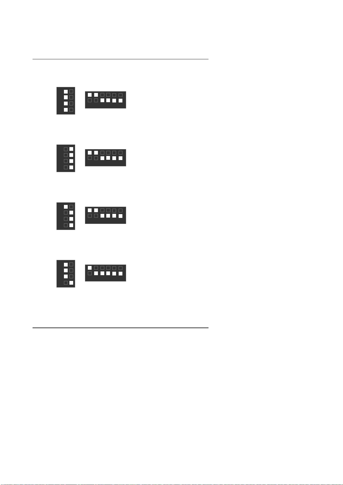
1. CeleronTM 533/ 66 MHz FS B
ON
1 2 3 4
PIIX4
6VXE7+
SW1
ON
82443BX
1 2 3 4 5 6
SW2
Quick Installation Guide
2. Celeron
TM
566/ 66 MHz FSB
ON
1 2 3 4
ON
1 2 3 4 5 6
SW1
3. CeleronTM 600/ 66 MHz FSB
ON
1 2 3 4
SW2
ON
1 2 3 4 5 6
SW1
SW2
4
Page 7
6VXE7+
4. CeleronTM 633/ 66 MHz FSB
1 2 3 4
ON
ON
1 2 3 4 5 6
SW1
5. CeleronTM 667/ 66 MHz FSB
ON
1 2 3 4
SW2
ON
1 2 3 4 5 6
SW1
6. CeleronTM 700/ 66 MHz FSB
ON
1 2 3 4
SW2
ON
1 2 3 4 5 6
SW1
7. Cyrix III 550/100MHz FSB
ON
1 2 3 4
SW2
ON
1 2 3 4 5 6
SW1
SW2
5
Page 8
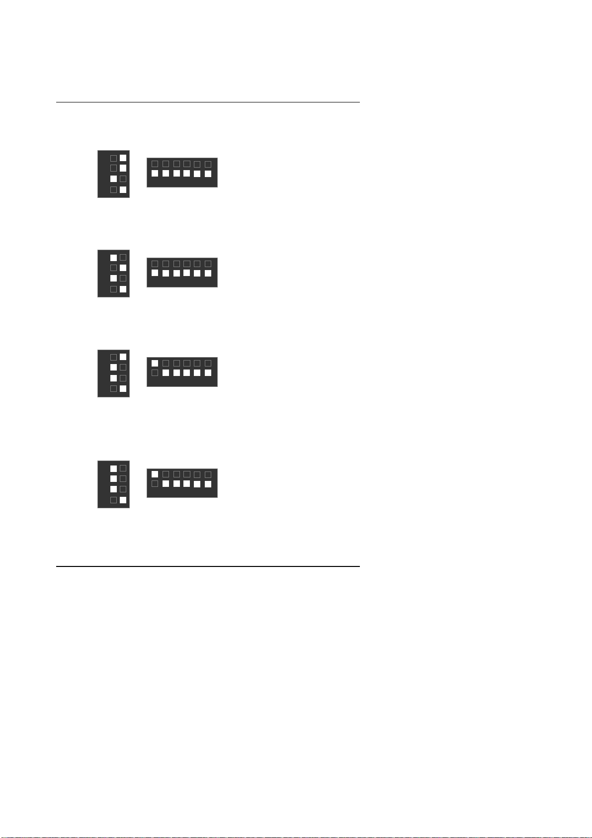
8. Cyrix III 533/133MHz FSB
1 2 3 4
ON
ON
1 2 3 4 5 6
Quick Installation Guide
SW1
9. Cyrix III 600/133MHz FSB
ON
1 2 3 4
SW2
ON
1 2 3 4 5 6
SW1
10. Pentium
1 2 3 4
®
500/100MHz FSB
!!!
ON
SW2
ON
1 2 3 4 5 6
SW1
11. Pentium
1 2 3 4
®
550/100MHz FSB
!!!
ON
SW2
ON
SW1
1 2 3 4 5 6
SW2
6
Page 9
6VXE7+
12. Pentium
1 2 3 4
®
600/100MHz FSB
!!!
ON
1 2 3 4 5 6
ON
SW1
13. Pentium
1 2 3 4
SW1
14. Pentium
1 2 3 4
SW1
15. Pentium
1 2 3 4
SW2
®
650/100MHz FSB
!!!
ON
ON
1 2 3 4 5 6
SW2
®
700/100MHz FSB
!!!
ON
ON
1 2 3 4 5 6
SW2
®
750/100MHz FSB
!!!
ON
ON
SW1
1 2 3 4 5 6
SW2
7
Page 10
16. Pentium
1 2 3 4
®
800/100MHz FSB
!!!
ON
ON
1 2 3 4 5 6
Quick Installation Guide
SW1
17. Pentium
1 2 3 4
SW1
18. Pentium
®
1 2 3 4
SW1
19. Pentium
®
1 2 3 4
SW2
®
850/100MHz FSB
!!!
ON
ON
1 2 3 4 5 6
SW2
533/133MHz FSB
!!!
ON
ON
1 2 3 4 5 6
SW2
600/133 MHz FSB
!!!
ON
ON
SW1
1 2 3 4 5 6
SW2
8
Page 11
6VXE7+
20. Pentium
1 2 3 4
®
667/133MHz FSB
!!!
ON
ON
1 2 3 4 5 6
SW1
21. Pentium
1 2 3 4
SW1
22. Pentium
1 2 3 4
SW1
23. Pentium
1 2 3 4
SW2
®
733/133MHz FSB
!!!
ON
ON
1 2 3 4 5 6
SW2
®
800/133MHz FSB
!!!
ON
ON
1 2 3 4 5 6
SW2
®
866/133MHz FSB
!!!
ON
ON
SW1
1 2 3 4 5 6
SW2
9
Page 12

24. Pentium
1 2 3 4
®
933/133MHz FSB
!!!
ON
ON
1 2 3 4 5 6
Quick Installation Guide
SW1
25. Pentium
1 2 3 4
SW1
SW2
®
1GHz /133MHz FSB
!!!
ON
ON
1 2 3 4 5 6
SW2
10
Page 13
6VXE7+
II. Jumper setting :
SPK : Speaker Connector
PIIX4
RST : Reset Switch
PIIX4
External Speaker
1
+
6VXE7+
PIN No. Function
Open Normal
Close Reset Hardware
6VXE7+
PIN No. Function
1 VCC
82443BX
2 NC
3 NC
4 Data
Operation
82443BX
System
11
Page 14
PW LED : Power LED Connector
Quick Installation Guide
−−−− −−−−
+
PIIX4
PIN No. Function
1 LED +
2
6VXE7+
3
HD : IDE Hard Disk Active LED
PIIX4
PIN No. Function
+
−−−−
6VXE7+
82443BX
LED −
LED −
82443BX
1 LED +
2
LED −
12
Page 15
6VXE7+
GN : Green Function Switch
PIIX4
GD : Green LED
PIIX4
PIN No. Function
82443BX
Open Normal Operation
Close Entering Green
6VXE7+
PIN No. Function
−−−−
Mode
82443BX
1 LED +
+
2
6VXE7+
LED −
13
Page 16
Soft POWER : Soft Power Connector
Quick Installation Guide
PIN No. Function
1 Signal
PIIX4
2 GND
6VXE7+
IR : Infrared Connector (Optional)
1
+
PIN No. Function
1 IR data output
2 GND
3 IR data input
PIIX4
4 NC
5 VCC(+5V)
6VXE7+
82443BX
82443BX
14
Page 17
6VXE7+
ATX POWER : ATX Power Connector
Pin No. Function
3,5,7,13,
GND
15-17
1,2,11 3.3V
4,6,19,20 VCC
10 +12V
12 -12V
PIIX4
18 -5V
8 Power Good
6VXE7+
9 5V SB stand by+5V
14 PS-ON(Soft On/Off)
PS/2 Mouse / Keyboard Connector
PS/2 Mouse
5 6
PIIX4
4
PS/2 Keyboard
6VXE7+
3
1 2
10 20
82443BX
1 11
PS/2 Mouse/ Keyboard
Pin No. Function
1 Data
2 NC
3 GND
82443BX
4 VCC(+5V)
5 Clock
6 NC
15
Page 18
J2: CPU FAN
J3: PW R FAN
PIIX4
1
6VXE7+
Quick Installation Guide
PIN No. Function
1 GND
2 +12V
3 SENSE
82443BX
PIN No. Function
1 GND
2 +12V
1
PIIX4
6VXE7+
3 SENSE
82443BX
16
Page 19
6VXE7+
J15 :SYSTEM FAN
PIN No. Function
1
PIIX4
1 GND
2 +12V
3 SENSE
6VXE7+
IDE1: For Primary IDE Port
PIIX4
6VXE7+
82443BX
82443BX
1
17
Page 20
IDE2: For Secondary IDE Port
PIIX4
6VXE7+
FLOPPY : Floppy Port
Quick Installation Guide
82443BX
1
82443BX
PIIX4
6VXE7+
1
18
Page 21
6VXE7+
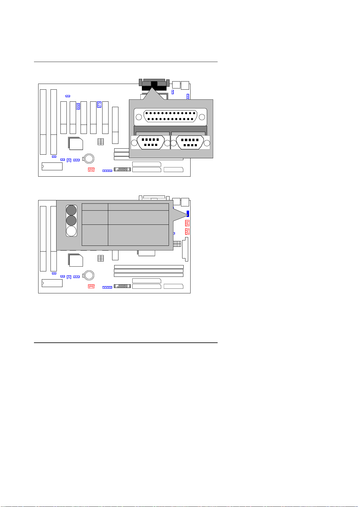
LPT PORT / COM A / COM B
PIIX4
6VXE7+
JP1 : PS/2 Keyboard Power On Selection
3
2
1
PIN No. Function
1-2
close
2-3
close
PS/2 Keyboard
Power on Enabled
PS/2 Keyboard
Power on Disabled
COM B
(Default)
PIIX4
6VXE7+
LPT PORT
82443BX
COM A
82443BX
19
Page 22
Quick Installation Guide
USB : USB Port
PIIX4
JP7: Wake On LAN
5
1
6
2
3
6VXE7+
8 7
PIN No. Function
1
2 USB D0-
3
4 GND
5
6 USB D1-
4
7 USB D1+
8 GND
USB V0
USB D0+
USB V1
82443BX
1
2
3
PIN No. Function
1 +5V SB
PIIX4
2 GND
3 Signal
6VXE7+
82443BX
20
Page 23
6VXE7+
JP9 : Clear CMOS Function
PIN No. Function
1-2 close Clear CMOS
2-3 close Normal (Default)
J14 :SB-LINK
3 2 1
PIIX4
PIIX4
6VXE7+
6VXE7+
82443BX
6
4
2
PIN No. Function
5
3
1
1 Signal
2 GND
3 NC
4 Signal
5 GND
82443BX
6 Signal
21
Page 24
J16: Internal Modem Ring On
1
PIN No. Function
1 Signal
2 GND
PIIX4
6VXE7+
JP10 : Case Open (Optional)
Quick Installation Guide
82443BX
1
PIN No. Function
1 Signal
2 GND
PIIX4
6VXE7+
82443BX
22
Page 25
6VXE7+
JP15 : O v er Volt age
(When JP15 set ”Open”, CPU Voltage is rising 10%)
(Magic Booster)
1
PIN No. Function
(Optional)
open Turbo
short Normal
82443BX
(Default)
PIIX4
6VXE7+
JP16 : BIOS Flash ROM Write Protection
1
PIN No. Function
open Normal (Default)
short Write Protection
Please Set Jumper JP16 to “Open” to
0000
enabled BIOS Write Function When
you update new BIOS or new device.
PIIX4
6VXE7+
82443BX
23
Page 26
J17 : Cyrix CPU Turbo Function (Optional)
1
PIN No. Function
open Normal
short Turbo
82443BX
PIIX4
6VXE7+
JP17 : System After AC Back
Quick Installation Guide
PIN No. Function
1
open Soft Off
PIIX4
short Full On
6VXE7+
82443BX
24
Page 27

6VXE7+
BAT1 :Battery
PIIX4
Danger of explosion if battery is
0
incorrectly replaced.
Replace only with the same or
0
equivalent type recommended by the
manufacturer.
Dispose of used batteries according
0
to the manufacturer’s instructions.
6VXE7+
+
82443BX
25
Page 28

Quick Installation Guide
III. Top Performance Test Setting:
Users have to modify the value for each item in chi pset features as follow
for top performance setting.
**
Each value of items as above depends on your hardware configuration :
CPU , SDRAM , Cards , etc.
Please modify each value of items If your system does not work properly .
26
Page 29

6VXE7+
The following performance data list is the testing results of some popular
benchmark testing programs.
These data are j ust ref erred by user s, and th ere is no respon si bili ty for di ffer ent
testing data values gotten by users. (Different Hardware & Software
configuration will result in different benchmark testing results.)
•
CPU Intel Socket 370 Processor
•
DRAM (128 x 1) MB SAMSUNG (SECKM48S803CT-GA)
•
CACHE SIZE 128 KB included in CPU (Celeron);
256 KB included in CPU (Pentium
•
DISPLAY GA-660 AGP Card (32M B SDRAM)
•
STORAGE Onboard IDE (IBM DJNA-371800) (18GB)
•
O.S. Windows NT™ 4.0 (SP6a)
•
DRIVER Displa y Driver at 1024 x 768 x 64K x 75Hz
Intel Celeron
Socket 370
Processor
Winbench99
CPU mark99
FPU Winmark 99
Business Disk Winmark 99
Hi-End Disk Winmark 99
Business Graphics Winmark 99
Hi-End Graphics Winmark 99
Winstone99
400MHz
(100x4)
33.8 38.4 62.1 55.8
2140 2860 3760 3210
4950 4670 5550 5140
13000 12300 12700 13200
181 188 312 298
352 400 626 572
533MHz
(66x8)
TM
®
!!!)
Intel Pentium
Socket 370
700MHz
(100x7)
600MHz
(133x4.5)
®
!!!
Business Winstone99 29.7 30.7 40.5 39.5
Hi-End Winstone99 27.4 30.1 39.9 38.4
27
Page 30

Page 31

TABLE OF CONTENTS
Table of Contents
1. INTRODUCTION
1.1. PREFACE ................................................................................................ 1-1
1.2. KEY FEATHERS...................................................................................... 1-1
1.3. PERFORMANCE LIST............................................................................. 1-2
1.4. BLOCK DIAGRAM.................................................................................... 1-3
1.5. INTRODUCE THE INTELCeleron
1.6. WHAT IS AGP?........................................................................................ 1-4
TM
Socket 370 Processor................... 1-4
2. SPECIFICATION
2.1. HARDWARE ............................................................................................ 2-1
2.2. SOFTWARE............................................................................................. 2-2
2.3. ENVIRONMENT....................................................................................... 2-2
3. HARDWARE INSTALLATION
3.1. UNPACKING............................................................................................ 3-1
3.2. MOTHERBOARD LAYOUT...................................................................... 3-2
3.3. QUICK REFERENCE FOR JUMPERS & CONNECTORS.... .. .. .. .. ... .. .. ..... 3-2
3.4. DRAM INSTALLATION............................................................................. 3-6
3.5. CPU SPEED SETUP.. .. .. ............... .. .. ... .. .. .. .. .. ............... .. .. ... .. .. .. .. .. .. ........ 3-6
3.6. CMOS RTC & ISA CFG CMOS RAM................. .. .. .. .. ............................... 3-7
3.7. SPEAKER CONNECTOR INSTALLATION............................................... 3-8
3.8. HARDWARE RESET SWITCH CONNECTOR INSTALLATION .......... .. ... 3-8
3.9. POWER LED CONNECTOR INSTALLATION .......................................... 3-8
3.10. IDE & ATAPI DEVICE INSTALLATION.......... .. ... .. .. .. .. .. ... ................ ... .. .. 3-8
1
Page 32

6VXE7+
3.11. PERIPHERAL DEVICE INSTALLATION................................................. 3-8
3.12. KEYBOARD & PS/2 MOUSE INSTALLATION........................................ 3-8
4. BIOS CONFIGURATION
4.1. ENTERING SETUP.................................................................................. 4-1
4.2. CONTROL KEYS ..................................................................................... 4-2
4.3. GETTING HELP....................................................................................... 4-3
4.3.1. Main Menu .......... .. ... .. .. .. .. .. ... .. .. ................................ ................ 4-3
4.3.2. Status Page Setup Menu / Option Page Setup Menu..................... 4-3
4.4. THE MAIN MENU..................................................................................... 4-3
4.5. STANDARD CMOS SETUP MENU.......................................................... 4-5
4.6. BIOS FEATURES SETUP........................................................................ 4-9
4.7. CHIPSET FEATURES SETUP ................................................................. 4-13
4.8. POWER MANAGEMENT SETUP........ .. .. ... .. ............... .. .. .. .. .. .. ... .. .. .. .. ...... 4-15
4.9. PNP/PCI CONFIGURATION ................................................................... 4-19
4.10. LOAD BIOS DEFAULTS............... ............... .. .. .. .. .. .. .. ... .. .. .. .. .. ............... . 4-21
4.11. LOAD PERFORMANCE DEFAULTS...................................................... 4-22
4.12. INTEGRATED PERIPHERALS............................................................... 4-23
4.13.SUPERVISOR/USER PASSWORD......................................................... 4-26
4.14. IDE HDD AUTO DETECTION .......... .. ... ............... .... .. .. .. .. .. ... .. .. .. ........... 4-27
4.15. SAVE & EXIT SETUP...... .. .. .. ... .. ................. .. .. .. .. .. ... .. .. .. ............... .. .. .. .. . 4-28
4.16. EXIT WITHOUT SAVING....................................................................... 4-29
APPENDIX
……………………………………………………………………………….A-1
2
Page 33

Introduction
1. INTRODUCTION
1.1. PREFACE
Welcome to use the
/Pentium
®
)and Cyrix III Socket 370 Processor based PC / AT Compatible
!!!
6VXE7+
motherboard. It is a Intel
(Celeron
TM
®
system with AG P / PCI / ISA B us, and ha s been desi gned to be th e fas test PC /
AT system. There are some ne w features allow you to operate the system with
just the performance you want.
This manual also explains how to install the motherboard for operation, and
how to set up your CMOS CONFIGURATION with BIOS SETUP program.
1.2. KEY FEATURES
Socket 370 Processor based PC / AT compatible main board.
Socket 370 Pins ZIF white socket on board.
Supports Socket 370 processor running at 500MHz-1GHz and faster .
Intel Pentium !!! 100/133MHz FSB, FC-PGA
Intel CeleronTM 66MHz FSB, PPGA/FC-PGA
VIA Cyrix III 100/133MHz FSB, PPGA
PCB Ver.3.0 No Suppor t Intel PPGA Processor
0000
VIA Apollo chipset, Supports AGP / SDRAM / Ultra DMA 33 / ATA 66
IDE / Keyboard and PS/2 Mouse Power On / ACPI features.
Supports 3xDIMMs using 3.3V EDO or SDRAM DIMM module.
Supports ext ernal Modem Ring-On on COMA & COMB a nd internal Modem
Ring-On.
Supports EDO 16MB ~ 384 MB, SDRAM 16MB ~ 1.5GB (256Mb DRAM
technology) me mory on board.
Supports Wake-up on LAN .
Supports ECC or Non-ECC type DRAM module.
1xAGP slot, 5xPCI Bus slots, 2xISA Bus slots.
Supports 2 channels Ultra DMA33/ATA66 IDE ports for 4 IDE Devices.
Supports 2xCOM (16550), 1xLPT (EPP / ECP), 1x Floppy port.
Supports 2xUSB port & PS/2 Mouse/ Keyboard port.
Licensed AWARD BIOS, 2M bits FLASH ROM.
30.5cm x 19 cm ATX SIZE form factor, 4 layers PCB.
1-1
Page 34

6VXE7+
1.3. PERFORMANCE LIST
The following performance data list is the testing results of some popular
benchmark testing programs.
These data are just referred by users, and there is no responsibility for different
testing data values gotten by users. (Different Hardware & Software
configuration will result in different benchmark testing results.)
•
CPU Intel Socket 370 Processor
•
DRAM (128 x 1) MB SAMSUNG (SECKM48S803CT-GA)
•
CACHE SIZE 128 KB included in CPU (Celeron);
256 KB included in CPU (Pentium
•
DISPLAY GA-660 AGP Card (32M B SDRAM)
•
STORAGE Onboard IDE (IBM DJNA-371800) (18GB)
•
O.S. Windows NT™ 4.0 (SP6a)
•
DRIVER Displa y Driver at 1024 x 768 x 64K x 75Hz
Intel Celeron
Socket 370
Processor
Winbench99
CPU mark99
FPU Winmark 99
Business Disk Winmark 99
Hi-End Disk Winmark 99
Business Graphics Winmark 99
Hi-End Graphics Winmark 99
Winstone99
400MHz
(100x4)
33.8 38.4 62.1 55.8
2140 2860 3760 3210
4950 4670 5550 5140
13000 12300 12700 13200
181 188 312 298
352 400 626 572
533MHz
(66x8)
Business Winstone99 29.7 30.7 40.5 39.5
Hi-End Winstone99 27.4 30.1 39.9 38.4
TM
®
)
!!!
Intel Pentium
Socket 370
700MHz
(100x7)
600MHz
(133x4.5)
®
!!!
1-2
Page 35

Introduction
66 /100 /133 MHz
66 /100 /133 MHz
66 /100 /133 MHz
1.4. BLOCK DIAGRAM
PGA 370
AGP
Ultra
DMA33/
ATA66
IDE Ports
AGP Bus
66MHz
IDE Bus
82C693A
PCI Bus
82C596B
VIA
VIA
Host Bus
33MHz
33 MHz
33 MHz
48MHz
14.318MHz
14.318MHz
Clock
Generator
3.3V SDRAM
DIMM Sockets
24MHz
USB Ports
ISA Bus
USB Bus
14.318MHz
1-3
I/O
CHIPSET
ITE8671
COM Ports
LPT Port
Floppy Port
Keyboard
PS/2 Mouse
Page 36

6VXE7+
1.5. INTRODUCE THE INTEL
Figure 1: INTEL Pentium
Figure 2: INTEL Pentium
1.6 What is AGP
????
Pentium
Socket 370 Processor
!!!
Socket 370 Processor(FC-PGA)
!!!
Socket 370 Processor(PPGA)
!!!
The Accelerat ed Graphics Po rt (AGP) is a new port on the Host-To-PCI brid ge
device that supp orts an AGP port. The main purpose of th e AGP port is to
provide fast access to system memory.
The AGP port can be used either a s fast PCI port ( 32-bits at 66MHz vs.32-Bits
at 33MHz) or as an AGP port which supports 2x data-rate, a read queue, and
side band addressi ng. When the 2x -data rate is use d the port can tr ansmit data
at 533MB/sec (66.6*2*4). The read-queue can be used to pipeline reads –
removing the effects of the reads-l atency. Side band addressing can be used
to transmit the data address on a separate line in order to speed up the
transaction.
1-4
Page 37

2. SPECIFICATION
2.1. HARDWARE
Specification
CPU
•
• CHIPSET
•
SPEED
•
DRAM MEMORY
• CACHE
MEMORY
• I/O BUS SLOTS
−
Support Socket 370 Processor:
−
370 pins 66/100/133MHz socket on board.
Intel Pentium
Intel CeleronTM 66MHz FSB, PPGA/FC-PGA
VIA Cyrix III 100/133MHz FSB, PPGA
PCB Ver.3.0 No Suppor t Intel PPGA Processor
0000
−
VT82C693A PCI/AGP Controller(PAC)
−
VT82C596B PCI ISA IDE Controller.
−
66/100/133MHz system speed.
−
66 MHz AGP bus speed. (2X mode 133MHz)
−
33 MHz PCI-Bus speed.
−
8 MHz AT bus speed.
−
3 banks 168 pins DIMM module sockets on board.
−
Use 16 / 32 / 64 / 128 / 256 / 512MB DIMM module
!!! 100/133MHz FSB, FC-PGA
500MHz– 1GHz and faster.
DRAM.(256Mb DRAM technology)
−
Supports EDO 16MB ~ 384 MB,
SDRAM 16MB~1.5GB.
(256Mb DRAM technology)
−
Supports 3.3V EDO / SDRAM.
−
Supports ECC or Non-ECC type DRAM.
−
32 KB L1 cache memory i ncluded in CPU.
−
128/256 KB L2 cache memory (included in CPU).
−
Supports DIB speed mode for L2 Cache.
−
5 33MHz Master / Slave PCI-BUS.
−
2 8MHz 16 bits ISA BUS.
−
1 66MHz / 133MHz AGP bus.
•
IDE PORTS
−
2 Ultra DMA 33/ATA66 Bus Master IDE channels
onboard. (Using IRQ14,15)
2-1
Page 38

6VXE7+
•
I/O PORTS
•
GREEN
FUNCTION
•
BIOS
• DIMENSION
2.2. SOFTWARE
−
Support Mode 3,4 IDE & ATAPI CD – ROM.
−
Supports 2 16550 COM ports.
−
Supports 1 EPP/ECP LPT port.
−
Supports 1 Floppy port.
−
Supports 2 USB ports.
−
Supports PS/2 Mouse & PS/2 Keyboard.
−
Suspend mode support.
−
Green switch & Green LED support.
−
IDE & Display power down support.
−
Monitor all IRQ / DMA / Display / I/O events.
−
2M bits FLASH ROM.
−
Supports Plug & Play, DMI Function.
−
ATX Form Factor, 4 layers PCB.
•
DRIVER
•
BIOS
•
O.S.
2.3. ENVIRONMENT
•
Ambient Temp.
•
Relative Hum.
•
Altitude
•
Vibration
•
Electricity
−
TUCD (Bus Ma ster + U tilities )
−
Licensed AWARD BIOS.
−
AT CMOS Setup, BIOS / Chipset Setup, Green
Setup, Hard Disk Utility included.
−
Operation with MS-DOS, Windows95,
98,
Windows
Windows NT™, OS/2, NOVELL and
SCO UNIX.
−
0°C to +50°C (Operating).
−
0 to +85% (Operating).
−
0 to 10,000 feet (Operating).
−
0 to 1,000 Hz.
−
4.9 V to 5.2 V. (Max. 20A current at 5V.)
2-2
Page 39

3. HARDWARE INSTALLATION
3.1. UNPACKING
The Motherboard package should cont ain the following:
Hardware Installation
•
•
•
•
The motherboard contains sensitive electric components, which can be easily
damaged by static electricity, so the Motherboard should be left in its original
packing until it is installed.
Unpacking and installation should be done on a grounded anti-static mat. The
operator should be wearing an anti sta tic wristb and, groun ded at th e same poi nt
as the anti-static mat.
Inspect the Motherboard carton for obvious damage. Shipping and handling
may cause damage to your board. Be sur e there are no shipping and handling
damages on the board before proceeding.
After opening the Motherboard carton, extract the system board and place it
only on a grounded anti-static surface component side up. Again inspect the
board for damage. Press down on all of the socket IC's to make sure that they
are properly seated. Do thi s only on with the bo ard placed on a firm flat surfa ce.
0000
6VXE7+
The
USER’S MANUAL for Motherboard.
Cable set for IDE, Floppy devices.
A CD for Motherboard Utili ty.(TUCD)
DO NOT APPLY POWER TO THE BOARD IF IT HAS BEEN DAMAGED.
Motherboard.
3-1
Page 40

6VXE7+
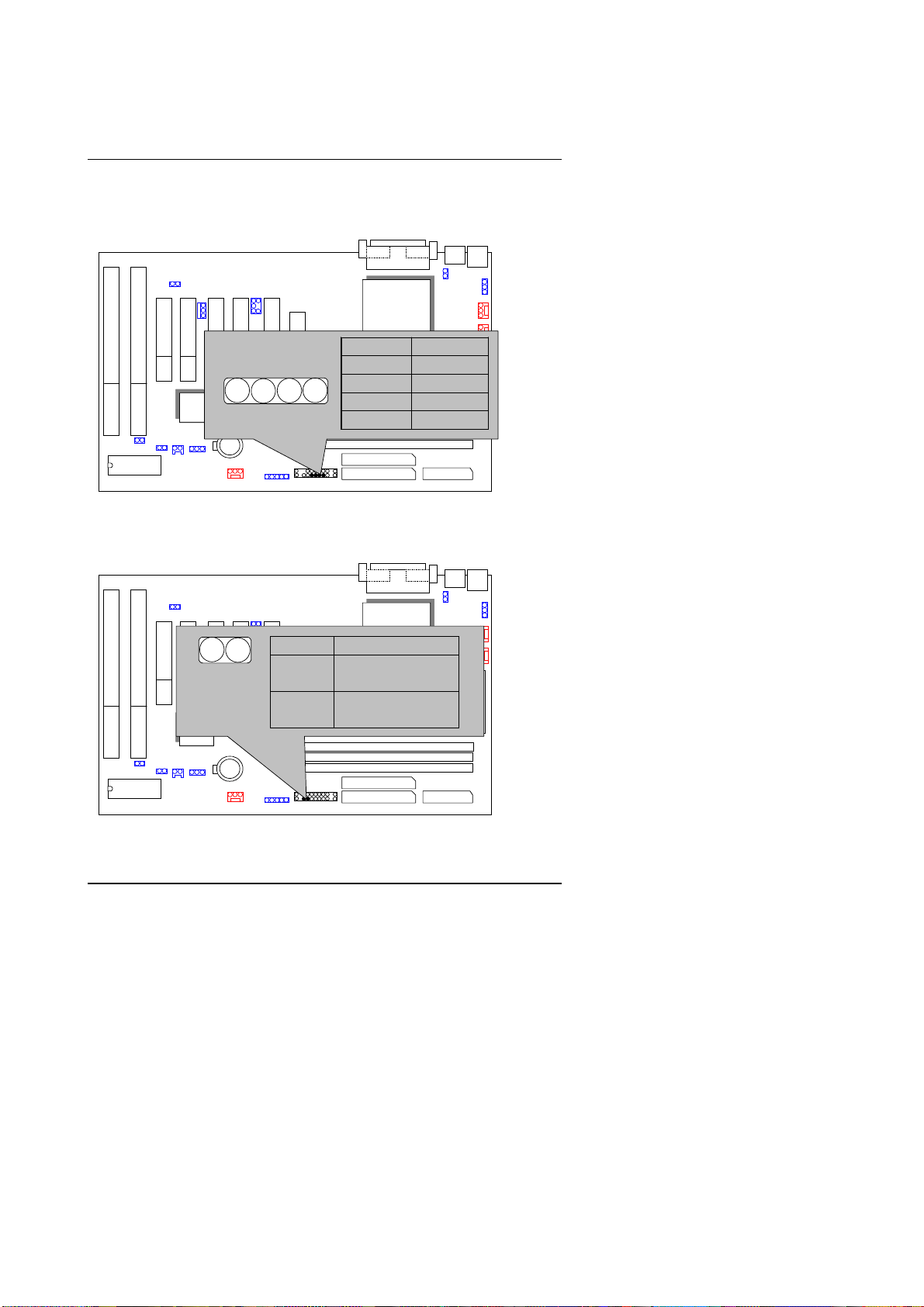
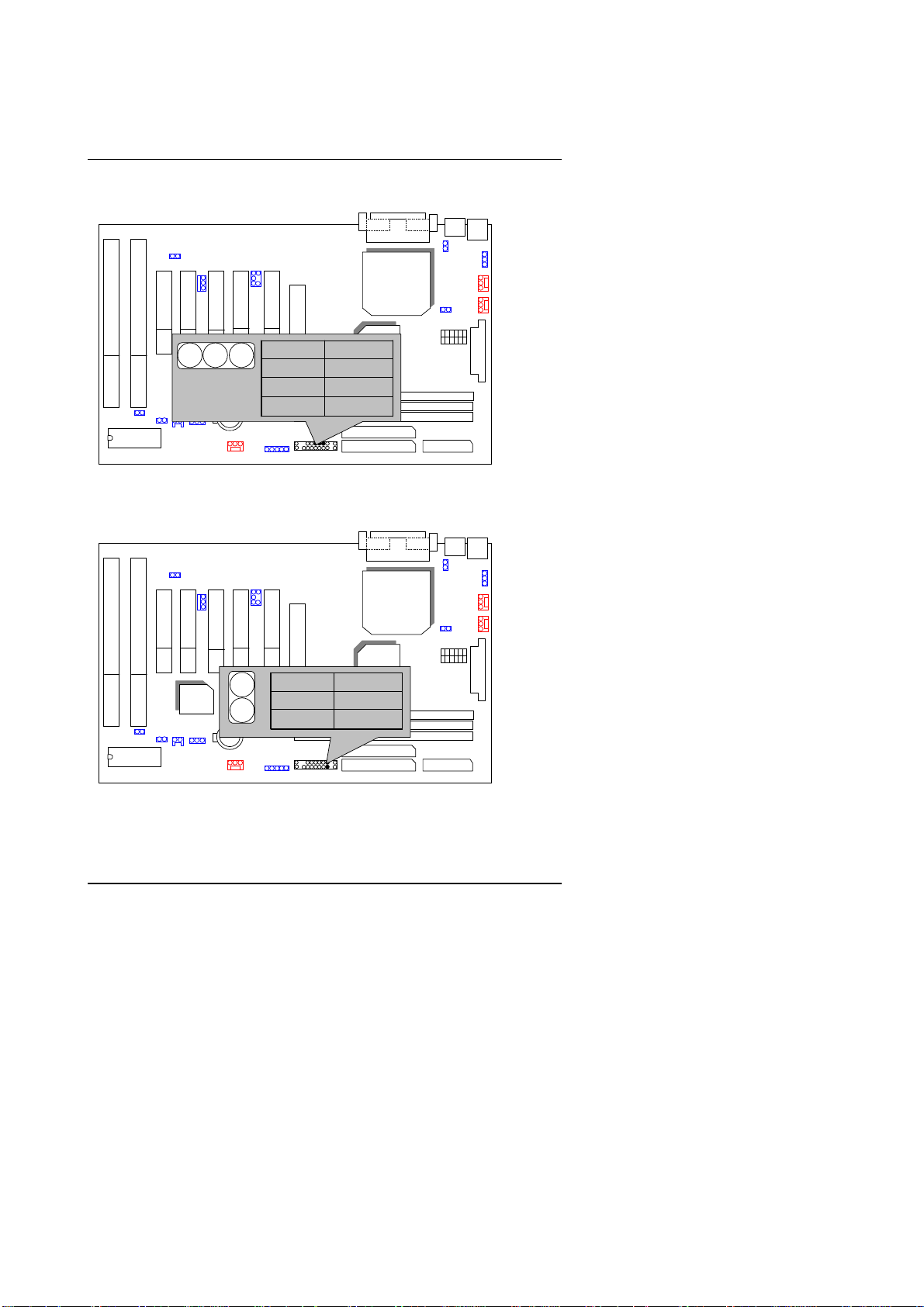
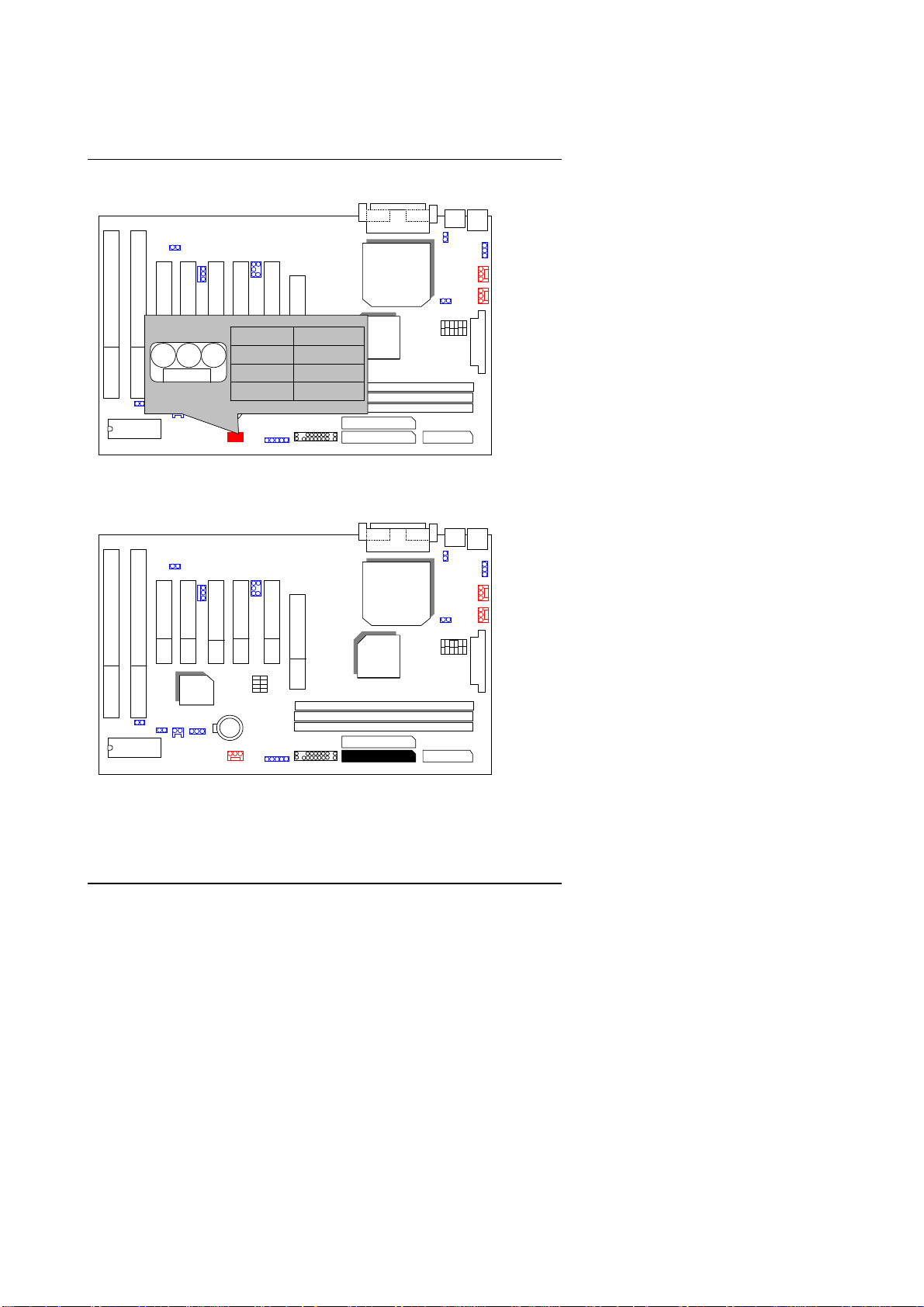
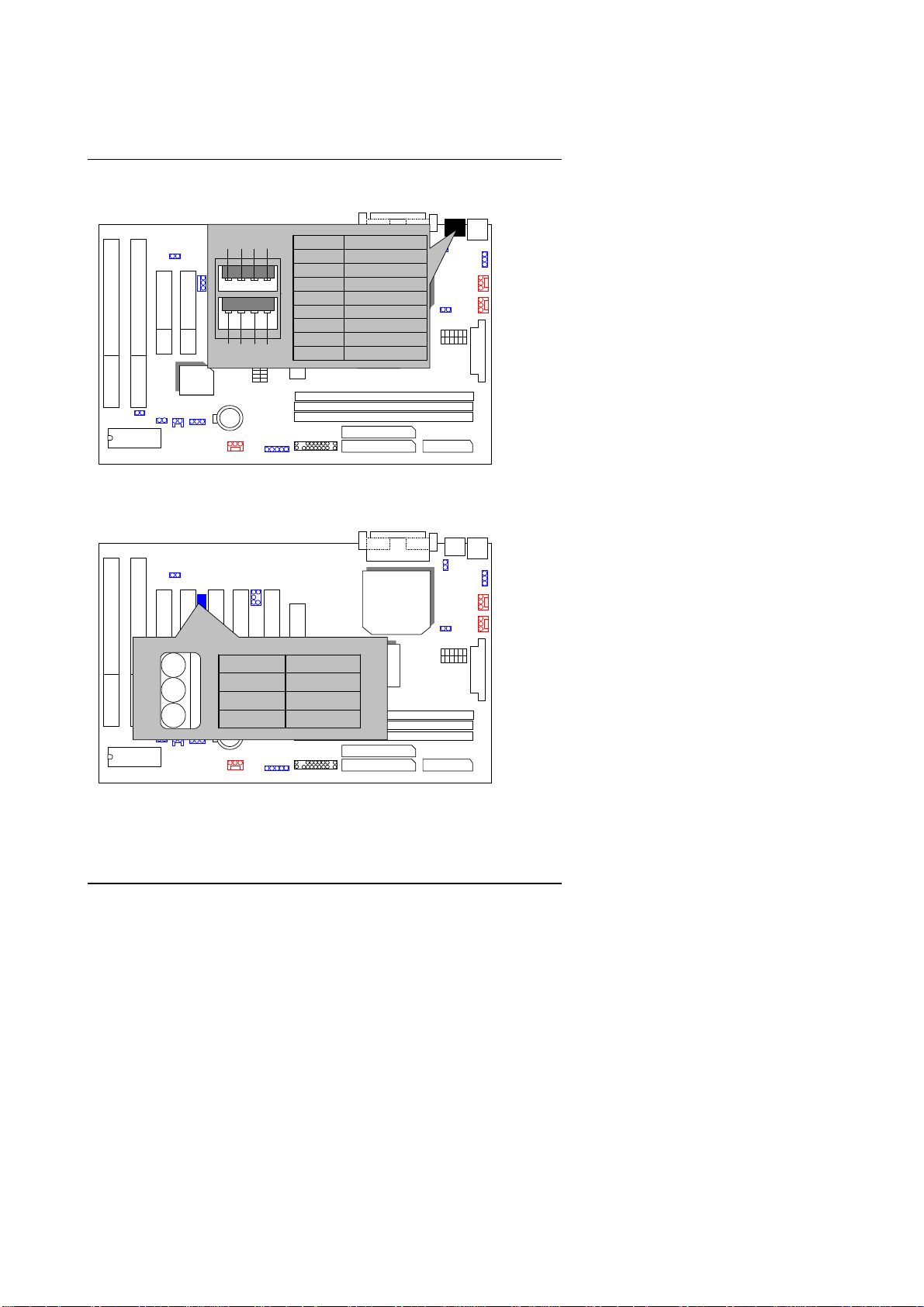
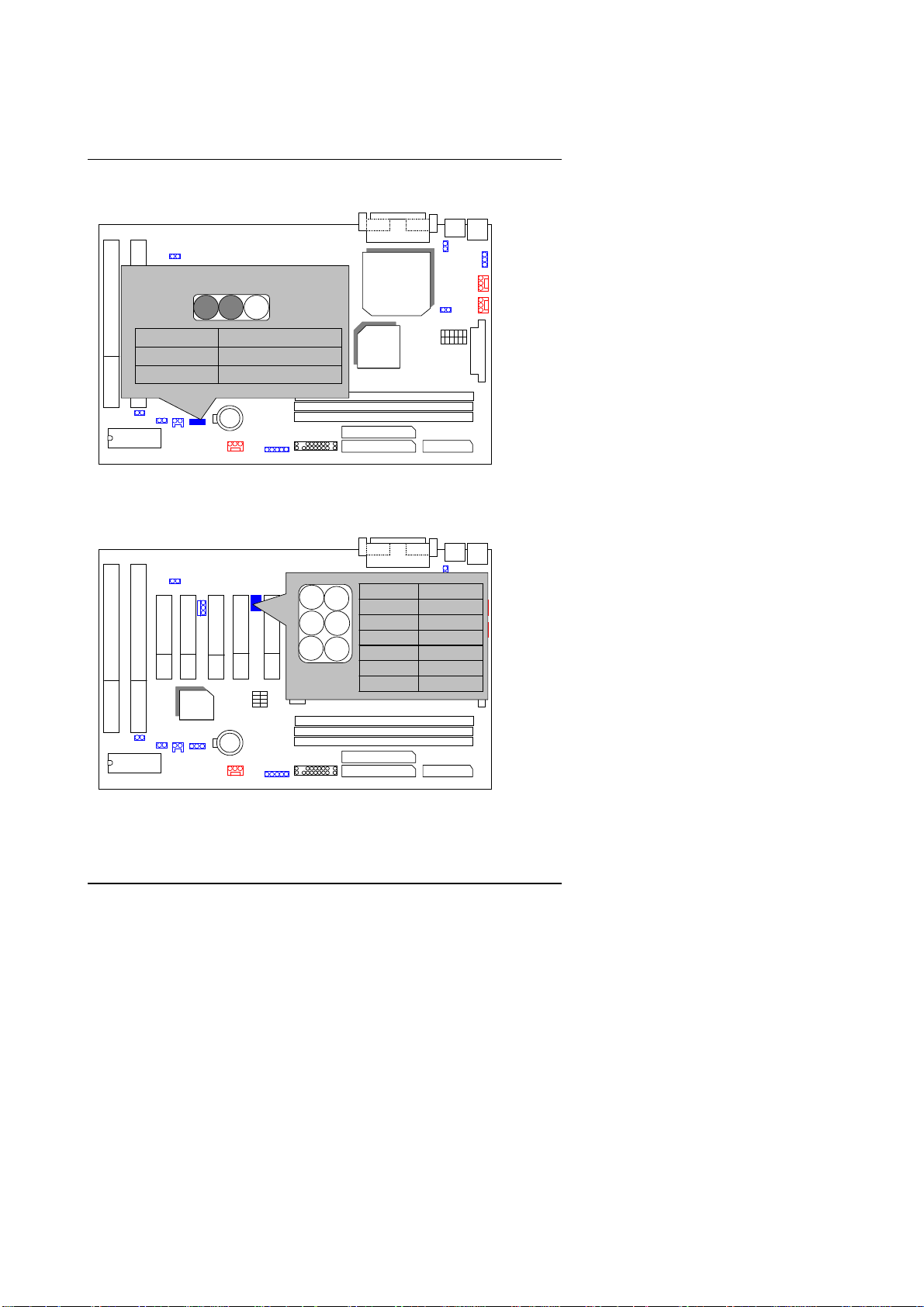
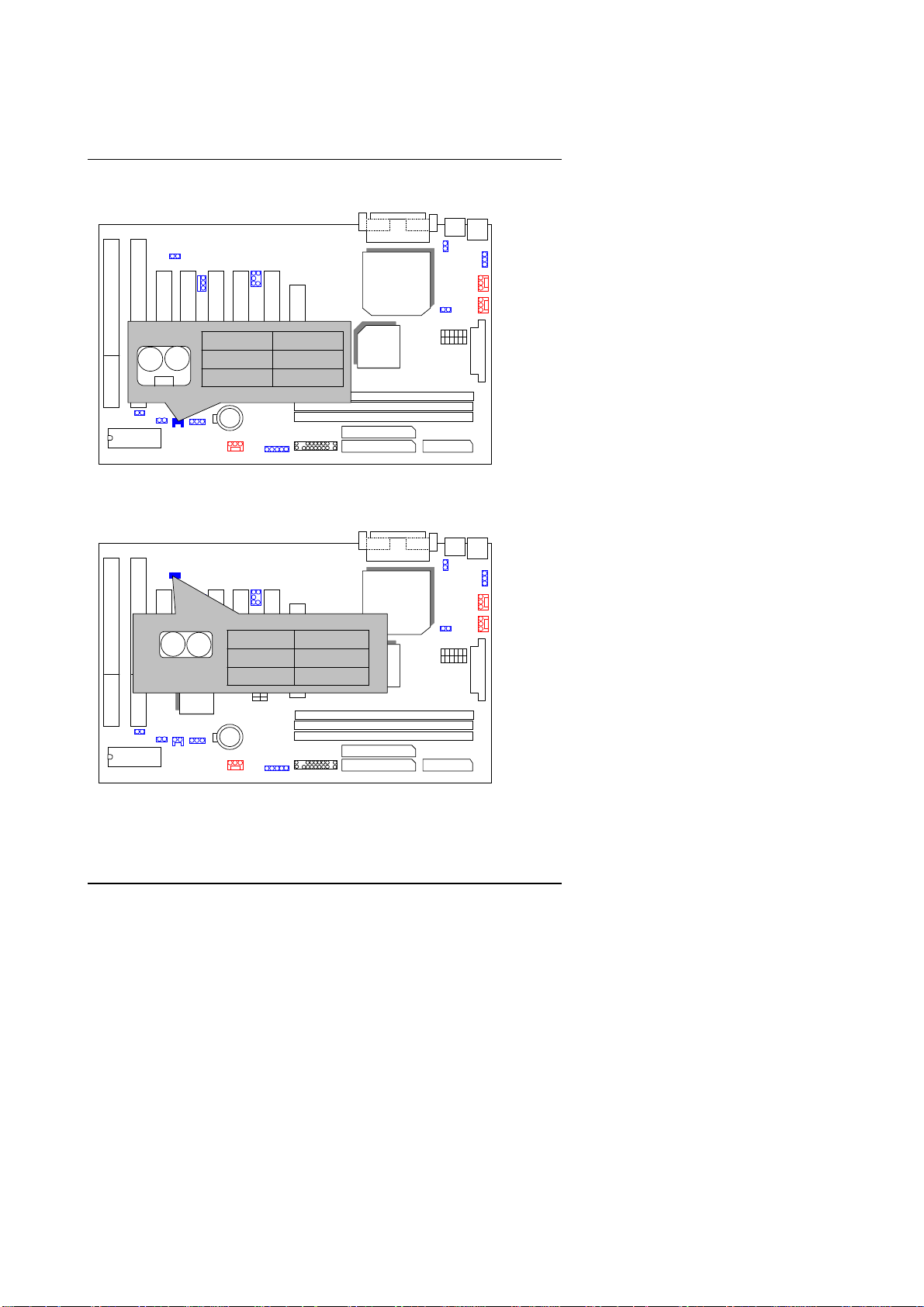
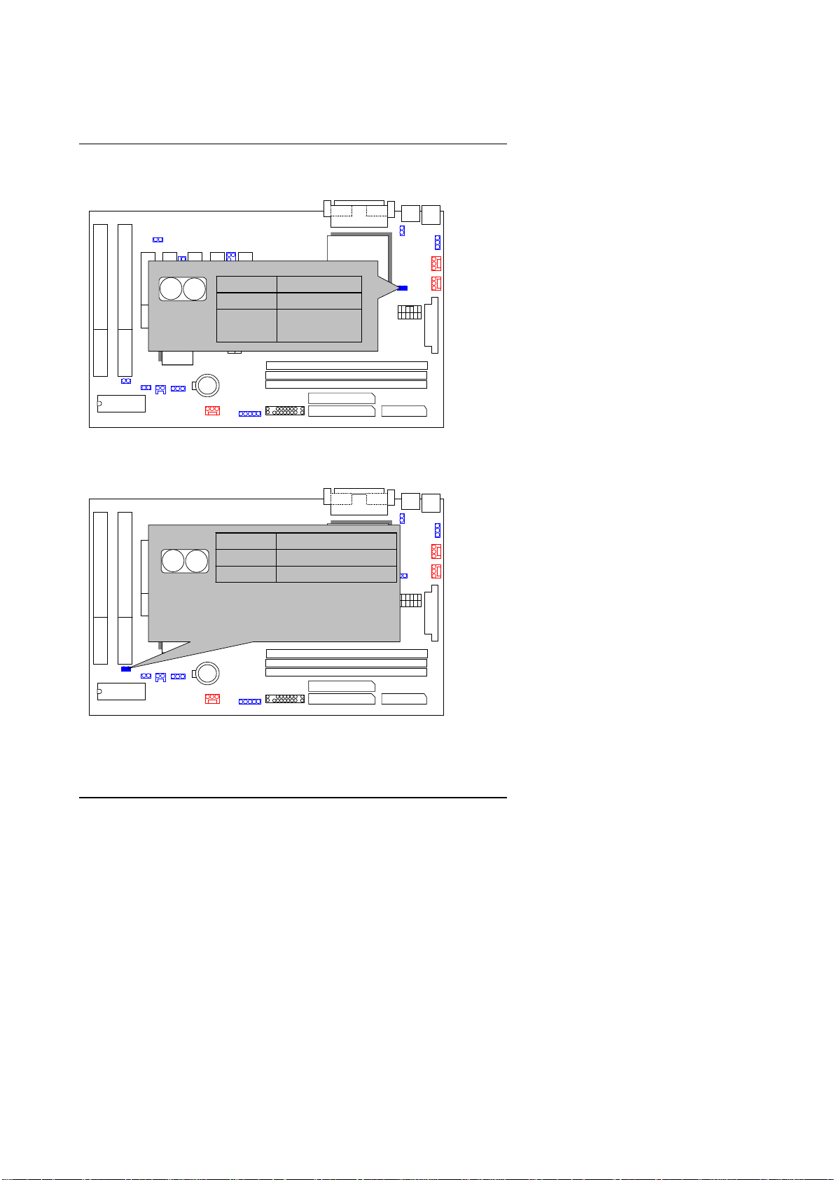
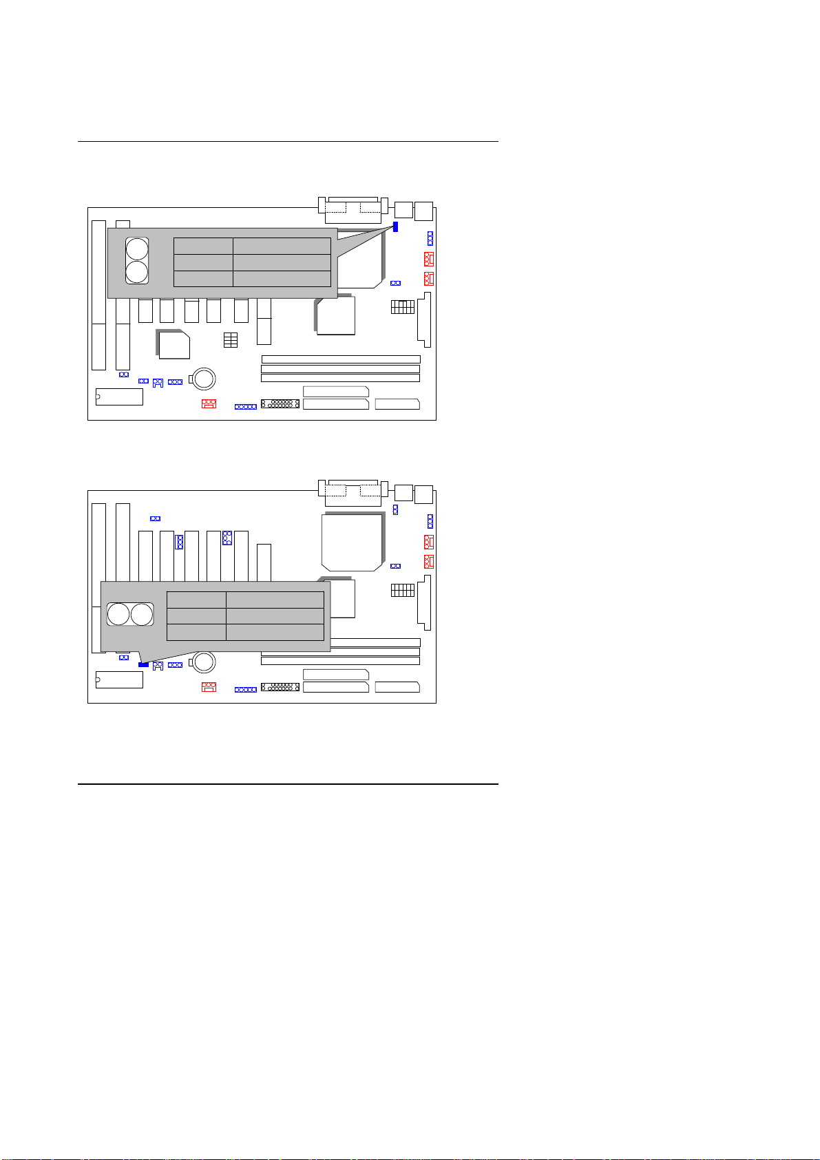
3.2. MOTHERBOARD LAYOUT
COM B
IDE 2
IDE 1
COM A
VT82C
82443BX
693A
LPT
CPU
ISA 2
JP16
BIOS
JP10
JP7
PCI 4
PCI 5
ISA 1
VT82C
PIIX4
596B
J16
JP17
JP9
J14
PCI 1
PCI 2
PCI 3
6VXE7+
BAT
J15
AGP
SW1
BANK 0
BANK 1
BANK 2
IR
½
Figure 3.1¾
JP4
JP15
Floppy
USB
SW2
PS/2
J17
JP1
J2
J3
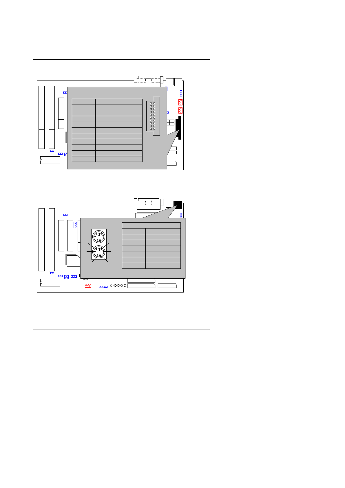
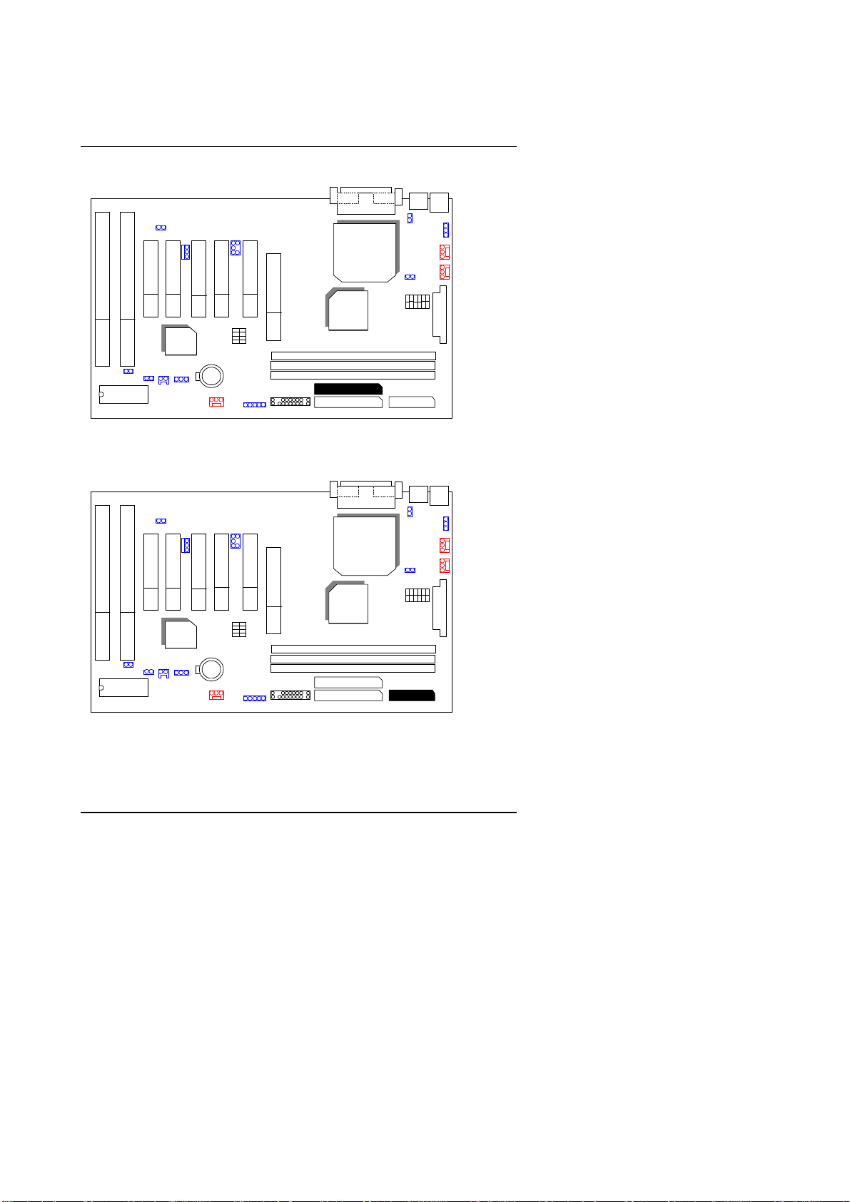
3.3. QUICK REFERENCE FOR JUMPERS & CONNECTOR S
I/O Ports Connector
USB USB port.
PS/2 For PS/2 Keyboard and Mouse port.
IDE 1/ IDE 2 For Primary / Secondary IDE port.
Floppy For Floppy port.
COM B For Serial port2 (COM B).
COM A For Serial port1 (COM A).
LPT For LPT port.
ATX Power For ATX Power Connector.
Socket 370
For CeleronTM , Pentium
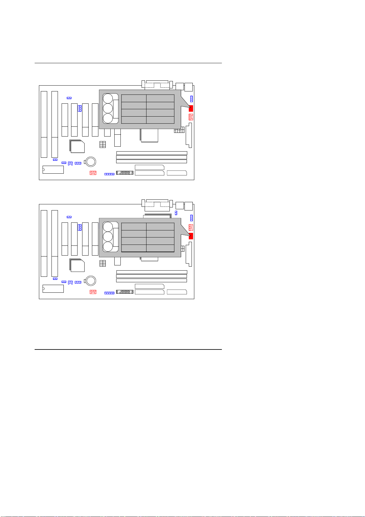
J2: CPU FAN
Pin No. Function
1 GND.
2 +12V.
3 Sense.
®
, Cyrix III Socket 370 processor inst alled
!!!
ATX POWER
3-2
Page 41

J3: PWR FAN
Pin No. Function
1 GND.
2 +12V.
3 Sense.
J15: System FAN
Pin No. Function
1 GND.
2 +12V.
3 Sense.
JP1: PS/2 Keyboard Power On Selection
Pin No. Function
1-2 short Enable PS/2 Keyboard power on.
2-3 short Disable PS/2 Keyboard power on.(Default)
JP7: WAKE ON LAN ( Wake on LAN Connector)
Pin No. Function
1 +5VSB.
2 GND.
3 Signal.
J16: RING PWR ON ( Internal Modem Ring On)
Pin No. Function
1 Signal.
2 GND.
IR: INFRARED Connector (Optional)
Pin No. Function
1 IR DATA OUTPUT.
2 GND.
3 IR DATA INPUT.
4 NC.
5
VCC (+5V).
JP9: Clear CMOS Function
Pin No. Function
1-2 Short Clear CMOS .
2-3 Short Normal.(Default)
Hardware Installation
3-3
Page 42

6VXE7+
JP10 : Case Open (Optional)
Pin No. Function
1 Signal
2 GND
J14: SB-LINK ( For PCI Audio / Sound Card use only )
Pin No. Function
1 Signal
2 GND
3 NC
4 Signal
5 GND
6 Signal
JP15 :Over Vol tage(Optional)
Pin No. Function
Open Turbo
Short Normal(Default)
JP16 : BIOS Flash ROM Write Protection
Pin No. Function
Open Normal(Default)
Short Write Protection
J17 : Cyrix CPU Turbo Function (Opti onal)
Pin No. Function
Open Normal
Short Turbo
JP17 : System After A C B a ck
Pin No. Function
Open Soft Off
Short Full On
JP4 : 2*11PIN Jumper
G−
PW
JP4
1
RST
P+P− P−
1
1
SPK
3-4
H+
1
GN G+
H−
Page 43

Hardware Installation
PW : Soft Power Connector
RST : Reset Switch
Short: For Hardware Reset System
P+P− P−: Power LED
1
PIN 2: cathode (−)
PIN 3: cathode (−)
SPK: Speaker Connector
+
1
PIN 2 : NC
PIN 3 : NC
HD: IDE Hard Disk Ac t i ve LED
1
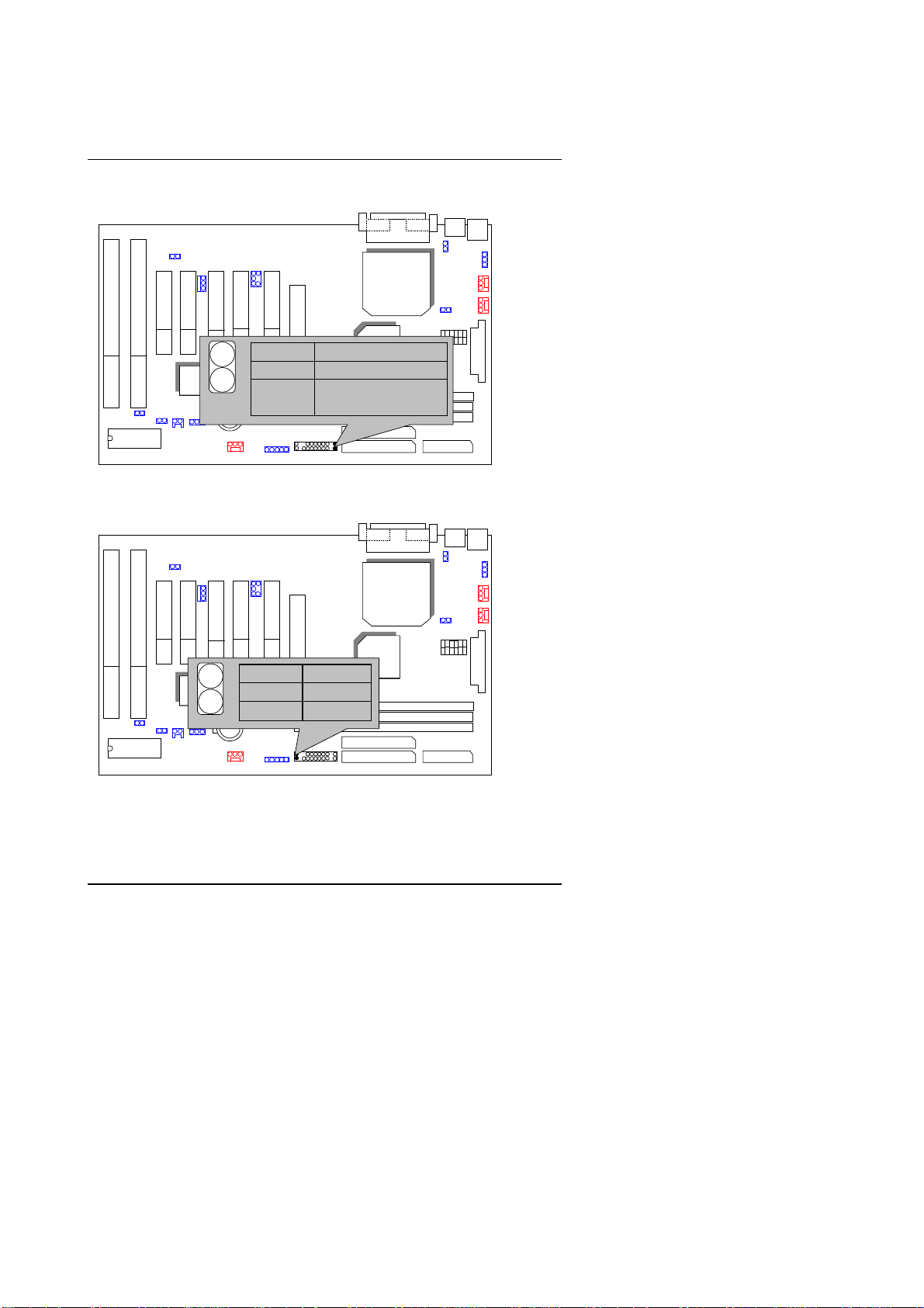
PIN 2: LED cathode (−)
GN: Green Switch
Short: Entering Green Mode
On – Off : For POWER ON or Suspend IN / OUT.
On 4 sec : For POW ER OFF before VGA Enable or
−
PIN 4 : Data (
CMOS setup select “delay 4sec.” For
POW ER OFF mode.
Open: Normal Operation
PIN 1: anode (+)
PIN 1 : VCC (+)
−
)
PIN 1: LED anode (+)
Open: Normal operation
GD: Green Function Active LED
PIN 2: LED cathode (−)
1
PIN 1: LED anode (+)
3-5
Page 44

6VXE7+
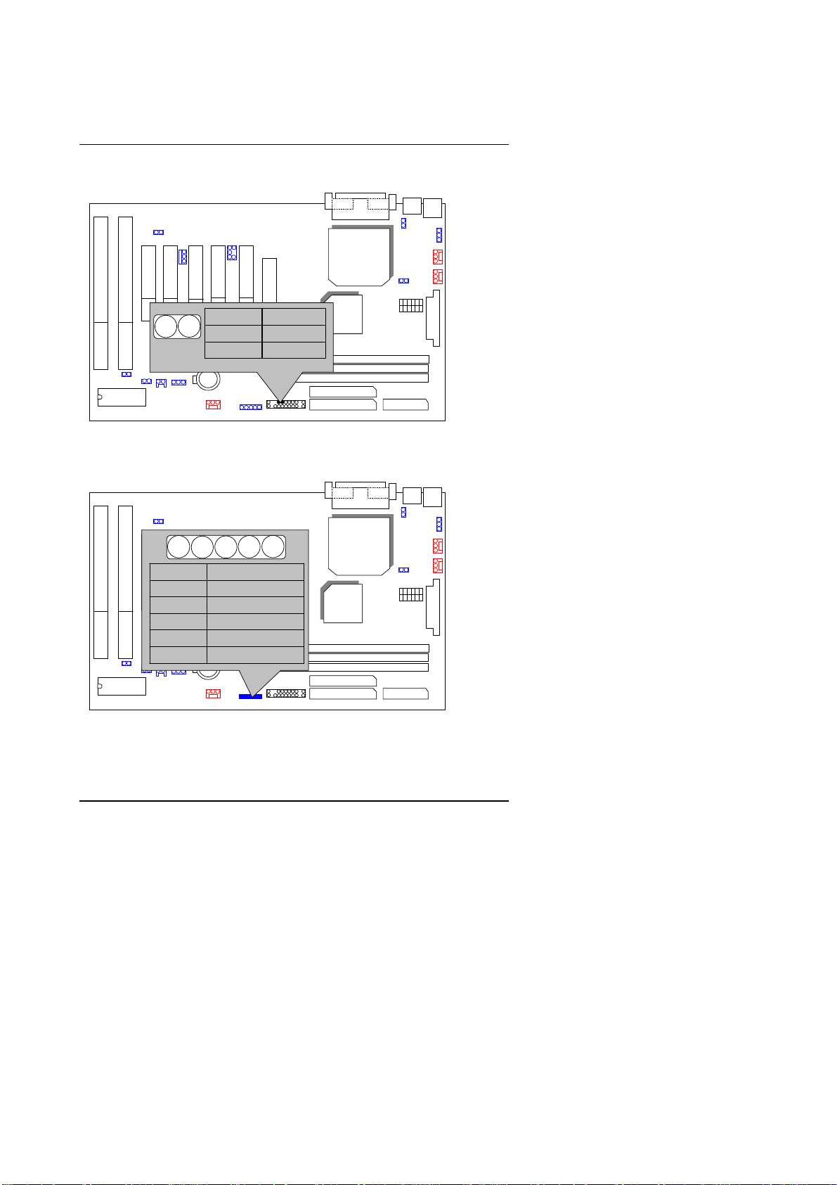
3.4. DRAM INSTALLATION
The Motherboard can be inst alled with 16 / 32 / 64 / 128 / 256 / 512MB (256Mb
Technology) 168 pins DIMM module DRAM, and the DRAM speed must be 67~100
MHz for SDRAM when system bus speed is set to 66MHz. When system bus speed
is set to 100MHz, 100MHz SDRAM is required. The DRAM memory system on
Motherboard consists of bank 0, 1, 2 & bank 3.
Since 168 pins DIMM module is 64 bits width, theref ore 1 piece of DIMM module
may match a 64 bits system. The total memor y size is 16 MB ~ 1.5GMB(256Mb
Techonloy) SDRAM, EDO DRAM size is 16MB ~ 384MB. T he DRAM installation
position refer to Figure 3.1, and notic e the Pin 1 of DIMM modu le mus t mat ch with
the Pin 1 of DIMM s ock et. Insert the DRAM DIMM module into the DIMM socket at
Vertical angle. If there is a wrong direction of Pin 1, the DRAM DIMM module could
not be i nserted into socket com pletely.
3.5. CPU SPEED SETUP
The system bus speed can be set for 66,100,133 MH z. The user can select the
system bus speed
(SW2)
and change the DIP SWITCH
the CPU speed for 500MHz – 1GHz and faster processor.
The CPU speed must match with the frequency RATIO. It will cause system
0000
hanging up if the frequency RATIO is higher than CPU's.
SW1: (O:ON / X:OFF)
FREQ. RATIO
X 3
X 3.5
X 4
X 4.5
X 5
X 5.5
X 6
X 6.5
X 7
X 7.5
X 8
X 8.5
X 9
X 9.5
X 10
X 10.5
1 2 3 4
O X O O
X X O O
O O X O
X O X O
O X X O
X X X O
O O O X
X O O X
O X O X
X X O X
O O X X
X O X X
O X X X
X X X X
O O O O
X O O O
DIP SWITCH (SW)
(SW1)
selection to set up
3-6
Page 45

Hardware Installation
0000
Intel Processor all have locked Frequency Multiple, so you can not change
the CPU Frequency Multiple.
Set System Bus Speed SW2: (O:ON / X:OFF)
CPU PCICLK 1 2 3 4 5 6
66/100/
133/Auto
66 33.3
75 37.5
83 41.6
100 33.3
112 37.3
124 31
133 33.3
140 35
150 37.5
Note: We don’t recommend you to set up your system speed to
0000
75,83,112,124,140 or 150MHz because these frequencies are not the
standard specifications for CPU, Chipset and most of the peripherals.
Whether your system can run under 75,83,112,124,140 or 150 MHz
properly will depend on your hardware configurations: CPU, SDRAM,
Cards, etc.
33.3
X X X X O O
O O X X X X
O O O X X X
O O X O X X
O X X X X X
O X O X X X
X X X O X X
X X X X X X
X X O O X X
X X O X X X
3.6. CMOS RTC & ISA CFG CMOS RAM
There're RTC & CM OS RAM o n board; t hey have a po wer su pply from ex ternal
battery to keep the DATA inviolate & effective. The RTC is a REAL-TIME
CLOCK device, which provides the DATE & TIME to system. The CMOS RAM
is used for ke eping the informat io n of system configuration, so the s ystem can
automatically boot OS every time. Since the lifetime of internal battery is 5
years, the user can change a new Battery to replace old one after it cannot
work.
0
Danger of explosion if battery is incorrectly r eplaced.
0
Replace only with the same or equivalent type recommended by the
manufacturer.
0
Dispose of used batteries according to the manufacturer’s instruction s.
3-7
Page 46

6VXE7+
3.7. SPEAKER CONNECTOR INSTALLATION
There is a speaker in AT system for sound purp ose. The 4 - Pins connector
SPK
is used to connect speaker.
3.8. HARDWARE RESET SWITCH CONNECTOR INS TALLATION
The RESET switc h on pan el pr ovides use rs with HAR DWA RE RESE T func tion.
The system wil l do a cold start after the RESET switch is pushed and release d
by user . The RESET switc h is a 2 PIN connect or and should be ins talled to
on Motherboard.
RST
3.9. POW E R LED CONNECTOR INSTALLATION
System has Power LED lam p on th e pa nel of case. T he P ower LE D wil l light on
off or flash to indicate which st ep on the system. The connector should be
connected to PW of Motherboard in correct dire ction.
3.10. IDE & ATAPI DEVICE INSTALLATION
There are tw o-En h anc ed P CI I DE po rt s (
ATAPI standard SPEC. Any one IDE port can connected to two ATAPI devices
(IDE Hard Disk, CD-ROM & Tape Driver), so total four ATAPI devices can exist
in a system. The
HD
is the active LED port for ATAPI devices.
IDE1, IDE2
) on board, which following
3.11. PERIPHERAL DEVICE INSTALLATION
After the I/O device installation and jumpers setup, the Motherboard can be
mounted into the case and fixed by screw. To complete the Motherboard
installation, the peripheral device could be installed now. The basic system
needs a display interface card. If the PCI - Bus device is to be installed in the
system, any one of four PCI - Bus slots can be used.
3.12. KEYBO ARD & PS/2 MOUSE INSTALLATION
The Motherboard supports PS/2 Mouse. The BIOS will auto detect whether the
PS/2 Mouse is installed or not & assign IRQ12 for PS/2 Mouse port i f i t is
installed. After installing the peripheral device, the user should check
everything agai n, and prepare to power-on the system.
3-8
Page 47

BIOS Configration
4. BIOS CONFIGURATION
Award's BIOS R OM has a bui lt-in S etup program that all ows users to m odify the
basic system confi guration.
This type of information is stored in battery-backed CMOS RAM so that it
retains the Setup i n formation when the power is turned off.
4.1. ENTERING SETUP
Power ON the computer and press <Del> immediately will allow you to enter
Setup.
The other way to enter Setup is t o power on the comput er, when the below
message appears briefly at the bottom of the screen during the POST (Power
On Self Test), press <Del> Key or simultaneously press <Ctrl>, <Alt>, and
<Esc> keys.
Press DEL to enter SETUP.
yyyy
If the message disa ppears b efore you r espond a nd y ou stil l wi sh to ent er Setup ,
restart the system to try again by turning it OFF then ON or pressing the
"RESET" bottom on the system case.
You may also restart by simultaneously press <Ctrl>,<Alt>, and <Del> keys.
4-1
Page 48

6VXE7+
4.2. CONTROL KEYS
Up arrow Move to previous item.
Down arrow Move to next item.
Left arrow Move to the item in the left hand.
Right arrow Move to the item in the right hand.
Esc key Main Menu - Quit and not save changes into CMOS
Status Pag e Setup Menu and Option Pag e Setup Menu -
Exit current page and return to Main Menu.
PgUp key Increase the numeric value or make changes.
PgDn key Decrease the numeric value or make changes.
F1 key General help, only for Status Page Setup Menu and Option
Page Setup Menu.
F2 key Change color from total 16 colors.
F3 key Calendar, only for Status Page Setup Menu.
F4 key Reserved.
F5 key Restore the previous CMOS value from CMOS, only for
Option Page Setup Menu.
F6 key Load the default CMOS value from BIOS default table, only
for Option Page Setup Menu.
F7 key Load the default.
F8 key Reserved.
F9 key Reserved.
F10 key Save all the CMOS changes, only for Main Menu.
4-2
Page 49

BIOS Configration
4.3. GETTING HELP
4.3.1 Main Menu
The on-line description of the highlighted setup function is displayed at the
bottom of the screen.
4.3.2 Status Page Setup Menu / Option Page Setup Menu
Press F1 to pop up a small help wind ow that describe s the appropria te keys to
use and the possible selections for the highlighted item. To exit the Help
Window press <Esc>.
4.4. THE MAIN MENU
Once you enter Award BIOS CMOS Setup Utility, the Main Menu (Figure 4.1)
will appear on the screen.
The Main Menu allows you to select setup functions and exit choices. Use
arrow keys to select among the items and press <Enter> to acce pt or enter th e
sub-menu.
Figure 4.1: Main Menu
Standard CMOS setup
•
This setup page includes all the items in a standard compatible BIOS.
BIOS features setup
•
This setup page includes all the items of Award special enhanced features .
4-3
Page 50

6VXE7+
Chipset features setup
•
This setup page includes all the items of chipse t special features.
Power management setup
•
This setup page includes all the items of Green functi on features.
PNP/PCI configuration
•
This setup page includes all the items of PNP/PCI configuration features.
Load BIOS defaults
•
BIOS defaults indi cates the mo st appropri ate value of the system parameter
which the system would be in safe configuration.
Load Performance defaults
•
Performance Defaults indicates the value of the system parameters which
the system would be in best performance configurati on.
Integrated Peripherals
•
This setup page includes all the items of peripherals features.
Supervisor Password
•
Change, set, o r dis able pass word. I t all ows y ou to li mit ac cess to the sy stem
and Setup, or just to Setup.
User Password
•
Change, set, or disable password. It allows you to limit access to the
system.
IDE HDD auto detection
•
Automatically configure hard disk parameter.
Save & exit setup
•
Save CMOS value changes to CMOS and exit setup.
Exit without save
•
Abandon all CMOS value changes and exit setup.
4-4
Page 51

BIOS Configration
4.5. STANDARD CMOS SETUP
The items in Standard CMOS Setup (Figure 4.2) are divided into 9 categories.
Each category includes no, one or more than one setup items. Use the arrows
to highlight th e item and then use the <PgUp> or <PgDn> keys to select the
value you want in each item.
Figure 4.2: Standard CMOS Setup
Date
•
The date format is < wee k>, < m on th> , <day>, <year>. Pr es s <F3> t o sh ow
the calendar.
Week The week, from Sun to Sat, determined by the BIOS and is
display-only
Month The month, Jan. through Dec.
Day The day, from 1 to 31 (or the maximum all owed in the month)
Year The year, from 1994 through 2079
Time
•
The time format in <hour> <minute> <second>.
The time is calculated base on the 24-hour military -time clock.
For example, 1 p.m. is 13:00:00.
4-5
Page 52

6VXE7+
Primary HDDs / Secondary HDDs
•
The category identify the types of hard disk from drive C to drive F
4 devices that has been instal led in the computer.
There are three options for definable type; User, Auto and None .
Type User is user-de fi nable; and type Auto means automatically detecting
HDD's type and None means No IDE HDD installed.
If you select Type User, related informat ion is asked to be en tered to the
following items.
Enter the information directly from the keyboard and press <Enter>.
Those informa tion sh ould be pr ovided in th e docum entation from y our hard
disk vendor or the system manufacturer.
CYLS. number of cylinders
HEADS number of heads
PRECOMP write precomp
LANDZONE landing zone
SECTORS number of sectors
If a hard disk has not been installed select NONE and press <Enter>.
Drive A / Drive B
•
The category identify the types of floppy disk drive A or drive B that has
been installed in the computer .
None No floppy drive install ed
360K, 5.25 in. 5-1/4 inch PC-type standard drive; 360 kilobyte
capacity.
1.2M, 5.25 in. 5-1/4 inch AT-type high-density drive; 1.2 megabyte
capacity (3-1/2 inch when 3 Mode is Enabled).
720K, 3.5 in. 3-1/2 inch double-sided drive; 720 kilobyte capacity
1.44M, 3.5 in. 3-1/2 inch double-sided dri ve; 1.44 m egab yte capa cit y.
2.88M, 3.5 in. 3-1/2 inch double-sided dri ve; 2.88 m egab yte capa cit y.
4-6
Page 53

BIOS Configration
•
Floppy 3 Mode Support (for Japan A rea)
Disabled Normal Floppy Drive.
Drive A Drive A is 3 mode Floppy Drive.
Drive B Drive B is 3 mode Floppy Drive.
Both Drive A & B are 3 mode Floppy Drives.
Video
•
The category detects the type of adapter used for the primary system
monitor that m u st match your video display card and m onitor.
Although seco ndary monitors are supported, you do not have to select the
type in setup.
EGA/VGA Enhanced Graphics Adapter/Video Graphics Array. For
EGA, VGA, SVGA, or PGA monitor adapters
CGA 40 Color Graphics Adapter, power up in 40 column mode
CGA 80 Color Graphics Adapter, power up in 80 column mode
MONO Monochrome adapter, includes high resolution
monochrome adapters
Halt on
•
The category determines whether the computer will stop if an error is
detected during power up.
NO Errors The system boot will not be stopped for any error
that may be detected
All Errors W henever the BIOS detec ts a non-fatal error, the
system will be stopped and you will be prompted
All, But Keyboard The system boot will not stop for a keyboard error;
it will stop for all other errors
All, But Diskette The system boot will not stop for a disk error; it will
stop for all other errors
All, But Disk/Key The system boot wil l not stop for a keyboard or di sk
error; it will stop for all other errors
4-7
Page 54

6VXE7+
Memory
•
The category is di spl ay -onl y which is determ i ned by POST (Power On S el f
Test) of the BIOS.
Base Memory
The POST of the BIOS will determine the amount of base (or
conventional) memory instal led in the syste m .
The value of the base memory i s typically 512 K for systems with
512 K memory instal led on t he mothe rboard, or 64 0 K for sy stem s
with 640 K or more memory instal led on the motherboard.
Extended Memory
The BIOS determines how much extended memory is present
during the POST.
This is the amount of memory located above 1 MB in the CPU's
memory addr es s map.
Other Memo ry
This refers to the memory located in the 6 40 to 1024 address
space. This is mem or y that can be us ed for di f f ere nt app lications.
DOS uses this area to load device drivers to keep as much base
memory free for application programs. Most use for this area is
Shadow RAM.
4-8
Page 55

BIOS Configration
4.6. BIOS FEATURES SETUP
Figure 4.3: BIOS Features Setup
Virus Warning
•
This category flas hes o n the scr een. During and after t he sy stem boot s up,
any attempt to write to the boot sector or partition table of the hard disk
drive will halt the system and the following error message will appear, in
the mean time, y ou can run anti-virus progr am to locate the problem.
The default value is Disabled.
Enabled
Disabled
•
Processor Number Feature
The default value is Enabled.
Enabled Enable Processor Number Feature.
Disabled Disable Processor Number Feature.
Activate automat ically when the system boots up causing a
warning message to appear when anything attemp ts to
access the boot sector or hard disk partition table.
No warning message appears when anything attempts to
access the boot sector or hard disk partition table.
4-9
Page 56

6VXE7+
•
Boot From LAN First
The default value is Disabled.
Enabled Enable Boot From LAN First.
Disabled Disable Boot From LAN First.
AUTO
•
Boot Sequence
This category determines which drive computer searches first for the disk
operating system (i.e., DOS). Default value is A, C, SCSI.
X1, X2, X3 System will fir st se arch for X 1 di sk dri ve then X 2 di sk d rive
•
VGA Boot From
The default value is AGP
AGP System will boot from AGP Display Card.
PCI Slot System will boot from PCI Slot VGA Card.
•
Boot Up Floppy Seek
During POST, BIOS will dete rmi ne t he fl oppy di sk dri ve i nsta ll ed is 40 or 80
tracks. 360 K type is 40 tracks 720 K, 1.2 M and 1.44 M are all 80 tracks.
The default value is Enabled.
Enabled BIOS searches for floppy disk drive to determine it is 40 or
Disabled BIOS will not search for the ty pe of flopp y disk dri ve by track
Auto detect Boot From LAN First.
and then X3 disk drive.
80 tracks. Note that BIO S can not tell from 720 K, 1.2 M or
1.44 M drive type as they are all 80 tracks.
number. Note that there will not be any warning message if
the drive installed is 360 K.
Boot Up NumLock Status
•
The default value is On.
On Keypad is number key s.
Off Keypad is arrow keys.
4-10
Page 57

BIOS Configration
Memory Parity/ECC Chec k
•
The default value is Disabled.
Enabled Enabled Memory Parity/ECC Check Function.
Disabled Disabled Memory Parity/ECC Check Function.
•
Typematic Rate Setting
The default value is Disabled.
Enabled Enable Keyboard Typematic rate setting.
Disabled Disable Keyboard Typematic rate setting.
•
Typematic Rate (Chars / Sec.)
The default value is 6.
6-30 Set the maximum Typema tic rate from 6 chars. Per second
to 30 characters. Per second.
•
Typematic Delay (Msec.)
The default value is 250.
250-1000 Set the time delay from first key to repeat the same key in
to computer.
Security option
•
The default value is Setup.
Setup The system will boot and access to Setup will be denied if
the correct password is not entered at the prompt.
System The system will not boot and access to Se tup will be denied
if the correct password is not entered at the prompt.
0000
To disable secur ity, select PASSWORD S ETTING at Main Menu and then
you will b e asked to ent er pas sword . I f the u ser d oes no t ty p e any thing and
just press <E nter>, i t wil l disabl e secur ity. Once the security is disabl ed, the
system will boot and you can enter Setup freely.
4-11
Page 58

6VXE7+
PCI/VGA Palette Snoop
•
The default value are Disabled.
Enabled For having Video Card on ISA Bus and VGA Card on PCI
Bus.
Disabled For VGA Card only.
•
Assign IR Q Fo r VGA
The default value is Enabled.
Enabled Assign IRQ For VGA
Disabled Not assign IRQ For VGA
HDD S.M.A.R.T. Capability
•
The default value is Disable.
Enable Enable HDD S.M.A.R.T. Capability
Disable Disable HDD S.M.A.R.T. Capability
•
Report No FDD For WIN 95
The default value is No.
No Assign IRQ6 For FDD.
Yes FDD Detect IRQ6 Automaticall y.
4-12
Page 59

4.7. CHIPSET FEATURES SETUP
BIOS Configration
Figure 4.4: Chipset Features Setup
•
Top Performance
The default value is Disabled.
Enabled
Disabled Disabled Top Performance.
SDRAM Cycle Length
•
The default value is 3.
Auto Set SDRAM Cycle Length is Auto
3 For Slower SDRAM DIMM module.
2 For Fastest SDRAM DIMM module.
•
DRAM Clock
The default value is Host CLK
CPU CLK DRAM CLK
100,112,124,133,140,150 Host CLK.
Enabled Top Performance.
Host CLK 66,75,83
Host CLK +33M
4-13
Page 60

6VXE7+
•
Read Around write
The default value is Enabled.
Enabled
Disabled Normal operation.
Concurrent PCI/Host
•
The default value is Disabled.
Enabled
Disabled Disabled Concurrent PCI/Host.
•
AGP Aperture Size
The default value is 64MB
64MB Set AGP Aperture Size to 64MB.
32MB Set AGP Aperture Size to 32MB.
16MB Set AGP Aperture Size to 16MB.
8MB Set AGP Aperture Size to 8MB.
4MB Set AGP Aperture Size to 4MB.
128MB Set AGP Aperture Size to 128MB.
•
Power LED in Suspend
The default value is BLINKING
BLINKING Set Power LED in Suspend at BLINKING mode.
ON Set Power LED in Suspend at ON mode.
OFF/DUAL Set Power LED in Suspend at OFF/DUAL mode, if you
When set Enabled this feature speeds up data read
performance.
Enabled Concurrent PCI/Host.
use a dual color power LED , it will show dual color.
•
Spread Spectrum
The default value is Disabled.
Disabled Spread Spectrum Disabled
Enabled Set Spread Spectrum Enabled.
4-14
Page 61

4.8. POW E R MANAGEMENT SETUP
BIOS Configration
Figure 4.5: Power Management Setup
✼
These two items will show up when “RTC Alarm Resume” is enabled.
•
Power Management
The default value is Enabled.
Enabled For configuring our own power management features.
Min Saving Enable Green function.
Max Saving Disable Green function.
•
Video Off Method
The default value is DPMS Support.
V/H SYNC + Blank BIOS will turn off V/H-SYNC when gets into
Green mode for Green monito r power saving.
Blank Screen BIOS will only black monitor when gets into
Green mode.
DPMS Support BIOS will use DPMS Standar d to cont rol VGA
card. (The Green type VGA card will turn of
V/H-SYNC automatically.)
4-15
Page 62

6VXE7+
•
Soft-off by PWRBTN
The default value is Instant-off.
Instant-off Soft switch ON/OFF for power ON/OFF.
Delay 4 sec Soft switch on 4sec for power OFF.
•
System After AC Back
The default value is Soft-Off.
Memory This function depends on computer status
Soft-Off Set System Soft-Off Status.
Full-On Set System Full-On Status.
•
CPU FAN In Suspend
The default value is Off.
On Disable this functi on.
Off Stop CPU FAN when entering Suspend mode.
•
HDD Power Down
The default value is Disabled.
Disabled Disabled HDD Power Down mode funct ion.
1-15 mins. Enabled HDD Power Down mode between 1 to 15 mins.
•
Suspend Mode
The default value is Disabled.
Disabled Disabled Suspend Mode.
10 Sec - 1 Hour Setup the timer to enter Suspend Mode.
•
VGA
The default value is OFF.
OFF Disable monitor VGA activity.
ON Enable monitor VGA activity.
4-16
Page 63

•
LPT & COM
The default value is LPT/COM.
LPT/COM Enabled LPT/COM Ports Activity.
NONE Normal Operation.
LPT Enabled LPT Ports Activity.
COM Enabled COM Ports Activity.
•
HDD & FDD
The default value is ON.
ON Enabled HDD & FDD Ports Activity
OFF Disabled HDD & FDD Ports Activity
•
DMA/master
The default value is OFF.
ON Don’t detect DMA/master PM event.
OFF Normal Operation.
•
Wake Up On RI#
The default value is Enabled.
Enabled
Disabled Disable Wake Up On LAN/Ring
Enable Wake Up On LAN/Ring
BIOS Configration
•
Wake Up On PME#
The default value is Enabled.
Enabled
Disabled Disable Wake Up On PME#
Enable Wake Up On PME#
4-17
Page 64

6VXE7+
•
RTC Alarm Resume
You can set “RTC Alarm Re sume” item to Enabled and key in date/time to
power on system. The default value is Disabled.
Disabled Disabl e this function.
Enabled Enable alarm function to POWER ON system.
If the “RTC Alarm Resum e ” is Enabled.
Date ( of Month) Alarm : 0~31
Time ( hh: mm: ss) Alarm : (0~23) : (0~59) : (0~59)
•
Primary INTR
The default value is ON.
ON Primary INTR function is on.
OFF Normal Operation.
•
IRQ [3~15]
The default value is Primary/Secondary/Disabled.
Disabled Disabl e this function.
Primary The resource is used by Primary device .
Secondary The resource is used by Secondary device .
4-18
Page 65

BIOS Configration
4.9. PNP/PCI CONFIGURATION
Figure 4.6: PNP/PCI Configuration
0
IRQ[3.4.5.7.9.10.11.12.14.15 ] & DMA[0. 1 .3.5.6.7]These item s wil l show up
when “Resources Controlled By” is Manual.
•
PNP OS Installed
The default value is No.
Yes Enable PNP OS Installed function.
No Disable PNP OS Installed function.
•
Resources Controlled by
The default value is Auto.
Manual User can set the PnP resource (I/O Address, IRQ & DMA
channels) used by legacy ISA DEVICE.
Auto BIOS automatically use these PnP rescuers.
•
Reset Configuration Data
The default value is Disabled.
Disabled Disable this function.
ESCD Enable clear PnP information in ESCD.
DMI Enable clear PnP information in DMI.
BOTH Enable clear PnP information in ESCD and DMI.
4-19
Page 66

6VXE7+
•
IRQ (3,4,5,7,9,10,11,12,14,15), DMA (0,1,3,5,6,7) assigned to
The default value is "Legacy ISA" or "PCI/ISA PnP".
Legacy ISA The re so urce is used by L egacy ISA device.
PCI/ISA PnP The resource is used by PCI/ISA PnP device (PCI or ISA).
•
Assign IRQ For USB
The default value is Enabled.
Enabled Assign a specific IRQ for USB.
Disabled No IRQ is assigned for USB.
4-20
Page 67

4.10. LOAD BIOS D E FAULTS
Figure 4.7: Load BIOS Defaults
Load BIOS Defaults
•
To load BIOS defaults value to CMOS , enter "Y". If not, enter "N".
BIOS Configration
4-21
Page 68

6VXE7+
4.11. LOAD PERFORMANCE DEFAULTS
Figure 4.8: Load Performance Defaults
Load Performance Defaults
•
To load Performance defaults value to CMOS , enter "Y". If not, enter "N".
If there is any problem occurred, loading PERFORMANCE DEFAULTS
0000
step is recommended.
4-22
Page 69

BIOS Configration
4.12. INTEGRATED PERIPHERALS
**
*
Figure 4.9: Integrat ed peripherals
**
This items wil l show up when ”UART2 Mode Select” i s set to IrDA 1.0or
ASKIR.
* This item wil l show up when “Keyboard Power On: Mu ltikey” is sel ected.
USB Controller
•
The default value is Enabled.
Enabled Enabled USB Controller.
Disabled Disabled USB Controller.
•
USB Key board Support
The default value is Disabled.
Enabled Enabled USB Keyboard Support.
Disabled Disabled USB Keyboard Support.
4-23
Page 70

6VXE7+
Onboard Serial Port 1
•
The default value is 3F8/IRQ4.
Auto BIOS will automatical ly setup the port 1 address.
3F8/IRQ4 Enable onboard Serial port 1 and address is 3F8.
2F8/IRQ3 Enable onboard Serial port 1 and address is 2F8.
3E8/IRQ4 Enable onboard Serial port 1 and address is 3E8.
2E8/IRQ3 Enable onboard Serial port 1 and address is 2E8.
Disabled Disable onboard Serial port 1.
•
Onboard Serial Port 2
The default value is 2F8/IRQ3.
Auto BIOS will automatical ly setup the port 2 address.
3F8/IRQ4 Enable onboard Serial port 2 and address is 3F8.
2F8/IRQ3 Enable onboard Serial port 2 and address is 2F8.
3E8/IRQ4 Enable onboard Serial port 2 and address is 3E8.
2E8/IRQ3 Enable onboard Serial port 2 and address is 2E8.
Disabled Disable onboard Serial port 2.
•
Onboard Parallel port
The default value is 378/IRQ7.
378/IRQ7 Enable onboard LPT port and address is 378/IRQ7.
278/IRQ5 Enable onboard LPT port and address is 278/IRQ5.
3BC/IRQ7 Enable onboard LPT port and address is 3BC/IRQ7.
Disabled Disable onboard LPT port.
•
Parallel Port Mode
The default value is SPP.
SPP Using Parallel port as Standard Parallel Port.
EPP Using Parallel port as Enhanced Parallel Port.
ECP Using Parallel port as Extended Capabilities Port.
ECP+EPP Using Parallel port as ECP & EPP mode.
4-24
Page 71

BIOS Configration
UART2 Mode
•
(This item allows you to determine which UART2 Mode of onboard I/ O
chip), the default val ue is Standard.
ASKIR Set onboard I/O chip UART2 to ASKIR Mode.
IrDA 1.0 Set onboard I/O chip UART2 to IrDA Mode.
Standard Set onboard I/O chip UART2 to Standard Mode.
UART2 Duplex Mode
•
The default value is Half.
Half Set UART2 Duplex Mode to Half.
Full Set UART2 Duplex Mode to Full.
•
PS/2 Mouse Power on
The default value is Disabled.
Disabled Disable PS/ 2 Mouse Power on .
Db Click Double click PS/2 Mouse bottom.
•
Keyboard Power on
The default value is POWER Key.
POWER Key
Multi key Enter multikey combination to Power on system.
If your keyboard have “POWER Key” butt on, you can
press the key to power on your system.
KB Power On Password
•
Enter
Enter from 1 t o 5 char act ers t o set the Key board Po wer On
Password.
4-25
Page 72

6VXE7+
4.13. SUPERVISOR / USER PASSWORD
When you select this function, the following message will appear at the center
of the screen to assist you i n creating a password.
Figure 4.10: Password Setting
Type the password, up to eight characters, and press <Enter>. You will be
asked to confirm the password. Type the password again and press <Enter>.
You may also press <Esc> to abort the selection and not enter a password.
To disable password, just press <Enter> when you are prompted to enter
password. A message “
password being disabled. Once the password is disabled, the system will boot
and you can enter Setup freely.
The BIOS Setup program allows you to specify two separ ate passwords: a
SUPERVISOR PASSWORD
anyone may access all BIOS Setup program function. When enabled, the
Supervisor password is required for entering the BIOS Setup program and
having full configuration fields, the User password is required to access only
basic items.
If you select “Sy st em” at “
will be prom pted for the pass word e very time the sy stem i s reboo ted or any time
you try to enter Setup Menu.
If you select “Setup” at “
will be prompted only when you try to enter Setup.
PASSWORD DISABLED
USER PASSWORD
and a
Security Option
Security Opt io n
” in BIOS Fe atu res Setup Menu, y ou
” in BIOS Features Setup Menu, you
” will appear to confirm the
. When di s a bl e d ,
4-26
Page 73

4.14. IDE HDD AUTO DETECTION
BIOS Configration
Figure 4.11: IDE HDD Auto Detection
Type "Y" will accept the H.D.D. parameter reported by BIOS.
Ty pe "N" wi ll keep the old H. D.D. par am eter setup. If t he h ard disk cylinde r NO .
is over 1024, then the user can select LBA mode or LARGE mode for DOS
partition larger than 528 MB.
4-27
Page 74

6VXE7+
4.15. SAVE & EXIT SETUP
Figure 4.12: Save & Exit Setup
Type "Y" will quit the Setup Utility and save the user setup value to R TC
CMOS .
Type "N" will return to Setup Utility.
4-28
Page 75

BIOS Configration
4.16. EXIT WITHOUT SAVING
Figure 4.13: Exit Without Saving
Type "Y" will quit the Setup Utility without saving to RT C CMOS .
Type "N" will return to Setup Utility.
4-29
Page 76

Page 77

6VXE7+
Appendix A : VIA Chipsets Driver Installation
A.VIA 4 in 1 Service Pack Utility:
Insert the support CD that came with your motherboard into your CD-ROM driver or double –click
the CD driver icon in My Computer to bring up the screen.
1.Click “VIA 4in 1 Service Pack
Utility” item.
(1)
(2)
2.Click “Yes”.
(3)
4.Click “Next”.
(5)
A-1
3.Click “Next”.
(4)
5.Click “Next”.
(6)
Page 78

Appendix
6.Click “Next”.
(7)
8.Click “Next”.
(9)
9.Click “Finish” to
restart computer.
7.Click “Next”.
(8)
(10)
A-2
Page 79

6VXE7+
Appendix B: BIOS Flash Procedure
BIOS update procedure:
If your OS is Win9X, we recommend that you used Gigabyte @BIOS Program
to flash BIOS.
Click “Tool” .
Click “@BIOS Writer v1.05”
Click “9” .
Click Here.
Methods and steps :
I. Update BIOS through Internet
a. Click "Internet Update" icon
b. Click "Update New BIOS" icon
c. Select @BIOS sever ( "Gigabyte @BIOS sever 1 in Taiwan" and
"Gigabyte @BIOS sev er 2 in Taiwan" are availabl e for now , th e others
will be completed soon)
d. Select the exact model name on your motherboard
e. System will automatically download and update the BIOS.
A-3
Page 80

II. Update BIOS NOT through Internet :
a. Do not click "Internet Update" icon
b. Click "Update New BIOS"
c. Please select "All Files" in dialog box while opening the ol d file.
d. Please search for BIOS unzip file, downloadi ng from internet or any
III. Save BIOS
IV. Check out supported motherboa rd and Flash ROM :
Note :
other methods (such as: 6OXM7E.F1).
e. Complete update process following the instruction.
In the very beginning, there is "Save Current BIOS " icon shown in dialog
box. It means to save the current BIOS version.
In the very beginning, there is "About thi s program" icon shown in dialog
box. It can help you che ck out which kind of motherb oard an d which brand
of Flash ROM are supported.
a. In method I, if it shows t wo or more mo therboard 's model nam es to be
selected, please make sure your motherboa rd's model name agai n.
Sellecting name will cause the sy stem unbooted.
b. In method II, be sure that mot herboard's model nam e in BIOS unzip
file are the same as your motherboard's. Otherwise, your system
won't boot.
c. In method I, if the BIOS file you need cannot be found in @BIOS
server, please go onto Gigabyte's web site for downloading and
updating it according to method II.
d. Please note that any intercorrupt ion during updati ng will cause
system unbooted
Appendix
A-4
Page 81

6VXE7+
Or else you can select flash BI OS in DOS mode.
0
Please check your
name
PCB
and
version
1. Format a bootable system floppy diskette by the command “
2. Visit the Gigabyt e website at http:// www.gigabyte.com.tw
3. Insert the bootable diskette containing the BIOS file into the floppy
4. Assuming that the floppy diskette dri ver is A, reboot the syst em by
5. Upon pressing the <Enter> key, a flash memory writer menu will
on the motherboard.
a:/s
” in command mode.
BIOS file you need and downl oad it to your bootab le floppy diskette.
diskette driver.
using the A: driver. At the A: > prompt, run the BIOS upgraded file by
executing the Flash BIOS utility and the BIOS file with its appropriate
extension.
Example:
Example:
appear on screen. Enter the new BIOS file name with its extension
filename into the text box after file name to program.
BIOS vendor (AMI or AWARD)
(AMI tool)
(Award tool )
(Where 6VXE7P.f1 is name of the BIOS file name)
A:>
flashxxx.exe 6
(Where 6VXE7P.f1 is name of the BIOS file name)
A:>wdflash. exe 6
VXE7P
VXE7P
.f1
.f1
,your
motherboard
format
,Select the
6. If you want to save the old BIOS file(perform as soon as system is
operational, this is recommended), select Y to
SAVE BIOS
filename to save: This option allows you to copy the contents of the
flash memory chip onto a diskette, giving you a backup copy of the
original mot herboard BI OS in case y ou need to re-i nstall it. Select N to
DO YOU WANT T O SAVE BIOS
BIOS file.
, then type the old BIOS filename and the extension after
, if you don’t want to save the old
A-5
DO YOU WANT TO
Page 82

7. After the decision to save the old BIOS file or not is made, select Y to
ARE YOU SURE TO PROGRAM
until a message showing Power Off or Reset the system appea rs.
Then turn off your system.
8. Remove the diskette and restart your system.
9. Hold down <Delete> key to enter BIOS setup. You must select “Load
Setup BIOS De fault” to acti vat e th e ne w BI OS, t hen y ou m ay set other
item from the main menu.
when the next menu appear; wait
Appendix
A-6
Page 83

Per FCC Part 2 Section 2. 1 077(a)
FCC Compliance Statement:
This equipment has been tested and found to
Responsible Party Name: G.B.T. INC.
Phone/Fax No: (81 8) 854-9338/ (818) 854-9339
hereby declares that the product
Product Name:
Model Number:
Conforms to the following specifications:
FCC Part 15, Su bpart B, Section 15. 107(a) and Section 15 .109(a),
Class B Digital Device
Supplementary Informatio n :
This device complies with part 15 of the FCC Rules. Ope ration is subject to the
following two conditions: (1) This device may not cause harmful
and (2) this device must accept any inference received, including
that may cause un desired operation.
Representative Person's Name: ERIC LU
Signature:
Address: 18305 V alley Blvd., Suite#A
Mother Board
Date: Mar. 16, 2000
LA Puent, CA 91744
GA-6VXE7+
Eric L u
comply with limits for a Class B digital device ,
pursuant to Part 15 of the FCC rules. These
limits are designed to provide reasonable
protection against harmful interference in
residential installations. This equipment
generates, uses, and can radiate radio
frequency energy, and if not installed and used
in accordance with the instructions, may cause
harmful interference to radio communications.
However, there is no guarantee that
interference will not occur in a particular
installation. If this equipment does cause
interference to radio or television equipment reception, which can be
determined by turning the eq uipmen t off and on, t he user is enco uraged to try to
correct the interference by one or more of the followi ng measures:
-Reorient or relocate the receiving antenna
-Move the equipment away from the receiver
-Plug the equip ment into an outle t on a circuit different fro m that to which
the receiver is connected
-Consult the dealer or an experienced radio/television te chnician for
additional sugge stions
You are cautioned that any change or modifications to the equipment not
expressly approve by the party responsible for compliance could void Your
authority to operate such equipment.
This device complies with Part 15 of the FCC Rules. Operation is subjected to
the following two conditions 1) this device may not cause harmful interference
and 2) thi s de vice must a ccept any inter ferenc e re ceive d, i ncl udin g int erfer ence
that may cause undesired operation.
Page 84

Declaration of Conformity
We, Manufacturer/Importer
G.B.T. Technology Trading GMBH
Ausschlager Weg 41, 1F, 20537 Hamburg, Germany
( description of the apparatus, system, installation to which it refers)
(reference to the specification under which conformity is declared)
Limits and methods of measurement
EN 55011
of radio disturbance characteristics of
industrial, scientific and medical (ISM electrical equipment “Harmonics”
high frequency equipment
Limits and methods of measurement
EN55013
of radio disturbance characteristics of
broadcast receivers and associated electrical equipment “Voltage fluctuati ons”
equipment
Limits and methods of measurement
EN 55014
of radio disturbance characteristics of
portabl e t ool s an d s imilar el ec t r ical
apparatus Residual, commercial and light i ndust ry
EN 55015
of radio disturbance characteristics of Industrial environment
fluorescent lamps and luminaries
EN 55020
broadcast receivers and associated Industrial environment
equipment
EN 55022
of radio disturbance characteristics of appliances tools and similar apparatus
information technology equipment
DIN VDE 0855
part 10
part 12
household electrical appliances,
Limits and methods of measurement
Immunity from radio interference of
Limits and methods of measurement
Cabled distribution systems; Equipment
for receivi ng and/or
sound and television signals
declare that the product
in accordance with 89/336 EEC-EMC Directive
from power systems (UPS)
distribution
(full address)
Mother Board
GA-6VXE7+
is in conformity with
EN 61000-3-2*
EN60555-2
EN61000-3-3*
EN60555-3
EN 50081-1
EN 50082-1
EN 55081-2
EN 55082-2
ENV 55104
EN 50091- 2
Disturbances in supply syst ems caused
by household appliances and similar
Disturbances in supply systems caused
by household appliances and similar
Generi c emission standard Part 1:
Residual, commercial and light industry
G e ner ic immuni ty st an d ar d Pa r t 1:
Generic emission standard Part 2:
G e ner ic immuni ty st an d ar d Pa r t 2:
Immunity requirements for household
EMC requirements for uninterruptible
CE marking
The manufacturer also declares the conformity of above mentioned product
Safety requirements for mains operated
EN 60065
electronic and related apparatus for including electrical business equipment
household and similar general use
Safety of household and similar
EN 60335
electrical appliances uninterruptible power systems (UPS)
Signature
with the actual required safety standards in accordance with LVD 73/23 EEC
Manufacturer/Importer
Date : Mar. 16 ,2000 Name : Rex Lin
(Stamp)
(EC conformity marking)
Safety for information technology equipment
EN 60950
G e ner a l an d S af ety requ i rements for
EN 50091-1
Rex Lin
:
 Loading...