

Page 1

GS1572
A Guide to Designing with the GS1572 (EB1572)
Reference Design
GS1572 A Guide to Designing with the GS1572
(EB1572)
Reference Design
46282 - 1 November 2009
www.gennum.com
1 of 18
Proprietary & Confidential
Page 2

Revision History
Version ECR Date Changes and/or Modifications
1 153754 November 2009 Updated to latest Gennum template.
0 146806 August 2007 New document.
Contents
Revision History ................................................................................................................................................. 2
1. Overview.......................................................................................................................................................... 3
2. Design and Layout Guide ........................................................................................................................... 4
2.1 Power Supply and Ground Isolation ..........................................................................................4
2.1.1 Isolation Methods .................................................................................................................4
2.2 Serial Digital Outputs ...................................................................................................................... 5
2.3 VCO Power ......................................................................................................................................... 6
3. Evaluation Board User’s Guide .................................................................................................................7
3.1 Power .................................................................................................................................................... 7
3.2 Inputs ....................................................................................................................................................7
3.3 Outputs ................................................................................................................................................ 8
3.4 Modes of Operation .........................................................................................................................9
3.5 External Control Interface .......................................................................................................... 10
4. Board Schematic ......................................................................................................................................... 11
5. Board Layout................................................................................................................................................ 13
6. Bill of Materials............................................................................................................................................ 15
7. Recommended Components .................................................................................................................. 17
8. References..................................................................................................................................................... 18
GS1572 A Guide to Designing with the GS1572
(EB1572)
Reference Design
46282 - 1 November 2009
2 of 18
Proprietary & Confidential
Page 3

1. Overview
GO1555
(VCO)
GS1572
Parallel
Input
and
PCLK
Serial
Output
This document serves as a reference for designing with the GS1572. It uses the GS1572
evaluation board as a guide. The document is separated into two main sections:
1. Recommended PCB layout practices when designing with the GS1572.
2. A user’s guide to the GS1572 evaluation board, including information on how to use
the board, and detailed schematic and board layout information.
An example of a board design including the GS1572 is shown below. A 10-bit or 20-bit
signal at HD or SD rates must be supplied, along with a parallel clock. The serialized
output is driven by an internal cable driver. The output is fed to BNC’s.
The GS1572 also requires the external GO1555 VCO.
Figure 1-1: GS1572 Block Diagram
GS1572 A Guide to Designing with the GS1572
(EB1572)
Reference Design
46282 - 1 November 2009
3 of 18
Proprietary & Confidential
Page 4

2. Design and Layout Guide
The following sections describe recommended PCB layout practices to optimize the
performance of the GS1572. All layout recommendations discussed in this section are
used on the GS1572 evaluation board. For information on the GS1572, please see
Evaluation Board User’s Guide on page 7.
2.1 Power Supply and Ground Isolation
The GS1572 requires two voltages, +3.3V and +1.8V. The +1.8V feeds the digital core,
phase detector and optionally, the digital I/O. The +3.3V feeds the on-chip regulator for
the external VCO and the SDI cable driver. Optionally, the I/O may also use the +3.3V
supply. For optimal performance, it is essential that these supplies be isolated to avoid
external noise coupling. The supplies can be broken down into four components:
1. +1.8V ANALOG - supplying power to the following pins on the GS1572:
PD_VDD/PD_GND (pins A6, B6 and C6, C7, C8)
2. +1.8V DIGITAL - supplying power to the following pins on the GS1572:
CORE_VDD/CORE_GND (pins A5, E1, G10, K8 and B5, C5, D5, E2, E5, E6, E7, F4,
F5, F6, F7, G9, J8)
3. +3.3V ANALOG - supplying power to the following pins on the GS1572:
CP_VDD/CP_GND, CD_VDD/CD_GND (pins A10 and B10, E10 and C9, D9, E9,
F9)
NOTE: Power should be removed from CD_VDD in STANDBY mode for
additional power savings.
4. +3.3V DIGITAL: - supplying power to the following pins on the GS1572:
IO_VDD/IO_GND (pins G1, H10 and G2, H9)
NOTE: Optionally, 3.3V digital can be replaced with 1.8V digital to run with 1.8V
IO.
2.1.1 Isolation Methods
Because of the noise sensitive nature of the PLL and analog components of the GS1572,
an isolation technique should be used to filter power to these sections.
Figure 2-1 shows the basic concept behind the technique used. The power plane and
ground plane are isolated from the main plane by a ‘moat.’ Power and ground
connections to the ‘islands’ are made through ferrite beads (0
decoupled on both sides. If possible, running high-speed traces across the moat should
be avoided. Also, any copper (i.e. planes or pours on other layers) which bridge the moat
should be removed.
Ω resistors) which are
GS1572 A Guide to Designing with the GS1572
(EB1572)
Reference Design
46282 - 1 November 2009
4 of 18
Proprietary & Confidential
Page 5

Figure 2-1: Power Supply Isolation Method
ISOLATED
PLANE
+
VIA TO GROUND
VIA TO POWER
GROUND PLANE
POWER PLANE
FB
FB
+
POWER PLANE
GROUND PLANE
VIA TO POWER
VIA TO GROUND
MAIN PLANE
Plane Layer,
Negative Image
Power and Ground
Plane Voids
2.2 Serial Digital Outputs
The serial digital differential outputs are designed to be SMPTE compliant for voltage
level, rise/fall time and return loss specifications. Figure 2-2 shows the recommended
SDO layout and component placement. Ground and power plane voids are placed
under the ORL matching network. The cutouts under the pull-up resistors attached to
the output pins are necessary and are used to reduce the capacitance and provide better
matching to the 75
Additional points relating to SDO layout and component placement (Figure 2-2):
1. Place the pull-up resistors close to the SDO and SDO pins of the GS1572.
2. Try to avoid running high speed traces through vias.
.
Ω transmission line.
Figure 2-2: Recommended Layout of SDO Section of PCB
GS1572 A Guide to Designing with the GS1572
(EB1572)
Reference Design
46282 - 1 November 2009
Proprietary & Confidential
5 of 18
Page 6

2.3 VCO Power
Plane Layer,
Negative Image
Gennum’s external GO1555 VCO is required for operation of the GS1572. VCO_VCC
(pin A8) and VCO_GND (pins B8 and B9) are provided by the GS1572’s internal regulator
and supply +2.5V to the GO1555. The +2.5V is derived from the +3.3V ANALOG
connection to CP_VDD (pin A10) and CP_GND (pin B10) of the GS1572.
Figure 2-3 shows the connection to the VCO supply and Figure 2-4 shows the
recommended PCB layout and component placement. Note that isolation is complete
and the only connection to the VCO plane is through the VCO_VCC and VCO_GND pins.
NOTE: Do not externally apply voltages to the VCO_VCC and VCO_GND pins.
+3.3V
+
GND
FB
+
FB
CP_GND
Figure 2-3: Connection of GS1572 to VCO Supply
Figure 2-4: Recommended VCO Layout
CP_VCC
VOLTAGE REGULATOR
VCO_VCC
GO1555
VCO_GND
GS1572 A Guide to Designing with the GS1572
(EB1572)
Reference Design
46282 - 1 November 2009
6 of 18
Proprietary & Confidential
Page 7
3. Evaluation Board User’s Guide
The GS1572 board demonstrates the operation of the GS1572, allowing control of input
signals and probing of output signals from the device. In addition to the GS1572, the
GS1572 uses the GO1555 Voltage Controlled Oscillator.
A 10-bit or 20-bit signal at HD or SD rates must be supplied, along with a parallel clock.
The serialized output stream is made available on the output.
The board contains headers and leads allowing output signals to be easily probed and
chip features to be enabled. It also provides a JTAG interface and access to the GS1572’s
internal registers via the Gennum Serial Peripheral Interface (GSPI). A push button
allows the board to easily be reset.
3.1 Power
The GS1572 evaluation board requires a +5V power supply and a ground connection.
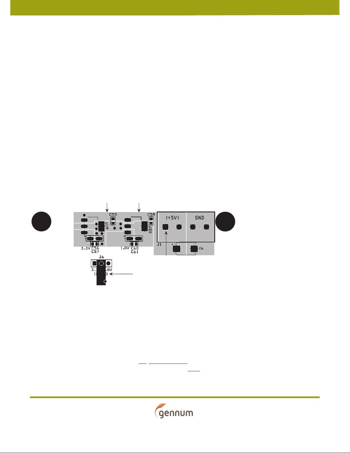
Power regulation to +3.3V and +1.8V is done on board (see Figure 3-1).
Power supply and ground isolation on the GS1572 is based on the recommendations
discussed in Power Supply and Ground Isolation on page 4.
ON BOARD
POWER REGULATORS
POWER BLOCK
CONNECT +5VDC HERE
I/O VOLTAGE SELECTION
Figure 3-1: Power Block
3.2 Inputs
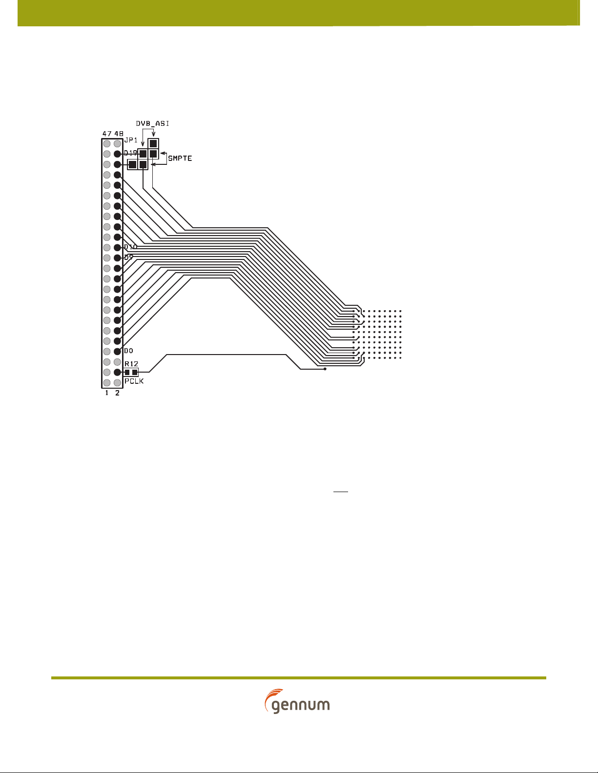
The GS1572 evaluation board includes a 48 pin parallel input connector. Twenty pins of
the connector are used for the 20-bit input of the GS1572, DIN [19:0]. An additional bit
connects to the PCLK input pin of the GS1572 (see Figure 3-2). For more information on
the function of these pins, please refer to the GS1572 Data Sheet. The remaining 27 bits
of the parallel bus connect to ground.
The input format is defined by setting the SD/HD
jumpers. The input data bus width is controlled by setting the 20bit/10bit
GS1572 A Guide to Designing with the GS1572
(EB1572)
Reference Design
46282 - 1 November 2009
, SMPTE_BYPASS, and DVB_ASI
jumper. Modes
7 of 18
Proprietary & Confidential
Page 8
of Operation on page 9 describes the setting of these jumpers to serialize specific input
INPUT BUS
DIN[19:0]
PCLK
INPUT
data formats.
The LOCK LED on the GS1572 indicates the status of the LOCKED pin on the GS1572. The
LED will be on whenever the GS1572 PLL is locked to PCLK.
Figure 3-2: Parallel Input Bus
3.3 Outputs
The GS1572 contains an integrated serial digital cable driver (see Figure 3-3) to
guarantee SMPTE return loss specifications are met at HD rates.
The output signal may be enabled or disabled by setting the SDO_EN/DIS
GS1572 A Guide to Designing with the GS1572
(EB1572)
Reference Design
46282 - 1 November 2009
jumper.
8 of 18
Proprietary & Confidential
Page 9
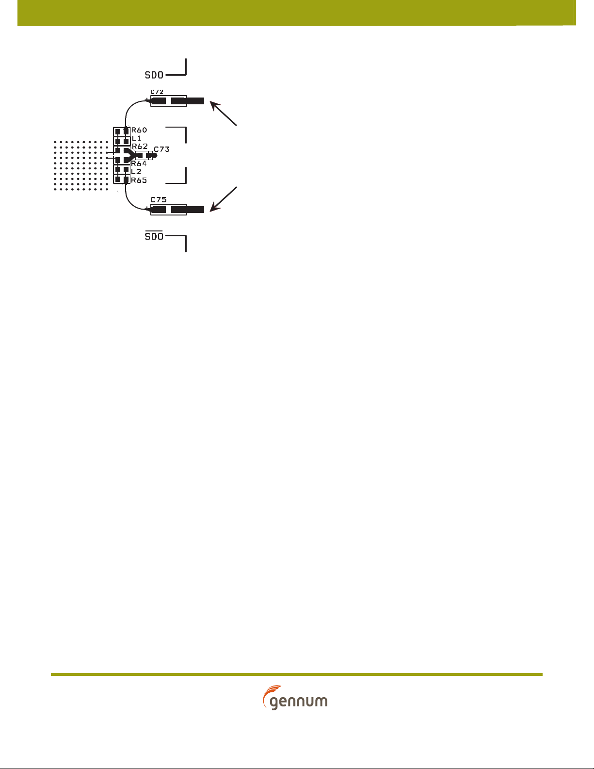
Figure 3-3: Output Block
SERIAL DIGITAL
DIFFERENTIAL
OUTPUTS
3.4 Modes of Operation
The GS1572 has three basic modes of operation which determine what processing the
input data will undergo prior to serialization.
SMPTE MODE — The input data will be scrambled according to SMPTE 259M and 292M,
and encoded prior to serialization.
DVB-ASI MODE — All SMPTE processing features are disabled, and the 8-bit transport
stream data will be 8b/10b encoded prior to serialization.
DATA-THROUGH MODE — The device operates as a simple parallel-to-serial converter.
Input data is serialized and presented to the output buffer without any prior scrambling
or encoding.
Table 3-1 gives a description of the GS1572 jumper settings in each mode.
NOTE: The jumpers correspond directly to pins on the GS1572. Please see the GS1572
Data Sheet for a more detailed explanation of the operation of these pins in each mode.
Depending on the mode of the GS1572, the SMPTE or DVB_ASI jumpers on the GS1572
must be set appropriately (see Figure 3-4). If the device is in SMPTE mode, the two
jumpers should be placed horizontally to connect D18 and D19 directly to the DIN18
and DIN19 pins on the GS1572. If the device is in DVB_ASI mode, the two jumpers
should be placed vertically to tie KIN on the DIN18 pin of the device and tie INSSYNCIN
(DIN19) to GND. This is done to allow the GS1572 to directly interface with the EB1559
REV B where DOUT19 = SYNCOUT and DOUT18 = WORDERR.
For more information on the KIN and INSSYNCIN signals, please see the GS1572 Data
Sheet.
GS1572 A Guide to Designing with the GS1572
(EB1572)
Reference Design
46282 - 1 November 2009
9 of 18
Proprietary & Confidential
Page 10
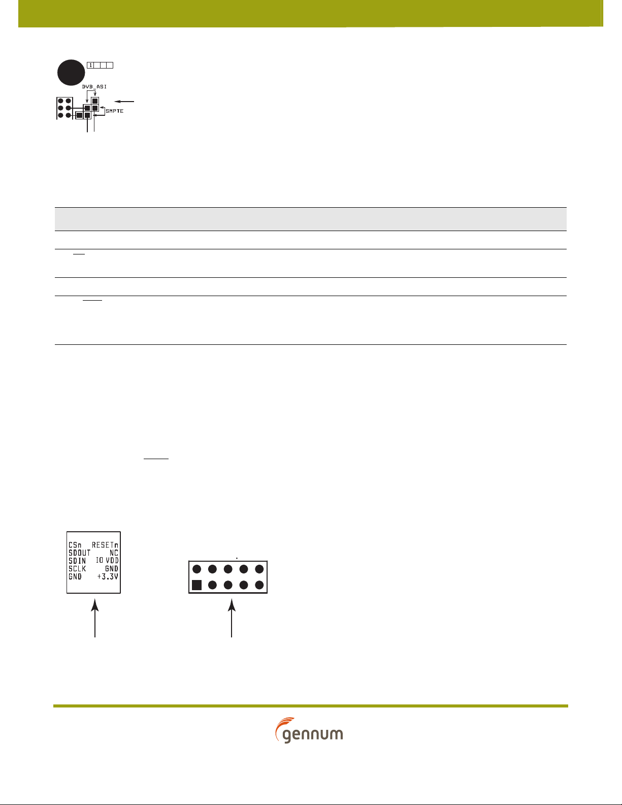
Figure 3-4: SMPTE and DVB_ASI Jumpers on the GS1572
SMPTE and DVB_ASI jumper leads.
Install two jumpers HORIZONTALLY in SMPTE mode.
Install two jumpers VERTICALLY in DVB_ASI mode.
Table 3-1: Jumper Settings
Jumper SMPTE Mode DVB-ASI Mode DATA-THROUGH Mode
DVB_ASI LOW HIGH LOW
SD/HD
SMPTE_BYPASS HIGH LOW LOW
20bit/10bit
Set HIGH to transmit SD signals.
Set LOW to transmit HD signals.
Set HIGH for 20-bit demultiplexed
input data.
Set LOW for 10-bit multiplexed
input data.
HIGH Set HIGH or LOW depending on
Switch setting ignored by device.
Input port of the GS1572 is
automatically configured for
10-bit operation.
3.5 External Control Interface
The GS1572 contains a set of internal status and configuration registers. These registers
are available to the host via the GS1572’s GSPI pins. Access to the applicable pins on the
GS1572 is provided using the JTAG/HOST interface section of the GS1572 (see
Figure 3-5).
The JTAG/HOST interface section of the GS1572 can also be used for JTAG test
operation. The JTAG/HOST
interface.
NOTE: For more information on the GS1572’s internal registers, the GSPI, or JTAG test
operation, please see the GS1572 Data Sheet.
switch is used to toggle between the JTAG and GSPI
the data rate of the input signal.
Set HIGH for 20-bit demultiplexed
input data.
Set LOW for 10-bit multiplexed
input data.
JTAG/HOST INTERFACE
1
DESCRIPTION OF
INTERFACE PINS
JTAG / HOST
INTERFACE ACCESS
Figure 3-5: JTAG/HOST Interface Block
GS1572 A Guide to Designing with the GS1572
(EB1572)
Reference Design
46282 - 1 November 2009
10 of 18
Proprietary & Confidential
Page 11
GND
GND
SCLK_TCK
C55
100N
GND
IO_VDD
1.8V 1A regulator IRU1206-18CY
3.3V 1A regulator IRU1206-33CY
VOUT
3
VIN
1
GND2GND
4
U19
IRU1206-33C Y/SOT-223
VOUT
3
VIN
1
GND2GND
4
U20
IRU1206-18C Y/SOT-223
GND
IO_VDD
1
1
2
2
3
3
4
4
J1
LP 5.00/4/90
C6
10UF
VCC
TP7
testpt
TP6
testpt
R8
NP
GND_A
C16
NP
GND
R70 0R
Reset Switch
1 2
3 4
5 6
7 8
9 10
JP2
HEADER 5X2
GND
12
C56
10U
12
C60
10U
VCC
C57
100N
VCC
DATA_IN8
DATA_IN9
C61
100N
GS1572
GS1572
PCLK
F
V
H
SDO
SDOn
DVB_ASI
SD/HD b
SMPTE_BYPASSb
RESET_TRSTb
SCLK_TCK
SDIN_TDI
CSb_TMS
SDOUT_TDO
DATA_IN[19:0]
+3.3V
+1.8V
R12 0R
GND
GND
GND_A
GND
GND_A
Input Power
DATA_IN17
DATA_IN16
DATA_IN12
DATA_IN14
DATA_IN13
DATA_IN15
DATA_IN11
DATA_IN10
DATA_IN7
DATA_IN6
DATA_IN2
DATA_IN5
DATA_IN3
DATA_IN4
GND
DATA_IN0
DATA_IN1
GND
1
3
2
J5
BNC
GND
1
TP4
1TP2 1 TP3
1 TP1
1
TP5
C86
1u
S1
B3S-1002
RESET_TRSTb
R21
2K2
GND
PCLK
C59
100N
GND
1
3
2
J3
SMA
GND
DATA_IN[19. .0]
R18 2K2
R20 2K2
R16 2K2
DVB_ASI
SD/HDb
SMPTE_BYPASSb
FEMALE
DATA_IN19
Install VERTICAL for DVB/ASI
GND
J6
Install HORIZONTAL for SMPTE
DATA_IN18
+3.3V
+3.3V
+1.8V
1 2
3 4
5 6
7 8
9 10
11 12
13 14
15 16
17 18
19 20
21 22
23 24
25 26
27 28
29 30
31 32
33 34
35 36
37 38
39 40
41 42
43 44
45 46
47 48
JP1
SQT-105-01-F-D-RA
GND
SDOUT_TDO
SDIN_TDI
+3.3V
RES ET_TR STb
2
4
6
8
10
1
3
5
7
9
JP12
HEADER 5X2
CSb_TMS
Vref_I O
GND
IO_VDD
GND
12
C45
1U
+3.3V_ CD
12
C46
1U
R26 0R
C47
10N
C44
10N
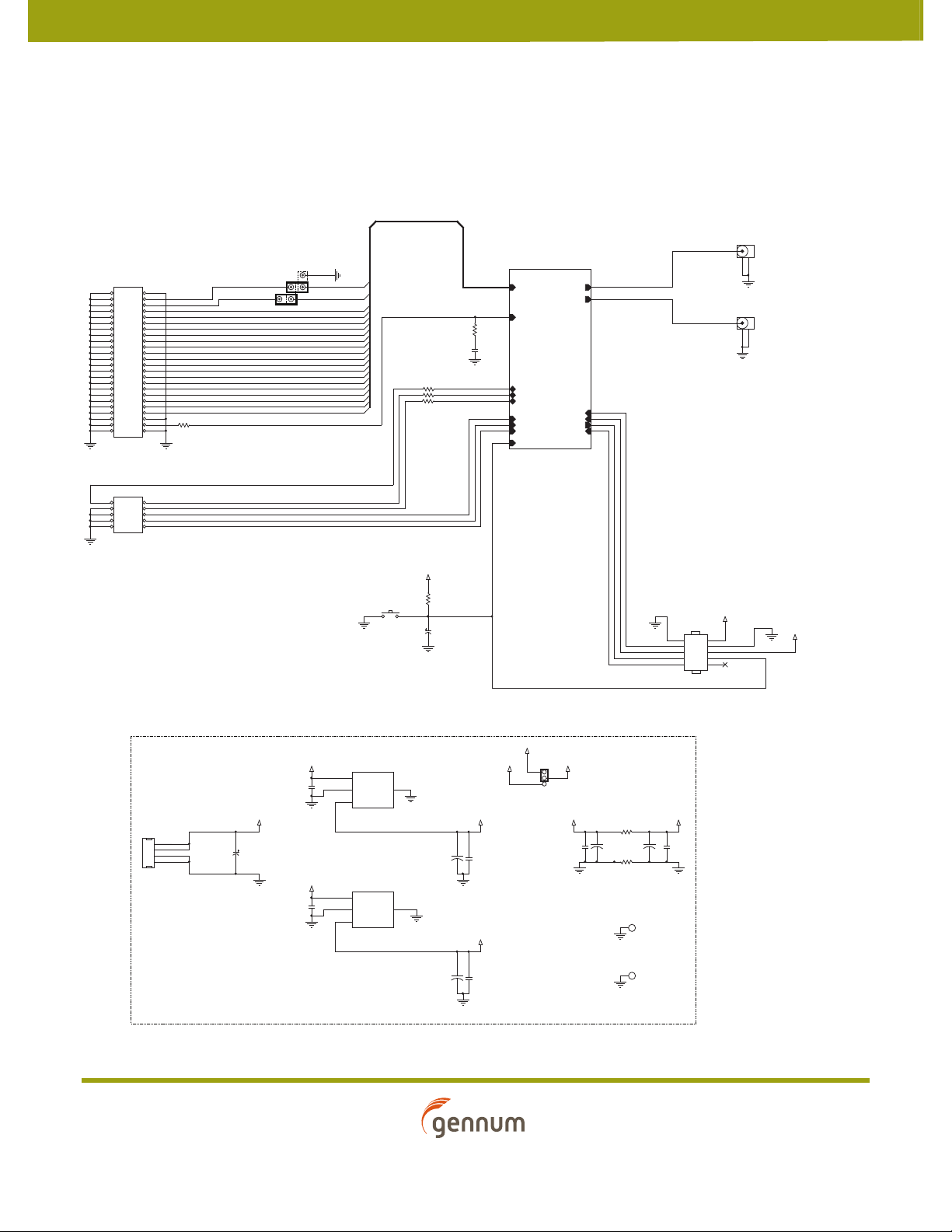
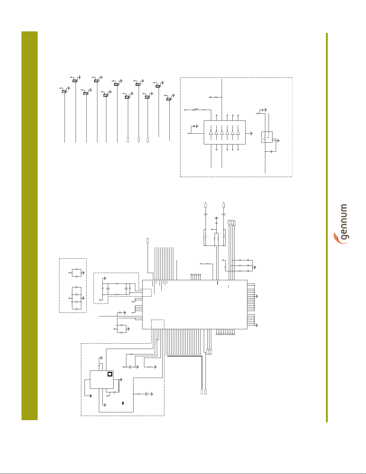
4. Board Schematic
Figure 4-1 shows the top level schematic of the GS1572. Figure 4-2 shows the chip level
in more detail.
Proprietary & Confidential
11 of 18
Figure 4-1: Top Level
GS1572 A Guide to Designing with the GS1572
(EB1572)
Reference Design
46282 - 1 November 2009
Page 12
12 of 18
DVB_ASI
GND_A
C83
10nF
SD/HDb
20bit/10bitb
IOPROC_EN/DISb
H
V
F
GND
SMPTE_BYPASSb
GND_A
GND
DETECT_TRS
SDOU T_TD O
GND
C87
10nF
GND
STANDBY_IN V
VIN
3
OUT
1
EN
4
GND
5
GND
2
U17
MIC94060
C65
10n
CABLE DRIVER POWER DOWN SWITCH (IN STANDBY MODE)
CD_VDD_SW ITCHED
GND_A
CP_RESB7VCO_VCCA8VCO_GND
B8
CORE_GND
E7
VCO
A9
TIM_86 1
G3
PCLK
B4
IO_VDD
G1
DIN18A2DIN19B3LF
A7
CP_VDD
A10
CP_GND
B10
DIN17
A1
CORE_VDD
K8
RSV
H6
DETECT_TRS
F3
CORE_GND
E6
VCO_GND
B9
DIN16
B2
CORE_VDD
G10
PD_VDD
A6
PD_VDD
B6
CORE_GND
D5
STANDBY
D3
RSVK7RSVJ7RSV
J6
DIN14C2DIN15
B1
CORE_GND
C5
CORE_GND
B5
NCD6NC
D7
DVB_ASI
G5
LOCKED
H4
RSVH5RSV
K6
DIN12C3DIN13
C1
NCD8NCE8NC
F8
SD/HD
E3
CORE_GND
E5
CORE_VDD
E1
RSV
K5
IO_VDD
H10
DIN10D2DIN11
D1
CORE_GND
F4
CORE_GND
J8
CORE_GND
G9
20BIT/10BIT
G4
CORE_GND
F5
CORE_VDD
A5
RSV
J5
IO_GND
G2
DIN8F2DIN9
F1
CORE_GND
F7
CD_GND
F9
CD_GND
E9
IOPROC_EN/ DIS
G7
SMPTE_BYPASS
G6
RESET
G8
RSV
J4
ANC_BLANK
H3
DIN6H2DIN7
H1
CD_GND
D9
CORE_GND
E2
RSV
H7
CS_TMS
K9
SCLK_TCK
J10
SDOUT_TDO
J9
RSV
K4
H/HSYNC
A4
DIN4J2DIN5
J1
CORE_GND
F6
PD_GND
C8
PD_GND
C7
PD_GND
C6
SDO_EN/DIS
D4
SDIN_TDI
K10
V/VSYNC
C4
IO_GND
H9
DIN2K2DIN3
K1
RSET
F10
CD_VDD
E10
SDO
C10
SDO
D10
CD_GND
C9
JTAG/HOST
H8
F/DE
A3
NC
E4
DIN0K3DIN1
J3
U18
GS1572
C84
10nF
+3.3V
TIM_861
GND_A
DVB_ASI
JTAG/HOSTb
H
VCO_GND
C82
10nF
C81
10nF
+1.8V
+1.8V
DATA_IN14
C67
4u7
CD_VDD_SWITCHED
PCLK
SCLK_TCK
R58
10K
SDIN_TDI
DATA_IN15
R65 75R
L2 5N 6
R60 75R
L1 5n6
1 2
C75 4u7
+1.8V
1 2
C72 4u7
R66
22k
SDO-
SDO+
R and L form the Output Return
Loss compensation Network.
SUBJECT TO CHANGE
DATA_IN16
VCO_GND
R62
75R
JTAG/HOSTb
C73
10nF
DETECT_TRS
R64 75R
DATA_IN17
ANC_BLANKb
20bit/10bitb
1 2
C63 4u7
1 2
C68 0.25p
C70 10nF
C62
0.25p
OPTIONAL TERMINATIONS
R55
0R
R54
0R
DATA_IN18
SDOn
SDO
GND
DATA_IN19
C66
10n
R69
(NP)
C78
(NP)
R68
(NP)
GND
C77
(NP)
R67
(NP)
C76
(NP)
VCO_VCC
12
C71
10u
VCO_GND
PLACE CLOSE TO GS1572.
ISOLATE WITH A MOAT ON
ALL LAYERS.
GND
R56
3R3
DATA_IN0
R57
7R
LOCKED
DATA_IN1
DATA_IN2
DATA_IN3
STANDBY
SDO_EN/DI Sb
PLACE AS CLOSE AS
POSSIBLE TO THE PINS
OF THE GS1572.
IO_VDD
DATA_IN4
DATA_IN5
VCO_GND
IOPROC_EN/ DISb
DATA_IN6
SMPTE_BYPASSb
SD/HDb
DATA_IN7
+3.3V_C D
IO_VDD
DATA_IN[19..0]
J8
GND
DATA_IN[19:0]
RESET_TRSTb
DATA_IN8
CORE_VDD, IO_VDD DECOUPLING
DATA_IN9
DVB_ASI
SD/HDb
DATA_IN10
SMPTE_BYPASSb
DATA_IN11
IO_VDD
2.5V INTERNAL ISOLATED POWER
VCO_VCC
J9
GND
IO_VDD
C88
10nF
VCTR
5
GND
4
GND
8
GND
2
VCC
7
O/P
1
NC
3
GND
6
U15
GO1555
C64
NP
12
C69
33u
VCO_GND
+3.3V_CD
R61
750R0
DATA_IN12
DATA_IN13
GND
IO_VDD
J10
GND
RESET_TRSTb
V
IO_VDD
VCO_GND
IO_VDD
GND
IO_VDD
J12
GND
IO_VDD
J13
GND
J14
GND
IO_VDD
J11
TIM_86 1
STANDBY
IO_VDD
J16
GND
IO_VDD
IO_VDD
GND
IO_VDD
CSb_TMS
J17
GND
J15
VCO_GND
+3.3V_C D
SDO_EN/DI Sb
VCO_GND
ANC_BLANKb
LOCKED
STANDBY_INV
R71
1K
1A
1
1Y
2
2A
3
2Y
4
3A
5
3Y
6
GND
7
4Y
8
4A
9
5Y
10
5A
11
6Y
12
6A
13
VCC
14
U22
74LVC04/SO
+3.3V
+3.3V
IO_VDD
C89
10nF
GND
GND
R5
500R
21
D1
LED
STANDBY
J7
SDIN_TDI
SCLK_TCK
CSb_TMS
SDOUT_TDO
C79
10nF
PCLK
F
C80
10nF
Proprietary & Confidential
Figure 4-2: Chip Level
GS1572 A Guide to Designing with the GS1572
(EB1572)
Reference Design
46282 - 1 November 2009
Page 13
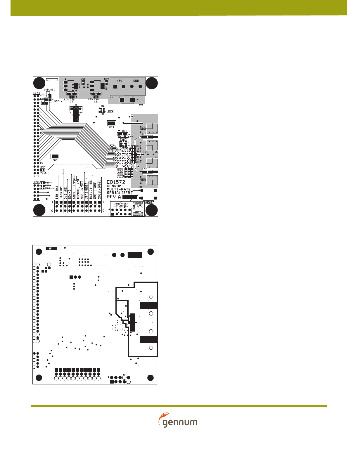
5. Board Layout
The following illustrations show the top, ground, power, and bottom layers of the
GS1572 evaluation board.
Figure 5-1: Layer 1 (Top Layer)
Figure 5-2: Layer 2 (Ground Plane, Negative Image)
GS1572 A Guide to Designing with the GS1572
(EB1572)
Reference Design
46282 - 1 November 2009
13 of 18
Proprietary & Confidential
Page 14
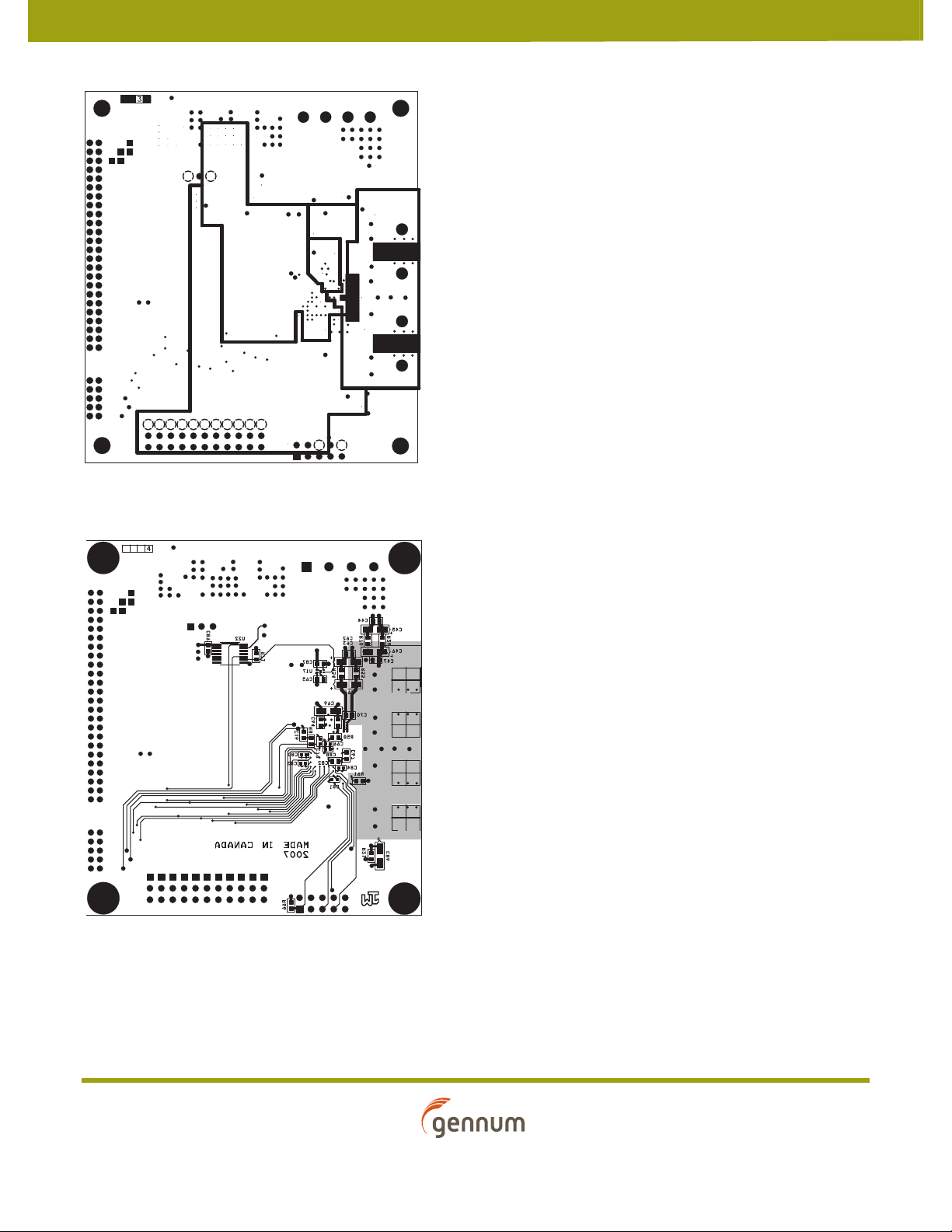
Figure 5-3: Layer 3 (Power Plane, Negative Image)
Figure 5-4: Layer 4 (Bottom Routing Layer)
GS1572 A Guide to Designing with the GS1572
(EB1572)
Reference Design
46282 - 1 November 2009
14 of 18
Proprietary & Confidential
Page 15
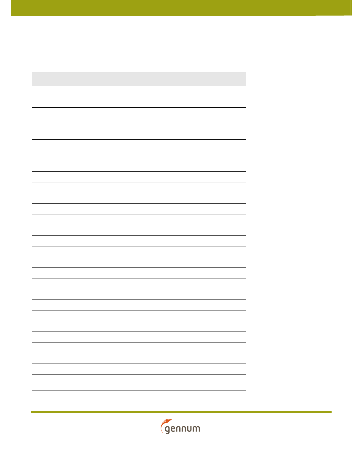
6. Bill of Materials
Table 6-1: Bill of Materials
Quantity Reference Value
1C6 10μF
2 C16, C64 (NP)
3 C44, C47, C49, C65 10nF
3 C45, C46, C86 1μF
4 C55, C57, C59, C61 100nF
3 C56, C60, C71 10μF
1 C62 0.25pF
1 C63 4.7μF
1 C66 10nF
1 C67 4.7μF
1 C68 0.25pF
1 C69 33μF
3 C70, C87, C89 10nF
2 C72, C75 4.7μF
1 C73 10nF
3 C76, C77, C78 (NP)
4 C79, C80, C83, C88 10nF
1 C81 10nF
1 C82 10nF
1 C84 10nF
1D1 LED
1 JP1 SQT-105-01-F-D-RA
1 JP2 HEADER 5X2
1 JP12 HEADER 5X2
1 J1 LP 5.00/4/90 (Power Connect)
1J3 SMA
1J5 BNC
12 J6, J7, J8, J9, J10, J11, J12, J13, J14, J15, J16,
J17
JMP_3_OPP
2 L1, L2 5n6
GS1572 A Guide to Designing with the GS1572
(EB1572)
Reference Design
46282 - 1 November 2009
15 of 18
Proprietary & Confidential
Page 16

Table 6-1: Bill of Materials (Continued)
Quantity Reference Value
1R5 500Ω
1R8 (NP)
1R12 0Ω
3 R16, R18, R20 2.2kΩ
1 R21 2.2kΩ
4 R26, R54, R55, R70 0Ω
1 R56 3.3Ω
1R57 7Ω
1 R58 10kΩ
4 R60, R62, R64, R65 75Ω
1 R61 750Ω
1 R66 22kΩ
3 R67, R68, R69 (NP)
1 R71 1kΩ
1 S1 B3S_1002
5 TP1, TP2, TP3, TP4, TP5 HEADER2MM_1_1X1 TP_0
2 TP6, TP7 Test Points
1 U15 GO1555
1 U17 MIC94060
1 U18 GS1572
1 U19 IRU1206-33CY/SOT-223
1 U20 IRU1206-18CY/SOT-223
1 U22 74LVC04/SO
GS1572 A Guide to Designing with the GS1572
(EB1572)
Reference Design
46282 - 1 November 2009
16 of 18
Proprietary & Confidential
Page 17

7. Recommended Components
Table 7-1: Recommended Components
Component Ty pe Manufacturer Notes
Resistors 1% Various Manufacturer not important. Tolerance (1%) is the only
requirement.
Capacitors TANTALUM
(LOW ESR)
Ceramic Various For values below 1uF.
Inductors 0402/0603
LQP Series
BNC
(preferred)
BNC
(alternative)
UCBBJE20-1 Trompeter
BCJ-RPC/1 Canare
NEMCO
www.nemcocaps.com
Murata
www.murata.com
www.trompeter.com
www.canare.com
Use for values of 1uF and above.
X7R and ceramic dielectric is unreliable when biased at more
than a volt. The capacitance drops to about 1/4 of its value.
X7R or NPO depending on what is available for that value.
These inductors are very well characterized. Used for return
loss matching.
End launch BNC connector for meeting return loss at 1.5Gb/s.
SD rates are less touchy. Any 75Ω will do.
End launch BNC connector for meeting return loss at 1.5Gb/s.
SD rates are less touchy. Any 75Ω will do.
GS1572 A Guide to Designing with the GS1572
(EB1572)
Reference Design
46282 - 1 November 2009
17 of 18
Proprietary & Confidential
Page 18
8. References
GS1572 Data Sheet — Multi-Rate Serializer with Cable Driver and ClockCleaner
DOCUMENT IDENTIFICATION
DATA SHEET
The product is in production. Gennum reserves the right to make changes to
the product at any time without notice to improve reliability, function or
design, in order to provide the best product possible.
GENNUM CORPORATE HEADQUARTERS
4281 Harvester Road, Burlington, Ontario L7L 5M4 Canada
OTTAWA
232 Herzberg Road, Suite 101
Kanata, Ontario K2K 2A1
Canada
Phone: +1 (613) 270-0458
Fax: +1 (613) 270-0429
CALGARY
3553 - 31st St. N.W., Suite 210
Calgary, Alberta T2L 2K7
Canada
Phone: +1 (403) 284-2672
UNITED KINGDOM
North Building, Walden Court
Parsonage Lane,
Bishop’s Stortford Hertfordshire, CM23 5DB
United Kingdom
Phone: +44 1279 714170
Fax: +44 1279 714171
INDIA
#208(A), Nirmala Plaza,
Airport Road, Forest Park Square
Bhubaneswar 751009
India
Phone: +91 (674) 653-4815
Fax: +91 (674) 259-5733
SNOWBUSH IP - A DIVISION OF GENNUM
439 University Ave. Suite 1700
Toronto, Ontario M5G 1Y8
Canada
Phone: +1 (416) 925-5643
Fax: +1 (416) 925-0581
E-mail: [email protected]
Web Site: http://www.snowbush.com
MEXICO
288-A Paseo de Maravillas
Jesus Ma., Aguascalientes
Mexico 20900
Phone: +1 (416) 848-0328
JAPAN KK
Shinjuku Green Tower Building 27F
6-14-1, Nishi Shinjuku
Shinjuku-ku, Tokyo, 160-0023
Japan
Phone: +81 (03) 3349-5501
Fax: +81 (03) 3349-5505
E-mail: [email protected]
Web Site: http://www.gennum.co.jp
TA IW A N
6F-4, No.51, Sec.2, Keelung Rd.
Sinyi District, Taipei City 11502
Taiwan R.O.C.
Phone: (886) 2-8732-8879
Fax: (886) 2-8732-8870
E-mail: [email protected]
CAUTION
ELECTROSTATIC SENSITIVE DEVICES
DO NOT OPEN PACKAGES OR HANDLE EXCEPT AT A
STATIC-FREE WORKSTATION
Phone: +1 (905) 632-2996 Fax: +1 (905) 632-2055
TM
GERMANY
Hainbuchenstraße 2
80935 Muenchen (Munich), Germany
Phone: +49-89-35831696
Fax: +49-89-35804653
E-mail: [email protected]
NORTH AMERICA WESTERN REGION
691 South Milpitas Blvd., Suite #200
Milpitas, CA 95035
United States
Phone: +1 (408) 934-1301
Fax: +1 (408) 934-1029
E-mail: [email protected]
NORTH AMERICA EASTERN REGION
4281 Harvester Road
Burlington, Ontario L7L 5M4
Canada
Phone: +1 (905) 632-2996
Fax: +1 (905) 632-2055
E-mail: [email protected]
KOREA
8F Jinnex Lakeview Bldg.
65-2, Bangidong, Songpagu
Seoul, Korea 138-828
Phone: +82-2-414-2991
Fax: +82-2-414-2998
E-mail: [email protected]
Gennum Corporation assumes no liability for any errors or omissions in this document, or for the use of the circuits or devices described herein. The sale of
the circuit or device described herein does not imply any patent license, and Gennum makes no representation that the circuit or device is free from patent
infringement.
All other trademarks mentioned are the properties of their respective owners.
GENNUM and the Gennum logo are registered trademarks of Gennum Corporation.
© Copyright 2007 Gennum Corporation. All rights reserved.
www.gennum.com
GS1572 A Guide to Designing with the GS1572
(EB1572)
Reference Design
Proprietary & Confidential
18
18 of 18
46282 - 1 November 2009
 Loading...