GENESYS GL811USB Datasheet

GL811USB -
Genesys Logic, Inc.
USB 2.0 to ATA / ATAPI Bridge
Controller
Specification 1.3
May 10, 2002
Genesys Logic, Inc.
10F, No.11, Ln.155, Sec.3, Peishen Rd., Shenkeng, Taipei, Taiwan
Tel: 886-2-2664-6655 Fax: 886-2-2664-5757
http://www.genesyslogic.com

GL811USB – USB 2.0 to ATA / ATAPI Bridge Controller
Contents
1. General Description.........................................................................................2
2. Features............................................................................................................3
3. Function Block.................................................................................................4
3.1 Block Diagram..............................................................................................4
3.2 Functional Overview.....................................................................................5
4. Pinning Information.........................................................................................7
4.1 Pin Assignment.............................................................................................7
4.2 Pin Description .............................................................................................8
5. Functional Description..................................................................................10
5.1 A TA/ ATAPI .................................................................................................10
5.2 USB 2.0......................................................................................................10
6. Electrical Characteristics..............................................................................11
6.1 Absolute Maximum Ratings........................................................................ 11
6.2 Temperature Conditions .............................................................................11
6.3 DC Characteristics...................................................................................... 11
6.4 AC Characteristics- ATA/ ATAPI..................................................................13
6.5 AC Characteristics- USB 2.0 ......................................................................33
7. Package Dimension.......................................................................................34
8. Revision History.............................................................................................35
©2000-2002 Genesys Logic Inc.—All rights reserved. Page 1

GL811USB – USB 2.0 to ATA / ATAPI Bridge Controller
1. General Description
The GL811USB is a highly-compatible, low cost USB 2.0 to ATA / ATAPI bridge
controller, which integrates Genesys Logic own design high speed UTMI (USB 2.0
Transceiver Macrocell Interface) transceiver.
As a one-chip solution which complies with Universal Serial Bus specification rev.
2.0 and ATA / ATAPI-6 specification rev 1.0, the GL811USB can support various
kinds of ATA / ATAPI device. There are totally 4 endpoints in the GL811USB
controller, Control (0), Bulk In (1), Bulk Out (2), and Interrupt (3). By complies with
the USB Storage Class specification ver.1.0 (Bulk only protocol), the GL811USB
can support not only plug and play but also Windows XP/ 2000/ ME default driver.
The GL811USB uses 12MHz crystal and slew-rate controlled pads to reduce the
EMI issue. With 48-pin LQFP (9mmX9mm) package, the GL811USB is the best
cost/ performance solution to fit different situations in the USB 2.0 high speed
storage class applications such as Hard Disk, CD-ROM, CD-R / RW and
DVD-ROM.
©2000-2002 Genesys Logic Inc.—All rights reserved. Page 2

GL811USB – USB 2.0 to ATA / ATAPI Bridge Controller
2. Features
Complies with Universal Serial Bus specification rev. 2.0.
Complies with ATA/ATAPI-6 specification rev 1.0.
Complies with USB Storage Class specification ver.1.0. (Bulk only protocol)
Operating system supported: Win XP/ 2000/ ME/ 98/ 98SE; Mac OS 9.X/ X.
Supports 4 endpoints: Control (0) / Bulk Read (1) / Bulk Write (2) / Interrupt
(3).
64 / 512 bytes Data Payload for full / high speed Bulk Endpoint.
Supports 8-bit/16-bit Standard PIO mode interface.
Supports 16-bit Multiword DMA mode and Ultra DMA mode interface (Ultra 33
/ 66 / 100).
Embedded USB 2.0 UTMI transceiver.
Embedded 7.5 MIPS RISC CPU.
ROM size: 4k words; RAM size: 128 bytes.
Supports Power Down mode and USB suspend indicator.
Supports USB 2.0 TEST mode features.
12MHz external clock to provide better EMI3.3V power input.
5V tolerance pad for IDE interface.
Supports Wakeup ability.
Available in 48-pin LQFP (9 mm * 9mm) package.
©2000-2002 Genesys Logic Inc.—All rights reserved. Page 3

C
GL811USB – USB 2.0 to ATA / ATAPI Bridge Controller
3. Function Block
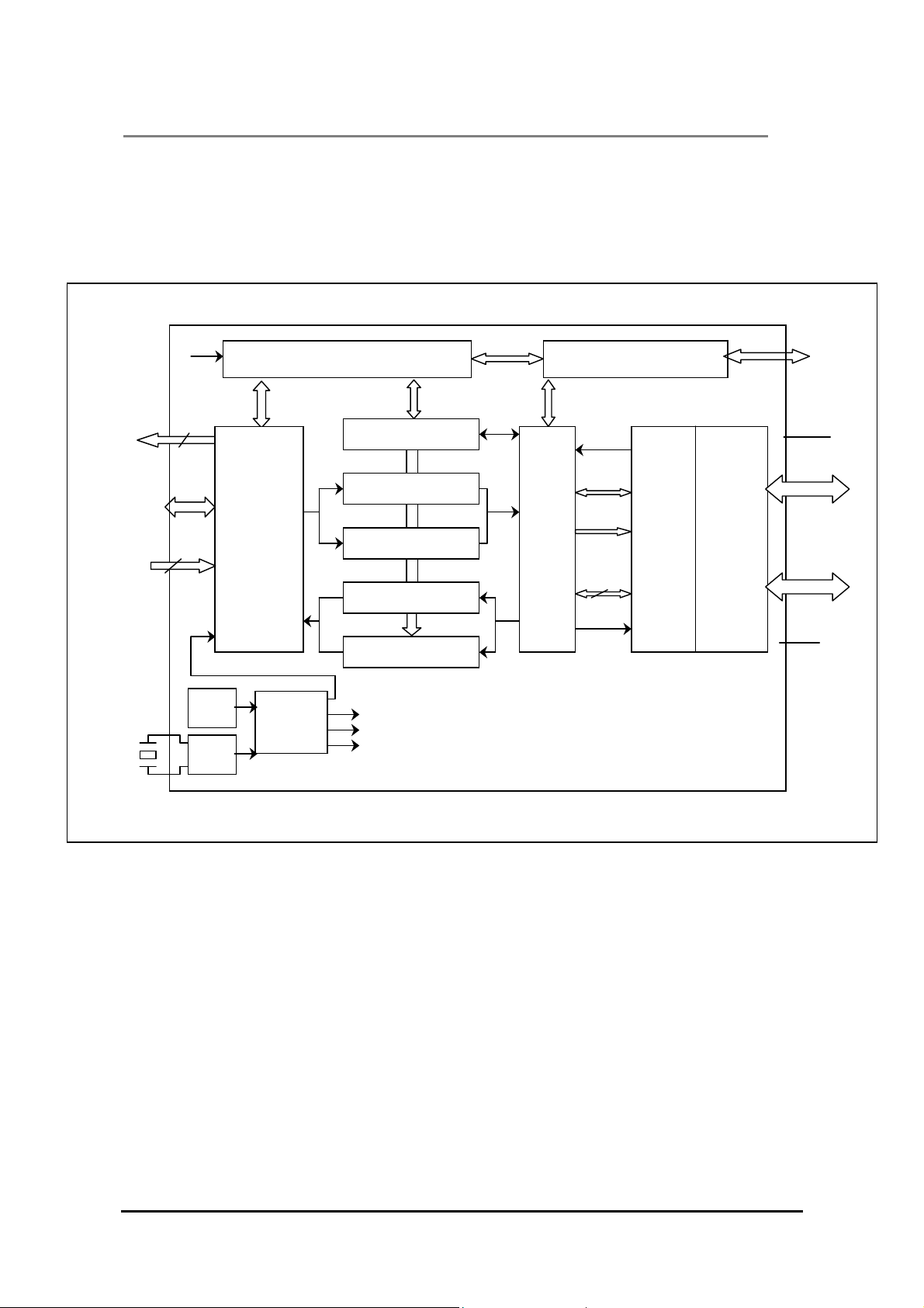
3.1 Block Diagram
DMACK_
DIOR_
DIOW_
CS1_,
CS0_
DA2
DA1
DA0
IODD15-0
INTRQ
CBLID_
DMARQ
IORDY
LK15
8
8/16-Bit
4
12-96MHz
Engine
IDE
CPU
Control Register
CLK30
RXSTS
SIE
TXCTL
16
DATA
UTMI
LOGIC
USB2.0
TXCVR
GPIO1
GPIO7
RPU
DPF
DPH
DMF
DMH
12MHz
X10
X40
RREF
Clkgen
©2000-2002 Genesys Logic Inc.—All rights reserved. Page 4

GL811USB – USB 2.0 to ATA / ATAPI Bridge Controller
3.2 Functional Overview
3.2.1 USB 2.0 TXCVR
The USB 2.0 Transceiver is the analog circuitry to handle the USB HS/FS
signaling.
3.2.2 UTMI (USB 2.0 Transceiver Macrocell Interface) Logic
The UTMI Logic is compliant to Intel’s UTMI specification 1.01. This block handles
the low level USB protocol and signaling. The major jobs of UTMI Logic is data and
clock recovery, NRZI encoding/decoding, Bit Stuffing/De-stuffing, USB2.0 test
modes supporting and serial / parallel conversion.
3.2.3 SIE (Serial Interface Engine)
The SIE contains the USB packet ID and address recognition logic, and other
sequencing and state machine logic to handle USB packets and transactions.
3.2.4 PLL
10XPLL provides the 120MHz clock output for UTMI Logic block. UTMI operates in
120MHz for USB HS data processing. 40XPLL block will provide 480MHz for USB
HS data transmission.
3.2.5 CLKGEN
CLKGEN is the clock generator block for the logic blocks. It generates 15MHz
clock for micro controller, 12MHz for PIO mode, 48MHz for MDMA mode, 96MHz
for UDMA mode, and 30MHz clock for UTMI, SIE, and FIFO.
3.2.6 CPU
The CPU is the control center of GL811USB. It’s an 8-bit micro controller operating
in 15MHz, 7.5 MIPS. After receiving a USB command, it decodes the host
command, then it re-assigns tasks to the IDE engine, GPIO, FIFO, and response
proper data/status to USB host.
3.2.7 IDE Engine
The IDE engine is extended from standard ATA / ATAPI protocol. It supports PIO
mode, multiword DMA mode, and ultra DMA mode data transfers.
©2000-2002 Genesys Logic Inc.—All rights reserved. Page 5

GL811USB – USB 2.0 to ATA / ATAPI Bridge Controller
3.2.8 FIFOs
Control FIFO is used as Control Read / Write FIFO. TXFIFO0 / TXFIFO1 are two
sets of 512-byte ping-pong FIFO for Bulk Read endpoint. It buffers data from IDE
engine, and re-direct to USB SIE logic. RXFIFO0 / RXFIFO1 are two sets of
512-byte ping-pong FIFO for Bulk Write endpoint. It buffers data from USB SIE
logic, and re-direct to IDE engine.
3.2.9 Control Registers
Control Register configures GL811USB to proper operation. For example, CPU
can set register to generate wakeup event, enter suspend, transmits proper USB
packet to host.
©2000-2002 Genesys Logic Inc.—All rights reserved. Page 6

_
A
_
K
GL811USB – USB 2.0 to ATA / ATAPI Bridge Controller
4. Pinning Information
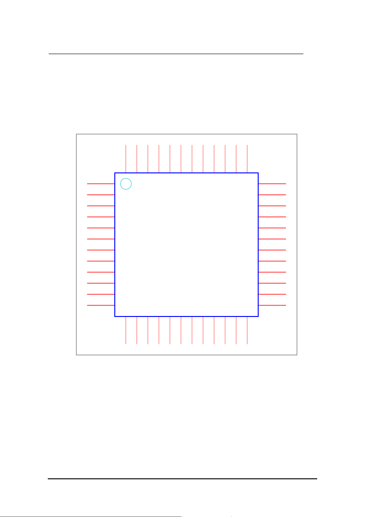
4.1 Pin Assignment
GPIO1
IODD[7]
IODD[6]
IODD[5]
IODD[4]
DVCC2
DGND2
IODD[3]
IODD[2]
IODD[1]
IODD[0]
38
23
DMARQ
37
36
35
34
33
32
31
30
29
28
27
26
25
24
DIOW_
DIOR_
IORDY
DMACK_
INTRQ
DA1
DA0
CS0_
TEST
GND1
X1
X2
IODD[10]
IODD[11]
IODD[12]
IODD[13]
IODD[14]
IODD[15]
GPIO7
IODD[8]
IODD[9]
DVCC1
DGND1
CBLID
1
2
3
4
5
6
7
8
9
10
11
12
48
47
46
45
44
43
42
41
40
39
GL811USB
48 LQFP
13
14
15
16
17
18
19
20
21
22
CS1
DA2/ S
RPU
RESET#
AVCC0
DPF
DPH
DMF
DMH
RREF
AGND0
AVCC1
©2000-2002 Genesys Logic Inc.—All rights reserved. Page 7

GL811USB – USB 2.0 to ATA / ATAPI Bridge Controller
4.2 Pin Description
Pin # Name I/O Pad Type Description Note
1
2~5
6
7
8~11
12
13
14
15
16
17
18
19
20
21
22
23
24
25
26
27
28
29
30
31
32
33
34
35
36
37
GPIO7
IODD [8:11]
DVCC1
DGND1
IODD [12:15]
CBLID_
CS1_
DA2
RESET#
RPU
AVCC0
DPF
DPH
DMF
DMH
AGND0
RREF
AVCC1
X2
X1
AGND1
TEST
CS0_
DA0
DA1
INTRQ
DMACK_
IORDY
DIOR_
DIOW_
DMARQ
B
I/O 8(*) GPIO7 (**)
B I/O 16(*) IDE data bus 8~11
tri
tri
P Power Digital VCC
P Power Digital ground
B I/O 16 IDE data bus 12~15
I I/O 8 Cable select input
O I/O 16 Chip select 1
O I/O 16 IDE address 2
I I/O 8 Reset pin (***)
tri
tri
tri
tri
pu
A U20mia 3.3v output
P Power Analog VCC
B U20mia Full speed DP
B U20mia High speed DP
B U20mia Full speed DM
B U20mia High speed DM
P Power Analog ground
A U20mia Reference resister connect (****)
P Power Analog VCC
B Clock Crystal output
I Clock Crystal input, 12Mhz
P Power Analog ground
I I/O 8 TEST mode input
O I/O 16 Chip select 0
O I/O 16 IDE address 0
O I/O 16 IDE address 1
I I/O 8 IDE interrupt input
O I/O 16 IDE acknowledge
I I/O 16 IDE ready
O I/O 16 IDE read signal
O I/O 16 IDE write signal
I I/O 8 IDE request
pd
tri
tri
tri
tri
tri
pu
tri
tri
pd
©2000-2002 Genesys Logic Inc.—All rights reserved. Page 8

4
GL811USB – USB 2.0 to ATA / ATAPI Bridge Controller
Pin # Name I/O Pad Type Description Note
38~41
42
43
4~47
48
IODD[0:3]
DGND2
DVCC2
IODD[4:7]
GPIO1
B I/O 16 IDE data bus 0~3
P Power Digital ground
P Power Digital VCC
B I/O 16 IDE data bus 4~7
B I/O 8 GPIO1
tri
tri
pd
(*) The different of I/O 8 type from I/O 16 type is the typical drive current. The typical drive
current of I/O 8 type is 8 mA, and for I/O pad 16 is 16 mA.
(**) When operating in default mode: GPIO7 is the ATA/ ATAPI reset input,
(***) When Reset pin is pulled low, the IDE bus will be in tri-state.
(****) RREF must be connected with a 510 ohm resister to ground.
Notation:
Description
Note
O Output
I Input
B Bi-directional
P Power
A Analog
pu Internal pull up
pd Internal pull down
tri Tri-state
©2000-2002 Genesys Logic Inc.—All rights reserved. Page 9

GL811USB – USB 2.0 to ATA / ATAPI Bridge Controller
5. Functional Description
5.1 ATA/ ATAPI
The GL811USB complies with ATA/ATAPI-6 specification rev. 1.0. Please refer to the
specifications for more information.
5.2 USB 2.0
The GL811USB complies with Universal Serial Bus specification rev. 2.0, and it
integrates Genesys Logic own design UTMI transceiver that fully complies with the
USB 2.0 Transceiver Macercell Interface (UTMI) specification rev. 1.01. Please refer
to the specifications for more information.
©2000-2002 Genesys Logic Inc.—All rights reserved. Page 10
 Loading...