BAL99, BAV99
Small Signal Diodes
12
.037(0.95).037(0.95)
.016 (0.4) .016 (0.4)
3
1
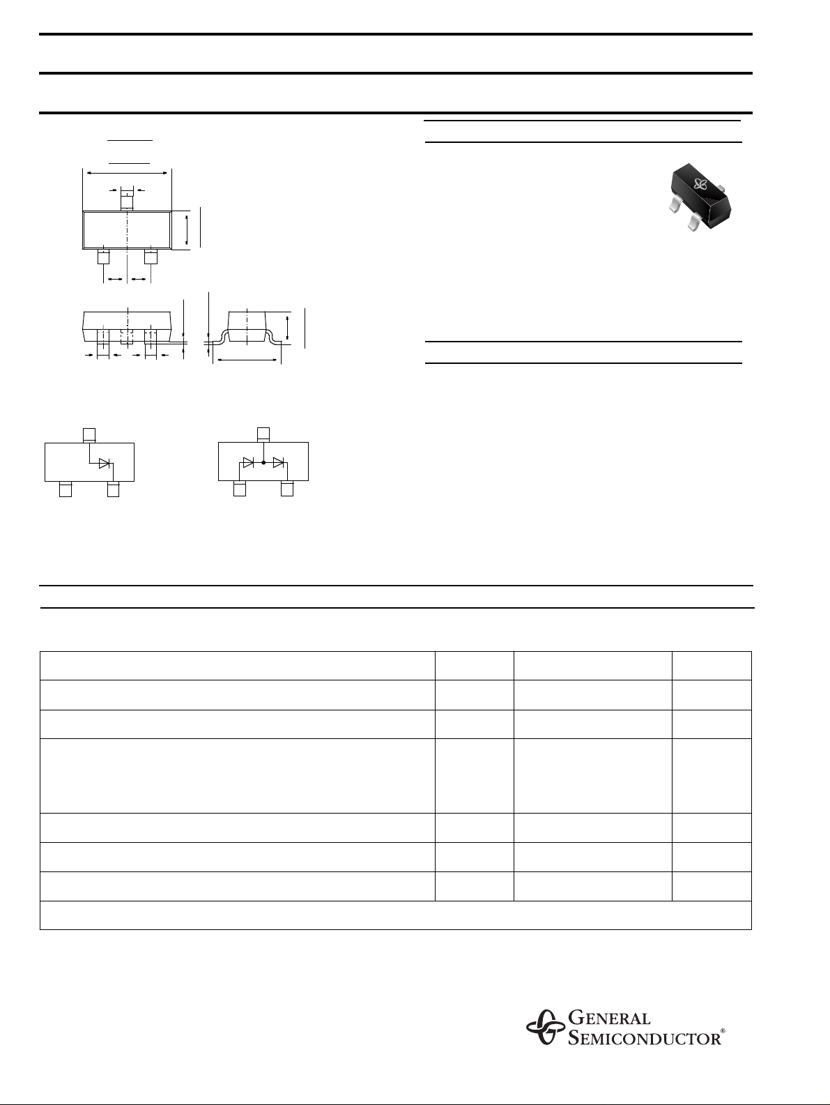
BAL99
Marking: JF
SOT-23
.122 (3.1)
.118 (3.0)
.016 (0.4)
3
Dimensions in inches and (millimeters)
Top View
)
.056 (1.43
max. .004 (0.1)
)
.052 (1.33
.007 (0.175)
.005 (0.125)
.102 (2.6)
.094 (2.4)
Top View
2
1
BAV99
Marking: JE
FEATURES
Silicon Epitaxial Planar Diode
♦
F ast s witc hing di odes, especiall y suit ed
♦
for automatic insertion.
♦
This diode is also available in other
configurations includi ng a dual common cathode with
type designation BAV70 and a dual common anode with
type designation BAW56.
.045 (1.15)
.037 (0.95)
SOT-23 Plastic Package
Case:
Weight:
3
Top View
2
MECHANICAL DATA
approx. 0.008 g
Ratings for a single diode at
Rev erse Volt age, Peak Reverse Voltage V
Forw ard Current (continuous) I
Non-Repetitive Peak Forward Current
at t = 1 µs
at t = 1 ms
at t = 1 s
Power Dissipation at T
Junction Temperature T
Storage Temperature Range T
1)
Device on fiberglas s subs tr at e, see layout.
ambient temperature unless otherwise specified.
25 °C
= 25 °C P
amb
MAXIMUM RATINGS AND ELECTRICAL CHARACTERISTICS
Symbol Value Unit
R, VRM
F
I
FSM
I
FSM
I
FSM
tot
j
S
70 V
250 mA
2
1
0.5
350
1)
A
A
A
mW
150 °C
–65 to +150 °C
4/98

Ratings for one diode at
Forw ard Voltage
at I
= 1 mA
F
= 10 mA
at I
F
= 50 mA
at I
F
= 150 mA
at I
F
Leakage Current
= 70 V
at V
R
at V
= 70 V, Tj = 150 °C
R
= 25 V, Tj = 150 °C
at V
R
BAL99, BAV99
ELECTRICAL CHARACTERISTICS
ambient temperature unless otherwise specified
25 °C
Symbol Min. Ty p. Max. Unit
V
F
V
F
V
F
V
F
I
R
I
R
I
R
–
–
–
–
–
–
–
–
–
–
–
–
–
–
0.715
0.855
1.0
1.25
2.5
100
30
V
V
V
V
µ
A
µ
A
µ
A
Capacitance
= VR = 0; f = 1 MHz
at V
F
Rev erse Recovery Time
= 10 mA to IR = 10 mA
from I
F
measured at I
= 1 mA, RL = 100
R
Ω
Thermal Resistance
Junction to Ambient Air
1)
Device on fiberg lass subs tr ate, see layout.
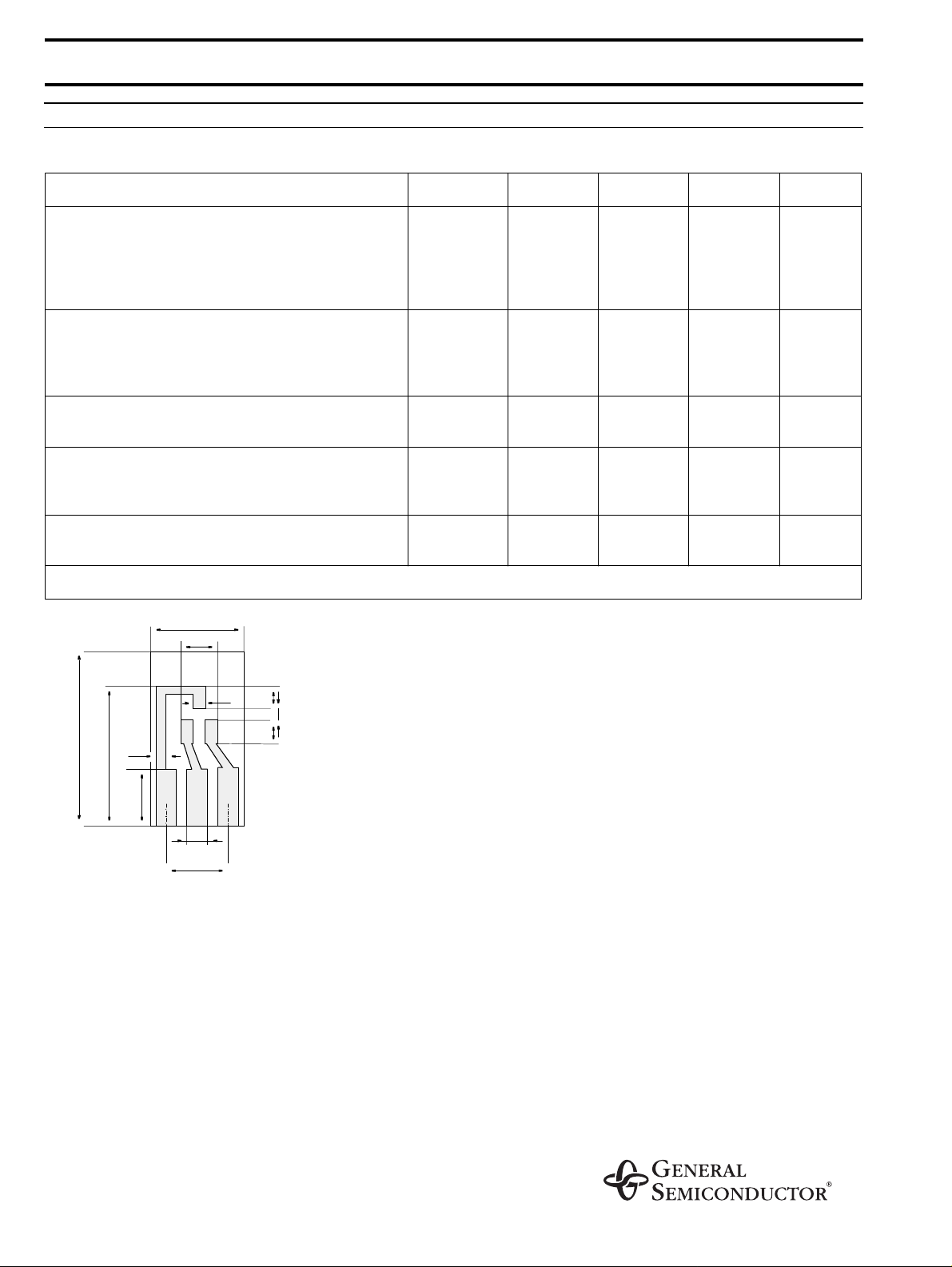
.30 (7.5)
.12 (3)
.04 (1)
.08 (2)
.04 (1)
.59 (1 5)
.03 (0.8)
.47 (1 2)
0.2 (5)
.06 (1.5)
.20 (5.1)
.08 (2)
Dim ensions in inches (mil limete r s)
C
t
R
rr
tot
thJA
––1.5pF
––6ns
– – 430
1)
K/W
Layout fo r R
thJA
test
Thickness: Fiberglass 0.059 in (1.5 mm)
Copper leads 0.012 in (0.3 mm)

 Loading...