

P6KE6.8 THRU P6KE440CA
TRANSZORB™ TRANSIENT VOLTAGE SUPPRESSOR
Breakdown Voltage - 6.8 to 440 Volts Peak Pulse Power- 600 Watts
FEATURES
♦ Plastic package has Underwriters Laboratory
Flammability Classification 94V-0
♦ Glass passivated junction
♦ 600W peak pulse power capability with a 10/1000µs
waveform, repetition rate (duty cycle): 0.01%
♦ Excellent clamping
capability
♦ Low incremental surge resistance
♦ Fast response time: typically less
than 1.0ps from 0 Volts to V
(BR)
for
uni-directional and 5.0ns for bi-directional types
♦ Typical IDless than 1µA above 10V
♦ High temperature soldering guaranteed:
265°C/10 seconds, 0.375" (9.5mm) lead length,
5lbs. (2.3 kg) tension
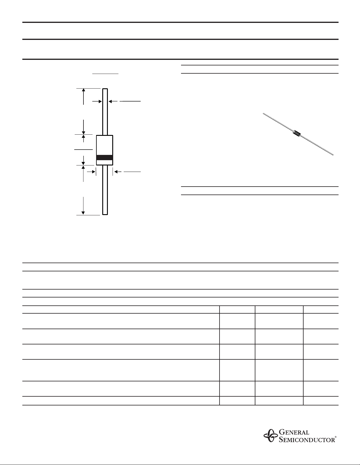
MECHANICAL DATA
Case: JEDEC DO-204AC molded plastic body over
passivated junction
Terminals: Solder plated axial leads, solderable per
MIL-STD-750, Method 2026
Polarity: For uni-directional types the color band denotes
the cathode, which is postitive with respect to the anode
under normal TVS operation
Mounting Position: Any
Weight: 0.015 ounce, 0.4 gram
DEVICES FOR BIDIRECTIONAL APPLICATIONS
For bi-directional use C or CA Suffix for types P6KE6.8 thru types P6KE440 (e.g. P6KE6.8C, P6KE440CA).
Electrical characteristics apply in both directions.
MAXIMUM RATINGS AND CHARACTERISTICS
Ratings at 25°C ambient temperature unless otherwise specified.
SYMBOL VALUE UNITS
Peak pulse power dissipation with a 10/1000µs
waveform
(NOTE 1, FIG. 1)
P
PPM
Minimum 600 Watts
Peak pulse current with a 10/1000µs waveform
(NOTE 1)
I
PPM SEE TABLE 1
Amps
Steady state power dissipation at T
L
=75°C
lead lengths, 0.375" (9.5mm)
(NOTE 2)
P
M(AV)
5.0 Watts
Peak forward surge current, 8.3ms single half
sine-wave superimposed on rated load
(JEDEC Method) unidirectional only
(NOTE 3)
I
FSM
100.0 Amps
Maximum instantaneous forward voltage at 50.0A for
unidirectional only
(NOTE 4)
V
F
3.5/5.0 Volts
Operating junction and storage temperature range TJ, T
STG
-55 to +175 °C
NOTES:
(1) Non-repetitive current pulse, per Fig. 3 and derated above T
A
=25°C per Fig. 2
(2) Mounted on copper pad area of 1.6 x 1.6” (40 x 40mm) per Fig. 5
(3) Measured on 8.3ms single half sine-wave or equivalent square wave duty cycle=4 pulses per minute maximum
(4) V
F
=3.5 Volt max. for devices of V
(BR)
≤220V, and VF=5.0V for devices of V
(BR)
>220V
1/21/99
DO-204AC
Dimensions in inches
and
(millimeters)
1.0
(25.4)
MIN.
0.300 (7.6)
0.230 (5.8)
1.0
(25.4)
MIN.
0.034 (0.86)
0.028 (0.71)
DIA.
0.140 (3.6)
0.104 (2.6)
DIA.

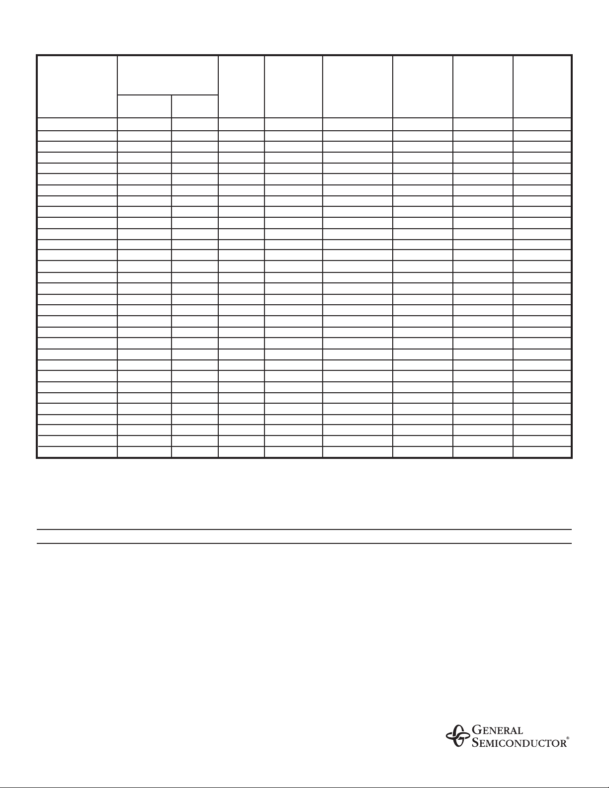
ELECTRICAL CHARACTERISTICS at (T
A
=25°C unless otherwise noted) TABLE 1
Maximum
Breakdown Voltage Maximum Peak Pulse Maximum Maximum
V
(BR)
Reverse Current Clamping Temperature
Volts
(NOTE 1)
Test Stand-off Leakage I
PPM
Voltage at Coefficient
Current Voltage at V
WM
I
PPM
of V
(BR)
Device Type MIN MAX
at I
T
V
WM
ID (µA) (Amps) VC (Volts) (% / C)
(mA)
(Volts)
(NOTE3) (NOTE 2)
+P6KE6.8 6.12 7.48 10 5.50 1000 55.6 10.8 0.057
+P6KE6.8A 6.45 7.14 10 5.80 1000 57.1 10.5 0.057
+P6KE7.5 6.75 8.25 10 6.05 500 51.3 11.7 0.061
+P6KE7.5A 7.13 7.88 10 6.40 500 53.1 11.3 0.061
+P6KE8.2 7.38 9.02 10 6.63 200 48.0 12.5 0.065
+P6KE8.2A 7.79 8.61 10 7.02 200 49.6 12.1 0.065
+P6KE9.1 8.19 10.0 1.0 7.37 50 43.5 13.8 0.068
+P6KE9.1A 8.65 9.55 1.0 7.78 50 44.8 13.4 0.068
+P6KE10 9.00 11.0 1.0 8.10 10 40.0 15.0 0.073
+P6KE10A 9.50 10.5 1.0 8.55 10 41.4 14.5 0.073
+P6KE11 9.90 12.1 1.0 8.92 5.0 37.0 16.2 0.075
+P6KE11A 10.5 11.6 1.0 9.40 5.0 38.5 15.6 0.075
+P6KE12 10.8 13.2 1.0 9.72 5.0 34.7 17.3 0.078
+P6KE12A 11.4 12.6 1.0 10.2 5.0 35.9 16.7 0.078
+P6KE13 11.7 14.3 1.0 10.5 5.0 31.6 19.0 0.081
+P6KE13A 12.4 13.7 1.0 11.1 5.0 33.0 18.2 0.081
+P6KE15 13.5 16.5 1.0 12.1 5.0 27.3 22.0 0.084
+P6KE15A 14.3 15.8 1.0 12.8 5.0 28.3 21.2 0.084
+P6KE16 14.4 17.6 1.0 12.9 5.0 25.5 23.5 0.086
+P6KE16A 15.2 16.8 1.0 13.6 5.0 26.7 22.5 0.086
+P6KE18 16.2 19.8 1.0 14.5 5.0 22.6 26.5 0.088
+P6KE18A 17.1 18.9 1.0 15.3 5.0 23.8 25.2 0.088
+P6KE20 18.0 22.0 1.0 16.2 5.0 20.6 29.1 0.090
+P6KE20A 19.0 21.0 1.0 17.1 5.0 21.7 27.7 0.090
+P6KE22 19.8 24.2 1.0 17.8 5.0 18.8 31.9 0.092
+P6KE22A 20.9 23.1 1.0 18.8 5.0 19.6 30.6 0.092
+P6KE24 21.6 26.4 1.0 19.4 5.0 17.3 34.7 0.094
+P6KE24A 22.8 25.2 1.0 20.5 5.0 18.1 33.2 0.094
+P6KE27 24.3 29.7 1.0 21.8 5.0 15.3 39.1 0.096
+P6KE27A 25.7 28.4 1.0 23.1 5.0 16.0 37.5 0.096
+P6KE30 27.0 33.0 1.0 24.3 5.0 13.8 43.5 0.097
+P6KE30A 28.5 31.5 1.0 25.6 5.0 14.5 41.4 0.097
+P6KE33 29.7 36.3 1.0 26.8 5.0 12.6 47.7 0.098
+P6KE33A 31.4 34.7 1.0 28.2 5.0 13.1 45.7 0.098
+P6KE36 32.4 39.6 1.0 29.1 5.0 11.5 52.0 0.099
+P6KE36A 34.2 37.8 1.0 30.8 5.0 12.0 49.9 0.099
+P6KE39 35.1 42.9 1.0 31.6 5.0 10.6 56.4 0.100
+P6KE39A 37.1 41.0 1.0 33.3 5.0 11.1 53.9 0.100
+P6KE43 38.7 47.3 1.0 34.8 5.0 9.7 61.9 0.101
+P6KE43A 40.9 45.2 1.0 36.8 5.0 10.1 59.3 0.101
+P6KE47 42.3 51.7 1.0 38.1 5.0 8.8 67.8 0.101
+P6KE47A 44.7 49.4 1.0 40.2 5.0 9.3 64.8 0.101
P6KE51 45.9 56.1 1.0 41.3 5.0 8.2 73.5 0.102
P6KE51A 48.5 53.6 1.0 43.6 5.0 8.6 70.1 0.102
P6KE56 50.4 61.6 1.0 45.4 5.0 7.5 80.5 0.103
P6KE56A 53.2 58.8 1.0 47.8 5.0 7.8 77.0 0.103
P6KE62 55.8 68.2 1.0 50.2 5.0 6.7 89.0 0.104
P6KE62A 58.9 65.1 1.0 53.0 5.0 7.1 85.0 0.104
P6KE68 61.2 74.8 1.0 55.1 5.0 6.1 98.0 0.104
P6KE68A 64.6 71.4 1.0 58.1 5.0 6.5 92.0 0.104
P6KE75 67.5 82.5 1.0 60.7 5.0 5.6 108 0.105
P6KE75A 71.3 78.8 1.0 64.1 5.0 5.8 103 0.105
P6KE82 73.8 90.2 1.0 66.4 5.0 5.1 118 0.105
P6KE82A 77.9 86.1 1.0 70.1 5.0 5.3 113 0.105
P6KE91 81.9 100 1.0 73.7 5.0 4.6 131 0.106
+UL listed for Telecom application protection 497B, file number E136766 for both uni-directional and bi-directional devices
ELECTRICAL CHARACTERISTICS at (T
A
=25°C unless otherwise noted) TABLE (Cont’d)
Maximum
Breakdown Voltage Maximum Peak Pulse Maximum Maximum
V
(BR)
Reverse Current Clamping Temperature
Volts
(NOTE 1)
Test Stand-off Leakage I
PPM
Voltage at Coefficient
Current Voltage at V
WM
I
PPM
of V
(BR)
Device Type MIN MAX
at I
T
V
WM
ID (µA) (Amps) VC (Volts) (% / C)
(mA)
(Volts)
(NOTE3) (NOTE 2)
P6KE91A 86.5 95.5 1.0 77.8 5.0 4.8 125 0.106
P6KE100 90.0 110 1.0 81.0 5.0 4.2 144 0.106
P6KE100A 95.0 105 1.0 85.5 5.0 4.4 137 0.106
P6KE110 99.0 121 1.0 89.2 5.0 3.8 158 0.107
P6KE110A 105 116 1.0 94.0 5.0 3.9 152 0.107
P6KE120 108 132 1.0 97.2 5.0 3.5 173 0.107
P6KE120A 114 126 1.0 102 5.0 3.6 165 0.107
P6KE130 117 143 1.0 105 5.0 3.2 187 0.107
P6KE130A 124 137 1.0 111 5.0 3.4 179 0.107
P6KE150 135 165 1.0 121 5.0 2.8 215 0.108
P6KE150A 143 158 1.0 128 5.0 2.9 207 0.108
P6KE160 144 176 1.0 130 5.0 2.6 230 0.108
P6KE160A 152 168 1.0 136 5.0 2.7 219 0.108
P6KE170 153 187 1.0 138 5.0 2.5 244 0.108
P6KE170A 162 179 1.0 145 5.0 2.6 234 0.108
P6KE180 162 198 1.0 146 5.0 2.3 258 0.108
P6KE180A 171 189 1.0 154 5.0 2.4 246 0.108
P6KE200 180 220 1.0 162 5.0 2.1 287 0.108
P6KE200A 190 210 1.0 171 5.0 2.2 274 0.108
P6KE220 198 242 1.0 175 5.0 1.7 344 0.108
P6KE220A 209 231 1.0 185 5.0 1.8 328 0.108
P6KE250 225 275 1.0 202 5.0 1.7 360 0.110
P6KE250A 237 263 1.0 214 5.0 1.7 344 0.110
P6KE300 270 330 1.0 243 5.0 1.4 430 0.110
P6KE300A 285 315 1.0 256 5.0 1.4 414 0.110
P6KE350 315 385 1.0 284 5.0 1.2 504 0.110
P6KE350A 333 368 1.0 300 5.0 1.2 482 0.110
P6KE400 360 440 1.0 324 5.0 1.0 574 0.110
P6KE400A 380 420 1.0 342 5.0 1.1 548 0.110
P6KE440 396 484 1.0 356 5.0 0.95 631 0.110
P6KE440A 418 462 1.0 376 5.0 1.0 602 0.110
NOTES:
(1) V
(BR)
measured after ITapplied for 300µs, IT=square wave pulse or equivalent
(2) Surge current waveform per Fig. 3 and derate per Fig. 2
(3) For bidirectional types with V
WM
of 10 volts and less, the IDlimit is doubled
(4) All terms and symbols are consistent with ANSI/IEEE C62.35
+UL listed for Telecom application protection 497B, file number E136766 for both uni-directional and bi-directional devices
DESCRIPTION
This P6KE TVS series is a low cost commercial product for use in applications where large voltage transients can permanently
damage voltage-sensitive components.
The P6KE series device types are designed in a small package size where power and space is a consideration. They are characterized by their high surge capability, extremely fast response time, and low impedance, (Ron). Because of the unpredictable nature of
transients, and the variation of the impedance with respect to these transients, impedance, per se, is not specified as a parametric
value. However, a minimum voltage at low current conditions (BV) and a maximum clamping voltage (Vc) at a maximum peak pulse
current is specified.
In some instances, the thermal effect (see Vc Clamping Voltage) may be responsible for 50% to 70%. of the observed voltage differential when subjected to high current pulses for several duty cycles, thus making a maximum impedance specification insignificant.
In case of a severe current overload or abnormal transient beyond the maximum ratings, the Transient Voltage Suppressor will initially
fail 'short' thus tripping the system's circuit breaker or fuse while protecting the entire circuit. Curves depicting clamping voltage vs.
various current pulses are available from the factory. Extended power curves vs. pulse time are also available.

RATINGS AND CHARACTERISTIC CURVES P6KE6.8 THRU P6KE440CA
FIG. 1 - PEAK PULSE POWER RATING CURVE
P
PPM
, PEAK PULSE POWER, kW
td, PULSE WIDTH, sec.
TA, AMBIENT TEMPERATURE, °C
FIG. 4 - TYPICAL JUNCTION CAPACITANCE
UNIDIRECTIONAL
FIG. 3 - PULSE WAVEFORM
t, TIME, ms
V
(BR)
, BREAKDOWN VOLTAGE, VOLTS
TL,LEAD TEMPERATURE,°C
V
(BR),
BREAKDOWN VOLTAGE, VOLTS
NUMBER OF CYCLES AT 60 H
Z
I
PPM,
PEAK PULSE CURRENT, %
PEAK PULSE POWER (P
PP
) or CURRENT (I
PP
)
DERATING IN PERCENTAGE, %
C
J
, JUNCTION CAPACITANCE, pF
I
FSM
, PEAK FORWARD SURGE CURRENT,
AMPERES
NON-REPETITIVE
PULSE WAVEFORM
SHOWN in FIG. 3 TA=25°C
PULSE WIDTH (td) is DEFINED
as the POINT WHERE the PEAK
CURRENT DECAYS to 50% of I
PP
tr=10µsec.
TJ=25°C
f=1 MHz
Vsig=50mVp-p
MEASURED at
ZERO BIAS
MEASURED at
STAND-OFF
VOLTAGE V
WM
TA=25°C
MEASURED at
DEVICES
STAND-OFF
VOLTAGE, V
WM
1.6 x 1.6 x 0.040”
(40 x 40 x 1mm.)
COPPER HEAT SINKS
60 HZ
RESISTIVE OR
INDUCTIVE LOAD
8.3ms SINGLE HALF SINE-WAVE
(JEDEC Method)
td
PEAK VALUE
I
PPM
HALF VALUE - I
PP
2
10/1000µsec. WAVEFORM
as DEFINED by R.E.A.
FIG. 6 - MAXIMUM NON-REPETITIVE FORWARD
SURGE CURRENT UNI-DIRECTIONAL
FIG. 5 - STEADY STATE POWER DERATING CURVE
PM
(AV),
STEADY STATE POWER DISSIPATION,
WATTS
I
D,
INSTANTANEOUS REVERSE LEAKAGE
CURRENT, MICROAMPERES
FIG. 2 - PULSE DERATING CURVE
FIG. 7- TYPICAL REVERSE LEAKAGE CHARACTERISTICS
= 0.375” (9.5mm.)
LEAD LENGTHS
L
100
10
1.0
0.1
0.1
µ
s
1.0
µ
s
150
100
50
0
0
1.0
5.0
3.75
2.5
1.25
0
0 25 50 75 100 125 150 175 200
1,000
100
10
1
0.1
10
µ
s
100
µ
s
2.0
3.0
1.0ms 10ms
4.0
100
75
50
25
0
25
0
50
6,000
1,000
100
10
1
200
100
50
10
1
100
125
150
75
10
100 200
10
175
200
100
0.01
0.001
0
100
200
300
400
440
500
 Loading...