General Semiconductor BF820, BF822 Datasheet

BF820, BF822
Small Signal Transistors (NPN)
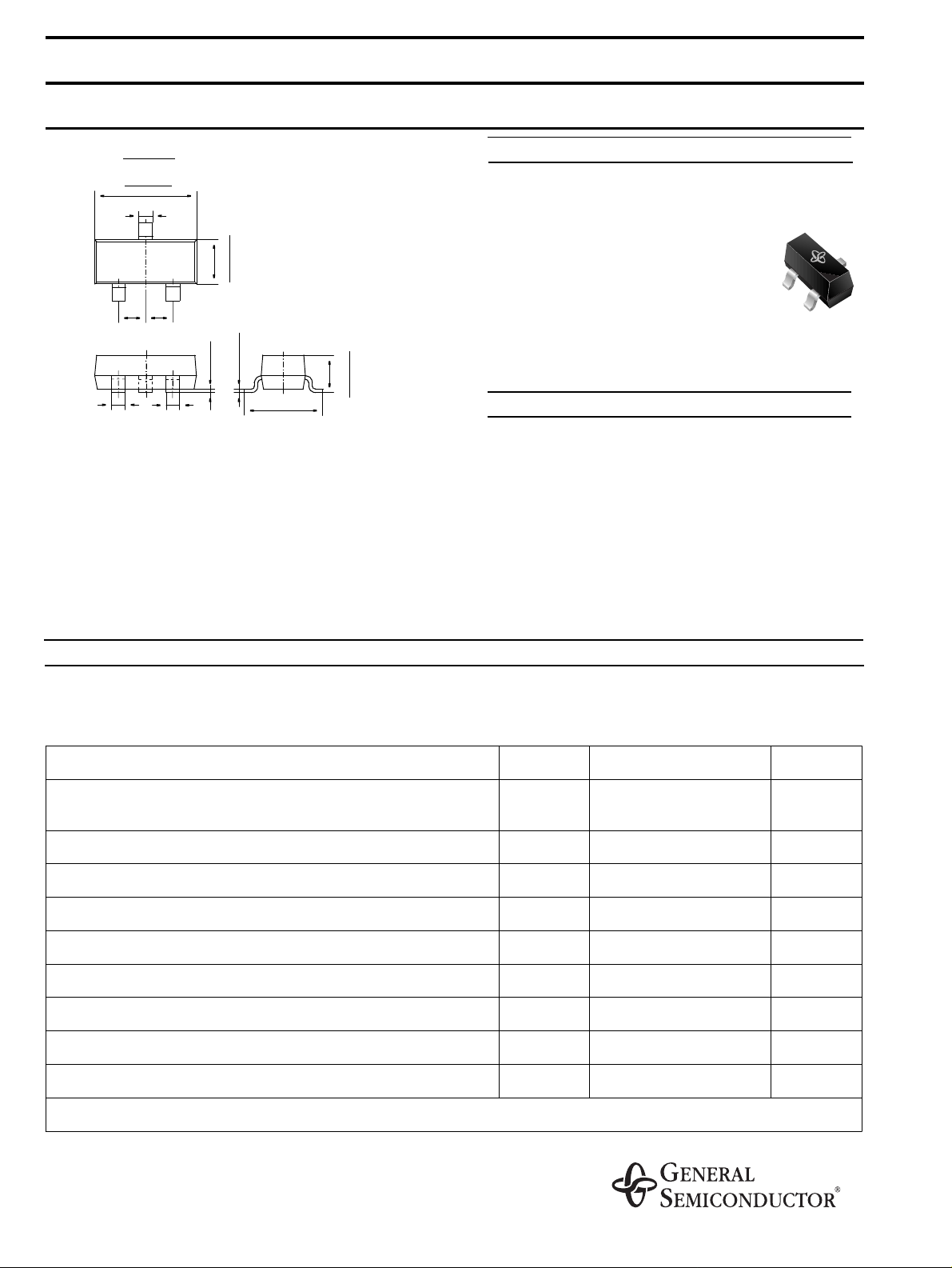
SOT-23
.122 (3.1)
.118 (3.0)
.016 (0.4)
3
12
.037(0.95).037(0.95)
.016 (0.4) .016 (0.4)
Dimensions in inches and (millimeters)
Pin configur ation
1 = Base, 2 = Emitter, 3 = Collector.
Top View
)
.056 (1.43
max. .004 (0.1)
)
.052 (1.33
.007 (0.175)
.005 (0.125)
.102 (2.6)
.094 (2.4)
.045 (1.15)
FEATURES
♦
NPN Silicon Epitaxial Planar Transistors
especially suited for applicat i on in class-B
video output stages of TV receivers and
monitors.
As complementary types, the PNP tran-
♦
sistors BF821 and BF823 are recommended.
.037 (0.95)
SOT-23 Plastic Package
Case:
Weight:
Marking code
BF820 = 1V
BF822 = 1X
MECHANICAL DATA
approx. 0.008 g
MAXIMUM RATINGS AND ELECTRICAL CHARACTERISTICS
Ratings at
Collector-Base Voltage BF820
Collector-Emitter Voltage BF822 V
Collector-Emitter Voltage BF820 V
Emitter-Base Voltage V
Collector Current I
Peak Collector Current I
Power Dissipation at T
Junction Temperature T
Storage Temperature Range T
1)
Device on fiberglass substrate, see layout
ambient temperature unless otherwise specified
25 °C
= 50 °C P
SB
BF822
Symbol Value Unit
V
V
C
CM
CBO
CBO
CEO
CER
EBO
tot
j
S
300
250
250 V
300 V
5V
50 mA
100 mA
1)
300
150 °C
– 65 to +150 °C
V
V
mW
4/98

Ratings at
ambient temperature unless otherwise specified
25 °C
BF820, BF822
ELECTRICAL CHARACTERISTICS
Symbol Min. Typ. Max. Unit
Collector-Base Brea kdown Voltage BF820
at I
= 100 µA, IB = 0 BF822
C
Collector-Emitter Breakdown Voltage BF822
= 10 mA, IE = 0
at I
C
Collector-Emitter Breakdown Voltage BF820
at R
= 2.7 kΩ, IC = 10 mA
BE
Emitter-Base Breakdown Voltage
= 100 µA, IB = 0
at I
E
Collector-Base Cutoff Current
= 200 V, IE = 0
at V
CB
Collector-Em i tter Cutoff Current
= 2.7 kΩ, VCE = 250 V
at R
BE
= 2.7 kΩ, VCE = 200 V, Tj = 150 °C
at R
BE
Collector Saturation Voltage
= 30 mA, IB = 5 mA
at I
C
DC Current Gain
= 20 V, IC = 25 mA
at V
CE
Gain-Bandwidth Product
= 10 V, IC = 10 mA
at V
CE
V
(BR)CBO
V
(BR)CBO
V
(BR)CEO
V
(BR)CER
V
(BR)EBO
I
CBO
I
CER
I
CER
V
CEsat
h
FE
f
T
300
250
–
–
–
–
V
V
250 – – V
300––V
5––V
––10nA
50
10
nA
µ
A
––0.6V
50–––
60––MHz
Feedback Capacitance
= 30 V, IC = 0, f = 1 MHz
at V
CE
Thermal Resistance Junction to Ambient Air R
1)
Device on fiber glass sub st rate, see layout
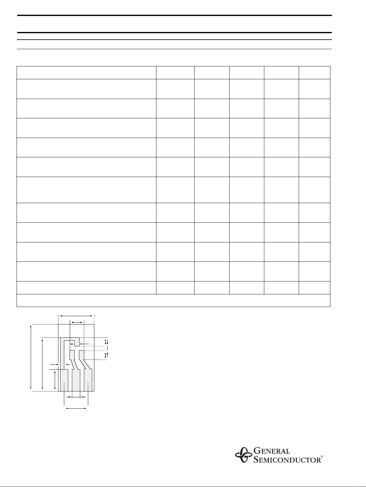
.30 ( 7.5)
.12 ( 3)
.04 (1)
.08 (2)
.04 ( 1)
.59 (1 5)
.03 ( 0.8)
.47 (1 2)
0.2 (5)
Layout fo r R
thJA
.06 (1.5)
.20 ( 5.1)
test
.08 (2)
Dim ensions in inches (millimeters)
Thickness: Fiberglass 0.059 in (1.5 mm)
Copper leads 0.012 in (0.3 mm)
C
re
thJA
––1.6pF
– – 430
1)
K/W
 Loading...