

Page 1
GE
Data Sheet
April 24, 2013
©2012 General Electric Company. All rights reserved.
Page 1
Features
Compliant to RoHS EU Directive 2002/95/EC (Z versions)
Compatible in a Pb-free or SnPb reflow environment (Z
versions)
Compliant to IPC-9592 (September 2008), Category 2, Class II
DOSA based
Wide Input voltage range (3Vdc-14.4Vdc)
Output voltage programmable from 0.45Vdc to 5.5Vdc via
external resistor and PMBus
TM #
Digital interface through the PMBus
TM #
protocol
Tunable Loop
TM
to optimize dynamic output voltage response
Flexible output voltage sequencing EZ-SEQUENCE
Power Good signal
Fixed switching frequency with capability of external
synchronization
Output over current protection (non-latching)
Over temperature protection
Remote On/Off
Ability to sink and source current
Cost efficient open frame design
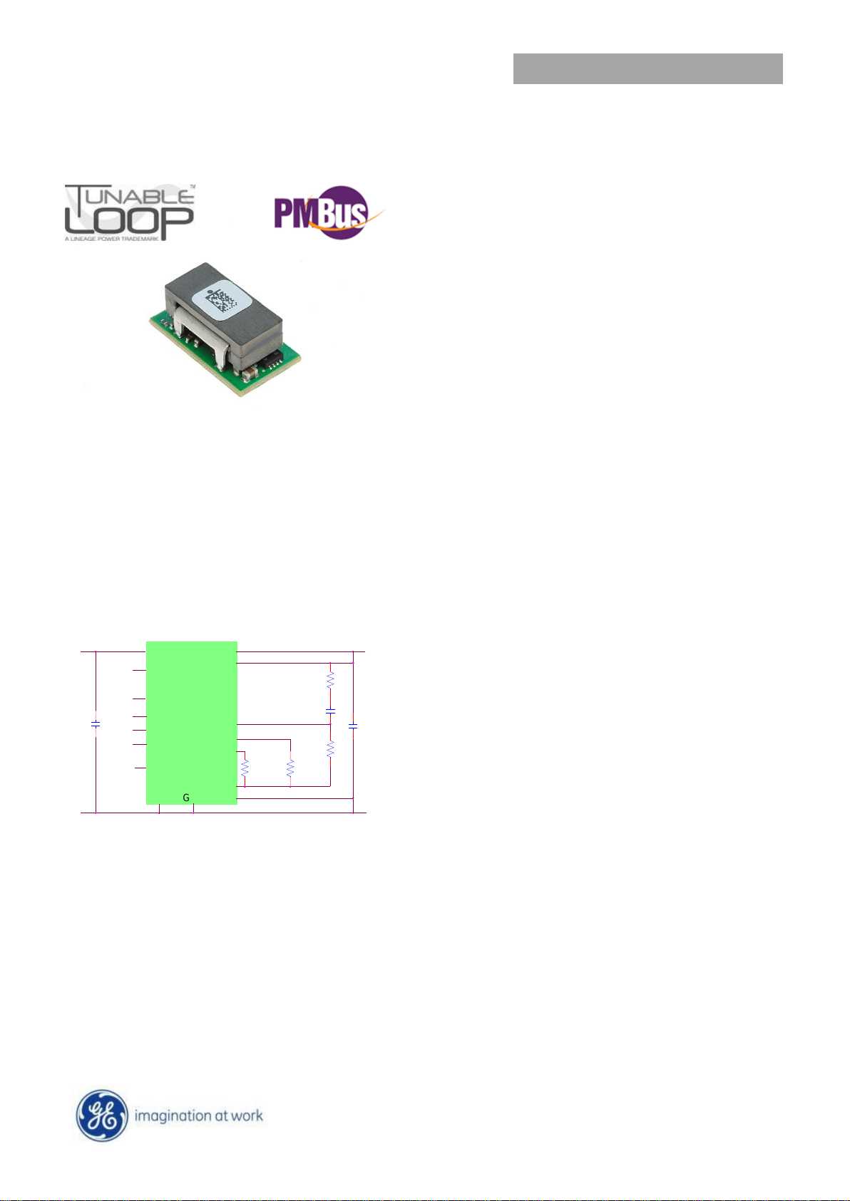
Small size: 20.32 mm x 11.43 mm x 8.5 mm (0.8 in x
0.45 in x 0.334 in)
Wide operating temperature range [-40°C to 85°C]
UL* 60950-1 2
nd
Ed. Recognized, CSA† C22.2 No. 60950-1-07
Certified, and VDE‡ (EN60950-1 2nd Ed.) Licensed
ISO** 9001 and ISO 14001 certified manufacturing facilities
Applications
Distributed power architectures
Intermediate bus voltage applications
Telecommunications equipment
Servers and storage applications
Networking equipment
Industrial equipment
Description
The 20A Digital MicroDLynxTM power modules are non-isolated dc-dc converters that can deliver up to 20A of output current.
These modules operate over a wide range of input voltage (VIN = 3Vdc-14.4Vdc) and provide a precisely regulated output voltage
from 0.6Vdc to 5.5Vdc, programmable via an external resistor and PMBusTM control. Features include a digital interface using the
PMBus
TM
protocol, remote On/Off, adjustable output voltage, over current and over temperature protection. The PMBus
TM #
interface supports a range of commands to both control and monitor the module. The module also includes the Tunable LoopTM
feature that allows the user to optimize the dynamic response of the converter to match the load with reduced amount of output
capacitance leading to savings on cost and PWB area.
* UL is a registered trademark of Underwriters Laboratories, Inc.
†
CSA is a registered trademark of Canadian Standards Association.
‡
VDE is a trademark of Verband Deutscher Elektrotechniker e.V.
** ISO is a registered trademark of the International Organization of Standards
#
The PMBus name and logo are registered trademarks of the System Management Interface Forum (SMIF)
TRIM
VOUT
VS+
GND
RTUNE
CTUNE
RTrim
VIN
Co
Cin
Vout+
Vin+
ON/OFF
SEQ
MODULE
PGOOD
SMBALRT#
SIG_GND
ADDR1
RADDR0
CLK
DATA
ADDR0
VS-
RADDR1
GND
SYNC
RoHS Compliant
20A Digital MicroDLynxTM: Non-Isolated DC-DC Power Modules
3Vdc –14.4Vdc input; 0.45Vdc to 5.5Vdc output; 20A Output Current
Page 2
GE
Data Sheet
20A Digital MicroDLynxTM: Non-Isolated DC-DC Power Modules
3Vdc –14.4Vdc input; 0.45Vdc to 5.5Vdc output; 20A Output Current
April 24, 2013
©2012 General Electric Company. All rights reserved.
Page 2
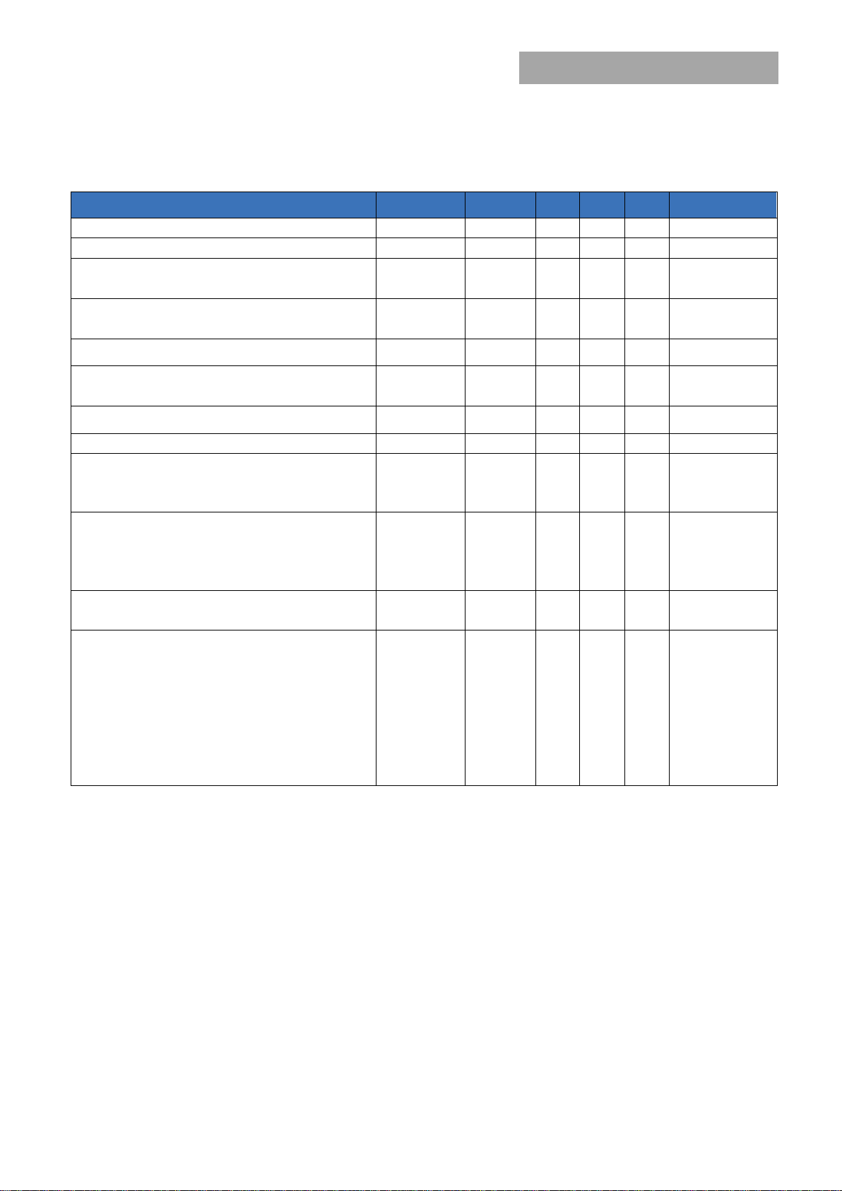
Parameter
Device
Symbol
Min
Max
Unit
Input Voltage
All
V
IN
-0.3
15
V
Continuous
SEQ, SYNC, VS+
All 7 V
CLK, DATA, SMBALERT#
All
3.6
V
Operating Ambient Temperature
All
TA -40
85
°C
(see Thermal Considerations section)
Storage Temperature
All
T
stg
-55
125
°C
Parameter
Device
Symbol
Min
Typ
Max
Unit
Operating Input Voltage
All
VIN
3 14.4
Vdc
Maximum Input Current
All
I
IN,max
19
Adc
(VIN=3V to 14V, IO=I
O, max
)
Input No Load Current
(VIN = 12Vdc, IO = 0, module enabled)
V
O,set
=
0.6 Vdc
I
IN,No load
69 mA
V
O,set
=
5Vdc
I
IN,No load
134 mA
Input Stand-by Current
(VIN = 12Vdc, module disabled)
All
I
IN,stand-by
16.4 mA
Inrush Transient
All
I2t
1
A2s
Input Reflected Ripple Current, peak-to-peak
(5Hz to 20MHz, 1μH source impedance; VIN =0 to 14V, IO= I
Omax
;
See Test Configurations)
All
50 mAp-p
Input Ripple Rejection (120Hz)
All
-64 dB
Absolute Maximum Ratings
Stresses in excess of the absolute maximum ratings can cause permanent damage to the device. These are absolute stress ratings
only, functional operation of the device is not implied at these or any other conditions in excess of those given in the operations
sections of the data sheet. Exposure to absolute maximum ratings for extended periods can adversely affect the device reliability.
Electrical Specifications
Unless otherwise indicated, specifications apply over all operating input voltage, resistive load, and temperature conditions.
Page 3
GE
Data Sheet
20A Digital MicroDLynxTM: Non-Isolated DC-DC Power Modules
3Vdc –14.4Vdc input; 0.45Vdc to 5.5Vdc output; 20A Output Current
April 24, 2013
©2012 General Electric Company. All rights reserved.
Page 3
Parameter
Device
Symbol
Min
Typ
Max
Unit
Output Voltage Set-point (with 0.1% tolerance for external
resistor used to set output voltage)
All
V
O, set
-1.0 +1.0
% V
O, set
Output Voltage (Over all operating input voltage, resistive
load, and temperature conditions until end of life)
All
V
O, set
-3.0 +3.0
% V
O, set
Adjustment Range (selected by an external resistor)
(Some output voltages may not be possible depending on
the input voltage – see Feature Descriptions Section)
All
VO 0.6 5.5
Vdc
PMBus Adjustable Output Voltage Range
All
VO,adj
-25 0 +25
%V
O,set
PMBus Output Voltage Adjustment Step Size
All
0.4
%V
O,set
Remote Sense Range
All
0.5
Vdc
Output Regulation (for VO ≥ 2.5Vdc)
Line (VIN=V
IN, min
to V
IN, max
)
All
+0.4
% V
O, set
Load (IO=I
O, min
to I
O, max
)
All
10
mV
Output Regulation (for VO < 2.5Vdc)
Line (VIN=V
IN, min
to V
IN, max
)
All
5
mV
Load (IO=I
O, min
to I
O, max
)
All
10
mV
Temperature (T
ref=TA, min
to T
A, max
)
All
0.4
% V
O, set
Output Ripple and Noise on nominal output
(VIN=V
IN, nom
and IO=I
O, min
to I
O, max
Co = 0.1μF // 22 μF
ceramic capacitors)
Peak-to-Peak (5Hz to 20MHz bandwidth)
All
50
100
mV
pk-pk
RMS (5Hz to 20MHz bandwidth)
All
20
38
mV
rms
External Capacitance1
Without the Tunable Loop
TM
ESR ≥ 1 mΩ
All
C
O, max
2x47 2x47
μF
With the Tunable Loop
TM
ESR ≥ 0.15 mΩ
All
C
O, max
2x47 1000
μF
ESR ≥ 10 mΩ
All
C
O, max
2x47
10000
μF
Output Current (in either sink or source mode)
All
Io 0 20
Adc
Output Current Limit Inception (Hiccup Mode)
(current limit does not operate in sink mode)
All
I
O, lim
130 % I
o,max
Output Short-Circuit Current
All
I
O, s/c
1.4 Arms
(VO≤250mV) ( Hiccup Mode )
Efficiency
V
O,set
= 0.6Vdc
η 79.2 %
VIN= 12Vdc, TA=25°C
V
O, set
= 1.2Vdc
η 87.1 %
IO=I
O, max , VO
= V
O,set
V
O,set
= 1.8Vdc
η 90.4 %
V
O,set
= 2.5Vdc
η 92.6 %
V
O,set
= 3.3Vdc
η 93.8 %
V
O,set
= 5.0Vdc
η 95.2 %
Switching Frequency
All
f
sw
500 kHz
Electrical Specifications (continued)
1
External capacitors may require using the new Tunable LoopTM feature to ensure that the module is stable as well as getting the best
transient response. See the Tunable LoopTM section for details.
Page 4
GE
Data Sheet
20A Digital MicroDLynxTM: Non-Isolated DC-DC Power Modules
3Vdc –14.4Vdc input; 0.45Vdc to 5.5Vdc output; 20A Output Current
April 24, 2013
©2012 General Electric Company. All rights reserved.
Page 4
Parameter
Device
Symbol
Min
Typ
Max
Unit
Frequency Synchronization
All
Synchronization Frequency Range
All
425 600
kHz
High-Level Input Voltage
All
V
IH
2.0 V Low-Level Input Voltage
All
V
IL
0.4
V
Input Current, SYNC
All
I
SYNC
100
nA
Minimum Pulse Width, SYNC
All
t
SYNC
100
ns
Maximum SYNC rise time
All
t
SYNC_SH
100
ns
Parameter
Device
Min
Typ
Max
Unit
Calculated MTBF (IO=0.8I
O, max
, TA=40°C) Telecordia Issue 2
Method 1 Case 3
All
15,455,614
Hours
Weight
4.54 (0.16)
g (oz.)
Parameter
Device
Symbol
Min
Typ
Max
Unit
On/Off Signal Interface
(VIN=V
IN, min
to V
IN, max
; open collector or equivalent,
Signal referenced to GND)
Device code with suffix “4” – Positive Logic (See Ordering
Information)
Logic High (Module ON)
Input High Current
All
IIH 1
mA
Input High Voltage
All
VIH 2 V
IN,max
V
Logic Low (Module OFF)
Input Low Current
All
IIL
1
mA
Input Low Voltage
All
VIL -0.2 0.6
V
Device Code with no suffix – Negative Logic (See Ordering
Information)
(On/OFF pin is open collector/drain logic input with
external pull-up resistor; signal referenced to GND)
Logic High (Module OFF)
Input High Current
All
IIH ― ― 1 mA
Input High Voltage
All
VIH 2 ―
V
IN, max
Vdc
Logic Low (Module ON)
Input low Current
All
IIL ― ―
10
μA
Input Low Voltage
All
VIL
-0.2 ― 0.6
Vdc
Electrical Specifications (continued)
General Specifications
Feature Specifications
Unless otherwise indicated, specifications apply overall operating input voltage, resistive load, and temperature conditions. See
Feature Descriptions for additional information.
Page 5
GE
Data Sheet
20A Digital MicroDLynxTM: Non-Isolated DC-DC Power Modules
3Vdc –14.4Vdc input; 0.45Vdc to 5.5Vdc output; 20A Output Current
April 24, 2013
©2012 General Electric Company. All rights reserved.
Page 5
Parameter
Device
Symbol
Min
Typ
Max
Units
Turn-On Delay and Rise Times
(VIN=V
IN, nom
, IO=I
O, max , VO
to within ±1% of steady state)
Case 1: On/Off input is enabled and then input power is
applied (delay from instant at which VIN = V
IN, min
until Vo =
10% of Vo, set)
All
Tdelay
―
1.2 ― msec
Case 2: Input power is applied for at least one second and
then the On/Off input is enabled (delay from instant at
which Von/Off is enabled until Vo = 10% of Vo, set)
All
Tdelay
―
0.8 ― msec
Output voltage Rise time (time for Vo to rise from
10% of Vo, set to 90% of Vo, set)
All
Trise
―
2.7 ― msec
Output voltage overshoot (TA = 25oC
VIN= V
IN, min
to V
IN, max,IO
= I
O, min
to I
O, max
)
With or without maximum external capacitance
3.0
% V
O, set
Over Temperature Protection
(See Thermal Considerations section)
All
T
ref
120
°C
PMBus Over Temperature Warning Threshold *
All
T
WARN
120 °C
Tracking Accuracy (Power-Up: 2V/ms)
All
VSEQ –Vo
100
mV
(Power-Down: 2V/ms)
All
VSEQ –Vo
100
mV
(V
IN, min
to V
IN, max
; I
O, min
to I
O, max
VSEQ < Vo)
Input Undervoltage Lockout
Turn-on Threshold
All
3.25
Vdc
Turn-off Threshold
All
2.6
Vdc
Hysteresis
All
0.25 Vdc
PMBus Adjustable Input Under Voltage Lockout Thresholds
All
2.5 14
Vdc
Resolution of Adjustable Input Under Voltage Threshold
All
500
mV
PGOOD (Power Good)
Signal Interface Open Drain, V
supply
5VDC
Overvoltage threshold for PGOOD ON
All
108 %V
O, set
Overvoltage threshold for PGOOD OFF
All
105 %V
O, set
Undervoltage threshold for PGOOD ON
All
110 %V
O, set
Undervoltage threshold for PGOOD OFF
All
90 %V
O, set
Pulldown resistance of PGOOD pin
All
50
Sink current capability into PGOOD pin
All
5
mA
Feature Specifications (cont.)
* Over temperature Warning – Warning may not activate before alarm and unit may shutdown before warning
Page 6
GE
Data Sheet
20A Digital MicroDLynxTM: Non-Isolated DC-DC Power Modules
3Vdc –14.4Vdc input; 0.45Vdc to 5.5Vdc output; 20A Output Current
April 24, 2013
©2012 General Electric Company. All rights reserved.
Page 6
Parameter
Conditions
Symbol
Min
Typ
Max
Unit
PMBus Signal Interface Characteristics
Input High Voltage (CLK, DATA)
VIH
2.1 3.6 V Input Low Voltage (CLK, DATA)
VIL
0.8
V
Input high level current (CLK, DATA)
IIH
-10 10
μA
Input low level current (CLK, DATA)
IIL
-10 10
μA
Output Low Voltage (CLK, DATA, SMBALERT#)
I
OUT
=2mA
VOL
0.4
V
Output high level open drain leakage current (DATA,
SMBALERT#)
V
OUT
=3.6V
I
OH
0 10
μA
Pin capacitance
CO
0.7 pF
PMBus Operating frequency range
Slave Mode
FPMB
10 400
kHz
Data hold time
Receive Mode
Transmit Mode
tHD:DAT
0
300
ns
Data setup time
tSU:DAT
250
ns
Measurement System Characteristics
Read delay time
tDLY
153
192
231
μs
Output current measurement range
I
RNG
0 26
A
Output current measurement resolution
IRES
62.5
mA
Output current measurement accuracy at 25°C (with I
OUT,
CORR
)
I
ACC
±5
%
Output current measurement offset
I
OFST
0.1 A V
OUT
measurement range
V
OUT(rng)
0 5.5
V
V
OUT
measurement resolution
V
OUT(res)
15.62
5
mV
V
OUT
measurement accuracy
V
OUT, ACC
-15 5
%
V
OUT
measurement offset
V
OUT(ofst)
-3 3 % VIN measurement range
V
IN(rng)
0 14.4
V
VIN measurement resolution
V
IN(res)
32.5 mV
VIN measurement accuracy
V
IN, ACC
-15 5
%
VIN measurement offset
V
IN(ofst)
-5.5
-2
1.4
LSB
Digital Interface Specifications
Unless otherwise indicated, specifications apply over all operating input voltage, resistive load, and temperature conditions. See
Feature Descriptions for additional information.
Page 7
GE
Data Sheet
20A Digital MicroDLynxTM: Non-Isolated DC-DC Power Modules
3Vdc –14.4Vdc input; 0.45Vdc to 5.5Vdc output; 20A Output Current
April 24, 2013
©2012 General Electric Company. All rights reserved.
Page 7
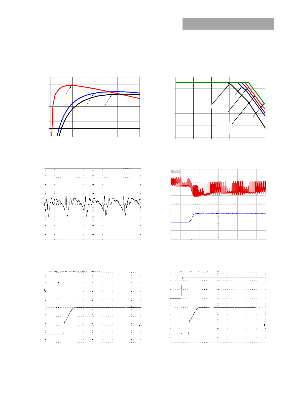
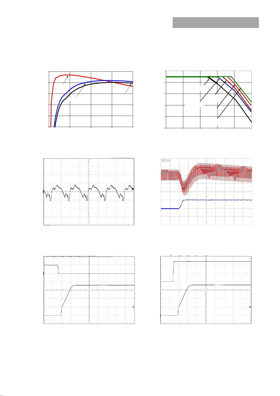
EFFICIENCY, (%)
OUTPUT CURRENT, Io (A)
OUTPUT CURRENT, IO (A)
AMBIENT TEMPERATURE, TA OC
Figure 1. Converter Efficiency versus Output Current.
Figure 2. Derating Output Current versus Ambient Temperature
and Airflow.
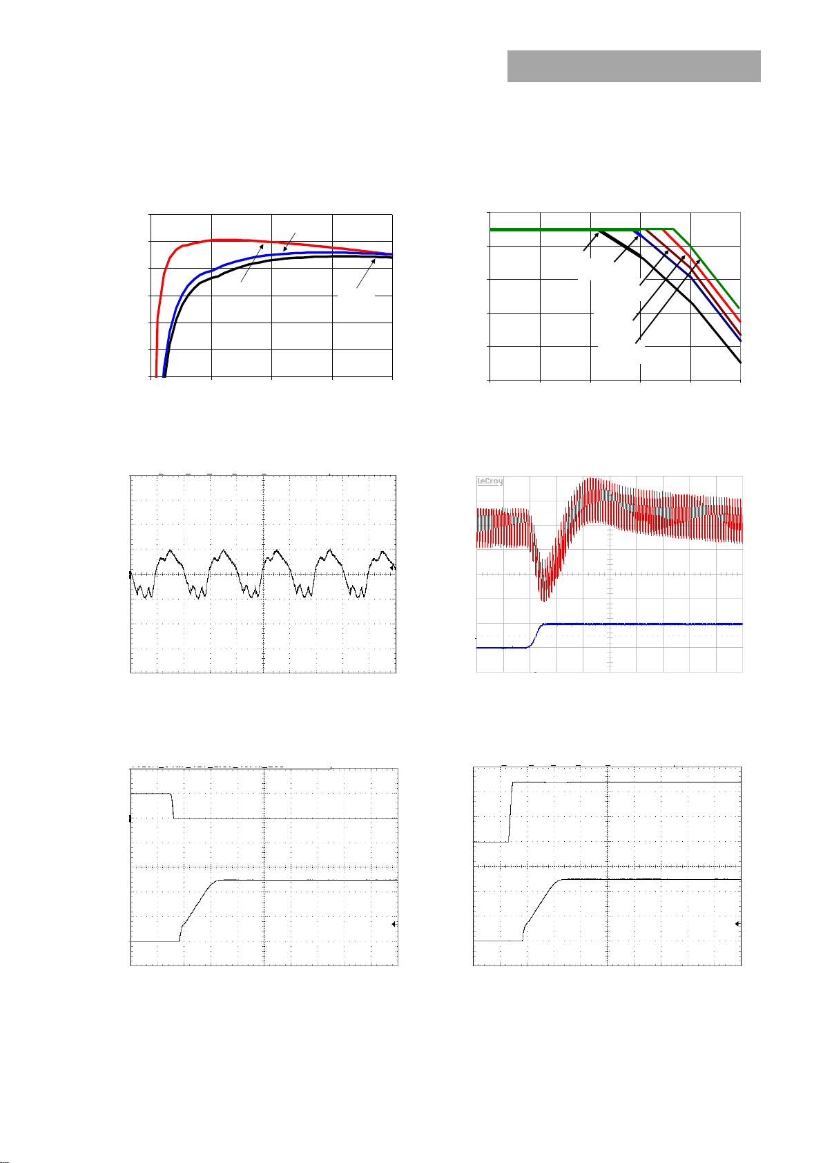
OUTPUT VOLTAGE
V
O
(V) (10mV/div)
OUTPUT CURRENT, OUTPUT OLTAGE
I
O
(A) (10Adiv) V
O
(V) (10mV/div)
TIME, t (1s/div)
TIME, t (20s /div)
Figure 3. Typical output ripple and noise (CO=2x47μF
ceramic, VIN = 12V, Io = Io,max, ).
Figure 4. Transient Response to Dynamic Load Change from 50%
to 100% at 12Vin, Cout= 1x47uF +11x330uF CTune=47nF,
RTune=178 ohms
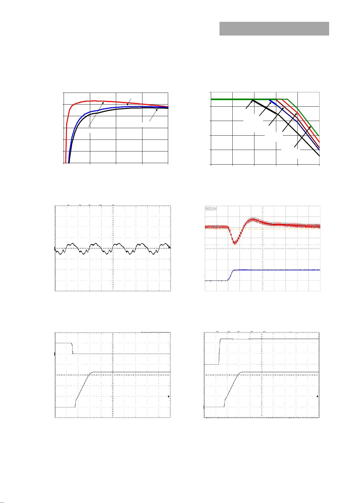
OUTPUT VOLTAGE ON/OFF VOLTAGE
V
O
(V) (200mV/div) V
ON/OFF
(V) (5V/div)
OUTPUT VOLTAGE INPUT VOLTAGE
V
O
(V) (200mV/div) V
IN
(V) (5V/div)
TIME, t (2ms/div)
TIME, t (2ms/div)
Figure 5. Typical Start-up Using On/Off Voltage (Io = Io,max).
Figure 6. Typical Start-up Using Input Voltage (VIN = 12V, Io = Io,max).
50
55
60
65
70
75
80
85
90
0 5 10 15 20
Vin=3.3V
Vin=14V
Vin=12V
2
6
10
14
18
22
55 65 75 85 95 105
0.5m/s
(100LFM)
1.5m/s
(300LFM)
1m/s
(200LFM)
NC
2m/s
(400LFM)
Characteristic Curves
The following figures provide typical characteristics for the 20A Digital MicroDLynxTM at 0.6Vo and 25oC.
Page 8
GE
Data Sheet
20A Digital MicroDLynxTM: Non-Isolated DC-DC Power Modules
3Vdc –14.4Vdc input; 0.45Vdc to 5.5Vdc output; 20A Output Current
April 24, 2013
©2012 General Electric Company. All rights reserved.
Page 8
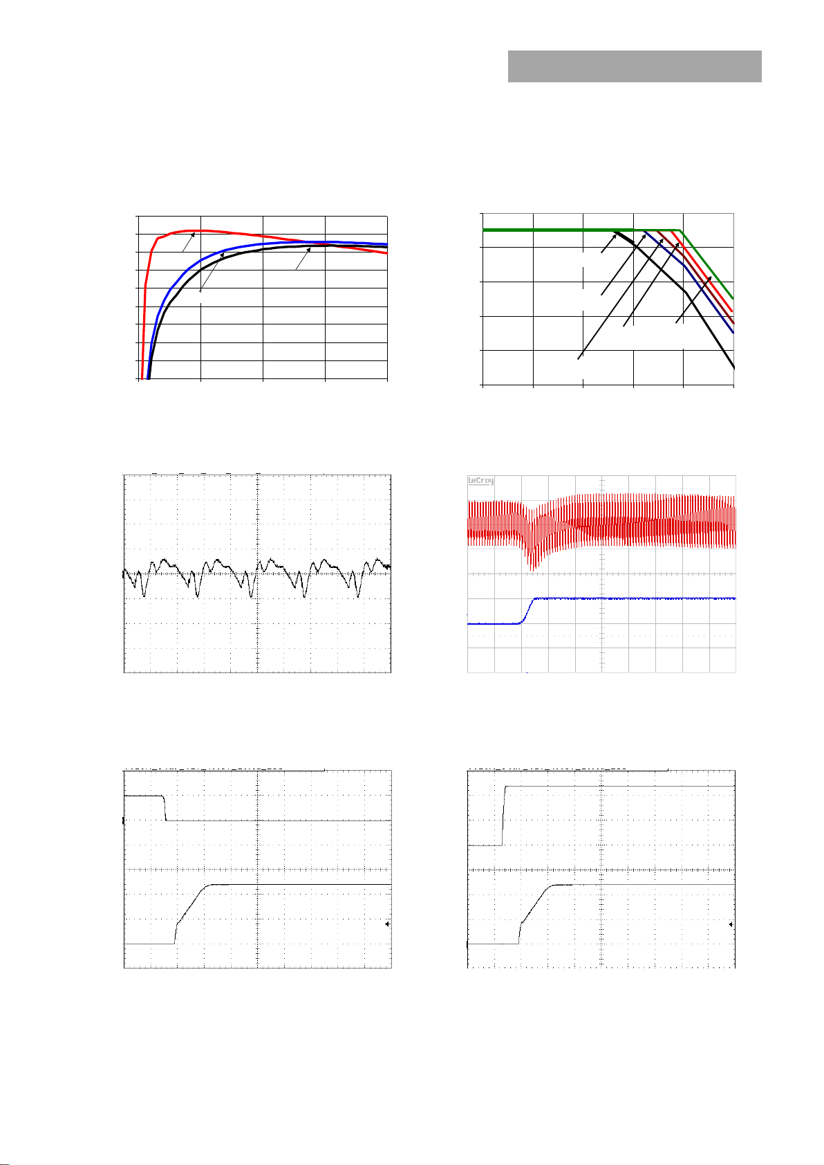
EFFICIENCY, (%)
OUTPUT CURRENT, Io (A)
OUTPUT CURRENT, IO (A)
AMBIENT TEMPERATURE, TA OC
Figure 7. Converter Efficiency versus Output Current.
Figure 8. Derating Output Current versus Ambient Temperature
and Airflow.
OUTPUT VOLTAGE
V
O
(V) (20mV/div)
OUTPUT CURRENT, OUTPUT VOLTAGE
I
O
(A) (10Adiv) V
O
(V) (20mV/div)
TIME, t (1s/div)
TIME, t (20s /div)
Figure 9. Typical output ripple and noise (CO=2x47μF
ceramic, VIN = 12V, Io = Io,max, ).
Figure 10. Transient Response to Dynamic Load Change from
50% to 100% at 12Vin, Cout= 1x47uF +5x330uF, CTune=10nF &
RTune=178 ohms
OUTPUT VOLTAGE ON/OFF VOLTAGE
V
O
(V) (500mV/div) V
ON/OFF
(V) (5V/div)
OUTPUT VOLTAGE INPUT VOLTAGE
V
O
(V) (500mV/div) V
IN
(V) (5V/div)
TIME, t (2ms/div)
TIME, t (2ms/div)
Figure 11. Typical Start-up Using On/Off Voltage (Io = Io,max).
Figure 12. Typical Start-up Using Input Voltage (VIN = 12V, Io =
Io,max).
50
55
60
65
70
75
80
85
90
95
0 5 10 15 20
Vin=3.3V
Vin=14V
Vin=12V
2
6
10
14
18
22
55 65 75 85 95 105
2m/s
(400LFM)
1.5m/s
(300LFM)
1m/s
(200LFM)
0.5m/s
(100LFM)
NC
Characteristic Curves
The following figures provide typical characteristics for the 20A Digital MicroDLynxTM at 1.2Vo and 25oC.
Page 9
GE
Data Sheet
20A Digital MicroDLynxTM: Non-Isolated DC-DC Power Modules
3Vdc –14.4Vdc input; 0.45Vdc to 5.5Vdc output; 20A Output Current
April 24, 2013
©2012 General Electric Company. All rights reserved.
Page 9
EFFICIENCY, (%)
OUTPUT CURRENT, Io (A)
OUTPUT CURRENT, IO (A)
AMBIENT TEMPERATURE, TA OC
Figure 13. Converter Efficiency versus Output Current.
Figure 14. Derating Output Current versus Ambient
Temperature and Airflow.
OUTPUT VOLTAGE
V
O
(V) (20mV/div)
OUTPUT CURRENT, OUTPUT VOLTAGE
I
O
(A) (10Adiv) V
O
(V) (20mV/div)
TIME, t (1s/div)
TIME, t (20s /div)
Figure 15. Typical output ripple and noise (CO=2X47μF
ceramic, VIN = 12V, Io = Io,max, ).
Figure 16. Transient Response to Dynamic Load Change from
50% to 100% at 12Vin, Cout= 2x47uF +3x330uF, CTune=5600pF
& RTune=220 ohms
OUTPUT VOLTAGE ON/OFF VOLTAGE
V
O
(V) (500mV/div) V
ON/OFF
(V) 5V/div)
OUTPUT VOLTAGE INPUT VOLTAGE
V
O
(V) (500mV/div) V
IN
(V) (5V/div)
TIME, t (2ms/div)
TIME, t (2ms/div)
Figure 17. Typical Start-up Using On/Off Voltage (Io = Io,max).
Figure 18. Typical Start-up Using Input Voltage (VIN = 12V, Io =
Io,max).
70
75
80
85
90
95
0 5 10 15 20
Vin=3.3V
Vin=14V
Vin=12V
2
6
10
14
18
22
55 65 75 85 95 105
2m/s
(400LFM)
1.5m/s
(300LFM)
1m/s
(200LFM)
0.5m/s
(100LFM)
NC
Characteristic Curves
The following figures provide typical characteristics for the 20A Digital MicroDLynxTM at 1.8Vo and 25oC.
Page 10
GE
Data Sheet
20A Digital MicroDLynxTM: Non-Isolated DC-DC Power Modules
3Vdc –14.4Vdc input; 0.45Vdc to 5.5Vdc output; 20A Output Current
April 24, 2013
©2012 General Electric Company. All rights reserved.
Page 10
EFFICIENCY, (%)
OUTPUT CURRENT, Io (A)
OUTPUT CURRENT, IO (A)
AMBIENT TEMPERATURE, TA OC
Figure 19. Converter Efficiency versus Output Current.
Figure 20. Derating Output Current versus Ambient
Temperature and Airflow.
OUTPUT VOLTAGE
V
O
(V) (20mV/div)
OUTPUT CURRENT, OUTPUT VOLTAGE
I
O
(A) (10Adiv) V
O
(V) (20mV/div)
TIME, t (1s/div)
TIME, t (20s /div)
Figure 21. Typical output ripple and noise (CO=2x47μF ceramic,
VIN = 12V, Io = Io,max, ).
Figure 22. Transient Response to Dynamic Load Change from
50% to 100% at 12Vin, Cout= 2x47uF +2x330uF, CTune=3300pF
& RTune=220 ohms
OUTPUT VOLTAGE ON/OFF VOLTAGE
V
O
(V) (1V/div) V
ON/OFF
(V) (5V/div)
OUTPUT VOLTAGE INPUT VOLTAGE
V
O
(V) (1V/div) V
IN
(V) (5V/div)
TIME, t (2ms/div)
TIME, t (2ms/div)
Figure 23. Typical Start-up Using On/Off Voltage (Io = Io,max).
Figure 24. Typical Start-up Using Input Voltage (VIN = 12V, Io =
Io,max).
70
75
80
85
90
95
100
0 5 10 15 20
Vin=4.5V
Vin=14V
Vin=12V
2
6
10
14
18
22
55 65 75 85 95 105
2m/s
(400LFM)
1.5m/s
(300LFM)
1m/s
(200LFM)
0.5m/s
(100LFM)
NC
Characteristic Curves
The following figures provide typical characteristics for the 20A Digital MicroDLynxTM at 2.5Vo and 25oC.
Page 11
GE
Data Sheet
20A Digital MicroDLynxTM: Non-Isolated DC-DC Power Modules
3Vdc –14.4Vdc input; 0.45Vdc to 5.5Vdc output; 20A Output Current
April 24, 2013
©2012 General Electric Company. All rights reserved.
Page 11
EFFICIENCY, (%)
OUTPUT CURRENT, Io (A)
OUTPUT CURRENT, IO (A)
AMBIENT TEMPERATURE, TA OC
Figure 25. Converter Efficiency versus Output Current.
Figure 26. Derating Output Current versus Ambient Temperature
and Airflow.
OUTPUT VOLTAGE
V
O
(V) (50mV/div)
OUTPUT CURRENT, OUTPUT VOLTAGE
I
O
(A) (10Adiv) V
O
(V) (50mV/div)
TIME, t (1s/div)
TIME, t (20s /div)
Figure 27. Typical output ripple and noise (CO=2x47μF
ceramic, VIN = 12V, Io = Io,max, ).
Figure 28 Transient Response to Dynamic Load Change from
50% to 100% at 12Vin, Cout= 5x47uF +1x330uF, CTune=2200pF &
RTune=220 ohms
OUTPUT VOLTAGE ON/OFF VOLTAGE
V
O
(V) (1V/div) V
ON/OFF
(V) (5V/div)
OUTPUT VOLTAGE INPUT VOLTAGE
V
O
(V) (1V/div) V
IN
(V) (5V/div)
TIME, t (2ms/div)
TIME, t (2ms/div)
Figure 29. Typical Start-up Using On/Off Voltage (Io = Io,max).
Figure 30. Typical Start-up Using Input Voltage (VIN = 12V, Io =
Io,max).
70
75
80
85
90
95
100
0 5 10 15 20
Vin=4.5V
Vin=14V
Vin=12V
2
6
10
14
18
22
55 65 75 85 95 105
2m/s
(400LFM)
1.5m/s
(300LFM)
1m/s
(200LFM)
0.5m/s
(100LFM)
NC
2m/s
(400LFM)
1.5m/s
(300LFM)
1m/s
(200LFM)
0.5m/s
(100LFM)
NC
Characteristic Curves
The following figures provide typical characteristics for the 20A Digital MicroDLynxTM at 3.3Vo and 25oC.
Page 12
GE
Data Sheet
20A Digital MicroDLynxTM: Non-Isolated DC-DC Power Modules
3Vdc –14.4Vdc input; 0.45Vdc to 5.5Vdc output; 20A Output Current
April 24, 2013
©2012 General Electric Company. All rights reserved.
Page 12
EFFICIENCY, (%)
OUTPUT CURRENT, Io (A)
OUTPUT CURRENT, IO (A)
AMBIENT TEMPERATURE, TA OC
Figure 31. Converter Efficiency versus Output Current.
Figure 32. Derating Output Current versus Ambient Temperature
and Airflow.
OUTPUT VOLTAGE
V
O
(V) (50mV/div)
OUTPUT CURRENT, OUTPUT VOLTAGE
I
O
(A) (10Adiv) V
O
(V) (50mV/div)
TIME, t (1s/div)
TIME, t (20s /div)
Figure 33. Typical output ripple and noise (CO=2x47μF
ceramic, VIN = 12V, Io = Io,max, ).
Figure 34. Transient Response to Dynamic Load Change from
50% to 100% at 12Vin, Cout= 8x47uF, CTune=1500pF &
RTune=220 ohms
OUTPUT VOLTAGE ON/OFF VOLTAGE
V
O
(V) (2V/div) V
ON/OFF
(V) (5V/div)
OUTPUT VOLTAGE INPUT VOLTAGE
V
O
(V) (2V/div) V
IN
(V) (5V/div)
TIME, t (2ms/div)
TIME, t (2ms/div)
Figure 35. Typical Start-up Using On/Off Voltage (Io = Io,max).
Figure 36. Typical Start-up Using Input Voltage (VIN = 12V, Io =
Io,max).
70
75
80
85
90
95
100
0 5 10 15 20
Vin=7V
Vin=12V
Vin=14V
2
6
10
14
18
22
55 65 75 85 95 105
2m/s
(400LFM)
1.5m/s
(300LFM)
1m/s
(200LFM)
0.5m/s
(100LFM)
NC
Characteristic Curves
The following figures provide typical characteristics for the 20A Digital MicroDLynxTM at 5Vo and 25oC.
Page 13

GE
Data Sheet
20A Digital MicroDLynxTM: Non-Isolated DC-DC Power Modules
3Vdc –14.4Vdc input; 0.45Vdc to 5.5Vdc output; 20A Output Current
April 24, 2013
©2012 General Electric Company. All rights reserved.
Page 13
Input Ripple Voltage (mVp-p)
Output Voltage (Vdc)
0
50
100
150
200
250
300
350
400
450
0.5 1 1.5 2 2.5 3 3.5 4 4.5 5
2x22uF
3x22 uF
0
10
20
30
40
50
60
70
0.5 1 1.5 2 2.5 3 3.5 4 4.5 5
Ripple (mVp-p)
Output Voltage(Volts)
2x47uF Ext Cap
4x47uF Ext Cap
6x47uF Ext Cap
8x47uF Ext Cap
Design Considerations
Input Filtering
The 20A Digital MicroDLynxTM module should be
connected to a low ac-impedance source. A highly
inductive source can affect the stability of the module. An
input capacitance must be placed directly adjacent to the
input pin of the module, to minimize input ripple voltage
and ensure module stability.
To minimize input voltage ripple, ceramic capacitors are
recommended at the input of the module. Figure 37
shows the input ripple voltage for various output voltages
at 20A of load current with 2x22 µF or 3x22 µF ceramic
capacitors and an input of 12V.
Figure 38. Output ripple voltage for various output
voltages with external 2x47 µF, 4x47 µF or 6x47 µF
ceramic capacitors at the output (20A load). Input voltage
is 12V.
Safety Considerations
For safety agency approval the power module must be
installed in compliance with the spacing and separation
requirements of the end-use safety agency standards, i.e.,
UL 60950-1 2nd, CSA C22.2 No. 60950-1-07, DIN EN 609501:2006 + A11 (VDE0805 Teil 1 + A11):2009-11; EN 609501:2006 + A11:2009-03.
Figure 37. Input ripple voltage for various output
voltages with 2x22 µF or 3x22 µF ceramic capacitors at
the input (20A load). Input voltage is 12V.
Output Filtering
These modules are designed for low output ripple voltage
and will meet the maximum output ripple specification with
0.1 µF ceramic and 2x47 µF ceramic capacitors at the
output of the module. However, additional output filtering
may be required by the system designer for a number of
reasons. First, there may be a need to further reduce the
output ripple and noise of the module. Second, the dynamic
response characteristics may need to be customized to a
particular load step change.
To reduce the output ripple and improve the dynamic
response to a step load change, additional capacitance at
the output can be used. Low ESR polymer and ceramic
capacitors are recommended to improve the dynamic
response of the module. Figure 38 provides output ripple
information for different external capacitance values at
various Vo and a full load current of 20A. For stable
operation of the module, limit the capacitance to less than
the maximum output capacitance as specified in the
electrical specification table. Optimal performance of the
module can be achieved by using the Tunable LoopTM
feature described later in this data sheet.
For the converter output to be considered meeting the
requirements of safety extra-low voltage (SELV), the input
must meet SELV requirements. The power module has
extra-low voltage (ELV) outputs when all inputs are ELV.
The UDT020A0X series were tested using an external
Littelfuse 456 series fast-acting fuse rated at 30 A, 100 Vdc
in the ungrounded input.
Page 14

GE
Data Sheet
20A Digital MicroDLynxTM: Non-Isolated DC-DC Power Modules
3Vdc –14.4Vdc input; 0.45Vdc to 5.5Vdc output; 20A Output Current
April 24, 2013
©2012 General Electric Company. All rights reserved.
Page 14
20K
Rpullup
I
20K
ON/OFF
+
20K
3.3V
470
VIN
20K
Q7
20K
100pF
4.7K
ENABLE
100K
DLYNX MODULE
47K
Q2
+VIN
20K
GND
20K
20K
2K
ON/OFF
Q6
Q5
V
Q3
_
ENABLE
470
4.7K
+VIN
20K
100K
2K
100pF
_
47K
GND
Q6
20K
Q2
+
DLYNX MODULE
V
Rpullup
Q3
ON/OFF
20K
I
ON/OFF
3.3V
Q5
20K
Analog Feature Descriptions
Remote On/Off
Digital On/Off
Please see the Digital Feature Descriptions section.
The module can be turned ON and OFF either by using the
ON/OFF pin (Analog interface) or through the PMBus
interface (Digital). The module can be configured in a
number of ways through the PMBus interface to react to the
two ON/OFF inputs:
Module ON/OFF can be controlled only through
the analog interface (digital interface ON/OFF
commands are ignored)
Module ON/OFF can be controlled only through
the PMBus interface (analog interface is ignored)
Module ON/OFF can be controlled by either the
analog or digital interface
Figure 39. Circuit configuration for using positive On/Off
logic.
The default state of the module (as shipped from the factory)
is to be controlled by the analog interface only. If the digital
interface is to be enabled, or the module is to be controlled
only through the digital interface, this change must be made
through the PMBus. These changes can be made and
written to non-volatile memory on the module so that it is
remembered for subsequent use.
Analog On/Off
The 20A Digital MicroDLynxTM power modules feature an
On/Off pin for remote On/Off operation. Two On/Off logic
options are available. In the Positive Logic On/Off option,
(device code suffix “4” – see Ordering Information), the
module turns ON during a logic High on the On/Off pin and
turns OFF during a logic Low. With the Negative Logic
On/Off option, (no device code suffix, see Ordering
Information), the module turns OFF during logic High and ON
during logic Low. The On/Off signal should be always
referenced to ground. For either On/Off logic option, leaving
the On/Off pin disconnected will turn the module ON when
input voltage is present.
For positive logic modules, the circuit configuration for using
the On/Off pin is shown in Figure 39. When the external
transistor Q2 is in the OFF state, the internal transistor Q7 is
turned ON, which turn Q3 OFF which keeps Q6 OFF and Q5
OFF. This allows the internal PWM #Enable signal to be
pulled up by the internal 3.3V, thus turning the module ON.
When transistor Q2 is turned ON, the On/Off pin is pulled
low, which turns Q7 OFF which turns Q3, Q6 and Q5 ON and
the internal PWM #Enable signal is pulled low and the
module is OFF. A suggested value for R
pullup
is 20k.
For negative logic On/Off modules, the circuit configuration
is shown in Fig. 40. The On/Off pin should be pulled high with
an external pull-up resistor (suggested value for the 3V to
14V input range is 20Kohms). When transistor Q2 is in the
OFF state, the On/Off pin is pulled high, transistor Q3 is
turned ON. This turns Q6 ON, followed by Q5 turning ON
which pulls the internal ENABLE low and the module is OFF.
To turn the module ON, Q2 is turned ON pulling the On/Off
pin low, turning transistor Q3 OFF, which keeps Q6 and Q5
OFF resulting in the PWM Enable pin going high.
Figure 40. Circuit configuration for using negative On/Off
logic.
Monotonic Start-up and Shutdown
The module has monotonic start-up and shutdown behavior
for any combination of rated input voltage, output current
and operating temperature range.
Startup into Pre-biased Output
The module can start into a prebiased output as long as the
prebias voltage is 0.5V less than the set output voltage.
Analog Output Voltage Programming
The output voltage of the module is programmable to any
voltage from 0.6dc to 5.5Vdc by connecting a resistor
between the Trim and SIG_GND pins of the module. Certain
restrictions apply on the output voltage set point depending
on the input voltage. These are shown in the Output Voltage
vs. Input Voltage Set Point Area plot in Fig. 41. The Upper
Limit curve shows that for output voltages lower than 1V,
the input voltage must be lower than the maximum of
14.4V. The Lower Limit curve shows that for output voltages
higher than 0.6V, the input voltage needs to be larger than
Page 15

GE
Data Sheet
20A Digital MicroDLynxTM: Non-Isolated DC-DC Power Modules
3Vdc –14.4Vdc input; 0.45Vdc to 5.5Vdc output; 20A Output Current
April 24, 2013
©2012 General Electric Company. All rights reserved.
Page 15
V
O
(+)
TRIM
VS─
R
trim
LOAD
V
IN
(+)
ON/OFF
VS+
SIG_GND
k
Vo
Rtrim
6.0
12
V
O, set
(V)
Rtrim (KΩ)
0.6
Open
0.9
40
1.0
30
1.2
20
1.5
13.33
1.8
10
2.5
6.316
3.3
4.444
5.0
2.727
0
2
4
6
8
10
12
14
16
0.5 1 1.5 2 2.5 3 3.5 4 4.5 5 5.5 6
Input Voltage (v)
Output Voltage (V)
Lower
Upper
Vo
MODULE
SIG_GND
Trim
Q1
Rtrim
Rmargin-up
Q2
Rmargin-down
the minimum of 3V. .
Figure 41. Output Voltage vs. Input Voltage Set Point Area
plot showing limits where the output voltage can be set
for different input voltages.
Table 1
Digital Output Voltage Adjustment
Please see the Digital Feature Descriptions section.
Remote Sense
The power module has a Remote Sense feature to minimize
the effects of distribution losses by regulating the voltage
between the sense pins (VS+ and VS-). The voltage drop
between the sense pins and the VOUT and GND pins of the
module should not exceed 0.5V.
Analog Voltage Margining
Output voltage margining can be implemented in the
module by connecting a resistor, R
to the ground pin for margining-up the output voltage and
by connecting a resistor, R
output pin for margining-down. Figure 43 shows the circuit
configuration for output voltage margining. The POL
Caution – Do not connect SIG_GND to GND elsewhere in the
layout
Figure 42. Circuit configuration for programming output
Programming Tool, available at www.lineagepower.com
under the Downloads section, also calculates the values of
R
margin-up
and R
margin-down
for a specific output voltage and %
margin. Please consult your local Lineage Power technical
representative for additional details.
voltage using an external resistor.
Without an external resistor between Trim and SIG_GND
pins, the output of the module will be 0.6Vdc. To calculate
the value of the trim resistor, Rtrim for a desired output
voltage, should be as per the following equation:
Rtrim is the external resistor in kΩ
Vo is the desired output voltage.
Table 1 provides Rtrim values required for some common
output voltages.
Figure 43. Circuit Configuration for margining Output
voltage.
margin-down
, from the Trim pin
margin-up
, from the Trim pin to
Page 16

GE
Data Sheet
20A Digital MicroDLynxTM: Non-Isolated DC-DC Power Modules
3Vdc –14.4Vdc input; 0.45Vdc to 5.5Vdc output; 20A Output Current
April 24, 2013
©2012 General Electric Company. All rights reserved.
Page 16
100 pF
DLynx Module
R1=Rtrim
20K
SIG_GND
SEQ
SEQ
V
Digital Output Voltage Margining
Please see the Digital Feature Descriptions section.
Output Voltage Sequencing
The power module includes a sequencing feature, EZSEQUENCE that enables users to implement various types of
output voltage sequencing in their applications. This is
accomplished via an additional sequencing pin. When not
using the sequencing feature, leave it unconnected.
The voltage applied to the SEQ pin should be scaled down
by the same ratio as used to scale the output voltage down
to the reference voltage of the module. This is accomplished
by an external resistive divider connected across the
sequencing voltage before it is fed to the SEQ pin as shown
in Fig. 44. In addition, a small capacitor (suggested value
100pF) should be connected across the lower resistor R1.
For all DLynx modules, the minimum recommended delay
between the ON/OFF signal and the sequencing signal is
10ms to ensure that the module output is ramped up
according to the sequencing signal. This ensures that the
module soft-start routine is completed before the
sequencing signal is allowed to ramp up.
continue operation without interruption as the response to
this fault (see the description of the PMBus command
VOUT_UV_FAULT_RESPONSE for additional information).
Overcurrent Protection
To provide protection in a fault (output overload) condition,
the unit is equipped with internal current-limiting circuitry
and can endure current limiting continuously. At the point of
current-limit inception, the unit enters hiccup mode. The unit
operates normally once the output current is brought back
into its specified range.
Digital Adjustable Overcurrent Warning
Please see the Digital Feature Descriptions section.
Overtemperature Protection
To provide protection in a fault condition, the unit is
equipped with a thermal shutdown circuit. The unit will shut
down if the overtemperature threshold of 120oC(typ) is
exceeded at the thermal reference point T
goes into thermal shutdown it will then wait to cool before
attempting to restart.
.Once the unit
ref
Digital Temperature Status via PMBus
Please see the Digital Feature Descriptions section.
Digitally Adjustable Output Over and Under Voltage
Protection
Please see the Digital Feature Descriptions section.
Figure 44. Circuit showing connection of the sequencing
signal to the SEQ pin.
When the scaled down sequencing voltage is applied to the
SEQ pin, the output voltage tracks this voltage until the
output reaches the set-point voltage. The final value of the
sequencing voltage must be set higher than the set-point
voltage of the module. The output voltage follows the
sequencing voltage on a one-to-one basis. By connecting
multiple modules together, multiple modules can track their
output voltages to the voltage applied on the SEQ pin.
To initiate simultaneous shutdown of the modules, the SEQ
pin voltage is lowered in a controlled manner. The output
voltage of the modules tracks the voltages below their setpoint voltages on a one-to-one basis. A valid input voltage
must be maintained until the tracking and output voltages
reach ground potential.
Note that in all digital DLynx series of modules, the PMBus
Output Undervoltage Fault will be tripped when sequencing
is employed. This will be detected using the STATUS_WORD
and STATUS_VOUT PMBus commands. In addition, the
SMBALERT# signal will be asserted low as occurs for all
faults and warnings. To avoid the module shutting down due
to the Output Undervoltage Fault, the module must be set to
Input Undervoltage Lockout
At input voltages below the input undervoltage lockout limit,
the module operation is disabled. The module will begin to
operate at an input voltage above the undervoltage lockout
turn-on threshold.
Digitally Adjustable Input Undervoltage Lockout
Please see the Digital Feature Descriptions section.
Digitally Adjustable Power Good Thresholds
Please see the Digital Feature Descriptions section.
Page 17

GE
Data Sheet
20A Digital MicroDLynxTM: Non-Isolated DC-DC Power Modules
3Vdc –14.4Vdc input; 0.45Vdc to 5.5Vdc output; 20A Output Current
April 24, 2013
©2012 General Electric Company. All rights reserved.
Page 17
MODULE
SYNC
GND
+
─
Synchronization
The module switching frequency can be synchronized to a
signal with an external frequency within a specified range.
Synchronization can be done by using the external signal
applied to the SYNC pin of the module as shown in Fig. 45,
with the converter being synchronized by the rising edge of
the external signal. The Electrical Specifications table
specifies the requirements of the external SYNC signal. If the
SYNC pin is not used, the module should free run at the
default switching frequency. If synchronization is not being
used, connect the SYNC pin to GND.
Figure 45. External source connections to synchronize
switching frequency of the module.
Measuring Output Current, Output Voltage and
Input Voltage
Please see the Digital Feature Descriptions section.
Dual Layout
Identical dimensions and pin layout of Analog and Digital
MicroDLynx modules permit migration from one to the other
without needing to change the layout. In both cases the trim
resistor is connected between trim and signal ground. The
output of the analog module cannot be trimmed down to
0.45V
Power Good
The module provides a Power Good (PGOOD) signal that is
implemented with an open-drain output to indicate that the
output voltage is within the regulation limits of the power
module. The PGOOD signal will be de-asserted to a low state
if any condition such as overtemperature, overcurrent or
loss of regulation occurs that would result in the output
voltage going ±10% outside the setpoint value. The PGOOD
terminal can be connected through a pullup resistor
(suggested value 100K) to a source of 5VDC or lower.
Page 18

GE
Data Sheet
20A Digital MicroDLynxTM: Non-Isolated DC-DC Power Modules
3Vdc –14.4Vdc input; 0.45Vdc to 5.5Vdc output; 20A Output Current
April 24, 2013
©2012 General Electric Company. All rights reserved.
Page 18
Co
2x47F
4x47F
6x47F
10x47F
20x47F
R
TUNE
330
330
270
220
180
C
TUNE
47pF
560pF
1200pF
2200pF
4700pF
Vo
5V
3.3V
2.5V
1.8V
1.2V
0.6V
Co
8x47F
5x47F +
1x330F
Polymer
2x47F
+
2x330F
Polymer
2x47F
+
3x330F
Polymer
1x47F
+
5x330F
Polymer
1x47F
+
11x330F
Polymer
R
TUNE
220
220
220
220
180
180
C
TUNE
1500pF
2200pF
3300pF
5600pF
10nF
47nF
V
100mV
64mV
49mV
36mV
24mV
12mV
VS+
MODULE
SIG_GND
TRIM
VOUT
RTune
CTune
RTrim
CO
GND
Tunable Loop
The module has a feature that optimizes transient response
of the module called Tunable LoopTM.
External capacitors are usually added to the output of the
module for two reasons: to reduce output ripple and noise
(see Figure 38) and to reduce output voltage deviations from
the steady-state value in the presence of dynamic load
current changes. Adding external capacitance however
affects the voltage control loop of the module, typically
causing the loop to slow down with sluggish response.
Larger values of external capacitance could also cause the
module to become unstable.
The Tunable LoopTM allows the user to externally adjust the
voltage control loop to match the filter network connected
to the output of the module. The Tunable LoopTM is
implemented by connecting a series R-C between the VS+
and TRIM pins of the module, as shown in Fig. 46. This R-C
allows the user to externally adjust the voltage loop
feedback compensation of the module.
Figure. 46. Circuit diagram showing connection of R
and C
Recommended values of R
capacitor combinations are given in Tables 2 and 3. Table 3
shows the recommended values of R
different values of ceramic output capacitors up to 1000uF
that might be needed for an application to meet output
ripple and noise requirements. Selecting R
according to Table 3 will ensure stable operation of the
module.
In applications with tight output voltage limits in the
presence of dynamic current loading, additional output
capacitance will be required. Table 3 lists recommended
values of R
voltage deviation limits for some common output voltages
in the presence of a 10A to 20A step change (50% of full
load), with an input voltage of 12V.
Please contact your Lineage Power technical representative
to obtain more details of this feature as well as for
TUNE
TM
to tune the control loop of the module.
TUNE
and C
and C
TUNE
in order to meet 2% output
TUNE
for different output
TUNE
and C
TUNE
TUNE
TUNE
and C
for
TUNE
TUME
guidelines on how to select the right value of external R-C to
tune the module for best transient performance and stable
operation for other output capacitance values.
Table 2. General recommended values of of R
C
for Vin=12V and various external ceramic capacitor
TUNE
TUNE
and
combinations.
Table 3. Recommended values of R
TUNE
and C
TUNE
to obtain
transient deviation of 2% of Vout for a 10A step load with
Vin=12V.
Note: The capacitors used in the Tunable Loop tables are
47 μF/3 mΩ ESR ceramic and 330 μF/12 mΩ ESR polymer
capacitors.
Page 19

GE
Data Sheet
20A Digital MicroDLynxTM: Non-Isolated DC-DC Power Modules
3Vdc –14.4Vdc input; 0.45Vdc to 5.5Vdc output; 20A Output Current
April 24, 2013
©2012 General Electric Company. All rights reserved.
Page 19
Data Byte High
7 6 5 4 3 2 1 0 7 6 5 4 3 2 1
0
Data Byte Low
Exponent
MSB
Mantissa
MSB
Digit
Resistor Value (KΩ)
0
10 1 15.4 2 23.7 3 36.5 4 54.9 5 84.5 6 130 7 200
ADDR0
SIG_GND
R
ADDR0
R
ADDR1
ADDR1
Bit Position
4 3 2 1 0
Access
r/w
r/w
r/w
r/w r Function
PU
CMD
CPR
POL
CPA
Default Value
1 0 1 1 1
Digital Feature Descriptions
PMBus Interface Capability
The 20A Digital MicroDLynxTM power modules have a PMBus
interface that supports both communication and control.
The PMBus Power Management Protocol Specification can
be obtained from www.pmbus.org. The modules support a
subset of version 1.1 of the specification (see Table 6 for a
list of the specific commands supported). Most module
parameters can be programmed using PMBus and stored as
defaults for later use.
All communication over the module PMBus interface must
support the Packet Error Checking (PEC) scheme. The PMBus
master must generate the correct PEC byte for all
transactions, and check the PEC byte returned by the
module.
The module also supports the SMBALERT# response
protocol whereby the module can alert the bus master if it
wants to talk. For more information on the SMBus alert
response protocol, see the System Management Bus
(SMBus) specification.
The module has non-volatile memory that is used to store
configuration settings. Not all settings programmed into the
device are automatically saved into this non-volatile
memory, only those specifically identified as capable of
being stored can be saved (see Table 6 for which command
parameters can be saved to non-volatile storage).
either address resistor value is outside the range specified in
Table 4, the module will respond to address 127.
Table 4
The user must know which I2C addresses are reserved in a
system for special functions and set the address of the
module to avoid interfering with other system operations.
Both 100kHz and 400kHz bus speeds are supported by the
module. Connection for the PMBus interface should follow
the High Power DC specifications given in section 3.1.3 in the
SMBus specification V2.0 for the 400kHz bus speed or the
Low Power DC specifications in section 3.1.2. The complete
SMBus specification is available from the SMBus web site,
smbus.org.
PMBus Data Format
For commands that set thresholds, voltages or report such
quantities, the module supports the “Linear” data format
among the three data formats supported by PMBus. The
Linear Data Format is a two byte value with an 11-bit, two’s
complement mantissa and a 5-bit, two’s complement
exponent. The format of the two data bytes is shown below:
The value is of the number is then given by
Value = Mantissa x 2
Exponent
PMBus Addressing
The power module can be addressed through the PMBus
using a device address. The module has 64 possible
addresses (0 to 63 in decimal) which can be set using
resistors connected from the ADDR0 and ADDR1 pins to
GND. Note that some of these addresses (0, 1, 2, 3, 4, 5, 6, 7,
8, 9, 10, 11 12, 40, 44, 45, 55 in decimal) are reserved
according to the SMBus specifications and may not be
useable. The address is set in the form of two octal (0 to 7)
digits, with each pin setting one digit. The ADDR1 pin sets
the high order digit and ADDR0 sets the low order digit. The
resistor values suggested for each digit are shown in Table 4
(1% tolerance resistors are recommended). Note that if
Figure 47. Circuit showing connection of resistors used to
set the PMBus address of the module.
PMBus Enabled On/Off
The module can also be turned on and off via the PMBus
interface. The OPERATION command is used to actually turn
the module on and off via the PMBus, while the
ON_OFF_CONFIG command configures the combination of
analog ON/OFF pin input and PMBus commands needed to
turn the module on and off. Bit [7] in the OPERATION
command data byte enables the module, with the following
functions:
0 : Output is disabled
1 : Output is enabled
This module uses the lower five bits of the ON_OFF_CONFIG
data byte to set various ON/OFF options as follows:
Page 20

GE
Data Sheet
20A Digital MicroDLynxTM: Non-Isolated DC-DC Power Modules
3Vdc –14.4Vdc input; 0.45Vdc to 5.5Vdc output; 20A Output Current
April 24, 2013
©2012 General Electric Company. All rights reserved.
Page 20
Bit Value
Action
0
Module powers up any time power is
present regardless of state of the analog
ON/OFF pin
1
Module does not power up until
commanded by the analog ON/OFF pin and
the OPERATION command as programmed
in bits [2:0] of the ON_OFF_CONFIG register.
Bit Value
Action
0
Module ignores the ON bit in the
OPERATION command
1
Module responds to the ON bit in the
OPERATION command
Bit Value
Action
0
Module ignores the analog ON/OFF pin, i.e.
ON/OFF is only controlled through the
PMBUS via the OPERATION command
1
Module requires the analog ON/OFF pin to
be asserted to start the unit
Rise Time
Exponent
Mantissa
600μs
11100
00000001010
900μs
11100
00000001110
1.2ms
11100
00000010011
1.8ms
11100
00000011101
2.7ms
11100
00000101011
4.2ms
11100
00001000011
6.0ms
11100
00001100000
9.0ms
11100
00010010000
REFOUT
V
RTrim
RTrim
V
20000
RTrim
RTrim
LOOPSCALEVOUT
20000
__
10
)(
2_
TRIMVOUTV
offsetOUT
PU: Sets the default to either operate any time input power
is present or for the ON/OFF to be controlled by the analog
ON/OFF input and the PMBus OPERATION command. This bit
is used together with the CP, CMD and ON bits to determine
startup.
Output Voltage Adjustment Using the PMBus
The VOUT_SCALE_LOOP parameter is important for a
number of PMBus commands related to output voltage
trimming, margining, over/under voltage protection and the
PGOOD thresholds. The output voltage of the module is set
as the combination of the voltage divider formed by RTrim
and a 20kΩ upper divider resistor inside the module, and the
internal reference voltage of the module. The reference
voltage V
regulation voltage is then given by
is nominally set at 600mV, and the output
REF
CMD: The CMD bit controls how the device responds to the
OPERATION command.
CPR: Sets the response of the analog ON/OFF pin. This bit is
used together with the CMD, PU and ON bits to determine
startup.
PMBus Adjustable Soft Start Rise Time
The soft start rise time can be adjusted in the module via
PMBus. When setting this parameter, make sure that the
charging current for output capacitors can be delivered by
the module in addition to any load current to avoid nuisance
tripping of the overcurrent protection circuitry during
startup. The TON_RISE command sets the rise time in ms,
and allows choosing soft start times between 600μs and
9ms, with possible values listed in Table 5. Note that the
exponent is fixed at -4 (decimal) and the upper two bits of
the mantissa are also fixed at 0.
Table 5
Hence the module output voltage is dependent on the value
of RTrim which is connected external to the module. The
information on the output voltage divider ratio is conveyed
to the module through the VOUT_SCALE_LOOP parameter
which is calculated as follows:
The VOUT_SCALE_LOOP parameter is specified using the
“Linear” format and two bytes. The upper five bits [7:3] of the
high byte are used to set the exponent which is fixed at –9
(decimal). The remaining three bits of the high byte [2:0] and
the eight bits of the lower byte are used for the mantissa.
The default value of the mantissa is 00100000000
corresponding to 256 (decimal), corresponding to a divider
ratio of 0.5. The maximum value of the mantissa is 512
corresponding to a divider ratio of 1. Note that the
resolution of the VOUT_SCALE_LOOP command is 0.2%.
When PMBus commands are used to trim or margin the
output voltage, the value of V
the module, which in turn changes the regulated output
voltage of the module.
The nominal output voltage of the module can be adjusted
with a minimum step size of 0.4% over a ±25% range from
nominal using the VOUT_TRIM command over the PMBus.
The VOUT_TRIM command is used to apply a fixed offset
voltage to the output voltage command value
using the “Linear” mode with the exponent fixed at –10
(decimal). The value of the offset voltage is given by
is what is changed inside
REF
This offset voltage is added to the voltage set through the
divider ratio and nominal V
output voltage. The valid range in two’s complement for this
command is –4000h to 3999h. The high order two bits of
the high byte must both be either 0 or 1. If a value outside of
the +/-25% adjustment range is given with this command,
the module will set it’s output voltage to the nominal value
(as if VOUT_TRIM had been set to 0), assert SMBALRT#, set
the CML bit in STATUS_BYTE and the invalid data bit in
STATUS_CML.
to produce the trimmed
REF
Page 21

GE
Data Sheet
20A Digital MicroDLynxTM: Non-Isolated DC-DC Power Modules
3Vdc –14.4Vdc input; 0.45Vdc to 5.5Vdc output; 20A Output Current
April 24, 2013
©2012 General Electric Company. All rights reserved.
Page 21
10
)(
2)___(
TRIMVOUTHIGHMARGINVOUT
V
MHOUT10)(
2)___(
TRIMVOUTLOWMARGINVOUT
V
MLOUT
10
)_(
10
)_(
2)___(
2)___(
LIMITFAULTUVVOUTV
LIMITFAULTOVVOUTV
REQUVOUT
REQOVOUT
Output Voltage Margining Using the PMBus
The module can also have its output voltage margined via
PMBus commands. The command VOUT_MARGIN_HIGH
sets the margin high voltage, while the command
VOUT_MARGIN_LOW sets the margin low voltage. Both the
VOUT_MARGIN_HIGH and VOUT_MARGIN_LOW commands
use the “Linear” mode with the exponent fixed at –10
(decimal). Two bytes are used for the mantissa with the
upper bit [7] of the high byte fixed at 0. The actual margined
output voltage is a combination of the VOUT_MARGIN_HIGH
or VOUT_MARGIN_LOW and the VOUT_TRIM values as
shown below.
Note that the sum of the margin and trim voltages cannot
be outside the ±25% window around the nominal output
voltage. The data associated with VOUT_MARGIN_HIGH and
VOUT_MARGIN_LOW can be stored to non-volatile memory
using the STORE_DEFAULT_ALL command.
The module is commanded to go to the margined high or
low voltages using the OPERATION command. Bits [5:2] are
used to enable margining as follows:
00XX : Margin Off
0101 : Margin Low (Ignore Fault)
0110 : Margin Low (Act on Fault)
1001 : Margin High (Ignore Fault)
1010 : Margin High (Act on Fault)
PMBus Adjustable Overcurrent Warning
The module can provide an overcurrent warning via the
PMBus. The threshold for the overcurrent warning can be
set using the parameter IOUT_OC_WARN_LIMIT. This
command uses the “Linear” data format with a two byte
data word where the upper five bits [7:3] of the high byte
represent the exponent and the remaining three bits of the
high byte [2:0] and the eight bits in the low byte represent
the mantissa. The exponent is fixed at –1 (decimal). The
upper six bits of the mantissa are fixed at 0 while the lower
five bits are programmable with a default value of 24A
(decimal). The resolution of this warning limit is 500mA. The
value of the IOUT_OC_WARN_LIMIT can be stored to nonvolatile memory using the STORE_DEFAULT_ALL command.
used to set the output over voltage threshold from four
possible values: 108%, 110%, 112% or 115% of the
commanded output voltage. The command
VOUT_UV_FAULT_LIMIT sets the threshold that causes an
output under voltage fault and can also be selected from
four possible values: 92%, 90%, 88% or 85%. The default
values are 112% and 88% of commanded output voltage.
Both commands use two data bytes formatted as two’s
complement binary integers. The “Linear” mode is used with
the exponent fixed to –10 (decimal) and the effective over or
under voltage trip points given by:
Values within the supported range for over and
undervoltage detection thresholds will be set to the nearest
fixed percentage. Note that the correct value for
VOUT_SCALE_LOOP must be set in the module for the
correct over or under voltage trip points to be calculated.
In addition to adjustable output voltage protection, the 12A
Digital Pico DLynxTM module can also be programmed for
the response to the fault. The VOUT_OV_FAULT RESPONSE
and VOUT_UV_FAULT_RESPONSE commands specify the
response to the fault. Both these commands use a single
data byte with the possible options as shown below.
1. Continue operation without interruption (Bits [7:6]
= 00, Bits [5:3] = xxx)
2. Continue for four switching cycles and then shut
down if the fault is still present, followed by no
restart or continuous restart (Bits [7:6] = 01, Bits
[5:3] = 000 means no restart, Bits [5:3] = 111
means continuous restart)
3. Immediate shut down followed by no restart or
continuous restart (Bits [7:6] = 10, Bits [5:3] = 000
means no restart, Bits [5:3] = 111 means
continuous restart).
4. Module output is disabled when the fault is present
and the output is enabled when the fault no longer
exists (Bits [7:6] = 11, Bits [5:3] = xxx).
Note that separate response choices are possible for output
over voltage or under voltage faults.
Temperature Status via PMBus
The module can provide information related to temperature
of the module through the STATUS_TEMPERATURE
command. The command returns information about
whether the pre-set over temperature fault threshold and/or
the warning threshold have been exceeded.
PMBus Adjustable Output Over and Under Voltage
Protection
The module has output over and under voltage protection
capability. The PMBus command VOUT_OV_FAULT_LIMIT is
Page 22

GE
Data Sheet
20A Digital MicroDLynxTM: Non-Isolated DC-DC Power Modules
3Vdc –14.4Vdc input; 0.45Vdc to 5.5Vdc output; 20A Output Current
April 24, 2013
©2012 General Electric Company. All rights reserved.
Page 22
10
)_(
10
)_(
2)__(
2)__(
OFFGOODPOWERV
ONGOODPOWERV
OFFPGOODOUT
ONPGOODOUT
PMBus Adjustable Input Undervoltage Lockout
The module allows adjustment of the input under voltage
lockout and hysteresis. The command VIN_ON allows setting
the input voltage turn on threshold, while the VIN_OFF
command sets the input voltage turn off threshold. For the
VIN_ON command, possible values are 2.75V, and 3V to 14V
in 0.5V steps. For the VIN_OFF command, possible values
are 2.5V to 14V in 0.5V steps. If other values are entered for
either command, they will be mapped to the closest of the
allowed values.
Both the VIN_ON and VIN_OFF commands use the “Linear”
format with two data bytes. The upper five bits represent the
exponent (fixed at -2) and the remaining 11 bits represent
the mantissa. For the mantissa, the four most significant bits
are fixed at 0.
Power Good
The module provides a Power Good (PGOOD) signal that is
implemented with an open-drain output to indicate that the
output voltage is within the regulation limits of the power
module. The PGOOD signal will be de-asserted to a low state
if any condition such as overtemperature, overcurrent or
loss of regulation occurs that would result in the output
voltage going outside the specified thresholds. The PGOOD
thresholds are user selectable via the PMBus (the default
values are as shown in the Feature Specifications Section).
Each threshold is set up symmetrically above and below the
nominal value. The POWER_GOOD_ON command sets the
output voltage level above which PGOOD is asserted (lower
threshold). For example, with a 1.2V nominal output voltage,
the POWER_GOOD_ON threshold can set the lower
threshold to 1.14 or 1.1V. Doing this will automatically set
the upper thresholds to 1.26 or 1.3V.
The POWER_GOOD_OFF command sets the level below
which the PGOOD command is de-asserted. This command
also sets two thresholds symmetrically placed around the
nominal output voltage. Normally, the POWER_GOOD_ON
threshold is set higher than the POWER_GOOD_OFF
threshold.
Both POWER_GOOD_ON and POWER_GOOD_OFF
commands use the “Linear” format with the exponent fixed
at –10 (decimal). The two thresholds are given by
Both commands use two data bytes with bit [7] of the high
byte fixed at 0, while the remaining bits are r/w and used to
set the mantissa using two’s complement representation.
Both commands also use the The VOUT_SCALE_LOOP
parameter so it must be set correctly. The default value of
POWER_GOOD_ON is set at 1.1035V and that of the
POWER_GOOD_OFF is set at 1.08V. The values associated
with these commands can be stored in non-volatile memory
using the STORE_DEFAULT_ALL command.
PGOOD terminal can be connected through a pullup resistor
(suggested value 100K) to a source of 5VDC or lower.
Measurement of Output Current, Output Voltage
and Input Voltage
The module is capable of measuring key module
parameters such as output current and voltage and input
voltage and providing this information through the PMBus
interface. Roughly every 200μs, the module makes 16
measurements each of output current, voltage and input
voltage. Average values of each of these measurements are
then calculated and placed in the appropriate registers.
These values in the registers can then be read using the
PMBus interface.
Measuring Output Current Using the PMBus
The module measures current by using the inductor winding
resistance as a current sense element. The inductor winding
resistance is then the current gain factor used to scale the
measured voltage into a current reading. This gain factor is
the argument of the IOUT_CAL_GAIN command, and
consists of two bytes in the linear data format. The exponent
uses the upper five bits [7:3] of the high data byte in two-s
complement format and is fixed at –15 (decimal). The
remaining 11 bits in two’s complement binary format
represent the mantissa. During manufacture, each module
is calibrated by measuring and storing the current gain
factor into non-volatile storage.
The current measurement accuracy is also improved by
each module being calibrated during manufacture with the
offset in the current reading. The IOUT_CAL_OFFSET
command is used to store and read the current offset. The
argument for this command consists of two bytes
composed of a 5-bit exponent (fixed at -4d) and a 11-bit
mantissa. This command has a resolution of 62.5mA and a
range of -4000mA to +3937.5mA.
The READ_IOUT command provides module average output
current information. This command only supports positive or
current sourced from the module. If the converter is sinking
current a reading of 0 is provided. The READ_IOUT
command returns two bytes of data in the linear data
format. The exponent uses the upper five bits [7:3] of the
high data byte in two-s complement format and is fixed at –
4 (decimal). The remaining 11 bits in two’s complement
binary format represent the mantissa with the 11th bit fixed
at 0 since only positive numbers are considered valid.
Note that the current reading provided by the module is not
corrected for temperature. The temperature corrected
current reading for module temperature T
estimated using the following equation
where I
OUT_CORR
current measurement, I
measurement value, T
winding on the module. Since it may be difficult to measure
is the temperature corrected value of the
READ_OUT
is the temperature of the inductor
IND
is the module current
Module
can be
Page 23

GE
Data Sheet
20A Digital MicroDLynxTM: Non-Isolated DC-DC Power Modules
3Vdc –14.4Vdc input; 0.45Vdc to 5.5Vdc output; 20A Output Current
April 24, 2013
©2012 General Electric Company. All rights reserved.
Page 23
OFFSETCALVOUT
GAINCALVOUTInitialV
FinalV
OUT
OUT
__
)]__1()([
)(
OFFSETCALVIN
GAINCALVINInitialV
FinalV
IN
IN
__
)]__1()([
)(
Bit
Position
Flag
Default
Value
7 X 0
6
OFF
0 5 VOUT Overvoltage
0 4 IOUT Overcurrent
0
3
VIN Undervoltage
0
2
Temperature
0
1
CML (Comm. Memory Fault)
0 0 None of the above
0
Bit
Position
Flag
Default
Value
7 X 0
6
OFF
0
5
VOUT Overvoltage
0 4 IOUT Overcurrent
0
3
VIN Undervoltage
0
2
Temperature
0
1
CML (Comm. Memory Fault)
0 0 None of the above
0
Bit
Position
Flag
Default
Value
7
VOUT fault or warning
0 6 IOUT fault or warning
0
5 X 0
4 X 0
3
POWER_GOOD# (is negated)
0
2 X 0
1 X 0
0 X 0
Bit
Position
Flag
Default
Value
7
VOUT OV Fault
0
6 X 0
5 X 0
4
VOUT UV Fault
0
3 X 0
2 X 0
1 X 0
0 X 0
T
, it may be approximated by an estimate of the module
IND
temperature.
Measuring Output Voltage Using the PMBus
The module can provide output voltage information using
the READ_VOUT command. The command returns two bytes
of data all representing the mantissa while the exponent is
fixed at -10 (decimal).
During manufacture of the module, offset and gain
correction values are written into the non-volatile memory
of the module. The command VOUT_CAL_OFFSET can be
used to read and/or write the offset (two bytes consisting of
a 16-bit mantissa in two’s complement format) while the
exponent is always fixed at -10 (decimal). The allowed range
for this offset correction is -125 to 124mV. The command
VOUT_CAL_GAIN can be used to read and/or write the gain
correction - two bytes consisting of a five-bit exponent (fixed
at -8) and a 11-bit mantissa. The range of this correction
factor is -0.125 to +0.121, with a resolution of 0.004. The
corrected output voltage reading is then given by:
.
STATUS_BYTE : Returns one byte of information with a
summary of the most critical device faults.
STATUS_WORD: Returns two bytes of information with a
summary of the module’s fault/warning conditions.
Low Byte
Measuring Input Voltage Using the PMBus
The module can provide output voltage information using
the READ_VIN command. The command returns two bytes
of data in the linear format. The upper five bits [7:3] of the
high data form the two’s complement representation of the
exponent which is fixed at –5 (decimal). The remaining 11
bits are used for two’s complement representation of the
mantissa, with the 11th bit fixed at zero since only positive
numbers are valid.
During module manufacture, offset and gain correction
values are written into the non-volatile memory of the
module. The command VIN_CAL_OFFSET can be used to
read and/or write the offset - two bytes consisting of a fivebit exponent (fixed at -5) and a11-bit mantissa in two’s
complement format. The allowed range for this offset
correction is -2to 1.968V, and the resolution is 32mV. The
command VIN_CAL_GAIN can be used to read and/or write
the gain correction - two bytes consisting of a five-bit
exponent (fixed at -8) and a 11-bit mantissa. The range of
this correction factor is -0.125 to +0.121, with a resolution of
0.004. The corrected output voltage reading is then given by:
Reading the Status of the Module using the PMBus
High Byte
STATUS_VOUT : Returns one byte of information relating to
the status of the module’s output voltage related faults.
The module supports a number of status information
commands implemented in PMBus. However, not all
features are supported in these commands. A 1 in the bit
position indicates the fault that is flagged.
Page 24

GE
Data Sheet
20A Digital MicroDLynxTM: Non-Isolated DC-DC Power Modules
3Vdc –14.4Vdc input; 0.45Vdc to 5.5Vdc output; 20A Output Current
April 24, 2013
©2012 General Electric Company. All rights reserved.
Page 24
Bit
Position
Flag
Default
Value
7
IOUT OC Fault
0
6 X 0
5
IOUT OC Warning
0
4 X 0
3 X 0
2 X 0
1 X 0
0 X 0
Bit
Position
Flag
Default
Value
7
OT Fault
0
6
OT Warning
0
5 X 0
4 X 0
3 X 0
2 X 0
1 X 0
0 X 0
Bit
Position
Flag
Default
Value
7
Invalid/Unsupported Command
0
6
Invalid/Unsupported Command
0 5 Packet Error Check Failed
0
4 X 0
3 X 0
2 X 0 1 Other Communication Fault
0
0 X 0
Bit Position
Flag
Default
Value
7:2
Module Name
000010
1:0
Reserved
10
Bit Position
Flag
Default
Value
7:0
Module Revision Number
None
1:0
Manufacturer ID
00
STATUS_IOUT : Returns one byte of information relating to
the status of the module’s output voltage related faults.
Low Byte
High Byte
STATUS_TEMPERATURE : Returns one byte of information
relating to the status of the module’s temperature related
faults.
STATUS_CML : Returns one byte of information relating to
the status of the module’s communication related faults.
MFR_VIN_MIN : Returns minimum input voltage as two data
bytes of information in Linear format (upper five bits are
exponent – fixed at -2, and lower 11 bits are mantissa in
two’s complement format – fixed at 12)
MFR_VOUT_MIN : Returns minimum output voltage as two
data bytes of information in Linear format (upper five bits
are exponent – fixed at -10, and lower 11 bits are mantissa
in two’s complement format – fixed at 614)
MFR_SPECIFIC_00: Returns information related to the type of
module. Bits [7:2] in the Low Byte indicate the module type
(000010 corresponds to the UDT020 series of module). Bits
1:0 in the High Byte are used to indicate the manufacturer
ID, with 00 reserved for GE.
Page 25

GE
Data Sheet
20A Digital MicroDLynxTM: Non-Isolated DC-DC Power Modules
3Vdc –14.4Vdc input; 0.45Vdc to 5.5Vdc output; 20A Output Current
April 24, 2013
©2012 General Electric Company. All rights reserved.
Page 25
Hex
Code
Command
Brief Description
Non-Volatile
Memory Storage
01
OPERATION
Turn Module on or off. Also used to margin the output voltage
Format
Unsigned Binary
Bit Position
7 6 5 4 3 2 1
0
Access
r/w r r/w
r/w
r/w
r/w r r
Function
On X Margin
X
X
Default Value
0 0 0 0 0 0 X
X
02
ON_OFF_CONFIG
Configures the ON/OFF functionality as a combination of analog ON/OFF pin
and PMBus commands
Format
Unsigned Binary
Bit Position
7 6 5 4 3 2 1
0
Access
r r r
r/w
r/w
r/w
r/w
r
Function
X X X
pu
cmd
cpr
pol
cpa
Default Value
0 0 0 1 0 1 1
1
YES
03
CLEAR_FAULTS
Clear any fault bits that may have been set, also releases the SMBALERT# signal
if the device has been asserting it.
10
WRITE_PROTECT
Used to control writing to the module via PMBus. Copies the current register
setting in the module whose command code matches the value in the data byte
into non-volatile memory (EEPROM) on the module
Format
Unsigned Binary
Bit Position
7 6 5 4 3 2 1
0
Access
r/w
r/w
r/w x x x x
x
Function
bit7
bit6
bit5 X X X X
X
Default Value
0 0 0 X X X X
X
Bit5: 0 – Enables all writes as permitted in bit6 or bit7
1 – Disables all writes except the WRITE_PROTECT, OPERATION
and ON_OFF_CONFIG (bit 6 and bit7 must be 0)
Bit 6: 0 – Enables all writes as permitted in bit5 or bit7
1 – Disables all writes except for the WRITE_PROTECT and
OPERATION commands (bit5 and bit7 must be 0)
Bit7: 0 – Enables all writes as permitted in bit5 or bit6
1 – Disables all writes except for the WRITE_PROTECT command
(bit5 and bit6 must be 0)
YES
11
STORE_DEFAULT_ALL
Copies all current register settings in the module into non-volatile memory
(EEPROM) on the module. Takes about 50ms for the command to execute.
12
RESTORE_DEFAULT_ALL
Restores all current register settings in the module from values in the module
non-volatile memory (EEPROM)
13
STORE_DEFAULT_CODE
Copies the current register setting in the module whose command code
matches the value in the data byte into non-volatile memory (EEPROM) on the
module
Bit Position
7 6 5 4 3 2 1
0
Access
w w w w w w w
w
Function
Command code
14
RESTORE_DEFAULT_CODE
Restores the current register setting in the module whose command code
matches the value in the data byte from the value in the module non-volatile
memory (EEPROM)
Bit Position
7 6 5 4 3 2 1
0
Access
w w w w w w w
w
Function
Command code
20
VOUT_MODE
The module has MODE set to Linear and Exponent set to -10. These values
cannot be changed
Bit Position
7 6 5 4 3 2 1
0
Access
r r r r r r r
r
Function
Mode
Exponent
Default Value
0 0 0 1 0 1 1
0
Summary of Supported PMBus Commands
Please refer to the PMBus 1.1 specification for more details of these commands.
Table 6
Page 26

GE
Data Sheet
20A Digital MicroDLynxTM: Non-Isolated DC-DC Power Modules
3Vdc –14.4Vdc input; 0.45Vdc to 5.5Vdc output; 20A Output Current
April 24, 2013
©2012 General Electric Company. All rights reserved.
Page 26
Hex
Code
Command
Brief Description
Non-Volatile
Memory Storage
22
VOUT_TRIM
Apply a fixed offset voltage to the output voltage command value
Format
Linear, two’s complement binary
Bit Position
7 6 5 4 3 2 1
0
Access
r/w
r/w
r/w
r/w
r/w
r/w
r/w
r/w
Function
High Byte
Default Value
0 0 0 0 0 0 0
0
Bit Position
7 6 5 4 3 2 1
0
Access
r/w
r/w
r/w
r/w
r/w
r/w
r/w
r/w
Function
Low Byte
Default Value
0 0 0 0 0 0 0
0
YES
25
VOUT_MARGIN_HIGH
Sets the target voltage for margining the output high
Format
Linear, two’s complement binary
Bit Position
7 6 5 4 3 2 1
0
Access
r
r/w
r/w
r/w
r/w
r/w
r/w
r/w
Function
High Byte
Default Value
0 0 0 0 0 1 0
1
Bit Position
7 6 5 4 3 2 1
0
Access
r/w
r/w
r/w
r/w
r/w
r/w
r/w
r/w
Function
Low Byte
Default Value
0 1 0 0 0 1 1
1
YES
26
VOUT_MARGIN_LOW
Sets the target voltage for margining the output low
Format
Linear, two’s complement binary
Bit Position
7 6 5 4 3 2 1
0
Access
r
r/w
r/w
r/w
r/w
r/w
r/w
r/w
Function
High Byte
Default Value
0 0 0 0 0 1 0 0 Bit Position
7 6 5 4 3 2 1
0
Access
r/w
r/w
r/w
r/w
r/w
r/w
r/w
r/w
Function
Low Byte
Default Value
0 1 0 1 0 0 0
1
YES
29
VOUT_SCALE_LOOP
Sets the scaling of the output voltage – equal to the feedback resistor divider
ratio
Format
Linear, two’s complement binary
Bit Position
7 6 5 4 3 2 1
0
Access
r r r r r r r/w
r/w
Function
Exponent
Mantissa
Default Value
1 0 1 1 1 0 0
1
Bit Position
7 6 5 4 3 2 1
0
Access
r/w
r/w
r/w
r/w
r/w
r/w
r/w
r/w
Function
Mantissa
Default Value
0 0 0 0 0 0 0
0
YES
35
VIN_ON
Sets the value of input voltage at which the module turns on
Format
Linear, two’s complement binary
Bit Position
7 6 5 4 3 2 1
0
Access
r r r r r r r
r
Function
Exponent
Mantissa
Default Value
1 1 1 1 0 0 0 0 Bit Position
7 6 5 4 3 2 1
0
Access
r
r/w
r/w
r/w
r/w
r/w
r/w
r/w
Function
Mantissa
Default Value
0 0 0 0 1 0 1
1
YES
Table 6 (continued)
Page 27

GE
Data Sheet
20A Digital MicroDLynxTM: Non-Isolated DC-DC Power Modules
3Vdc –14.4Vdc input; 0.45Vdc to 5.5Vdc output; 20A Output Current
April 24, 2013
©2012 General Electric Company. All rights reserved.
Page 27
Hex
Code
Command
Brief Description
Non-Volatile
Memory Storage
36
VIN_OFF
Sets the value of input voltage at which the module turns off
Format
Linear, two’s complement binary
Bit Position
7 6 5 4 3 2 1
0
Access
r r r r r r r
r
Function
Exponent
Mantissa
Default Value
1 1 1 1 0 0 0
0
Bit Position
7 6 5 4 3 2 1
0
Access
r
r/w
r/w
r/w
r/w
r/w
r/w
r/w
Function
Mantissa
Default Value
0 0 0 0 1 0 1
0
YES
38
IOUT_CAL_GAIN
Returns the value of the gain correction term used to correct the measured
output current
Format
Linear, two’s complement binary
Bit Position
7 6 5 4 3 2 1
0
Access
r r r r r r r
r/w
Function
Exponent
Mantissa
Default Value
1 0 0 0 1 0 0
V
Bit Position
7 6 5 4 3 2 1
0
Access
r/w
r/w
r/w
r/w
r/w
r/w
r/w
r/w
Function
Mantissa
Default Value
V: Variable based on factory calibration
YES
39
IOUT_CAL_OFFSET
Returns the value of the offset correction term used to correct the measured
output current
Format
Linear, two’s complement binary
Bit Position
7 6 5 4 3 2 1
0
Access
r r r r r
r/w r r
Function
Exponent
Mantissa
Default Value
1 1 1 0 0 V 0
0
Bit Position
7 6 5 4 3 2 1
0
Access
r r r/w
r/w
r/w
r/w
r/w
r/w
Function
Mantissa
Default Value
0 0 V: Variable based on factory calibration
YES
40
VOUT_OV_FAULT_LIMIT
Sets the voltage level for an output overvoltage fault
Format
Linear, two’s complement binary
Bit Position
7 6 5 4 3 2 1
0
Access
r
r/w
r/w
r/w
r/w
r/w
r/w
r/w
Function
High Byte
Default Value
0 0 0 0 0 1 0
1
Bit Position
7 6 5 4 3 2 1
0
Access
r/w
r/w
r/w
r/w
r/w
r/w
r/w
r/w
Function
Low Byte
Default Value
0 0 0 0 1 0 1
0
YES
41
VOUT_OV_FAULT_RESPONSE
Instructs the module on what action to take in response to a output overvoltage
fault
Format
Unsigned Binary
Bit Position
7 6 5 4 3 2 1 0 Access
r/w
r/w
r/w
r/w
r/w r r
r
Function
RSP
[1]
RSP
[0]
RS[2]
RS[1]
RS[0] X X
X
Default Value
1 1 1 1 1 1 0
0
YES
Table 6 (continued)
Page 28

GE
Data Sheet
20A Digital MicroDLynxTM: Non-Isolated DC-DC Power Modules
3Vdc –14.4Vdc input; 0.45Vdc to 5.5Vdc output; 20A Output Current
April 24, 2013
©2012 General Electric Company. All rights reserved.
Page 28
Hex
Code
Command
Brief Description
Non-Volatile
Memory Storage
44
VOUT_UV_FAULT_LIMIT
Sets the voltage level for an output undervoltage fault
Format
Linear, two’s complement binary
Bit Position
7 6 5 4 3 2 1
0
Access
r
r/w
r/w
r/w
r/w
r/w
r/w
r/w
Function
High Byte
Default Value
0 0 0 0 0 1 0
0
Bit Position
7 6 5 4 3 2 1
0
Access
r/w
r/w
r/w
r/w
r/w
r/w
r/w
r/w
Function
Low Byte
Default Value
1 0 0 0 1 1 1
1
YES
45
VOUT_UV_FAULT_RESPONSE
Instructs the module on what action to take in response to a output
undervoltage fault
Format
Unsigned Binary
Bit Position
7 6 5 4 3 2 1
0
Access
r/w
r/w
r/w
r/w
r/w r r
r
Function
RSP
[1]
RSP
[0]
RS[2]
RS[1]
RS[0] X X
X
Default Value
0 0 0 0 0 1 0
0
YES
46
IOUT_OC_FAULT_LIMIT
Sets the output overcurrent fault level in A (cannot be changed)
Format
Linear, two’s complement binary
Bit Position
7 6 5 4 3 2 1
0
Access
r r r r r r r
r
Function
Exponent
Mantissa
Default Value
Bit Position
7 6 5 4 3 2 1
0
Access
r r r r r r r
R
Function
Mantissa
Default Value
0 0 1 1 0 1 0
0
YES
4A
IOUT_OC_WARN_LIMIT
Sets the output overcurrent warning level in A
Format
Linear, two’s complement binary
Bit Position
7 6 5 4 3 2 1
0
Access
r r r r r r r
r
Function
Exponent
Mantissa
Default Value
1 1 1 1 1 0 0
0
Bit Position
7 6 5 4 3 2 1
0
Access
r r r/w
r/w
r/w
r/w
r/w
r/w
Function
Mantissa
Default Value
0 0 1 1 0 0 1
0
YES
5E
POWER_GOOD_ON
Sets the output voltage level at which the PGOOD pin is asserted high
Format
Linear, two’s complement binary
Bit Position
7 6 5 4 3 2 1
0
Access
r
r/w
r/w
r/w
r/w
r/w
r/w
r/w
Function
High Byte
Default Value
0 0 0 0 0 1 0
0
Bit Position
7 6 5 4 3 2 1
0
Access
r/w
r/w
r/w
r/w
r/w
r/w
r/w
r/w
Function
Low Byte
Default Value
0 1 1 0 1 0 1
0
YES
Table 6 (continued)
Page 29

GE
Data Sheet
20A Digital MicroDLynxTM: Non-Isolated DC-DC Power Modules
3Vdc –14.4Vdc input; 0.45Vdc to 5.5Vdc output; 20A Output Current
April 24, 2013
©2012 General Electric Company. All rights reserved.
Page 29
Hex
Code
Command
Brief Description
Non-Volatile
Memory Storage
5F
POWER_GOOD_OFF
Sets the output voltage level at which the PGOOD pin is de-asserted low
Format
Linear, two’s complement binary
Bit Position
7 6 5 4 3 2 1
0
Access
r
r/w
r/w
r/w
r/w
r/w
r/w
r/w
Function
High Byte
Default Value
0 0 0 0 0 1 0
0
Bit Position
7 6 5 4 3 2 1
0
Access
r/w
r/w
r/w
r/w
r/w
r/w
r/w
r/w
Function
Low Byte
Default Value
0 1 0 1 0 0 1
0
YES
61
TON_RISE
Sets the rise time of the output voltage during startup
Format
Linear, two’s complement binary
Bit Position
7 6 5 4 3 2 1
0
Access
r r r r r r r
r/w
Function
Exponent
Mantissa
Default Value
1 1 1 0 0 0 0
0
Bit Position
7 6 5 4 3 2 1
0
Access
r/w
r/w
r/w
r/w
r/w
r/w
r/w
r/w
Function
Mantissa
Default Value
0 0 1 0 1 0 1
0
YES
78
STATUS_BYTE
Returns one byte of information with a summary of the most critical module
faults
Format
Unsigned Binary
Bit Position
7 6 5 4 3 2 1
0
Access
r r r r r r r
r
Flag
X
OFF
VOUT
_OV
IOUT_
OC
VIN_U
V
TEMP
CML
OTHE
R
Default Value
0 0 0 0 0 0 0
0
79
STATUS_WORD
Returns two bytes of information with a summary of the module’s fault/warning
conditions
Format
Unsigned binary
Bit Position
7 6 5 4 3 2 1
0
Access
r r r r r r r
r
Flag
VOUT
IOUT_
OC
X
X
PGOO
D
X X X
Default Value
0 0 0 0 0 0 0
0
Bit Position
7 6 5 4 3 2 1
0
Access
r r r r r r r
r
Flag
X
OFF
VOUT
_OV
IOUT_
OC
VIN_U
V
TEMP
CML
OTHE
R
Default Value
0 0 0 0 0 0 0
0
7A
STATUS_VOUT
Returns one byte of information with the status of the module’s output voltage
related faults
Format
Unsigned Binary
Bit Position
7
6 5 4 3 2 1 0
Access
r r r r r r r
r
Flag
VOUT_OV
X X VOUT_UV
X X X
X
Default Value
0
0 0 0 0 0 0 0
7B
STATUS_IOUT
Returns one byte of information with the status of the module’s output current
related faults
Format
Unsigned Binary
Bit Position
7 6 5
4 3 2 1 0
Access
r r r
r r r r r
Flag
IOUT_OC
X
IOUT_OC_WARN
X X X X X
Default Value
0 0 0
0 0 0 0 0
Table 6 (continued)
Page 30

GE
Data Sheet
20A Digital MicroDLynxTM: Non-Isolated DC-DC Power Modules
3Vdc –14.4Vdc input; 0.45Vdc to 5.5Vdc output; 20A Output Current
April 24, 2013
©2012 General Electric Company. All rights reserved.
Page 30
Hex
Code
Command
Brief Description
Non-Volatile
Memory Storage
7D
STATUS_TEMPERATURE
Returns one byte of information with the status of the module’s temperature
related faults
Format
Unsigned Binary
Bit Position
7
6
5 4 3 2 1
0
Access
r r r r r r r
r
Flag
OT_FAULT
OT_WARN
X X X X X
X
Default Value
0
0
0 0 0 0 0
0
7E
STATUS_CML
Returns one byte of information with the status of the module’s communication
related faults
Format
Unsigned Binary
Bit Position
7 6 5 4 3 2 1
0
Access
r r r r r r r
r
Flag
Invalid
Command
Invalid
Data
PEC
Fail
X X X
Other
Comm
Fault
X
Default Value
0 0 0 0 0 0 0
0
88
READ_VIN
Returns the value of the input voltage applied to the module
Format
Linear, two’s complement binary
Bit Position
7 6 5 4 3 2 1
0
Access
r r r r r r r
r
Function
Exponent
Mantissa
Default Value
1 1 0 1 1 0 0
0
Bit Position
7 6 5 4 3 2 1
0
Access
r r r r r r r
r
Function
Mantissa
Default Value
0 0 0 0 0 0 0
0
8B
READ_VOUT
Returns the value of the output voltage of the module
Format
Linear, two’s complement binary
Bit Position
7 6 5 4 3 2 1
0
Access
r r r r r r r
r
Function
Mantissa
Default Value
0 0 0 0 0 0 0
0
Bit Position
7 6 5 4 3 2 1
0
Access
r r r r r r r
r
Function
Mantissa
Default Value
0 0 0 0 0 0 0
0
8C
READ_IOUT
Returns the value of the output current of the module
Format
Linear, two’s complement binary
Bit Position
7 6 5 4 3 2 1
0
Access
r r r r r r r
r
Function
Exponent
Mantissa
Default Value
1 1 1 0 0 0 0
0
Bit Position
7 6 5 4 3 2 1
0
Access
r r r r r r r
r
Function
Mantissa
Default Value
0 0 0 0 0 0 0
0
98
PMBUS_REVISION
Returns one byte indicating the module is compliant to PMBus Spec. 1.1 (read
only)
Format
Unsigned Binary
Bit Position
7 6 5 4 3 2 1
0
Access
r r r r r r r
r
Default Value
0 0 0 1 0 0 0
1
YES
Table 6 (continued)
Page 31

GE
Data Sheet
20A Digital MicroDLynxTM: Non-Isolated DC-DC Power Modules
3Vdc –14.4Vdc input; 0.45Vdc to 5.5Vdc output; 20A Output Current
April 24, 2013
©2012 General Electric Company. All rights reserved.
Page 31
Hex
Code
Command
Brief Description
Non-Volatile
Memory Storage
A0
MFR_VIN_MIN
Returns the minimum input voltage the module is specified to operate at (read only)
Format
Linear, two’s complement binary
Bit Position
7 6 5 4 3 2 1
0
Access
r r r r r r r
r
Function
Exponent
Mantissa
Default Value
1 1 1 1 0 0 0
0
Bit Position
7 6 5 4 3 2 1 0 Access
r r r r r r r
r
Function
Mantissa
Default Value
0 0 0 0 1 1 0
0
YES
A4
MFR_VOUT_MIN
Returns the minimum output voltage possible from the module (read only)
Format
Linear, two’s complement binary
Bit Position
7 6 5 4 3 2 1
0
Access
r r r r r r r
r
Function
Exponent
Mantissa
Default Value
0 0 0 0 0 0 1
0
Bit Position
7 6 5 4 3 2 1 0 Access
r r r r r r r
r
Function
Mantissa
Default Value
0 1 1 0 0 1 1
0
YES
D0
MFR_SPECIFIC_00
Returns module name information (read only)
Format
Unsigned Binary
Bit Position
7 6 5 4 3 2 1
0
Access
r r r r r r r
r
Function
Reserved
Default Value
1 1 1 0 1 0 0
0
Bit Position
7 6 5 4 3 2 1
0
Access
r r r r r r r
r
Function
Module Name
Reserved
Default Value
0 0 0 0 1 0 1
0
YES
D4
VOUT_CAL_OFFSET
Applies an offset to the READ_VOUT command results to calibrate out offset errors in
module measurements of the output voltage (between -125mV and +124mV)
Format
Linear, two’s complement binary
Bit Position
7 6 5 4 3 2 1
0
Access
r/w r r r r r r
r
Function
Mantissa
Default Value
V 0 0 0 0 0 0
0
Bit Position
7 6 5 4 3 2 1
0
Access
r/w
r/w
r/w
r/w
r/w
r/w
r/w
r/w
Function
Mantissa
Default Value
V V V V V V V
V
YES
D5
VOUT_CAL_GAIN
Applies a gain correction to the READ_VOUT command results to calibrate out gain
errors in module measurements of the output voltage (between -0.125 and 0.121)
Format
Linear, two’s complement binary
Bit Position
7 6 5 4 3 2 1
0
Access
r r r r r r r
r/w
Function
Exponent
Mantissa
Default Value
1 1 0 0 0 0 0
V
Bit Position
7 6 5 4 3 2 1
0
Access
r/w
r/w
r/w
r/w
r/w
r/w
r/w
r/w
Function
Mantissa
Default Value
V V V V V V V
V
YES
Table 6 (continued)
Page 32

GE
Data Sheet
20A Digital MicroDLynxTM: Non-Isolated DC-DC Power Modules
3Vdc –14.4Vdc input; 0.45Vdc to 5.5Vdc output; 20A Output Current
April 24, 2013
©2012 General Electric Company. All rights reserved.
Page 32
Hex
Code
Command
Brief Description
Non-Volatile
Memory Storage
D6
VIN_CAL_OFFSET
Applies an offset correction to the READ_VIN command results to calibrate out offset
errors in module measurements of the input voltage (between -2V and +1.968V)
Format
Linear, two’s complement binary
Bit Position
7 6 5 4 3 2 1
0
Access
r r r r r/w r r
r/w
Function
Exponent
Mantissa
Default Value
1 1 0 1 V 0 0
V
Bit Position
7 6 5 4 3 2 1
0
Access
r r r/w
r/w
r/w
r/w
r/w
r/w
Function
Mantissa
Default Value
0 0 V V V V V
V
YES
D7
VIN_CAL_GAIN
Applies a gain correction to the READ_VIN command results to calibrate out gain
errors in module measurements of the input voltage (between -0.125 and 0.121)
Format
Linear, two’s complement binary
Bit Position
7 6 5 4 3 2 1
0
Access
r r r r r/w r r
r/w
Function
Exponent
Mantissa
Default Value
1 1 0 0 V 0 0
V
Bit Position
7 6 5 4 3 2 1
0
Access
r r r
r/w
r/w
r/w
r/w
r/w
Function
Mantissa
Default Value
0 0 0 V V V V
V
YES
Table 6 (continued)
Page 33

GE
Data Sheet
20A Digital MicroDLynxTM: Non-Isolated DC-DC Power Modules
3Vdc –14.4Vdc input; 0.45Vdc to 5.5Vdc output; 20A Output Current
April 24, 2013
©2012 General Electric Company. All rights reserved.
Page 33
Air
flow
x
Power Module
Wind Tunnel
PWBs
12.7_
(0.50)
76.2_
(3.0)
Probe Location
for measuring
airflow and
ambient
temperature
25.4_
(1.0)
Figure 48. Thermal Test Setup.
Thermal Considerations
Power modules operate in a variety of thermal
environments; however, sufficient cooling should always be
provided to help ensure reliable operation.
Considerations include ambient temperature, airflow,
module power dissipation, and the need for increased
reliability. A reduction in the operating temperature of the
module will result in an increase in reliability. The thermal
data presented here is based on physical measurements
taken in a wind tunnel. The test set-up is shown in Figure
48. The preferred airflow direction for the module is in
Figure 49.
The thermal reference points, T
used in the specifications
ref
are also shown in Figure 49. For reliable operation the
temperatures at these points should not exceed 130oC. The
output power of the module should not exceed the rated
power of the module (Vo,set x Io,max).
Please refer to the Application Note “Thermal
Characterization Process For Open-Frame Board-Mounted
Power Modules” for a detailed discussion of thermal
aspects including maximum device temperatures.
Figure 49. Preferred airflow direction and location of hotspot of the module (Tref).
Page 34

GE
Data Sheet
20A Digital MicroDLynxTM: Non-Isolated DC-DC Power Modules
3Vdc –14.4Vdc input; 0.45Vdc to 5.5Vdc output; 20A Output Current
April 24, 2013
©2012 General Electric Company. All rights reserved.
Page 34
Frequency (Hz)
PSD Level
(G2/Hz)
Frequency (Hz)
PSD Level
(G2/Hz)
Frequency (Hz)
PSD Level
(G2/Hz)
10
1.14E-03
170
2.54E-03
690
1.03E-03
30
5.96E-03
230
3.70E-03
800
7.29E-03
40
9.53E-04
290
7.99E-04
890
1.00E-03
50
2.08E-03
340
1.12E-02
1070
2.67E-03
90
2.08E-03
370
1.12E-02
1240
1.08E-03
110
7.05E-04
430
8.84E-04
1550
2.54E-03
130
5.00E-03
490
1.54E-03
1780
2.88E-03
140
8.20E-04
560
5.62E-04
2000
5.62E-04
Frequency (Hz)
PSD Level
(G2/Hz)
Frequency (Hz)
PSD Level
(G2/Hz)
Frequency (Hz)
PSD Level
(G2/Hz)
10
0.00803
170
0.01795
690
0.00727
30
0.04216
230
0.02616
800
0.05155
40
0.00674
290
0.00565
890
0.00709
50
0.01468
340
0.07901
1070
0.01887
90
0.01468
370
0.07901
1240
0.00764
110
0.00498
430
0.00625
1550
0.01795
130
0.03536
490
0.01086
1780
0.02035
140
0.0058
560
0.00398
2000
0.00398
Shock and Vibration
The ruggedized (-D version) of the modules are designed to withstand elevated levels of shock and vibration to be able to operate
in harsh environments. The ruggedized modules have been successfully tested to the following conditions:
Non operating random vibration:
Random vibration tests conducted at 25C, 10 to 2000Hz, for 30 minutes each level, starting from 30Grms (Z axis) and up to 50Grms
(Z axis). The units were then subjected to two more tests of 50Grms at 30 minutes each for a total of 90 minutes.
Operating shock to 40G per Mil Std. 810F, Method 516.4 Procedure I:
The modules were tested in opposing directions along each of three orthogonal axes, with waveform and amplitude of the shock
impulse characteristics as follows:
All shocks were half sine pulses, 11 milliseconds (ms) in duration in all 3 axes.
Units were tested to the Functional Shock Test of MIL-STD-810, Method 516.4, Procedure I - Figure 516.4-4. A shock magnitude of
40G was utilized. The operational units were subjected to three shocks in each direction along three axes for a total of eighteen
shocks.
Operating vibration per Mil Std 810F, Method 514.5 Procedure I:
The ruggedized (-D version) modules are designed and tested to vibration levels as outlined in MIL-STD-810F, Method 514.5, and
Procedure 1, using the Power Spectral Density (PSD) profiles as shown in Table 7 and Table 8 for all axes. Full compliance with
performance specifications was required during the performance test. No damage was allowed to the module and full compliance
to performance specifications was required when the endurance environment was removed. The module was tested per MIL-STD810, Method 514.5, Procedure I, for functional (performance) and endurance random vibration using the performance and
endurance levels shown in Table 7 and Table 8 for all axes. The performance test has been split, with one half accomplished before
the endurance test and one half after the endurance test (in each axis). The duration of the performance test was at least 16
minutes total per axis and at least 120 minutes total per axis for the endurance test. The endurance test period was 2 hours
minimum per axis.
Table 7: Performance Vibration Qualification - All Axes
Table 8: Endurance Vibration Qualification - All Axes
Page 35

GE
Data Sheet
20A Digital MicroDLynxTM: Non-Isolated DC-DC Power Modules
3Vdc –14.4Vdc input; 0.45Vdc to 5.5Vdc output; 20A Output Current
April 24, 2013
©2012 General Electric Company. All rights reserved.
Page 35
RADDR0
DATA
SEQ
VS-
RADDR1
GND
Vin+
CI3
CO3
ADDR0
VOUT
VS+
GND
TRIM
CTUNE
RTUNE
RTrim
VIN
CO1
CI1
Vout+
ON/OFF
SEQ
SMBALRT#
MODULE
PGOOD
ADDR1
SIG_GND
SYNC
CI2
CO2
Example Application Circuit
Requirements:
Vin: 12V
Vout: 1.8V
Iout: 15A max., worst case load transient is from 10A to 15A
Vout: 1.5% of Vout (27mV) for worst case load transient
Vin, ripple 1.5% of Vin (180mV, p-p)
CI1 Decoupling cap - 1x0.047F/16V ceramic capacitor (e.g. Murata LLL185R71C473MA01)
CI2 3x22F/16V ceramic capacitor (e.g. Murata GRM32ER61C226KE20)
CI3 47F/16V bulk electrolytic
CO1 Decoupling cap - 1x0.047F/16V ceramic capacitor (e.g. Murata LLL185R71C473MA01)
CO2 N.A.
CO3 3 x 330F/6.3V Polymer (e.g. Sanyo Poscap)
CTune 4700pF ceramic capacitor (can be 1206, 0805 or 0603 size)
RTune 330 ohms SMT resistor (can be 1206, 0805 or 0603 size)
RTrim 10k SMT resistor (can be 1206, 0805 or 0603 size, recommended tolerance of 0.1%)
Note: The DATA, CLK and SMBALRT pins do not have any pull-up resistors inside the module. Typically, the SMBus master
controller will have the pull-up resistors as well as provide the driving source for these signals.
Page 36

GE
Data Sheet
20A Digital MicroDLynxTM: Non-Isolated DC-DC Power Modules
3Vdc –14.4Vdc input; 0.45Vdc to 5.5Vdc output; 20A Output Current
April 24, 2013
©2012 General Electric Company. All rights reserved.
Page 36
PIN
FUNCTION
PIN
FUNCTION
1
ON/OFF
10
SYNC1
2
VIN
11
CLK
3
SEQ
12
DATA
4
GND
13
SMBALERT#
5
TRIM
14
SIG_GND
6
VOUT
15
ADDR1
7
VS+
16
ADDR0
8
VS- 9 PG
Mechanical Outline
Dimensions are in millimeters and (inches).
Tolerances: x.x mm 0.5 mm (x.xx in. 0.02 in.) [unless otherwise indicated]
x.xx mm 0.25 mm (x.xxx in 0.010 in.)
1
If unused, connect to Ground.
Page 37

GE
Data Sheet
20A Digital MicroDLynxTM: Non-Isolated DC-DC Power Modules
3Vdc –14.4Vdc input; 0.45Vdc to 5.5Vdc output; 20A Output Current
April 24, 2013
©2012 General Electric Company. All rights reserved.
Page 37
PIN
FUNCTION
PIN
FUNCTION
1
ON/OFF
10
SYNC2
2
VIN
11
CLK
3
SEQ
12
DATA
4
GND
13
SMBALERT#
5
TRIM
14
SIG_GND
6
VOUT
15
ADDR1
7
VS+
16
ADDR0
8
VS-
9
PG
Recommended Pad Layout
Dimensions are in millimeters and (inches).
Tolerances: x.x mm 0.5 mm (x.xx in. 0.02 in.) [unless otherwise indicated]
x.xx mm 0.25 mm (x.xxx in 0.010 in.)
2
If unused, connect to Ground.
Page 38

GE
Data Sheet
20A Digital MicroDLynxTM: Non-Isolated DC-DC Power Modules
3Vdc –14.4Vdc input; 0.45Vdc to 5.5Vdc output; 20A Output Current
April 24, 2013
©2012 General Electric Company. All rights reserved.
Page 38
Packaging Details
The 12V Digital MicroDLynxTM 20A modules are supplied in tape & reel as standard. Modules are shipped in quantities of 200
modules per reel.
All Dimensions are in millimeters and (in inches).
Reel Dimensions:
Outside Dimensions: 330.2 mm (13.00)
Inside Dimensions: 177.8 mm (7.00”)
Tape Width: 44.00 mm (1.732”)
Page 39

GE
Data Sheet
20A Digital MicroDLynxTM: Non-Isolated DC-DC Power Modules
3Vdc –14.4Vdc input; 0.45Vdc to 5.5Vdc output; 20A Output Current
April 24, 2013
©2012 General Electric Company. All rights reserved.
Page 39
Per J-STD-020 Rev. C
0
50
100
150
200
250
300
Reflow Time (Seconds)
Reflow Temp (°C)
Heating Zone
1°C/Second
Peak Temp 260°C
* Min. Time Above 235°C
15 Seconds
*Time Above 217°C
60 Seconds
Cooling
Zone
Surface Mount Information
Pick and Place
The 20A Digital MicroDLynxTM modules use an open frame
construction and are designed for a fully automated
assembly process. The modules are fitted with a label
designed to provide a large surface area for pick and place
operations. The label meets all the requirements for surface
mount processing, as well as safety standards, and is able
to withstand reflow temperatures of up to 300oC. The label
also carries product information such as product code,
serial number and the location of manufacture.
Nozzle Recommendations
The module weight has been kept to a minimum by using
open frame construction. Variables such as nozzle size, tip
style, vacuum pressure and placement speed should be
considered to optimize this process. The minimum
recommended inside nozzle diameter for reliable operation
is 3mm. The maximum nozzle outer diameter, which will
safely fit within the allowable component spacing, is 7 mm.
Bottom Side / First Side Assembly
This module is not recommended for assembly on the
bottom side of a customer board. If such an assembly is
attempted, components may fall off the module during the
second reflow process.
Lead Free Soldering
The modules are lead-free (Pb-free) and RoHS compliant
and fully compatible in a Pb-free soldering process. Failure
to observe the instructions below may result in the failure of
or cause damage to the modules and can adversely affect
long-term reliability.
Devices). Moisture barrier bags (MBB) with desiccant are
required for MSL ratings of 2 or greater. These sealed
packages should not be broken until time of use. Once the
original package is broken, the floor life of the product at
conditions of 30°C and 60% relative humidity varies
according to the MSL rating (see J-STD-033A). The shelf life
for dry packed SMT packages will be a minimum of 12
months from the bag seal date, when stored at the following
conditions: < 40° C, < 90% relative humidity.
Figure 50. Recommended linear reflow profile using
Sn/Ag/Cu solder.
Post Solder Cleaning and Drying Considerations
Post solder cleaning is usually the final circuit-board
assembly process prior to electrical board testing. The result
of inadequate cleaning and drying can affect both the
reliability of a power module and the testability of the
finished circuit-board assembly. For guidance on
appropriate soldering, cleaning and drying procedures, refer
to Board Mounted Power Modules: Soldering and Cleaning
Application Note (AN04-001).
Pb-free Reflow Profile
Power Systems will comply with J-STD-020 Rev. C
(Moisture/Reflow Sensitivity Classification for Nonhermetic
Solid State Surface Mount Devices) for both Pb-free solder
profiles and MSL classification procedures. This standard
provides a recommended forced-air-convection reflow
profile based on the volume and thickness of the package
(table 4-2). The suggested Pb-free solder paste is Sn/Ag/Cu
(SAC). For questions regarding Land grid array(LGA)
soldering, solder volume; please contact Lineage Power for
special manufacturing process instructions. The
recommended linear reflow profile using Sn/Ag/Cu solder is
shown in Fig. 50. Soldering outside of the recommended
profile requires testing to verify results and performance.
MSL Rating
The 20A Digital MicroDLynxTM modules have a MSL rating of
2a.
Storage and Handling
The recommended storage environment and handling
procedures for moisture-sensitive surface mount packages
is detailed in J-STD-033 Rev. A (Handling, Packing, Shipping
and Use of Moisture/Reflow Sensitive Surface Mount
Page 40

GE
Data Sheet
20A Digital MicroDLynxTM: Non-Isolated DC-DC Power Modules
3Vdc –14.4Vdc input; 0.45Vdc to 5.5Vdc output; 20A Output Current
Contact Us
For more information, call us at
USA/Canada:
+1 888 546 3243, or +1 972 244 9288
Asia-Pacific:
+86.021.54279977*808
Europe, Middle-East and Africa:
+49.89.74423-206
India:
+91.80.28411633
www.ge.com/powerelectronics
April 24, 2013
©2012 General Electric Company. All rights reserved.
Version 1.04
Device Code
Input
Voltage Range
Output
Voltage
Output
Current
On/Off
Logic
Sequencing
Comcodes
UDT020A0X3-SRZ
3 – 14.4Vdc
0.45 – 5.5Vdc
20A
Negative
Yes
CC109159728
UDT020A0X3-SRDZ
3 – 14.4Vdc
0.45 – 5.5Vdc
20A
Negative
Yes
CC109168745
UDT020A0X43-SRZ
3 – 14.4Vdc
0.45 – 5.5Vdc
20A
Positive
Yes
CC109159736
Package
Identifier
Family
Sequencing
Option
Output
current
Output
voltage
On/Off
logic
Remote
Sense
Options
ROHS
Compliance
U D T
020A0 X 3 -SR
-D
Z
P=Pico
U=Micro
M=Mega
G=Giga
D=Dlynx
Digital
V =
DLynx
Analog.
T=with EZ
Sequence
X=without
sequencing
20A
X =
programm
able output
4 =
positive
No entry
=
negative
3 =
Remote
Sense
S =
Surface
Mount
R =
Tape &
Reel
D = 105°C
operating
ambient,
40G
operating
shock as
per MIL Std
810F
Z = ROHS6
Ordering Information
Please contact your GE Sales Representative for pricing, availability and optional features.
Table 9. Device Codes
-Z refers to RoHS compliant parts
Table 10. Coding Scheme
GE Digital Non-Isolated DC-DC products use technology licensed from Power-One, protected by US patents: US20040246754, US2004090219A1, US2004093533A1, US2004123164A1,
US2004123167A1, US2004178780A1, US2004179382A1, US20050200344, US20050223252, US2005289373A1, US20060061214, US2006015616A1, US20060174145, US20070226526,
US20070234095, US20070240000, US20080052551, US20080072080, US20080186006, US6741099, US6788036, US6936999, US6949916, US7000125, US7049798, US7068021, US7080265,
US7249267, US7266709, US7315156, US7372682, US7373527, US7394445, US7456617, US7459892, US7493504, US7526660.
Outside the US the Power-One licensed technology is protected by patents: AU3287379AA, AU3287437AA, AU3290643AA, AU3291357AA, CN10371856C, CN1045261OC, CN10458656C,
CN10459360C, CN10465848C, CN11069332A, CN11124619A, CN11346682A, CN1685299A, CN1685459A, CN1685582A, CN1685583A, CN1698023A, CN1802619A, EP1561156A1, EP1561268A2,
EP1576710A1, EP1576711A1, EP1604254A4, EP1604264A4, EP1714369A2, EP1745536A4, EP1769382A4, EP1899789A2, EP1984801A2, W004044718A1, W004045042A3, W004045042C1,
W004062061 A1, W004062062A1, W004070780A3, W004084390A3, W004084391A3, W005079227A3, W005081771A3, W006019569A3, W02007001584A3, W02007094935A3
 Loading...