

Page 1
GE
Data Sheet
April 24, 2013
©2012 General Electric Company. All rights reserved.
Page 1
Features
Compliant to RoHS EU Directive 2002/95/EC (Z versions)
Compatible in a Pb-free or SnPb reflow environment (Z
versions)
Compliant to IPC-9592 (September 2008), Category 2,
Class II
DOSA based
Wide Input voltage range (3Vdc-14.4Vdc)
Output voltage programmable from 0.45Vdc to 5.5Vdc via
external resistor
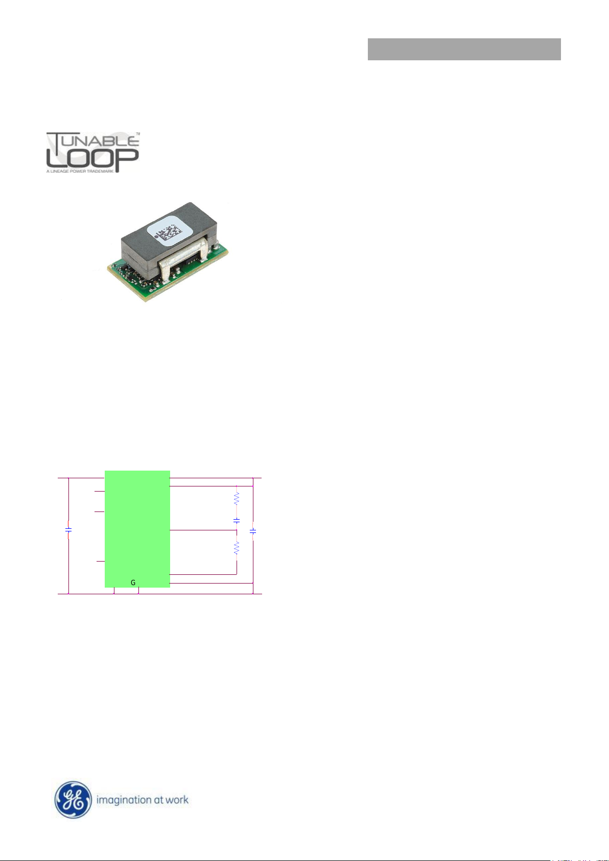
Tunable Loop
TM
to optimize dynamic output voltage
response
Flexible output voltage sequencing EZ-SEQUENCE
Power Good signal
Fixed switching frequency with capability of external
synchronization
Output over current protection (non-latching)
Over temperature protection
Remote On/Off
Ability to sink and source current
Cost efficient open frame design
Small size: 20.32 mm x 11.43 mm x 8.5 mm (0.8 in x 0.45 in
x 0.334 in)
Wide operating temperature range [-40°C to 85°C]
UL* 60950-1 2
nd
Ed. Recognized, CSA† C22.2 No. 60950-1-
07 Certified, and VDE‡ (EN60950-1 2nd Ed.) Licensed
ISO** 9001 and ISO 14001 certified manufacturing
facilities
Applications
Distributed power architectures
Intermediate bus voltage applications
Telecommunications equipment
Servers and storage applications
Networking equipment
Industrial equipment
Description
The 20A Analog MicroDLynxTM power modules are non-isolated dc-dc converters that can deliver up to 20A of output current.
These modules operate over a wide range of input voltage (VIN = 3Vdc-14.4Vdc) and provide a precisely regulated output voltage
from 0.6Vdc to 5.5Vdc, programmable via an external resistor. Features include remote On/Off, adjustable output voltage, over
current and over temperature protection. The module also includes the Tunable LoopTM feature that allows the user to optimize the
dynamic response of the converter to match the load with reduced amount of output capacitance leading to savings on cost and
PWB area.
* UL is a registered trademark of Underwriters Laboratories, Inc.
†
CSA is a registered trademark of Canadian Standards Association.
‡
VDE is a trademark of Verband Deutscher Elektrotechniker e.V.
** ISO is a registered trademark of the International Organization of Standards
TRIM
VOUT
VS+
GND
RTUNE
CTUNE
RTrim
VIN
Co
Cin
Vout+
Vin+
ON/OFF
SEQ
MODULE
PGOOD
SIG_GND
VS-
GND
SYNC
RoHS Compliant
20A Analog MicroDLynxTM: Non-Isolated DC-DC Power Modules
3Vdc –14.4Vdc input; 0.45Vdc to 5.5Vdc output; 20A Output Current
Page 2
GE
Data Sheet
20A Analog MicroDLynxTM: Non-Isolated DC-DC Power Modules
3Vdc –14.4Vdc input; 0.45Vdc to 5.5Vdc output; 20A Output Current
April 24, 2013
©2012 General Electric Company. All rights reserved.
Page 2
Parameter
Device
Symbol
Min
Max
Unit
Input Voltage
All
V
IN
-0.3
15
V
Continuous
SEQ, SYNC, VS+
All 7 V
Operating Ambient Temperature
All
TA -40
85
°C
(see Thermal Considerations section)
Storage Temperature
All
T
stg
-55
125
°C
Parameter
Device
Symbol
Min
Typ
Max
Unit
Operating Input Voltage
All
VIN
3 14.4
Vdc
Maximum Input Current
All
I
IN,max
19
Adc
(VIN=3V to 14V, IO=I
O, max
)
Input No Load Current
(VIN = 12Vdc, IO = 0, module enabled)
V
O,set
= 0.6
Vdc
I
IN,No load
69 mA
V
O,set
=
5Vdc
I
IN,No load
134 mA
Input Stand-by Current
(VIN = 12Vdc, module disabled)
All
I
IN,stand-by
16.4 mA
Inrush Transient
All
I2t
1
A2s
Input Reflected Ripple Current, peak-to-peak
(5Hz to 20MHz, 1μH source impedance; VIN =0 to 14V, IO= I
Omax
;
See Test Configurations)
All
50 mAp-p
Input Ripple Rejection (120Hz)
All
-64 dB
Absolute Maximum Ratings
Stresses in excess of the absolute maximum ratings can cause permanent damage to the device. These are absolute stress ratings
only, functional operation of the device is not implied at these or any other conditions in excess of those given in the operations
sections of the data sheet. Exposure to absolute maximum ratings for extended periods can adversely affect the device reliability.
Electrical Specifications
Unless otherwise indicated, specifications apply over all operating input voltage, resistive load, and temperature conditions.
Page 3
GE
Data Sheet
20A Analog MicroDLynxTM: Non-Isolated DC-DC Power Modules
3Vdc –14.4Vdc input; 0.45Vdc to 5.5Vdc output; 20A Output Current
April 24, 2013
©2012 General Electric Company. All rights reserved.
Page 3
Parameter
Device
Symbol
Min
Typ
Max
Unit
Output Voltage Set-point (with 0.1% tolerance for external
resistor used to set output voltage)
All
V
O, set
-1.0 +1.0
% V
O, set
Output Voltage (Over all operating input voltage, resistive
load, and temperature conditions until end of life)
All
V
O, set
-3.0 +3.0
% V
O, set
Adjustment Range (selected by an external resistor)
(Some output voltages may not be possible depending on the
input voltage – see Feature Descriptions Section)
All
VO 0.6 5.5
Vdc
Remote Sense Range
All
0.5
Vdc
Output Regulation (for VO ≥ 2.5Vdc)
Line (VIN=V
IN, min
to V
IN, max
)
All
+0.4
% V
O, set
Load (IO=I
O, min
to I
O, max
)
All
10
mV
Output Regulation (for VO < 2.5Vdc)
Line (VIN=V
IN, min
to V
IN, max
)
All
5
mV
Load (IO=I
O, min
to I
O, max
)
All
10
mV
Temperature (T
ref=TA, min
to T
A, max
)
All
0.4
% V
O, set
Output Ripple and Noise on nominal output
(VIN=V
IN, nom
and IO=I
O, min
to I
O, max
Co = 0.1μF // 22 μF ceramic
capacitors)
Peak-to-Peak (5Hz to 20MHz bandwidth)
All
50
100
mV
pk-pk
RMS (5Hz to 20MHz bandwidth)
All
20
38
mV
rms
External Capacitance1
Without the Tunable Loop
TM
ESR ≥ 1 mΩ
All
C
O, max
2x47 2x47
μF
With the Tunable Loop
TM
ESR ≥ 0.15 mΩ
All
C
O, max
2x47 1000
μF
ESR ≥ 10 mΩ
All
C
O, max
2x47
10000
μF
Output Current (in either sink or source mode)
All
Io 0 20
Adc
Output Current Limit Inception (Hiccup Mode)
(current limit does not operate in sink mode)
All
I
O, lim
130 % I
o,max
Output Short-Circuit Current
All
I
O, s/c
1.4 Arms
(VO≤250mV) ( Hiccup Mode )
Efficiency
V
O,set
= 0.6Vdc
η 79.2 %
VIN= 12Vdc, TA=25°C
V
O, set
= 1.2Vdc
η 87.1 %
IO=I
O, max , VO
= V
O,set
V
O,set
= 1.8Vdc
η 90.4 %
V
O,set
= 2.5Vdc
η 92.6 %
V
O,set
= 3.3Vdc
η 93.8 %
V
O,set
= 5.0Vdc
η 95.2 %
Switching Frequency
All
f
sw
500 kHz
Electrical Specifications (continued)
1
External capacitors may require using the new Tunable LoopTM feature to ensure that the module is stable as well as getting the best
transient response. See the Tunable LoopTM section for details.
Page 4
GE
Data Sheet
20A Analog MicroDLynxTM: Non-Isolated DC-DC Power Modules
3Vdc –14.4Vdc input; 0.45Vdc to 5.5Vdc output; 20A Output Current
April 24, 2013
©2012 General Electric Company. All rights reserved.
Page 4
Parameter
Device
Symbol
Min
Typ
Max
Unit
Frequency Synchronization
All
Synchronization Frequency Range
All
425 600
kHz
High-Level Input Voltage
All
V
IH
2.0
V
Low-Level Input Voltage
All
V
IL
0.4 V Input Current, SYNC
All
I
SYNC
100
nA
Minimum Pulse Width, SYNC
All
t
SYNC
100
ns
Maximum SYNC rise time
All
t
SYNC_SH
100
ns
Parameter
Device
Min
Typ
Max
Unit
Calculated MTBF (IO=0.8I
O, max
, TA=40°C) Telecordia Issue 2
Method 1 Case 3
All
15,45
5,614
Hours
Weight
4.54
(0.16)
g (oz.)
Parameter
Device
Symbol
Min
Typ
Max
Unit
On/Off Signal Interface
(VIN=V
IN, min
to V
IN, max
; open collector or equivalent,
Signal referenced to GND)
Device code with suffix “4” – Positive Logic (See Ordering
Information)
Logic High (Module ON)
Input High Current
All
IIH 1
mA
Input High Voltage
All
VIH 2 V
IN,max
V
Logic Low (Module OFF)
Input Low Current
All
IIL
1
mA
Input Low Voltage
All
VIL -0.2 0.6
V
Device Code with no suffix – Negative Logic (See Ordering
Information)
(On/OFF pin is open collector/drain logic input with
external pull-up resistor; signal referenced to GND)
Logic High (Module OFF)
Input High Current
All
IIH ― ― 1 mA
Input High Voltage
All
VIH 2 ―
V
IN, max
Vdc
Logic Low (Module ON)
Input low Current
All
IIL ― ―
10
μA
Input Low Voltage
All
VIL
-0.2 ― 0.6
Vdc
Electrical Specifications (continued)
General Specifications
Feature Specifications
Unless otherwise indicated, specifications apply overall operating input voltage, resistive load, and temperature conditions. See
Feature Descriptions for additional information.
Page 5
GE
Data Sheet
20A Analog MicroDLynxTM: Non-Isolated DC-DC Power Modules
3Vdc –14.4Vdc input; 0.45Vdc to 5.5Vdc output; 20A Output Current
April 24, 2013
©2012 General Electric Company. All rights reserved.
Page 5
Parameter
Device
Symbol
Min
Typ
Max
Units
Turn-On Delay and Rise Times
(VIN=V
IN, nom
, IO=I
O, max , VO
to within ±1% of steady state)
Case 1: On/Off input is enabled and then input power is
applied (delay from instant at which VIN = V
IN, min
until Vo =
10% of Vo, set)
All
Tdelay
―
1.2 ― msec
Case 2: Input power is applied for at least one second and
then the On/Off input is enabled (delay from instant at
which Von/Off is enabled until Vo = 10% of Vo, set)
All
Tdelay
―
0.8 ― msec
Output voltage Rise time (time for Vo to rise from
10% of Vo, set to 90% of Vo, set)
All
Trise
―
2.7 ― msec
Output voltage overshoot (TA = 25oC
VIN= V
IN, min
to V
IN, max,IO
= I
O, min
to I
O, max
)
With or without maximum external capacitance
3.0
% V
O, set
Over Temperature Protection
(See Thermal Considerations section)
All
T
ref
120
°C
Tracking Accuracy (Power-Up: 2V/ms)
All
VSEQ –Vo
100
mV
(Power-Down: 2V/ms)
All
VSEQ –Vo
100
mV
(V
IN, min
to V
IN, max
; I
O, min
to I
O, max
VSEQ < Vo)
Input Undervoltage Lockout
Turn-on Threshold
All
3.25
Vdc
Turn-off Threshold
All
2.6
Vdc
Hysteresis
All
0.25 Vdc
Resolution of Adjustable Input Under Voltage Threshold
All
500
mV
PGOOD (Power Good)
Signal Interface Open Drain, V
supply
5VDC
Overvoltage threshold for PGOOD ON
All
108 %V
O, set
Overvoltage threshold for PGOOD OFF
All
105 %V
O, set
Undervoltage threshold for PGOOD ON
All
110 %V
O, set
Undervoltage threshold for PGOOD OFF
All
90 %V
O, set
Pulldown resistance of PGOOD pin
All
50 Sink current capability into PGOOD pin
All
5
mA
Feature Specifications (cont.)
* Over temperature Warning – Warning may not activate before alarm and unit may shutdown before warning
Page 6
GE
Data Sheet
20A Analog MicroDLynxTM: Non-Isolated DC-DC Power Modules
3Vdc –14.4Vdc input; 0.45Vdc to 5.5Vdc output; 20A Output Current
April 24, 2013
©2012 General Electric Company. All rights reserved.
Page 6
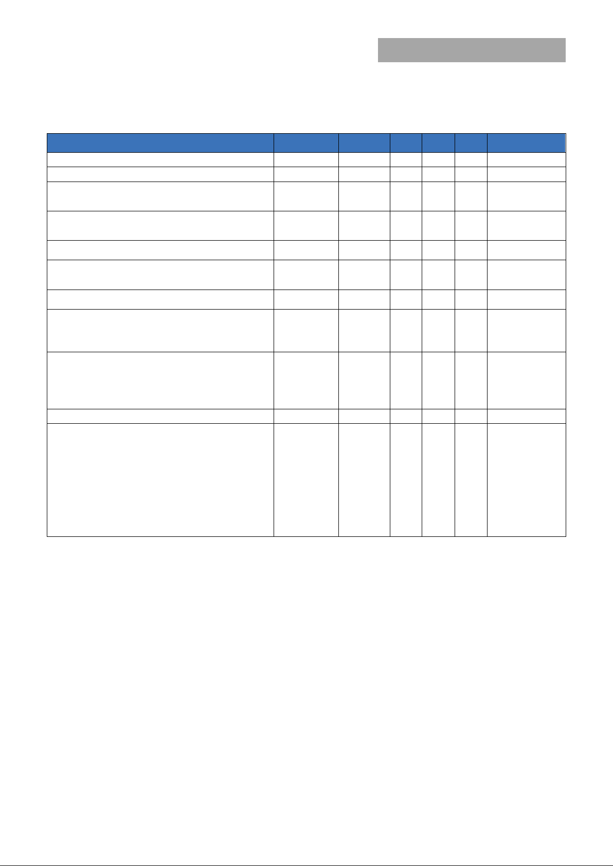
EFFICIENCY, (%)
OUTPUT CURRENT, Io (A)
OUTPUT CURRENT, IO (A)
AMBIENT TEMPERATURE, TA OC
Figure 1. Converter Efficiency versus Output Current.
Figure 2. Derating Output Current versus Ambient
Temperature and Airflow.
OUTPUT VOLTAGE
V
O
(V) (10mV/div)
OUTPUT CURRENT, OUTPUT VOLTAGE
I
O
(A) (10Adiv) V
O
(V) (10mV/div)
TIME, t (1s/div)
TIME, t (20s /div)
Figure 3. Typical output ripple and noise (CO=2x47μF
ceramic, VIN = 12V, Io = Io,max, ).
Figure 4. Transient Response to Dynamic Load Change from
50% to 100% at 12Vin, Cout= 1x47uF +11x330uF CTune=47nF,
RTune=178 ohms
OUTPUT VOLTAGE ON/OFF VOLTAGE
V
O
(V) (200mV/div) V
ON/OFF
(V) (5V/div)
OUTPUT VOLTAGE INPUT VOLTAGE
V
O
(V) (200mV/div) V
IN
(V) (5V/div)
TIME, t (2ms/div)
TIME, t (2ms/div)
Figure 5. Typical Start-up Using On/Off Voltage (Io = Io,max).
Figure 6. Typical Start-up Using Input Voltage (VIN = 12V, Io =
Io,max).
50
55
60
65
70
75
80
85
90
0 5 10 15 20
Vin=3.3V
Vin=14V
Vin=12V
2
6
10
14
18
22
55 65 75 85 95 105
0.5m/s
(100LFM)
1.5m/s
(300LFM)
1m/s
(200LFM)
NC
2m/s
(400LFM)
Characteristic Curves
The following figures provide typical characteristics for the 20A Analog MicroDLynxTM at 0.6Vo and 25oC.
Page 7
GE
Data Sheet
20A Analog MicroDLynxTM: Non-Isolated DC-DC Power Modules
3Vdc –14.4Vdc input; 0.45Vdc to 5.5Vdc output; 20A Output Current
April 24, 2013
©2012 General Electric Company. All rights reserved.
Page 7
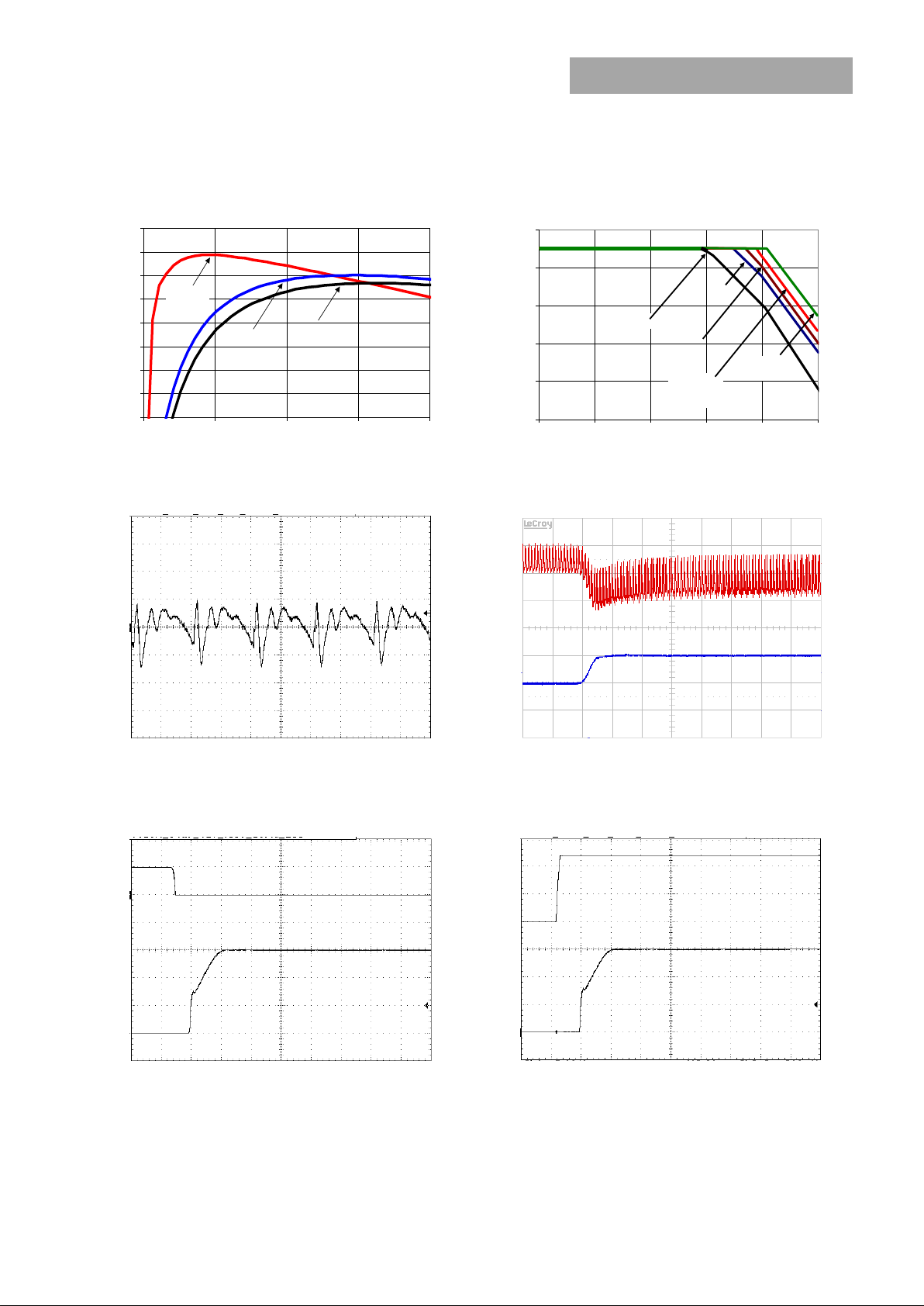
EFFICIENCY, (%)
OUTPUT CURRENT, Io (A)
OUTPUT CURRENT, IO (A)
AMBIENT TEMPERATURE, TA OC
Figure 7. Converter Efficiency versus Output Current.
Figure 8. Derating Output Current versus Ambient
Temperature and Airflow.
OUTPUT VOLTAGE
V
O
(V) (20mV/div)
OUTPUT CURRENT, OUTPUT VOLTAGE
I
O
(A) (10Adiv) V
O
(V) (20mV/div)
TIME, t (1s/div)
TIME, t (20s /div)
Figure 9. Typical output ripple and noise (CO=2x47μF
ceramic, VIN = 12V, Io = Io,max, ).
Figure 10. Transient Response to Dynamic Load Change from
50% to 100% at 12Vin, Cout= 1x47uF +5x330uF, CTune=10nF
& RTune=178 ohms
OUTPUT VOLTAGE ON/OFF VOLTAGE
V
O
(V) (500mV/div) V
ON/OFF
(V) (5V/div)
OUTPUT VOLTAGE INPUT VOLTAGE
V
O
(V) (500mV/div) V
IN
(V) (5V/div)
TIME, t (2ms/div)
TIME, t (2ms/div)
Figure 1. Typical Start-up Using On/Off Voltage (Io = Io,max).
Figure 12. Typical Start-up Using Input Voltage (VIN = 12V, Io =
Io,max).
50
55
60
65
70
75
80
85
90
95
0 5 10 15 20
Vin=3.3V
Vin=14V
Vin=12V
2
6
10
14
18
22
55 65 75 85 95 105
2m/s
(400LFM)
1.5m/s
(300LFM)
1m/s
(200LFM)
0.5m/s
(100LFM)
NC
Characteristic Curves
The following figures provide typical characteristics for the 20A Analogl MicroDLynxTM at 1.2Vo and 25oC.
Page 8
GE
Data Sheet
20A Analog MicroDLynxTM: Non-Isolated DC-DC Power Modules
3Vdc –14.4Vdc input; 0.45Vdc to 5.5Vdc output; 20A Output Current
April 24, 2013
©2012 General Electric Company. All rights reserved.
Page 8
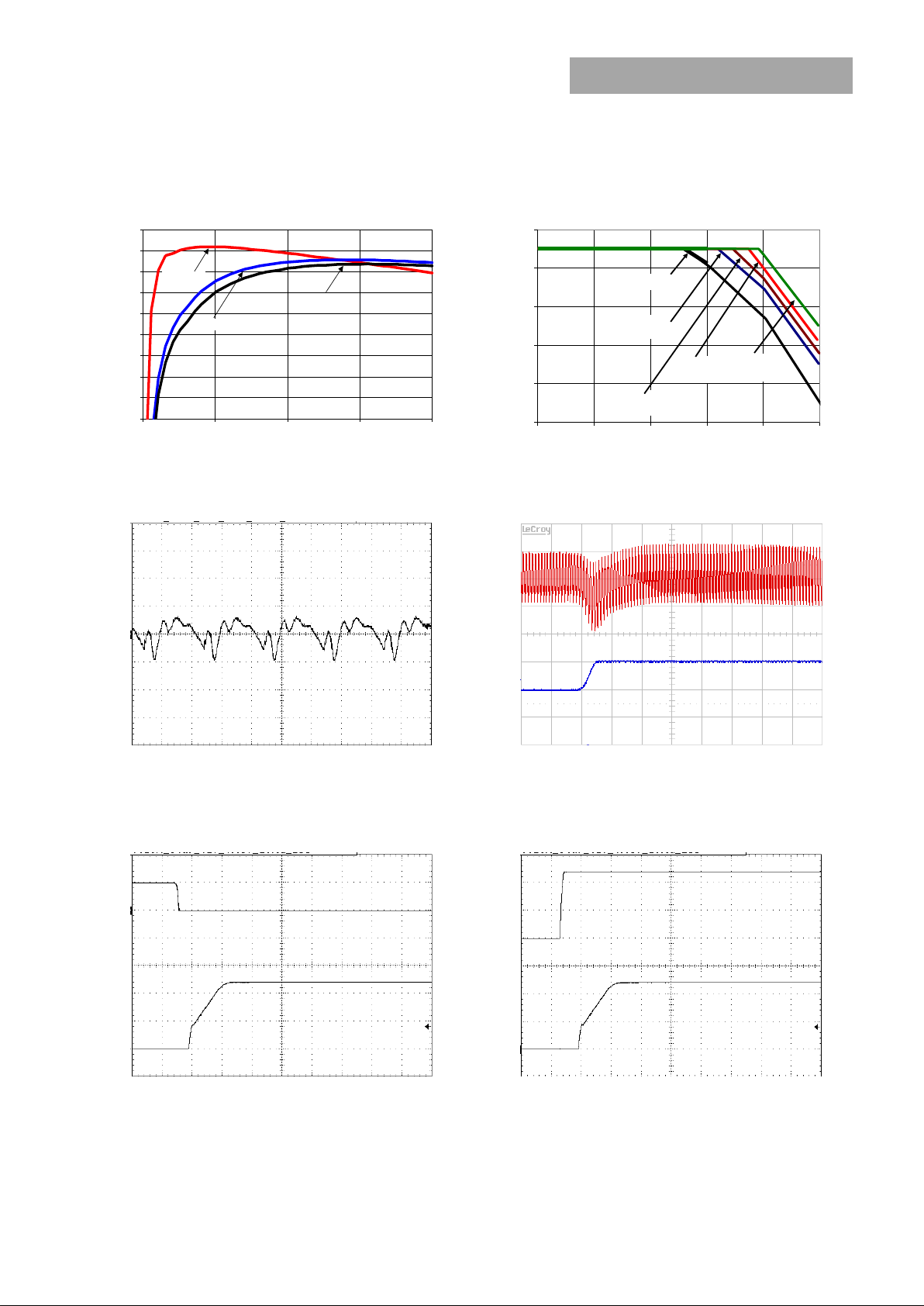
EFFICIENCY, (%)
OUTPUT CURRENT, Io (A)
OUTPUT CURRENT, IO (A)
AMBIENT TEMPERATURE, TA OC
Figure 13. Converter Efficiency versus Output Current.
Figure 14. Derating Output Current versus Ambient
Temperature and Airflow.
OUTPUT VOLTAGE
V
O
(V) (20mV/div)
OUTPUT CURRENT, OUTPUT VOLTAGE
I
O
(A) (10Adiv) V
O
(V) (20mV/div)
TIME, t (1s/div)
TIME, t (20s /div)
Figure 15. Typical output ripple and noise (CO=2X47μF
ceramic, VIN = 12V, Io = Io,max, ).
Figure 16. Transient Response to Dynamic Load Change from
50% to 100% at 12Vin, Cout= 2x47uF +3x330uF,
CTune=5600pF & RTune=220 ohms
OUTPUT VOLTAGE ON/OFF VOLTAGE
V
O
(V) (500mV/div) V
ON/OFF
(V) (5V/div)
OUTPUT VOLTAGE INPUT VOLTAGE
V
O
(V) (500mV/div) V
IN
(V) (5V/div)
TIME, t (2ms/div)
TIME, t (2ms/div)
Figure 17. Typical Start-up Using On/Off Voltage (Io = Io,max).
Figure 18. Typical Start-up Using Input Voltage (VIN = 12V, Io =
Io,max).
70
75
80
85
90
95
0 5 10 15 20
Vin=3.3V
Vin=14V
Vin=12V
2
6
10
14
18
22
55 65 75 85 95 105
2m/s
(400LFM)
1.5m/s
(300LFM)
1m/s
(200LFM)
0.5m/s
(100LFM)
NC
Characteristic Curves
The following figures provide typical characteristics for the 20A Analog MicroDLynxTM at 1.8Vo and 25oC.
Page 9

GE
Data Sheet
20A Analog MicroDLynxTM: Non-Isolated DC-DC Power Modules
3Vdc –14.4Vdc input; 0.45Vdc to 5.5Vdc output; 20A Output Current
April 24, 2013
©2012 General Electric Company. All rights reserved.
Page 9
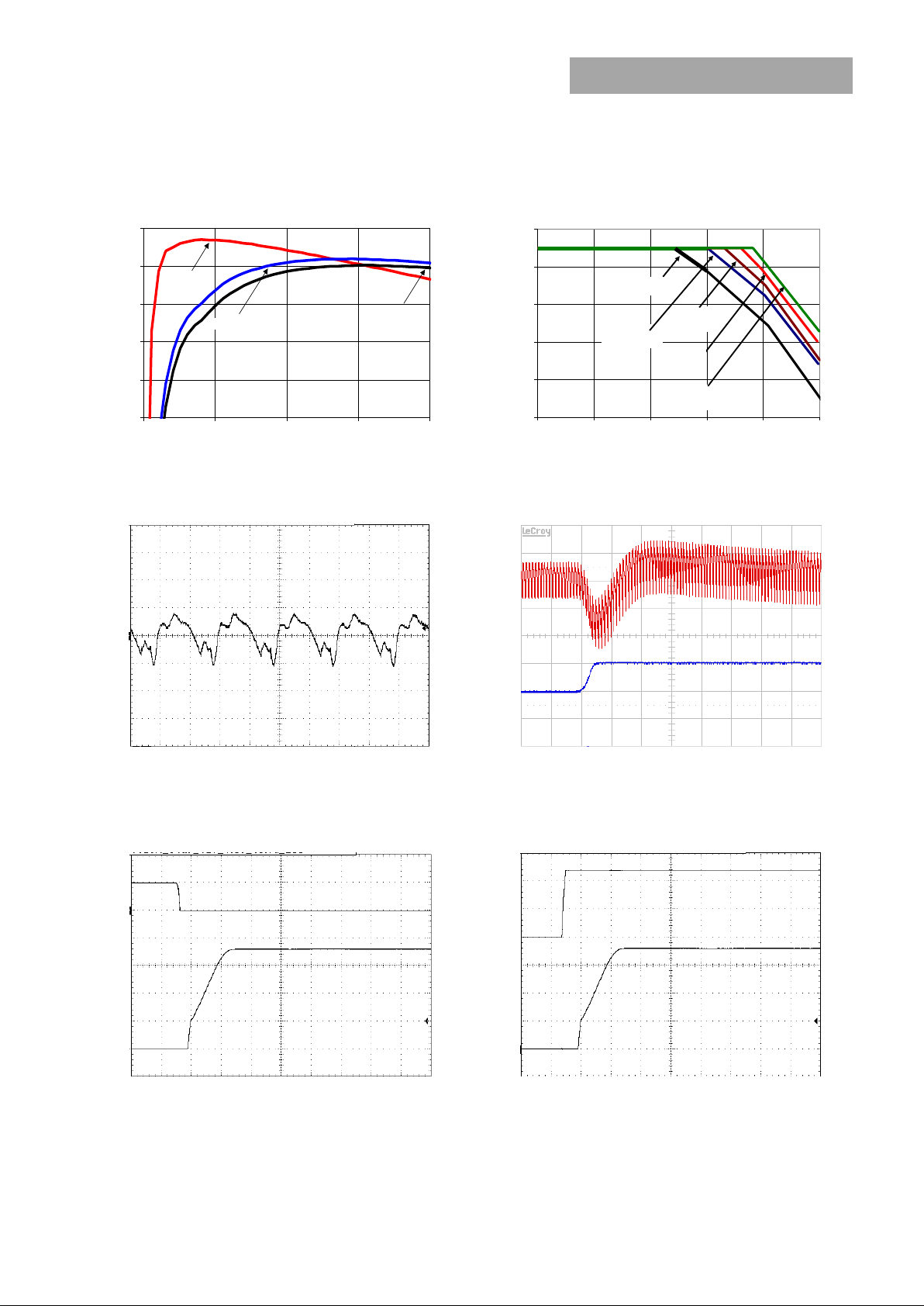
EFFICIENCY, (%)
OUTPUT CURRENT, Io (A)
OUTPUT CURRENT, IO (A)
AMBIENT TEMPERATURE, TA OC
Figure 19. Converter Efficiency versus Output Current.
Figure 20. Derating Output Current versus Ambient
Temperature and Airflow.
OUTPUT VOLTAGE
V
O
(V) (20mV/div)
OUTPUT CURRENT, OUTPUT VOLTAGE
I
O
(A) (10Adiv) V
O
(V) (20mV/div)
TIME, t (1s/div)
TIME, t (20s /div)
Figure 21. Typical output ripple and noise (CO=2x47μF
ceramic, VIN = 12V, Io = Io,max, ).
Figure 22. Transient Response to Dynamic Load Change from
50% to 100% at 12Vin, Cout= 2x47uF +2x330uF,
CTune=3300pF & RTune=220 ohms
OUTPUT VOLTAGE ON/OFF VOLTAGE
V
O
(V) (1V/div) V
ON/OFF
(V) (5V/div)
OUTPUT VOLTAGE INPUT VOLTAGE
V
O
(V) (1V/div) V
IN
(V) (5V/div)
TIME, t (2ms/div)
TIME, t (2ms/div)
Figure 23. Typical Start-up Using On/Off Voltage (Io = Io,max).
Figure 24. Typical Start-up Using Input Voltage (VIN = 12V, Io =
Io,max).
70
75
80
85
90
95
100
0 5 10 15 20
Vin=4.5V
Vin=14V
Vin=12V
2
6
10
14
18
22
55 65 75 85 95 105
2m/s
(400LFM)
1.5m/s
(300LFM)
1m/s
(200LFM)
0.5m/s
(100LFM)
NC
Characteristic Curves
The following figures provide typical characteristics for the 20A Analog MicroDLynxTM at 2.5Vo and 25oC.
Page 10

GE
Data Sheet
20A Analog MicroDLynxTM: Non-Isolated DC-DC Power Modules
3Vdc –14.4Vdc input; 0.45Vdc to 5.5Vdc output; 20A Output Current
April 24, 2013
©2012 General Electric Company. All rights reserved.
Page 10
EFFICIENCY, (%)
OUTPUT CURRENT, Io (A)
OUTPUT CURRENT, IO (A)
AMBIENT TEMPERATURE, TA OC
Figure 25. Converter Efficiency versus Output Current.
Figure 26. Derating Output Current versus Ambient
Temperature and Airflow.
OUTPUT VOLTAGE
V
O
(V) (50mV/div)
OUTPUT CURRENT, OUTPUT VOLTAGE
I
O
(A) (10Adiv) V
O
(V) (50mV/div)
TIME, t (1s/div)
TIME, t (20s /div)
Figure 27. Typical output ripple and noise (CO=2x47μF
ceramic, VIN = 12V, Io = Io,max, ).
Figure 28 Transient Response to Dynamic Load Change from
50% to 100% at 12Vin, Cout= 5x47uF +1x330uF,
CTune=2200pF & RTune=220 ohms
OUTPUT VOLTAGE ON/OFF VOLTAGE
V
O
(V) (1V/div) V
ON/OFF
(V) (5V/div)
OUTPUT VOLTAGE INPUT VOLTAGE
V
O
(V) (1V/div) V
IN
(V) (5V/div)
TIME, t (2ms/div)
TIME, t (2ms/div)
Figure 29. Typical Start-up Using On/Off Voltage (Io = Io,max).
Figure 30. Typical Start-up Using Input Voltage (VIN = 12V, Io =
Io,max).
70
75
80
85
90
95
100
0 5 10 15 20
Vin=4.5V
Vin=14V
Vin=12V
2
6
10
14
18
22
55 65 75 85 95 105
2m/s
(400LFM)
1.5m/s
(300LFM)
1m/s
(200LFM)
0.5m/s
(100LFM)
NC
2m/s
(400LFM)
1.5m/s
(300LFM)
1m/s
(200LFM)
0.5m/s
(100LFM)
NC
Characteristic Curves
The following figures provide typical characteristics for the 20A Analog MicroDLynxTM at 3.3Vo and 25oC.
Page 11

GE
Data Sheet
20A Analog MicroDLynxTM: Non-Isolated DC-DC Power Modules
3Vdc –14.4Vdc input; 0.45Vdc to 5.5Vdc output; 20A Output Current
April 24, 2013
©2012 General Electric Company. All rights reserved.
Page 11
EFFICIENCY, (%)
OUTPUT CURRENT, Io (A)
OUTPUT CURRENT, IO (A)
AMBIENT TEMPERATURE, TA OC
Figure 31. Converter Efficiency versus Output Current.
Figure 32. Derating Output Current versus Ambient
Temperature and Airflow.
OUTPUT VOLTAGE
V
O
(V) (50mV/div)
OUTPUT CURRENT, OUTPUT VOLTAGE
I
O
(A) (10Adiv) V
O
(V) (50mV/div)
TIME, t (1s/div)
TIME, t (20s /div)
Figure 33. Typical output ripple and noise (CO=2x47μF
ceramic, VIN = 12V, Io = Io,max, ).
Figure 34. Transient Response to Dynamic Load Change from
50% to 100% at 12Vin, Cout= 8x47uF, CTune=1500pF &
RTune=220 ohms
OUTPUT VOLTAGE ON/OFF VOLTAGE
V
O
(V) (2V/div) V
ON/OFF
(V) (5V/div)
OUTPUT VOLTAGE INPUT VOLTAGE
V
O
(V) (2V/div) V
IN
(V) (5V/div)
TIME, t (2ms/div)
TIME, t (2ms/div)
Figure 35. Typical Start-up Using On/Off Voltage (Io = Io,max).
Figure 36. Typical Start-up Using Input Voltage (VIN = 12V, Io =
Io,max).
70
75
80
85
90
95
100
0 5 10 15 20
Vin=7V
Vin=12V
Vin=14V
2
6
10
14
18
22
55 65 75 85 95 105
2m/s
(400LFM)
1.5m/s
(300LFM)
1m/s
(200LFM)
0.5m/s
(100LFM)
NC
Characteristic Curves
The following figures provide typical characteristics for the 20A Analog MicroDLynxTM at 5Vo and 25oC.
Page 12

GE
Data Sheet
20A Analog MicroDLynxTM: Non-Isolated DC-DC Power Modules
3Vdc –14.4Vdc input; 0.45Vdc to 5.5Vdc output; 20A Output Current
April 24, 2013
©2012 General Electric Company. All rights reserved.
Page 12
Input Ripple Voltage (mVp-p)
Output Voltage (Vdc)
0
50
100
150
200
250
300
350
400
450
0.5 1 1.5 2 2.5 3 3.5 4 4.5 5
2x22uF
3x22 uF
0
10
20
30
40
50
60
70
0.5 1 1.5 2 2.5 3 3.5 4 4.5 5
Ripple (mVp-p)
Output Voltage(Volts)
2x47uF Ext Cap
4x47uF Ext Cap
6x47uF Ext Cap
8x47uF Ext Cap
Design Considerations
Input Filtering
The 20A Analog MicroDLynxTM module should be
connected to a low ac-impedance source. A highly
inductive source can affect the stability of the module. An
input capacitance must be placed directly adjacent to the
input pin of the module, to minimize input ripple voltage
and ensure module stability.
To minimize input voltage ripple, ceramic capacitors are
recommended at the input of the module. Figure 37 shows
the input ripple voltage for various output voltages at 20A
of load current with 2x22 µF or 3x22 µF ceramic capacitors
and an input of 12V.
Figure 38. Output ripple voltage for various output
voltages with external 2x47 µF, 4x47 µF or 6x47 µF
ceramic capacitors at the output (20A load). Input voltage
is 12V.
Safety Considerations
For safety agency approval the power module must be
installed in compliance with the spacing and separation
requirements of the end-use safety agency standards, i.e.,
UL 60950-1 2nd, CSA C22.2 No. 60950-1-07, DIN EN 609501:2006 + A11 (VDE0805 Teil 1 + A11):2009-11; EN 609501:2006 + A11:2009-03.
Figure 37. Input ripple voltage for various output
voltages with 2x22 µF or 3x22 µF ceramic capacitors at
the input (20A load). Input voltage is 12V.
Output Filtering
These modules are designed for low output ripple voltage
and will meet the maximum output ripple specification with
0.1 µF ceramic and 2x47 µF ceramic capacitors at the output
of the module. However, additional output filtering may be
required by the system designer for a number of reasons.
First, there may be a need to further reduce the output ripple
and noise of the module. Second, the dynamic response
characteristics may need to be customized to a particular
load step change.
To reduce the output ripple and improve the dynamic
response to a step load change, additional capacitance at
the output can be used. Low ESR polymer and ceramic
capacitors are recommended to improve the dynamic
response of the module. Figure 38 provides output ripple
information for different external capacitance values at
various Vo and a full load current of 20A. For stable
operation of the module, limit the capacitance to less than
the maximum output capacitance as specified in the
electrical specification table. Optimal performance of the
module can be achieved by using the Tunable LoopTM feature
described later in this data sheet.
For the converter output to be considered meeting the
requirements of safety extra-low voltage (SELV), the input
must meet SELV requirements. The power module has
extra-low voltage (ELV) outputs when all inputs are ELV.
The UDT020A0X series were tested using an external
Littelfuse 456 series fast-acting fuse rated at 30 A, 100 Vdc
in the ungrounded input.
Page 13

GE
Data Sheet
20A Analog MicroDLynxTM: Non-Isolated DC-DC Power Modules
3Vdc –14.4Vdc input; 0.45Vdc to 5.5Vdc output; 20A Output Current
April 24, 2013
©2012 General Electric Company. All rights reserved.
Page 13
V
O
(+)
TRIM
VS─
R
trim
LOAD
V
IN
(+)
ON/OFF
VS+
SIG_GND
20K
Rpullup
I
20K
ON/OFF
+
20K
3.3V
470
VIN
20K
Q7
20K
100pF
4.7K
ENABLE
100K
DLYNX MODULE
47K
Q2
+VIN
20K
GND
20K
20K
2K
ON/OFF
Q6
Q5
V
Q3
_
ENABLE
470
4.7K
+VIN
20K
100K
2K
100pF
_
47K
GND
Q6
20K
Q2
+
DLYNX MODULE
V
Rpullup
Q3
ON/OFF
20K
I
ON/OFF
3.3V
Q5
20K
0
2
4
6
8
10
12
14
16
0.5 1 1.5 2 2.5 3 3.5 4 4.5 5 5.5 6
Input Voltage (v)
Output Voltage (V)
Lower
Upper
Analog Feature Descriptions
Remote On/Off
The 20A Analog MicroDLynxTM power modules feature an
On/Off pin for remote On/Off operation. Two On/Off logic
options are available. In the Positive Logic On/Off option,
(device code suffix “4” – see Ordering Information), the
module turns ON during a logic High on the On/Off pin and
turns OFF during a logic Low. With the Negative Logic On/Off
option, (no device code suffix, see Ordering Information), the
module turns OFF during logic High and ON during logic Low.
The On/Off signal should be always referenced to ground. For
either On/Off logic option, leaving the On/Off pin
disconnected will turn the module ON when input voltage is
present.
For positive logic modules, the circuit configuration for using
the On/Off pin is shown in Figure 39. When the external
transistor Q2 is in the OFF state, the internal transistor Q7 is
turned ON, which turn Q3 OFF which keeps Q6 OFF and Q5
OFF. This allows the internal PWM #Enable signal to be pulled
up by the internal 3.3V, thus turning the module ON. When
transistor Q2 is turned ON, the On/Off pin is pulled low, which
turns Q7 OFF which turns Q3, Q6 and Q5 ON and the internal
PWM #Enable signal is pulled low and the module is OFF. A
suggested value for R
For negative logic On/Off modules, the circuit configuration is
shown in Fig. 40. The On/Off pin should be pulled high with an
external pull-up resistor (suggested value for the 3V to 14V
input range is 20Kohms). When transistor Q2 is in the OFF
state, the On/Off pin is pulled high, transistor Q3 is turned ON.
This turns Q6 ON, followed by Q5 turning ON which pulls the
internal ENABLE low and the module is OFF. To turn the
module ON, Q2 is turned ON pulling the On/Off pin low,
turning transistor Q3 OFF, which keeps Q6 and Q5 OFF
resulting in the PWM Enable pin going high.
pullup
is 20k.
Monotonic Start-up and Shutdown
The module has monotonic start-up and shutdown behavior
for any combination of rated input voltage, output current
and operating temperature range.
Startup into Pre-biased Output
The module can start into a prebiased output as long as the
prebias voltage is 0.5V less than the set output voltage.
Analog Output Voltage Programming
The output voltage of the module is programmable to any
voltage from 0.6dc to 5.5Vdc by connecting a resistor
between the Trim and SIG_GND pins of the module. Certain
restrictions apply on the output voltage set point depending
on the input voltage. These are shown in the Output Voltage
vs. Input Voltage Set Point Area plot in Fig. 41. The Upper
Limit curve shows that for output voltages lower than 1V,
the input voltage must be lower than the maximum of
14.4V. The Lower Limit curve shows that for output voltages
higher than 0.6V, the input voltage needs to be larger than
the minimum of 3V. .
Figure 41. Output Voltage vs. Input Voltage Set Point Area
plot showing limits where the output voltage can be set
for different input voltages.
Figure 39. Circuit configuration for using positive On/Off
logic.
Figure 40. Circuit configuration for using negative On/Off
logic.
Caution – Do not connect SIG_GND to GND elsewhere in the
layout
Figure 42. Circuit configuration for programming output
voltage using an external resistor.
Page 14

GE
Data Sheet
20A Analog MicroDLynxTM: Non-Isolated DC-DC Power Modules
3Vdc –14.4Vdc input; 0.45Vdc to 5.5Vdc output; 20A Output Current
April 24, 2013
©2012 General Electric Company. All rights reserved.
Page 14
k
Vo
Rtrim
6.0
12
V
O, set
(V)
Rtrim (KΩ)
0.6
Open
0.9
40
1.0
30
1.2
20
1.5
13.33
1.8
10
2.5
6.316
3.3
4.444
5.0
2.727
100 pF
DLynx Module
R1=Rtrim
20K
SIG_GND
SEQ
SEQ
V
Vo
MODULE
SIG_GND
Trim
Q1
Rtrim
Rmargin-up
Q2
Rmargin-down
Without an external resistor between Trim and SIG_GND pins,
the output of the module will be 0.6Vdc. To calculate the
value of the trim resistor, Rtrim for a desired output voltage,
should be as per the following equation:
Rtrim is the external resistor in kΩ
Vo is the desired output voltage.
Table 1 provides Rtrim values required for some common
output voltages.
Table 1
Remote Sense
The power module has a Remote Sense feature to minimize
the effects of distribution losses by regulating the voltage
between the sense pins (VS+ and VS-). The voltage drop
between the sense pins and the VOUT and GND pins of the
module should not exceed 0.5V.
Analog Voltage Margining
Output voltage margining can be implemented in the module
by connecting a resistor, R
ground pin for margining-up the output voltage and by
connecting a resistor, R
pin for margining-down. Figure 43 shows the circuit
configuration for output voltage margining. The POL
Programming Tool, available at www.lineagepower.com
under the Downloads section, also calculates the values of
R
margin. Please consult your local Lineage Power technical
representative for additional details.
margin-up
and R
margin-down
margin-down
for a specific output voltage and %
, from the Trim pin to the
margin-up
, from the Trim pin to output
Figure 43. Circuit Configuration for margining Output
voltage.
Output Voltage Sequencing
The power module includes a sequencing feature, EZSEQUENCE that enables users to implement various types of
output voltage sequencing in their applications. This is
accomplished via an additional sequencing pin. When not
using the sequencing feature, leave it unconnected.
The voltage applied to the SEQ pin should be scaled down
by the same ratio as used to scale the output voltage down
to the reference voltage of the module. This is accomplished
by an external resistive divider connected across the
sequencing voltage before it is fed to the SEQ pin as shown
in Fig. 44. In addition, a small capacitor (suggested value
100pF) should be connected across the lower resistor R1.
For all DLynx modules, the minimum recommended delay
between the ON/OFF signal and the sequencing signal is
10ms to ensure that the module output is ramped up
according to the sequencing signal. This ensures that the
module soft-start routine is completed before the
sequencing signal is allowed to ramp up.
Figure 44. Circuit showing connection of the sequencing
signal to the SEQ pin.
When the scaled down sequencing voltage is applied to the
SEQ pin, the output voltage tracks this voltage until the
output reaches the set-point voltage. The final value of the
sequencing voltage must be set higher than the set-point
voltage of the module. The output voltage follows the
sequencing voltage on a one-to-one basis. By connecting
Page 15

GE
Data Sheet
20A Analog MicroDLynxTM: Non-Isolated DC-DC Power Modules
3Vdc –14.4Vdc input; 0.45Vdc to 5.5Vdc output; 20A Output Current
April 24, 2013
©2012 General Electric Company. All rights reserved.
Page 15
MODULE
SYNC
GND
+
─
multiple modules together, multiple modules can track their
output voltages to the voltage applied on the SEQ pin.
To initiate simultaneous shutdown of the modules, the SEQ
pin voltage is lowered in a controlled manner. The output
voltage of the modules tracks the voltages below their setpoint voltages on a one-to-one basis. A valid input voltage
must be maintained until the tracking and output voltages
reach ground potential.
Overcurrent Protection
To provide protection in a fault (output overload) condition,
the unit is equipped with internal current-limiting circuitry
and can endure current limiting continuously. At the point of
current-limit inception, the unit enters hiccup mode. The unit
operates normally once the output current is brought back
into its specified range.
Overtemperature Protection
To provide protection in a fault condition, the unit is equipped
with a thermal shutdown circuit. The unit will shut down if the
overtemperature threshold of 120oC(typ) is exceeded at the
thermal reference point T
shutdown it will then wait to cool before attempting to
restart.
.Once the unit goes into thermal
ref
Input Undervoltage Lockout
At input voltages below the input undervoltage lockout limit,
the module operation is disabled. The module will begin to
operate at an input voltage above the undervoltage lockout
turn-on threshold.
Synchronization
The module switching frequency can be synchronized to a
signal with an external frequency within a specified range.
Synchronization can be done by using the external signal
applied to the SYNC pin of the module as shown in Fig. 45,
with the converter being synchronized by the rising edge of
the external signal. The Electrical Specifications table
specifies the requirements of the external SYNC signal. If the
SYNC pin is not used, the module should free run at the
default switching frequency. If synchronization is not being
used, connect the SYNC pin to GND.
Figure 45. External source connections to synchronize
switching frequency of the module.
Dual Layout
Identical dimensions and pin layout of Analog and Digital
MicroDLynx modules permit migration from one to the other
without needing to change the layout. In both cases the trim
resistor is connected between trim and signal ground. The
output of the analog module cannot be trimmed down to
0.45V
Power Good
The module provides a Power Good (PGOOD) signal that is
implemented with an open-drain output to indicate that the
output voltage is within the regulation limits of the power
module. The PGOOD signal will be de-asserted to a low state
if any condition such as overtemperature, overcurrent or
loss of regulation occurs that would result in the output
voltage going ±10% outside the setpoint value. The PGOOD
terminal can be connected through a pullup resistor
(suggested value 100K) to a source of 5VDC or lower.
Page 16

GE
Data Sheet
20A Analog MicroDLynxTM: Non-Isolated DC-DC Power Modules
3Vdc –14.4Vdc input; 0.45Vdc to 5.5Vdc output; 20A Output Current
April 24, 2013
©2012 General Electric Company. All rights reserved.
Page 16
Co
2x47F
4x47F
6x47F
10x47F
20x47F
R
TUNE
330
330
270
220
180
C
TUNE
47pF
560pF
1200pF
2200pF
4700pF
Vo
5V
3.3V
2.5V
1.8V
1.2V
0.6V
Co
8x47F
5x47F +
1x330F
Polymer
2x47F
+
2x330F
Polymer
2x47F
+
3x330F
Polymer
1x47F
+
5x330F
Polymer
1x47F
+
11x330F
Polymer
R
TUNE
220
220
220
220
180
180
C
TUNE
1500pF
2200pF
3300pF
5600pF
10nF
47nF
V
100mV
64mV
49mV
36mV
24mV
12mV
VS+
MODULE
SIG_GND
TRIM
VOUT
RTune
CTune
RTrim
CO
GND
Tunable Loop
TM
The module has a feature that optimizes transient response
of the module called Tunable LoopTM.
External capacitors are usually added to the output of the
module for two reasons: to reduce output ripple and noise
(see Figure 38) and to reduce output voltage deviations from
the steady-state value in the presence of dynamic load
current changes. Adding external capacitance however
affects the voltage control loop of the module, typically
causing the loop to slow down with sluggish response.
Larger values of external capacitance could also cause the
module to become unstable.
The Tunable LoopTM allows the user to externally adjust the
voltage control loop to match the filter network connected to
the output of the module. The Tunable LoopTM is implemented
by connecting a series R-C between the VS+ and TRIM pins of
the module, as shown in Fig. 46. This R-C allows the user to
externally adjust the voltage loop feedback compensation of
the module.
different values of ceramic output capacitors up to 1000uF
that might be needed for an application to meet output ripple
and noise requirements. Selecting R
TUNE
and C
according
TUNE
to Table 3 will ensure stable operation of the module.
In applications with tight output voltage limits in the presence
of dynamic current loading, additional output capacitance
will be required. Table 3 lists recommended values of R
and C
in order to meet 2% output voltage deviation limits
TUNE
TUNE
for some common output voltages in the presence of a 10A
to 20A step change (50% of full load), with an input voltage of
12V.
Please contact your Lineage Power technical representative
to obtain more details of this feature as well as for guidelines
on how to select the right value of external R-C to tune the
module for best transient performance and stable operation
for other output capacitance values.
Table 2. General recommended values of of R
C
for Vin=12V and various external ceramic capacitor
TUNE
TUNE
and
combinations.
Table 3. Recommended values of R
TUNE
and C
TUNE
to obtain
transient deviation of 2% of Vout for a 10A step load with
Vin=12V.
Figure. 46. Circuit diagram showing connection of R
and C
Recommended values of R
capacitor combinations are given in Tables 2 and 3. Table 3
shows the recommended values of R
to tune the control loop of the module.
TUNE
and C
TUNE
for different output
TUNE
TUNE
and C
TUNE
for
TUME
Note: The capacitors used in the Tunable Loop tables are
47 μF/3 mΩ ESR ceramic and 330 μF/12 mΩ ESR polymer
capacitors.
Page 17

GE
Data Sheet
20A Analog MicroDLynxTM: Non-Isolated DC-DC Power Modules
3Vdc –14.4Vdc input; 0.45Vdc to 5.5Vdc output; 20A Output Current
April 24, 2013
©2012 General Electric Company. All rights reserved.
Page 17
Air
flow
x
Power Module
Wind Tunnel
PWBs
12.7_
(0.50)
76.2_
(3.0)
Probe Location
for measuring
airflow and
ambient
temperature
25.4_
(1.0)
Figure 48. Thermal Test Setup.
Thermal Considerations
Power modules operate in a variety of thermal environments;
however, sufficient cooling should always be provided to help
ensure reliable operation.
Considerations include ambient temperature, airflow, module
power dissipation, and the need for increased reliability. A
reduction in the operating temperature of the module will
result in an increase in reliability. The thermal data presented
here is based on physical measurements taken in a wind
tunnel. The test set-up is shown in Figure 48. The preferred
airflow direction for the module is in Figure 49.
The thermal reference points, T
used in the specifications
ref
are also shown in Figure 49. For reliable operation the
temperatures at these points should not exceed 130oC. The
output power of the module should not exceed the rated
power of the module (Vo,set x Io,max).
Please refer to the Application Note “Thermal
Characterization Process For Open-Frame Board-Mounted
Power Modules” for a detailed discussion of thermal
aspects including maximum device temperatures.
Figure 49. Preferred airflow direction and location of hotspot of the module (Tref).
Page 18

GE
Data Sheet
20A Analog MicroDLynxTM: Non-Isolated DC-DC Power Modules
3Vdc –14.4Vdc input; 0.45Vdc to 5.5Vdc output; 20A Output Current
April 24, 2013
©2012 General Electric Company. All rights reserved.
Page 18
Frequency (Hz)
PSD Level
(G2/Hz)
Frequency (Hz)
PSD Level
(G2/Hz)
Frequency (Hz)
PSD Level
(G2/Hz)
10
1.14E-03
170
2.54E-03
690
1.03E-03
30
5.96E-03
230
3.70E-03
800
7.29E-03
40
9.53E-04
290
7.99E-04
890
1.00E-03
50
2.08E-03
340
1.12E-02
1070
2.67E-03
90
2.08E-03
370
1.12E-02
1240
1.08E-03
110
7.05E-04
430
8.84E-04
1550
2.54E-03
130
5.00E-03
490
1.54E-03
1780
2.88E-03
140
8.20E-04
560
5.62E-04
2000
5.62E-04
Frequency (Hz)
PSD Level
(G2/Hz)
Frequency (Hz)
PSD Level
(G2/Hz)
Frequency (Hz)
PSD Level
(G2/Hz)
10
0.00803
170
0.01795
690
0.00727
30
0.04216
230
0.02616
800
0.05155
40
0.00674
290
0.00565
890
0.00709
50
0.01468
340
0.07901
1070
0.01887
90
0.01468
370
0.07901
1240
0.00764
110
0.00498
430
0.00625
1550
0.01795
130
0.03536
490
0.01086
1780
0.02035
140
0.0058
560
0.00398
2000
0.00398
Shock and Vibration
The ruggedized (-D version) of the modules are designed to
withstand elevated levels of shock and vibration to be able to
operate in harsh environments. The ruggedized modules
have been successfully tested to the following conditions:
Non operating random vibration:
Random vibration tests conducted at 25C, 10 to 2000Hz, for
30 minutes each level, starting from 30Grms (Z axis) and up to
50Grms (Z axis). The units were then subjected to two more
tests of 50Grms at 30 minutes each for a total of 90 minutes.
Operating shock to 40G per Mil Std. 810F, Method 516.4
Procedure I:
The modules were tested in opposing directions along each
of three orthogonal axes, with waveform and amplitude of
the shock impulse characteristics as follows:
All shocks were half sine pulses, 11 milliseconds (ms) in
duration in all 3 axes.
Units were tested to the Functional Shock Test of MIL-STD810, Method 516.4, Procedure I - Figure 516.4-4. A shock
magnitude of 40G was utilized. The operational units were
Table 7: Performance Vibration Qualification - All Axes
subjected to three shocks in each direction along three axes
for a total of eighteen shocks.
Operating vibration per Mil Std 810F, Method 514.5
Procedure I:
The ruggedized (-D version) modules are designed and
tested to vibration levels as outlined in MIL-STD-810F,
Method 514.5, and Procedure 1, using the Power Spectral
Density (PSD) profiles as shown in Table 7 and Table 8 for all
axes. Full compliance with performance specifications was
required during the performance test. No damage was
allowed to the module and full compliance to performance
specifications was required when the endurance
environment was removed. The module was tested per MILSTD-810, Method 514.5, Procedure I, for functional
(performance) and endurance random vibration using the
performance and endurance levels shown in Table 7 and
Table 8 for all axes. The performance test has been split,
with one half accomplished before the endurance test and
one half after the endurance test (in each axis). The duration
of the performance test was at least 16 minutes total per
axis and at least 120 minutes total per axis for the
endurance test. The endurance test period was 2 hours
minimum per axis.
Table 8: Endurance Vibration Qualification - All Axes
Page 19

GE
Data Sheet
20A Analog MicroDLynxTM: Non-Isolated DC-DC Power Modules
3Vdc –14.4Vdc input; 0.45Vdc to 5.5Vdc output; 20A Output Current
April 24, 2013
©2012 General Electric Company. All rights reserved.
Page 19
VS-
GND
Vin+
CI3
CO3
VOUT
VS+
GND
TRIM
CTUNE
RTUNE
RTrim
VIN
CO1
CI1
Vout+
ON/OFF
SEQ
MODULE
PGOOD
SIG_GND
SYNC
CI2
CO2
Example Application Circuit
Requirements:
Vin: 12V
Vout: 1.8V
Iout: 15A max., worst case load transient is from 10A to 15A
Vout: 1.5% of Vout (27mV) for worst case load transient
Vin, ripple 1.5% of Vin (180mV, p-p)
CI1 Decoupling cap - 1x0.047F/16V ceramic capacitor (e.g. Murata LLL185R71C473MA01)
CI2 3x22F/16V ceramic capacitor (e.g. Murata GRM32ER61C226KE20)
CI3 47F/16V bulk electrolytic
CO1 Decoupling cap - 1x0.047F/16V ceramic capacitor (e.g. Murata LLL185R71C473MA01)
CO2 N.A.
CO3 3 x 330F/6.3V Polymer (e.g. Sanyo Poscap)
CTune 4700pF ceramic capacitor (can be 1206, 0805 or 0603 size)
RTune 330 ohms SMT resistor (can be 1206, 0805 or 0603 size)
RTrim 10k SMT resistor (can be 1206, 0805 or 0603 size, recommended tolerance of 0.1%)
Page 20

GE
Data Sheet
20A Analog MicroDLynxTM: Non-Isolated DC-DC Power Modules
3Vdc –14.4Vdc input; 0.45Vdc to 5.5Vdc output; 20A Output Current
April 24, 2013
©2012 General Electric Company. All rights reserved.
Page 20
PIN
FUNCTION
PIN
FUNCTION
1
ON/OFF
10
SYNC1
2
VIN
11
NC 3 SEQ
12
NC
4
GND
13
NC
5
TRIM
14
SIG_GND
6
VOUT
15
NC
7
VS+
16
NC 8 VS- 9 PG
Mechanical Outline
Dimensions are in millimeters and (inches).
Tolerances: x.x mm 0.5 mm (x.xx in. 0.02 in.) [unless otherwise indicated]
x.xx mm 0.25 mm (x.xxx in 0.010 in.)
1
If unused, connect to Ground.
Page 21

GE
Data Sheet
20A Analog MicroDLynxTM: Non-Isolated DC-DC Power Modules
3Vdc –14.4Vdc input; 0.45Vdc to 5.5Vdc output; 20A Output Current
April 24, 2013
©2012 General Electric Company. All rights reserved.
Page 21
PIN
FUNCTION
PIN
FUNCTION
1
ON/OFF
10
SYNC2
2
VIN
11
NC 3 SEQ
12
NC 4 GND
13
NC 5 TRIM
14
SIG_GND
6
VOUT
15
NC
7
VS+
16
NC 8 VS-
9
PG
Recommended Pad Layout
Dimensions are in millimeters and (inches).
Tolerances: x.x mm 0.5 mm (x.xx in. 0.02 in.) [unless otherwise indicated]
x.xx mm 0.25 mm (x.xxx in 0.010 in.)
2
If unused, connect to Ground.
Page 22

GE
Data Sheet
20A Analog MicroDLynxTM: Non-Isolated DC-DC Power Modules
3Vdc –14.4Vdc input; 0.45Vdc to 5.5Vdc output; 20A Output Current
April 24, 2013
©2012 General Electric Company. All rights reserved.
Page 22
Packaging Details
The 12V Analog MicroDLynxTM 20A modules are supplied in tape & reel as standard. Modules are shipped in quantities of 200
modules per reel.
All Dimensions are in millimeters and (in inches).
Reel Dimensions:
Outside Dimensions: 330.2 mm (13.00)
Inside Dimensions: 177.8 mm (7.00”)
Tape Width: 44.00 mm (1.732”)
Page 23

GE
Data Sheet
20A Analog MicroDLynxTM: Non-Isolated DC-DC Power Modules
3Vdc –14.4Vdc input; 0.45Vdc to 5.5Vdc output; 20A Output Current
April 24, 2013
©2012 General Electric Company. All rights reserved.
Page 23
Per J-STD-020 Rev. C
0
50
100
150
200
250
300
Reflow Time (Seconds)
Reflow Temp (°C)
Heating Zone
1°C/Second
Peak Temp 260°C
* Min. Time Above 235°C
15 Seconds
*Time Above 217°C
60 Seconds
Cooling
Zone
Surface Mount Information
Pick and Place
The 20A Analog MicroDLynxTM modules use an open frame
construction and are designed for a fully automated
assembly process. The modules are fitted with a label
designed to provide a large surface area for pick and place
operations. The label meets all the requirements for surface
mount processing, as well as safety standards, and is able to
withstand reflow temperatures of up to 300oC. The label also
carries product information such as product code, serial
number and the location of manufacture.
Nozzle Recommendations
The module weight has been kept to a minimum by using
open frame construction. Variables such as nozzle size, tip
style, vacuum pressure and placement speed should be
considered to optimize this process. The minimum
recommended inside nozzle diameter for reliable operation is
3mm. The maximum nozzle outer diameter, which will safely
fit within the allowable component spacing, is 7 mm.
Bottom Side / First Side Assembly
This module is not recommended for assembly on the bottom
side of a customer board. If such an assembly is attempted,
components may fall off the module during the second reflow
process.
Lead Free Soldering
The modules are lead-free (Pb-free) and RoHS compliant and
fully compatible in a Pb-free soldering process. Failure to
observe the instructions below may result in the failure of or
cause damage to the modules and can adversely affect longterm reliability.
Moisture barrier bags (MBB) with desiccant are required for
MSL ratings of 2 or greater. These sealed packages should
not be broken until time of use. Once the original package is
broken, the floor life of the product at conditions of 30°C
and 60% relative humidity varies according to the MSL rating
(see J-STD-033A). The shelf life for dry packed SMT packages
will be a minimum of 12 months from the bag seal date,
when stored at the following conditions: < 40° C, < 90%
relative humidity.
Figure 50. Recommended linear reflow profile using
Sn/Ag/Cu solder.
Post Solder Cleaning and Drying Considerations
Post solder cleaning is usually the final circuit-board
assembly process prior to electrical board testing. The result
of inadequate cleaning and drying can affect both the
reliability of a power module and the testability of the
finished circuit-board assembly. For guidance on
appropriate soldering, cleaning and drying procedures, refer
to Board Mounted Power Modules: Soldering and Cleaning
Application Note (AN04-001).
Pb-free Reflow Profile
Power Systems will comply with J-STD-020 Rev. C
(Moisture/Reflow Sensitivity Classification for Nonhermetic
Solid State Surface Mount Devices) for both Pb-free solder
profiles and MSL classification procedures. This standard
provides a recommended forced-air-convection reflow profile
based on the volume and thickness of the package (table 4-
2). The suggested Pb-free solder paste is Sn/Ag/Cu (SAC). For
questions regarding Land grid array(LGA) soldering, solder
volume; please contact Lineage Power for special
manufacturing process instructions. The recommended linear
reflow profile using Sn/Ag/Cu solder is shown in Fig. 50.
Soldering outside of the recommended profile requires
testing to verify results and performance.
MSL Rating
The 20A Analog MicroDLynxTM modules have a MSL rating of
2a.
Storage and Handling
The recommended storage environment and handling
procedures for moisture-sensitive surface mount packages is
detailed in J-STD-033 Rev. A (Handling, Packing, Shipping and
Use of Moisture/Reflow Sensitive Surface Mount Devices).
Page 24

GE
Data Sheet
20A Analog MicroDLynxTM: Non-Isolated DC-DC Power Modules
3Vdc –14.4Vdc input; 0.45Vdc to 5.5Vdc output; 20A Output Current
Contact Us
For more information, call us at
USA/Canada:
+1 888 546 3243, or +1 972 244 9288
Asia-Pacific:
+86.021.54279977*808
Europe, Middle-East and Africa:
+49.89.74423-206
India:
+91.80.28411633
www.ge.com/powerelectronics
April 24, 2013
©2012 General Electric Company. All rights reserved.
Version 1.26
Device Code
Input
Voltage Range
Output
Voltage
Output
Current
On/Off
Logic
Sequencing
Comcodes
UDT020A0X3-SRZ
3 – 14.4Vdc
0.45 – 5.5Vdc
20A
Negative
Yes
CC109159728
UDT020A0X3-SRDZ
3 – 14.4Vdc
0.45 – 5.5Vdc
20A
Negative
Yes
CC109168745
UDT020A0X43-SRZ
3 – 14.4Vdc
0.45 – 5.5Vdc
20A
Positive
Yes
CC109159736
Package
Identifier
Family
Sequencing
Option
Output
current
Remot
e
Sense
Options
ROHS
Compliance
U D T
020A0 X 3 -SR
-D
Z
P=Pico
U=Micro
M=Mega
G=Giga
D=Dlynx
Digital
V = DLynx
Analog.
T=with EZ
Sequence
X=without
sequencing
20A
X =
programmable
output
4 = positive
No entry =
negative
3 =
Remote
Sense
S =
Surface
Mount
R =
Tape &
Reel
D = 105°C
operating
ambient,
40G
operating
shock as
per MIL Std
810F
Z = ROHS6
Ordering Information
Please contact your GE Sales Representative for pricing, availability and optional features.
Table 9. Device Codes
-Z refers to RoHS compliant parts
Table 10. Coding Scheme
GE Digital Non-Isolated DC-DC products use technology licensed from Power-One, protected by US patents: US20040246754, US2004090219A1, US2004093533A1, US2004123164A1,
US2004123167A1, US2004178780A1, US2004179382A1, US20050200344, US20050223252, US2005289373A1, US20060061214, US2006015616A1, US20060174145, US20070226526,
US20070234095, US20070240000, US20080052551, US20080072080, US20080186006, US6741099, US6788036, US6936999, US6949916, US7000125, US7049798, US7068021, US7080265,
US7249267, US7266709, US7315156, US7372682, US7373527, US7394445, US7456617, US7459892, US7493504, US7526660.
Outside the US the Power-One licensed technology is protected by patents: AU3287379AA, AU3287437AA, AU3290643AA, AU3291357AA, CN10371856C, CN1045261OC, CN10458656C,
CN10459360C, CN10465848C, CN11069332A, CN11124619A, CN11346682A, CN1685299A, CN1685459A, CN1685582A, CN1685583A, CN1698023A, CN1802619A, EP1561156A1, EP1561268A2,
EP1576710A1, EP1576711A1, EP1604254A4, EP1604264A4, EP1714369A2, EP1745536A4, EP1769382A4, EP1899789A2, EP1984801A2, W004044718A1, W004045042A3, W004045042C1,
W004062061 A1, W004062062A1, W004070780A3, W004084390A3, W004084391A3, W005079227A3, W005081771A3, W006019569A3, W02007001584A3, W02007094935A3
 Loading...