

Page 1
GE
Measurement & Control Solutions
phoenix|x-ray
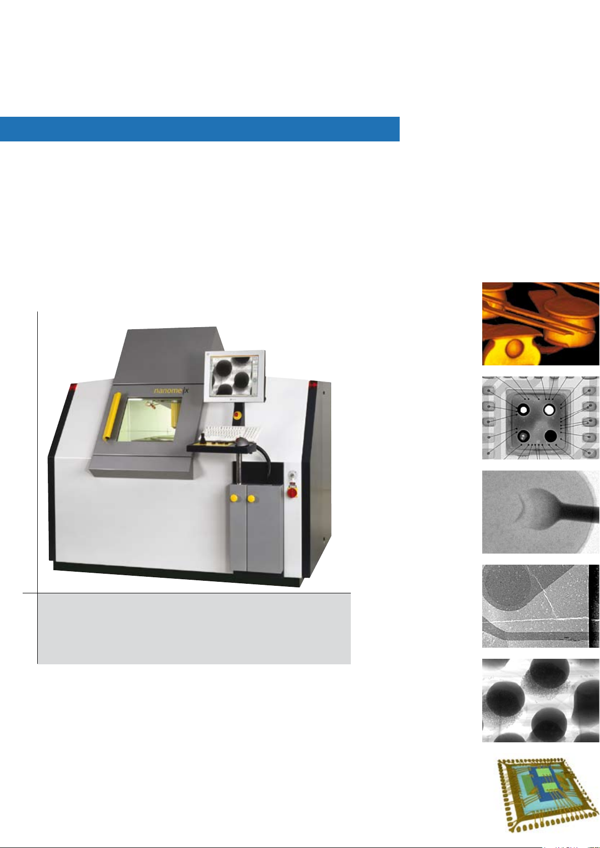
nanome|x – the ultimate X-ray solution
This automatic X-ray system of superior specifications satisfies even highest demands for the
inspection of high-end interconnections in the semiconductor and SMT industry. The high-performance nanofocus tube (4-in-1) covers the full range from submicron resolution to high-intensity applications. The digital realtime image chain provides an excellent contrast resolution and
enables oblique views up to 70 degrees and magnifications well above 24 000x. The nanome|x
offers unique performance and versatility and can be used for 2D X-ray inspection as well as for
full 3D computed tomography. With the new x|act software package the nanome|x is the system
of choice to ensure meeting actual and future zero defect requirements.
Setting new standards
180 kV / 15 W high-power nanofocus tube
2-Megapixel digital image chain
24” TFT monitor
nanoCT® of CSP solder joints
QFN: two open joints
Wedge-bond
Cracked die
x|act software package: easy and fast CAD based programming for high-
resolution automated X-ray inspection (µAXI) with high magnification and
repeatability
Outstanding ease-of-use
Detail detectability down to 0.2 microns
Optical zoom up to 24 000x
Oblique views at angles between 0 and 70 degrees
Dual detector (digital image chain and active temperature-stabilized digital
detector with 30 fps) for brilliant live images
4-Megapixel digital image chain available
Upgradeable to nanoCT
®
BGA: insucient reow
nanoCT® of stacked dies
Page 2

GE
Measurement & Control Solutions
phoenix|x-ray
nanofocus X-ray inspection of high-end interconnections
Electronic packages are sophisticated electronic devices with complex, internal features. In order to meet the quality requirements of the industry, X-ray inspection solutions must not only be
capable of delivering detail detectabilities in the submicron range but also of detecting hidden
defects and flaws. With its nanofocus technology, the nanome|x provides focal spot sizes in the
submicron range to ensure very little geometric fuzziness and greater resolution allowing it to resolve image features as small as 200 nanometers. The two images on the right side clearly show:
the smaller the focal spot, the sharper the image.
microfocus: focal spot 5 microns
nanofocus: focal spot < 1 micron
x|a ct
mee ti ng zero -de fe ct quali ty s tand ard s
As a solution for µAXI with extreme high defect coverage, phoenix|x-ray provides its high precision off-line µAXI system nanome|x including the unique x|act software package for fast and easy
offline CAD programming. Outstanding precision and repeatability, small views with resolutions
of only a few micrometers, 360° rotation and oblique viewing up to 70° ensures meeting highest
quality standards. Besides the automated X-ray inspection, the µAXI system can be used for manual failure analysis or 3D computed tomography as well.
Efficient CAD programming - minimized setup time
3D auto-referencing - optimized positioning accuracy
Live 3D CAD overlay - easy pad identification even in oblique
viewing and rotation
nan oCT
hig h- res olut ion 3 D i magin g
®
Automated multiple die inspection
Live CAD overlay with inspection results
>
For high resolution 3D analysis of smaller samples, the nanome|x system can be upgraded for
full 3D computed tomography. High power nanofocus X-ray technology paired with a fast reconstruction software deliver unrivaled, highest-quality inspection results with nanoCT® image
resolutions.
The 3D nanoCT® image on the right side shows, that each individual die attach is clearly visi-
ble and can be examined for voids.
GE Sensing & Inspection
Technologies GmbH
phoenix|x-ray
Niels-Bohr-Str. 7
D-31515 Wunstorf | Germany
Tel.: + 49 5031.172-0
Fax.: + 49 5031.172-299
phoenix-info@ge.com
3D nanoCT® of stacked dies
Pores in a single die attach
Further offices:
phoenix-stuttgart@ge.com
phoenix-muenchen@ge.com
phoenix-france@ge.com
phoenix-asia@ge.com
phoenix-usa@ge.com
www.gesensinginspection.com
>
GEIT-31202EN (0910)
 Loading...