

Page 1
GE Energy Connections
Grid Solutions
MiCOM P40 Agile
P747
Technical Manual
Busbar Protection IED
Hardware version: A
Publication reference: P747-TM-EN-1.1
Software version: 2
Page 2

Page 3

Contents
P747-TM-EN-1.1
Chapter 1 Introduction 1
1 Chapter Overview 3
2 Foreword 4
2.1 Target Audience 4
2.2 Typographical Conventions 4
2.3 Nomenclature 4
2.4 Product Scope 5
3 Features and Functions 6
3.1 Protection Functions 6
3.2 Control Functions 6
3.3 Measurement Functions 6
3.4 Communication Functions 7
4 Compliance 8
5 Functional Overview 9
6 Ordering Options 10
Chapter 2 Safety Information 11
1 Chapter Overview 13
2 Health and Safety 14
3 Symbols 15
4 Installation, Commissioning and Servicing 16
4.1 Lifting Hazards 16
4.2 Electrical Hazards 16
4.3 UL/CSA/CUL Requirements 17
4.4 Fusing Requirements 17
4.5 Equipment Connections 18
4.6 Protection Class 1 Equipment Requirements 18
4.7 Pre-energization Checklist 19
4.8 Peripheral Circuitry 20
4.9 Upgrading/Servicing 20
5 Decommissioning and Disposal 21
Chapter 3 Hardware Design 23
1 Chapter Overview 25
2 Hardware Architecture 26
3 Mechanical Implementation 27
3.1 Housing Variants 27
3.2 List of Boards 28
4 Front Panel 29
4.1 Front Panel 29
4.1.1 Top compartment with hinged cover 30
4.1.2 Keypad 30
4.1.3 Liquid Crystal Display 30
4.1.4 Front Serial Port (SK1) 30
4.1.5 Front Parallel Port (SK2) 31
4.1.6 Fixed Function LEDs 31
4.1.7 Function Keys 32
4.1.8 Programable LEDs 32
5 Rear Panel 33
6 Boards and Modules 35
6.1 PCBs 35
6.2 Subassemblies 35
Page 4

Contents MiCOM P747
P747-TM-EN-1.1
6.3 Main Processor Board 36
6.4 Combined Coprocessor and Isolated Input Board 37
6.5 Power Supply Board 38
6.5.1 Watchdog 40
6.5.2 Rear Serial Port 41
6.6 Input Module - 2 Transformer Boards 42
6.6.1 Sigma-Delta Input Module Circuit Description 43
6.6.2 Transformer Board 45
6.6.3 Main Input Board 46
6.7 Standard Output Relay Board 47
6.8 IRIG-B Board 49
6.9 Fibre Optic Board 50
6.10 Rear Communication Board 51
6.11 Ethernet Board 52
6.12 Redundant Ethernet Board 53
Chapter 4 Configuration 55
1 Chapter Overview 57
2 Using the HMI Panel 58
2.1 Navigating the HMI Panel 59
2.2 Getting Started 59
2.3 Default Display 60
2.4 Default Display Navigation 61
2.5 Password Entry 61
2.6 Processing Alarms and Fault Records 62
2.7 Menu Structure 63
2.8 Changing the Settings 64
2.9 Direct Access (The Hotkey menu) 64
2.9.1 Setting Group Selection 65
2.9.2 Control Inputs 65
2.9.3 Circuit Breaker Control 66
2.10 Function Keys 66
3 Configuring the Data Protocols 68
3.1 Courier Configuration 68
3.2 DNP3 Configuration 70
3.2.1 DNP3 Configurator 71
3.3 IEC 60870-5-103 Configuration 71
3.4 MODBUS Configuration 73
3.5 IEC 61850 Configuration 74
3.5.1 IEC 61850 Configuration Banks 75
3.5.2 IEC 61850 Network Connectivity 75
4 Date and Time Configuration 76
4.1 Time Zone Compensation 76
4.2 Daylight Saving Time Compensation 76
5 Configuration Settings 78
5.1 System Data 78
5.2 Date and Time 83
5.3 General Configuration 84
5.4 Transformer Ratios 86
5.5 System Configuration 90
5.6 Security Configuration 95
Chapter 5 Protection Functions 97
1 Chapter Overview 99
2 Busbar Protection 100
ii P747-TM-EN-1
Page 5

MiCOM P747 Contents
P747-TM-EN-1.1
2.1 Unit Protection 100
2.2 Current Differential Protection Principles 100
2.3 Through Fault Stability 101
2.4 Bias Current Compensation 101
3 Busbar Multiple Tripping Criteria 103
3.1 Tripping Criteria DDBs 103
3.2 Topology Replica Function 104
3.3 Topology Replica Function DDBs 105
3.4 Zone Current Differential Elements 106
3.5 Check Zone 106
3.5.1 Check Zone Supervision 107
3.5.2 Auxiliary Contacts Discrepancy 107
3.6 Continuous Supervision of Current Circuits (Circuitry Fail) 107
3.7 Current Phase Comparison Check 108
3.8 Optional Voltage Criteria 109
3.9 Instantaneous or Delayed Tripping 109
3.10 Dead Zone (Blind Spot) Protection 109
3.11 Dead Zone (Blind Spot) Protection Logic 110
3.12 Dead Zone (Blind Spot) Protection DDBs 110
4 Circuit Breaker Fail Protection 111
4.1 Circuit Breaker Fail Implementation 111
4.2 Circuit Breaker Fail Logic 111
4.3 CB Fail Settings 113
4.4 CB Fail DDB signals 114
5 Backup Overcurrent Protection 116
5.1 Overcurrent 1 Settings 116
5.2 Overcurrent 2 Settings 121
5.3 Overcurrent DDB signals 133
6 Configuring the Busbar Protection 137
6.1 Example of Configuring the Busbar Protection 137
Chapter 6 Monitoring and Control 141
1 Chapter Overview 143
2 Event Records 144
2.1 Event Records Table 144
2.2 Event Types 151
2.2.1 Opto-input Events 152
2.2.2 Contact Events 152
2.2.3 Alarm Events 152
2.2.4 Fault Record Events 155
2.2.5 Maintenance Events 156
2.2.6 Protection Events 157
2.2.7 Security Events 157
2.2.8 Platform Events 158
2.3 View Records Column 158
3 Disturbance Recorder 161
4 Measurements 162
4.1 Measured Quantities 162
4.1.1 Measured and Calculated Currents 162
4.1.2 Measured and Calculated Voltages 162
4.1.3 Power and Energy Quantities 162
4.1.4 Demand Values 163
4.1.5 Frequency Measurements 163
4.1.6 Other Measurements 163
4.2 Measurement Setup 163
4.3 Measurement Tables 164
P747-TM-EN-1 iii
Page 6

Contents MiCOM P747
P747-TM-EN-1.1
4.4 Measurement Table 3 167
5 I/O Functions 168
5.1 Function Keys 168
5.1.1 Function Key DDB Signals 168
5.1.2 Function Key Settings 169
5.2 LEDs 169
5.2.1 Fixed Function LEDs 169
5.2.2 Programable LEDs 170
5.2.3 Function Key LEDs 170
5.2.4 Trip LED Logic 170
5.2.5 LED DDB Signals 170
5.2.6 LED Conditioners 172
5.3 Opto-inputs 172
5.3.1 Opto-input Configuration 172
5.3.2 Opto-input Labels 175
5.3.3 Opto-input DDB Signals 177
5.3.4 Enhanced Time Stamping 178
5.4 Output Relays 178
5.4.1 Output Relay Labels 178
5.4.2 Output Relay DDB Signals 180
5.4.3 Output Relay Conditioners 180
5.5 Control Inputs 180
5.5.1 Control Input Settings 180
5.5.2 Control Input Configuration 182
5.5.3 Control Input Labels 186
5.5.4 Control Input DDB Signals 186
6 Voltage Transformer Supervision 187
7 Trip Circuit Supervision 188
7.1 Trip Circuit Supervision Scheme 1 188
7.1.1 PSL for TCS Scheme 1 189
7.2 Trip Circuit Supervision Scheme 2 189
7.2.1 PSL for TCS Scheme 2 190
7.3 Trip Circuit Supervision Scheme 3 190
7.3.1 PSL for TCS Scheme 3 190
Chapter 7 SCADA Communications 191
1 Chapter Overview 193
2 Communication Interfaces 194
3 Serial Communication 195
3.1 EIA(RS)232 Bus 195
3.2 EIA(RS)485 Bus 195
3.2.1 EIA(RS)485 Biasing Requirements 196
3.3 K-Bus 196
4 Standard Ethernet Communication 198
5 Overview of Data Protocols 199
6 Courier 200
6.1 Physical Connection and Link Layer 200
6.2 Courier Database 200
6.3 Settings Categories 200
6.4 Setting Changes 200
6.5 Settings Transfer 201
6.6 Event Extraction 201
6.6.1 Automatic Event Record Extraction 201
6.6.2 Manual Event Record Extraction 201
6.7 Disturbance Record Extraction 202
6.8 Programmable Scheme Logic Settings 203
6.9 Time Synchronisation 203
iv P747-TM-EN-1
Page 7

MiCOM P747 Contents
P747-TM-EN-1.1
6.10 Configuration 203
7 IEC 60870-5-103 204
7.1 Physical Connection and Link Layer 204
7.2 Initialisation 204
7.3 Time Synchronisation 205
7.4 Spontaneous Events 205
7.5 General Interrogation (GI) 205
7.6 Cyclic Measurements 205
7.7 Commands 205
7.8 Test Mode 205
7.9 Disturbance Records 205
7.10 Command/Monitor Blocking 206
7.11 Configuration 206
8 DNP 3.0 207
8.1 Physical Connection and Link Layer 207
8.2 Object 1 Binary Inputs 207
8.3 Object 10 Binary Outputs 207
8.4 Object 20 Binary Counters 208
8.5 Object 30 Analogue Input 208
8.6 Object 40 Analogue Output 209
8.7 Object 50 Time Synchronisation 209
8.8 Configuration 209
9 MODBUS 210
9.1 Physical Connection and Link Layer 210
9.2 MODBUS Functions 210
9.3 Response Codes 210
9.4 Register Mapping 211
9.5 Event Extraction 211
9.5.1 Automatic Event Record Extraction 211
9.5.2 Manual Event Record Extraction 212
9.5.3 Record Data 212
9.6 Disturbance Record Extraction 213
9.6.1 Manual Extraction Procedure 214
9.6.2 Automatic Extraction Procedure 215
9.6.3 Extracting the Disturbance Data 217
9.7 Setting Changes 220
9.8 Password Protection 220
9.9 Protection and Disturbance Recorder Settings 220
9.10 Time Synchronisation 221
9.11 Power and Energy Measurement Data Formats 222
10 IEC 61850 223
10.1 Benefits of IEC 61850 223
10.2 IEC 61850 Interoperability 223
10.3 The IEC 61850 Data Model 223
10.4 IEC 61850 in MiCOM IEDs 224
10.5 IEC 61850 Data Model Implementation 225
10.6 IEC 61850 Communication Services Implementation 225
10.7 IEC 61850 Peer-to-peer (GSSE) communications 225
10.8 Mapping GOOSE Messages to Virtual Inputs 226
10.8.1 IEC 61850 GOOSE Configuration 226
10.9 Ethernet Functionality 226
10.9.1 Ethernet Disconnection 226
10.9.2 Loss of Power 226
10.10 IEC 61850 Configurator Settings 226
11 Read Only Mode 229
11.1 IEC 60870-5-103 Protocol 229
11.2 Courier Protocol 229
P747-TM-EN-1 v
Page 8

Contents MiCOM P747
P747-TM-EN-1.1
11.3 IEC 61850 Protocol 230
11.4 Read-Only Settings 230
11.5 Read-Only DDB Signals 230
12 Time Synchronisation 231
13 Demodulated IRIG-B 232
13.1 IRIG-B Implementation 232
14 SNTP 233
15 Time Synchronsiation using the Communication Protocols 234
16 Communication Settings 235
Chapter 8 Redundant Ethernet 239
1 Chapter Overview 241
2 Board Versions 242
3 Board Connections 243
4 Redundancy Protocols 244
4.1 Parallel Redundancy Protocol (PRP) 244
4.1.1 PRP Networks 244
4.1.2 Network Elements 244
4.2 Rapid Spanning Tree Protocol (RSTP) 246
4.3 Self-Healing Protocol (SHP) 247
4.4 Dual-Homing Protocol (DHP) 249
5 Generic Functions for Redundant Ethernet Boards 252
5.1 Forwarding 252
5.1.1 Priority Tagging 252
5.2 Simple Network Management Protocol (SNMP) 252
5.3 SNMP MIB Structure for RSTP, DHP and SHP 253
5.4 SNMP MIB Structure for PRP 254
5.5 Simple Network Time Protocol (SNTP) 257
6 Configuring IP Addresses 258
6.1 Configuring the IED IP Address 258
6.2 Configuring the Board IP Address 258
6.2.1 Configuring the First Two Octets of the Board IP Address 259
6.2.2 Configuring the Third Octet of the Board IP Address 259
6.2.3 Configuring the Last Octet of the Board IP Address 259
7 PRP Configurator 262
7.1 Connecting the IED to a PC 262
7.2 Installing the Configurator 262
7.3 Starting the Configurator 263
7.4 PRP Device Identification 263
7.5 PRP IP Address Configuration 263
7.6 SNTP IP Address Configuration 263
7.7 Check for Connected Equipment 263
7.8 PRP Configuration 264
7.9 Filtering Database 264
7.10 End of Session 264
8 RSTP Configurator 265
8.1 Connecting the IED to a PC 265
8.2 Installing the Configurator 265
8.3 Starting the Configurator 266
8.4 RSTP Device Identification 266
8.5 RSTP IP Address Configuration 266
8.6 SNTP IP Address Configuration 266
8.7 Check for Connected Equipment 267
8.8 RSTP Configuration 267
8.8.1 Bridge parameters 267
8.8.2 Port Parameters 267
vi P747-TM-EN-1
Page 9

MiCOM P747 Contents
P747-TM-EN-1.1
8.8.3 Port States 268
8.9 End of Session 268
9 Switch Manager 269
9.1 Installation 269
9.2 Setup 270
9.3 Network Setup 270
9.4 Bandwidth Used 270
9.5 Reset Counters 270
9.6 Check for Connected Equipment 271
9.7 Mirroring Function 271
9.8 Ports On/Off 271
9.9 VLAN 271
9.10 End of Session 272
Chapter 9 Cyber-Security 273
1 Overview 275
2 The Need for Cyber-Security 276
3 Standards 277
3.1 NERC Compliance 277
3.1.1 CIP 002 278
3.1.2 CIP 003 278
3.1.3 CIP 004 278
3.1.4 CIP 005 278
3.1.5 CIP 006 278
3.1.6 CIP 007 279
3.1.7 CIP 008 279
3.1.8 CIP 009 279
3.2 IEEE 1686-2007 279
4 Cyber-Security Implementation 281
4.1 NERC-Compliant Display 281
4.2 Four-level Access 282
4.2.1 Blank Passwords 283
4.2.2 Password Rules 283
4.2.3 Access Level DDBs 284
4.3 Enhanced Password Security 284
4.3.1 Password Strengthening 284
4.3.2 Password Validation 284
4.3.3 Password Blocking 285
4.4 Password Recovery 286
4.4.1 Password Recovery 286
4.4.2 Password Encryption 287
4.5 Disabling Physical Ports 287
4.6 Disabling Logical Ports 287
4.7 Security Events Management 288
4.8 Logging Out 290
5 Cyber-Security Settings 291
Chapter 10 Settings Application Software 293
1 Introduction to the Settings Application Software 295
1.1 Getting Started 295
1.1.1 Quick System Guide 296
1.1.2 Download Data Models 297
1.1.3 Set Up a System 297
1.1.4 Connect to an IED Front Port 297
1.1.5 Connect to an IED in a System 297
1.1.6 Send Settings to a Device 297
P747-TM-EN-1 vii
Page 10

Contents MiCOM P747
P747-TM-EN-1.1
1.1.7 Extract Settings From a Device 297
1.1.8 Extract a PSL File From a Device 297
1.1.9 Extract a DNP3 File From a Device 298
1.1.10 Extract an Events File From a Device 298
1.1.11 Extract a Disturbance Record From a Device 298
1.2 PSL Editor 298
1.3 IEC 61850 Configurator 298
1.4 DNP3 Configurator 298
1.5 Curve Tool 299
1.6 S&R Courier 299
1.7 AEDR2 299
1.8 WinAEDR2 299
1.9 Wavewin 299
1.10 Device (Menu) Text Editor 300
1.11 Event Viewer 300
1.12 GOOSE Editor 300
1.13 PRP Configurator 300
1.14 RSTP Configurator 300
1.15 Switch Manager 301
Chapter 11 Busbar Commissioning Tool 303
1 P747 Busbar Commissioning Tool (Remote HMI) 305
2 Scheme Editor 306
2.1 Connections 306
2.1.1 Manual Connections 306
2.1.2 Automatic Connections 306
2.1.3 Remove Connection 307
2.2 Scheme Elements 307
2.2.1 Add Elements to a Scheme 307
2.2.2 Remove an Element 307
2.2.3 Group Elements in a Scheme 307
2.2.4 Rotate Elements in a Group 307
2.3 Working with Text on the Scheme 307
2.3.1 Add a Label to an Element 308
2.3.2 Remove a Label From an Element 308
2.3.3 Change an Element's Label 308
2.3.4 Add or Remove Free Text 308
2.3.5 Validate a Scheme 308
3 Protection Data Monitor 309
3.1 Connect to the IED 309
3.1.1 Polling Timer 309
3.1.2 Read IED Data 309
3.1.3 Measurements Data 309
Chapter 12 Scheme Logic 311
1 Chapter Overview 313
2 Introduction to the Scheme Logic 314
3 Fixed Scheme Logic 316
3.1 Any Start Logic 317
3.2 VTS Acceleration Indication Logic 318
3.3 CB Fail SEF Protection Logic 318
3.4 CB Fail Non Current Protection Logic 319
3.5 Composite Earth Fault Start Logic 320
3.6 Any Trip Logic 320
3.7 SEF Any Start Logic 320
4 Programmable Scheme Logic 321
viii P747-TM-EN-1
Page 11

MiCOM P747 Contents
P747-TM-EN-1.1
4.1 Viewing and Printing PSL Diagrams 321
4.2 Trip Output Mappings 322
4.3 Opto-Input Mappings 323
4.4 Output Relay Mappings 324
4.5 LED Mappings 325
4.6 Control Input Mappings 325
4.7 Function Key Mappings 325
4.8 Circuit Breaker Mapping 326
4.9 Fault Record Trigger Mapping 326
4.10 Check Synchronisation and Voltage Monitor Mappings 326
4.11 Settings 326
Chapter 13 Installation 329
1 Chapter Overview 331
2 Handling the Goods 332
2.1 Receipt of the Goods 332
2.2 Unpacking the Goods 332
2.3 Storing the Goods 332
2.4 Dismantling the Goods 332
3 Mounting the Device 333
3.1 Flush Panel Mounting 333
3.2 Rack Mounting 334
4 Cables and Connectors 336
4.1 Terminal Blocks 336
4.2 Power Supply Connections 337
4.3 Earth Connnection 337
4.4 Current Transformers 337
4.5 Voltage Transformer Connections 338
4.6 Watchdog Connections 338
4.7 EIA(RS)485 and K-Bus Connections 338
4.8 IRIG-B Connection 338
4.9 Opto-input Connections 338
4.10 Output Relay Connections 338
4.11 Ethernet Metallic Connections 339
4.12 Ethernet Fibre Connections 339
4.13 RS232 connection 339
4.14 Download/Monitor Port 339
4.15 GPS Fibre Connection 339
4.16 Fibre Communication Connections 339
5 Case Dimensions 340
5.1 Case Dimensions 80TE 340
Chapter 14 Commissioning Instructions 341
1 Chapter Overview 343
2 General Guidelines 344
3 Commissioning Test Menu 345
3.1 Opto I/P Status Cell (Opto-input Status) 345
3.2 Relay O/P Status Cell (Relay Output Status) 345
3.3 Test Mode Cell 345
3.4 Test Pattern Cell 346
3.5 Contact Test Cell 346
3.6 Test LEDs Cell 346
3.7 Red and Green LED Status Cells 346
3.8 PSL Verificiation 346
3.8.1 Test Port Status Cell 346
P747-TM-EN-1 ix
Page 12

Contents MiCOM P747
P747-TM-EN-1.1
3.8.2 Monitor Bit 1 to 8 Cells 346
3.8.3 Using a Monitor Port Test Box 347
4 Commissioning Equipment 348
4.1 Minimum Equipment Required 348
4.2 Optional Equipment Required 348
5 Product Checks 349
5.1 Product Checks with the IED De-energised 349
5.1.1 Visual Inspection 350
5.1.2 Current Transformer Shorting Contacts 350
5.1.3 Insulation 350
5.1.4 External Wiring 351
5.1.5 Watchdog Contacts 351
5.1.6 Power Supply 351
5.2 Product Checks with the IED Energised 351
5.2.1 Watchdog Contacts 352
5.2.2 Test LCD 352
5.2.3 Date and Time 352
5.2.4 Test LEDs 353
5.2.5 Test Alarm and Out-of-Service LEDs 353
5.2.6 Test Trip LED 353
5.2.7 Test User-programmable LEDs 353
5.2.8 Test Opto-inputs 353
5.2.9 Test Output Relays 354
5.2.10 Test Serial Communication Port RP1 354
5.2.11 Test Serial Communication Port RP2 356
5.2.12 Test Ethernet Communication 356
5.2.13 Test Current Inputs 356
5.2.14 Test Voltage Inputs 357
6 Setting Checks 358
6.1 Apply Application-specific Settings 358
6.1.1 Transferring Settings from a Settings File 358
6.1.2 Entering settings using the HMI 358
7 Busbar Protection Checks 360
7.1 Busbar Differential Protection Checks 360
7.2 Connecting the Test Circuit 360
7.3 Performing the Test 360
7.4 Check the Operating Time 361
8 Onload Checks 362
8.1 Confirm Current Connections 362
8.2 Confirm Voltage Connections 362
8.3 On-Load Busbar Differential Test 363
9 Final Checks 364
10 Commissioning Test Settings 365
Chapter 15 Maintenance and Troubleshooting 367
1 Chapter Overview 369
2 Maintenance 370
2.1 Maintenance Checks 370
2.1.1 Alarms 370
2.1.2 Opto-isolators 370
2.1.3 Output Relays 370
2.1.4 Measurement Accuracy 370
2.2 Replacing the Device 371
2.3 Repairing the Device 372
2.4 Removing the front panel 373
2.5 Replacing PCBs 373
2.5.1 Replacing the main processor board 374
x P747-TM-EN-1
Page 13

MiCOM P747 Contents
P747-TM-EN-1.1
2.5.2 Replacement of communications boards 374
2.5.3 Replacement of the input module 375
2.5.4 Replacement of the power supply board 376
2.5.5 Replacement of the I/O boards 376
2.6 Recalibration 376
2.7 Changing the battery 377
2.7.1 Post Modification Tests 377
2.7.2 Battery Disposal 377
2.8 Cleaning 377
3 Troubleshooting 378
3.1 Self-Diagnostic Software 378
3.2 Power-up Errors 378
3.3 Error Message or Code on Power-up 378
3.4 Out of Service LED on at power-up 379
3.5 Error Code during Operation 380
3.5.1 Backup Battery 380
3.6 Mal-operation during testing 380
3.6.1 Failure of Output Contacts 380
3.6.2 Failure of Opto-inputs 380
3.6.3 Incorrect Analogue Signals 381
3.7 PSL Editor Troubleshooting 381
3.7.1 Diagram Reconstruction 381
3.7.2 PSL Version Check 381
4 Repair and Modification Procedure 382
Chapter 16 Technical Specifications 383
1 Chapter Overview 385
2 Interfaces 386
2.1 Front Serial Port 386
2.2 Download/Monitor Port 386
2.3 Rear Serial Port 1 386
2.4 Fibre Rear Serial Port 1 386
2.5 Rear Serial Port 2 387
2.6 Redundant Ethernet Ports 387
2.7 IRIG-B (Demodulated) 387
2.8 IRIG-B (Modulated) 387
2.9 Rear Ethernet Port Copper 388
2.10 Rear Ethernet Port Fibre 388
2.10.1 100 Base FX Receiver Characteristics 388
2.10.2 100 Base FX Transmitter Characteristics 389
3 Busbar Protection Functions 390
3.1 Busbar Circuitry Fault Protection 390
3.2 Busbar Circuitry Fault Protection 390
3.3 Busbar Dead Zone Protection 390
3.4 Three-phase Overcurrent Protection 390
3.5 Earth Fault Protection 391
3.6 Transient Overreach and Overshoot 391
4 Performance of Monitoring and Control Functions 392
4.1 Voltage Transformer Supervision 392
4.2 PSL Timers 392
5 Measurements and Recording 393
5.1 General 393
5.2 Disturbance Records 393
5.3 Event, Fault and Maintenance Records 393
5.4 Fault Locator 393
6 Standards Compliance 394
P747-TM-EN-1 xi
Page 14

Contents MiCOM P747
P747-TM-EN-1.1
6.1 EMC Compliance: 2004/108/EC 394
6.2 Product Safety: 2006/95/EC 394
6.3 R&TTE Compliance 394
6.4 UL/CUL Compliance 394
7 Mechanical Specifications 395
7.1 Physical Parameters 395
7.2 Enclosure Protection 395
7.3 Mechanical Robustness 395
7.4 Transit Packaging Performance 395
8 Ratings 396
8.1 AC Measuring Inputs 396
8.2 Current Transformer Inputs 396
8.3 Voltage Transformer Inputs 396
8.4 Auxiliary Supply Voltage 396
8.5 Nominal Burden 397
8.6 Power Supply Interruption 397
8.7 Standard Output Contacts 398
8.8 Watchdog Contacts 398
8.9 Isolated Digital Inputs 399
8.9.1 Nominal Pickup and Reset Thresholds 399
9 Environmental Conditions 400
9.1 Ambient Temperature Range 400
9.2 Ambient Humidity Range 400
9.3 Corrosive Environments 400
10 Type Tests 401
10.1 Insulation 401
10.2 Creepage Distances and Clearances 401
10.3 High Voltage (Dielectric) Withstand 401
10.4 Impulse Voltage Withstand Test 401
11 Electromagnetic Compatibility 402
11.1 1 MHz Burst High Frequency Disturbance Test 402
11.2 Damped Oscillatory Test 402
11.3 Immunity to Electrostatic Discharge 402
11.4 Electrical Fast Transient or Burst Requirements 402
11.5 Surge Withstand Capability 402
11.6 Surge Immunity Test 403
11.7 Immunity to Radiated Electromagnetic Energy 403
11.8 Radiated Immunity from Digital Communications 403
11.9 Radiated Immunity from Digital Radio Telephones 403
11.10 Immunity to Conducted Disturbances Induced by Radio Frequency Fields 403
11.11 Magnetic Field Immunity 404
11.12 Conducted Emissions 404
11.13 Radiated Emissions 404
11.14 Power Frequency 404
Appendix A Symbols and Glossary 405
1 Chapter Overview 407
2 Acronyms and Abbreviations 408
3 Units for Digital Communications 414
4 American Vs British English Terminology 415
5 Logic Symbols and Terms 416
6 Logic Timers 420
7 Logic Gates 422
Appendix B Commissioning Record 423
xii P747-TM-EN-1
Page 15

MiCOM P747 Contents
P747-TM-EN-1.1
1 Test Record 425
1.1 Engineer Details 425
1.2 Front Plate Information 425
1.3 Test Equipment 425
1.4 Tests with Product De-energised 425
1.5 Tests with Product Energised 426
1.6 Communication Tests 426
1.7 Current Input Tests 426
1.8 Voltage Input Tests 427
1.9 Overcurrent Checks 427
1.10 On-load Checks 427
1.11 Final Checks 427
Appendix C Wiring Diagrams 429
1 Appendix Overview 431
2 P747: Busbar Protection 432
3 P747: I/O Option A 433
4 P747: I/O Option B 434
5 P747: I/O Option C 435
P747-TM-EN-1 xiii
Page 16

Contents MiCOM P747
P747-TM-EN-1.1
xiv P747-TM-EN-1
Page 17

Table of Figures
P747-TM-EN-1.1
Figure 1: Functional Overview 9
Figure 2: Hardware architecture 26
Figure 3: Exploded view of IED 27
Figure 4: Front panel (80TE) 29
Figure 5: Rear view of populated 80TE case 33
Figure 6: Terminal block types 34
Figure 7: Rear connection to terminal block 35
Figure 8: Main processor board 36
Figure 9: Combined coprocessor and isolated digital input board 37
Figure 10: Power supply board 38
Figure 11: Power Supply Assembly 39
Figure 12: Power Supply Terminals 40
Figure 13: Watchdog contact terminals 41
Figure 14: Rear serial port terminals 42
Figure 15: Input Module - 1 transformer board 42
Figure 16: Input module schematic 43
Figure 17: Instrument Transformer board 45
Figure 18: Main input board 46
Figure 19: Output relay board - 8 contacts 47
Figure 20: IRIG-B board 49
Figure 21: Fibre optic board 50
Figure 22: Rear communication board 51
Figure 23: Ethernet board 52
Figure 24: Redundant Ethernet board 53
Figure 25: Menu navigation 59
Figure 26: Default display navigation 61
Figure 27: Current Differential Protection 100
Figure 28: Compensation using biased differential characteristic 102
Figure 29: Multiple tripping criteria 103
Figure 30: Topology replica function 104
Figure 31: Zone tripping characteristic. 106
Figure 32: Check zone supervision characteristic. 107
Figure 33: Circuitry check characteristic. 108
Figure 34: Example of busbar dead-zone 110
Figure 35: Dead-zone logic 110
Figure 36: CBF initiated by internal signal 112
Figure 37: CBF initiated by external signal 113
Figure 38: Busbar topology used in configuration example. 137
Page 18

Table of Figures MiCOM P747
P747-TM-EN-1.1
Figure 39: Fault recorder stop conditions 155
Figure 40: Trip LED logic 170
Figure 41: TCS Scheme 1 188
Figure 42: PSL for TCS Scheme 1 189
Figure 43: TCS Scheme 2 189
Figure 44: PSL for TCS Scheme 2 190
Figure 45: TCS Scheme 3 190
Figure 46: PSL for TCS Scheme 3 190
Figure 47: RS485 biasing circuit 196
Figure 48: Remote communication using K-Bus 197
Figure 49: Control input behaviour 208
Figure 50: Manual selection of a disturbance record 215
Figure 51: Automatic selection of disturbance record - method 1 216
Figure 52: Automatic selection of disturbance record - method 2 217
Figure 53: Configuration file extraction 218
Figure 54: Data file extraction 219
Figure 55: Data model layers in IEC61850 224
Figure 56: GPS Satellite timing signal 232
Figure 57: Board connectors 243
Figure 58: Example PRP redundant network 245
Figure 59: Application of PRP at substation level 246
Figure 60: IED attached to redundant Ethernet star or ring circuit 247
Figure 61: IED, bay computer and Ethernet switch with self healing ring facilities 247
Figure 62: Internal architecture of IED, C264 bay computer and H36x Ethernet switch 248
Figure 63: Redundant Ethernet ring architecture with IED, bay computer and Ethernet
249
switches
Figure 64: Redundant Ethernet ring architecture with IED, bay computer and Ethernet
249
switches after failure
Figure 65: Dual homing mechanism 250
Figure 66: Application of Dual Homing Star at substation level 251
Figure 67: SNMP MIB tree 253
Figure 68: IED and REB IP address configuration 258
Figure 69: Connection using (a) an Ethernet switch and (b) a media converter 262
Figure 70: Connection using (a) an Ethernet switch and (b) a media converter 265
Figure 71: Default display navigation 282
Figure 72: Flowchart showing how S1 Agile can be used to set up and save a protection
Figure 73: Scheme Logic Interfaces 314
Figure 74: Any Start Logic 317
Figure 75: VTS Acceleration Indication Logic 318
Figure 76: CB Fail SEF Protection Logic 318
xvi P747-TM-EN-1
296
system offline or online.
Page 19

MiCOM P747 Table of Figures
P747-TM-EN-1.1
Figure 77: CB Fail Non Current Protection Logic 320
Figure 78: Composite Earth Fault Start Logic 320
Figure 79: Any Trip Logic 320
Figure 80: SEF Any Start Logic 320
Figure 81: Trip Output Mappings 322
Figure 82: Opto-Input Mappings 323
Figure 83: Output Relay Mappings 324
Figure 84: LED Mappings 325
Figure 85: Control Input Mappings 325
Figure 86: Function Key Mappings 325
Figure 87: Circuit Breaker mapping 326
Figure 88: Fault Record Trigger mapping 326
Figure 89: Check Synchronisation and Voltage Monitor mappings 326
Figure 90: Location of battery isolation strip 333
Figure 91: Rack mounting of products 335
Figure 92: Terminal block types 336
Figure 93: 80TE case dimensions 340
Figure 94: RP1 physical connection 355
Figure 95: Remote communication using K-bus 355
Figure 96: Possible terminal block types 372
Figure 97: Front panel assembly 374
Figure 98: Logic Gates 422
Figure 99: P747 busbar protection, 3 box solution 432
Figure 100: P747 busbar protection with 40 inputs, 24 outputs and coprocessor 433
Figure 101: P747 busbar protection with 32 inputs, 32 outputs and coprocessor 434
Figure 102: P747 busbar protection with 32 inputs, 24 outputs and standard coprocessor 435
P747-TM-EN-1 xvii
Page 20

Table of Figures MiCOM P747
P747-TM-EN-1.1
xviii P747-TM-EN-1
Page 21

INTRODUCTION
CHAPTER 1
Page 22

Chapter 1 - Introduction MiCOM P747
P747-TM-EN-1.1
2 P747-TM-EN-1
Page 23

MiCOM P747 Chapter 1 - Introduction
P747-TM-EN-1.1
1 CHAPTER OVERVIEW
This chapter contains the following sections:
Chapter Overview 3
Foreword 4
Features and Functions 6
Compliance 8
Functional Overview 9
Ordering Options 10
P747-TM-EN-1 3
Page 24

Chapter 1 - Introduction MiCOM P747
P747-TM-EN-1.1
2 FOREWORD
This technical manual provides a functional and technical description of Alstom Grid's MiCOM P747, as well
as a comprehensive set of instructions for using the device.
We have attempted to make this manual as accurate, comprehensive and user-friendly as possible.
However we cannot guarantee that it is free from errors. Nor can we state that it cannot be improved. We
would therefore be very pleased to hear from you if you discover any errors, or have any suggestions for
improvement. All feedback should be sent to our contact centre via the following URL:
http://www.alstom.com/grid/contactcentre/
2.1 TARGET AUDIENCE
This manual is aimed towards all professionals charged with installing, commissioning, maintaining,
troubleshooting, or operating any of the products within the specified product range. This includes installation
and commissioning personnel as well as engineers who will be responsible for operating the product.
The level at which this manual is written assumes that installation and commissioning engineers have
knowledge of handling electronic equipment. Also, system and protection engineers have a thorough
knowledge of protection systems and associated equipment.
2.2 TYPOGRAPHICAL CONVENTIONS
The following typographical conventions are used throughout this manual.
● The names for special keys and function keys appear in capital letters.
For example: ENTER
● When describing software applications, menu items, buttons, labels etc as they appear on the screen
are written in bold type.
For example: Select Save from the file menu.
● Filenames and paths use the courier font
For example: Example\File.text
● Special terminology is written with leading capitals
For example: Sensitive Earth Fault
● If reference is made to the IED's internal settings and signals database, the menu group heading
(column) text is written in upper case italics
For example: The SYSTEM DATA
● If reference is made to the IED's internal settings and signals database, the setting cells and DDB
signals are written in bold italics
For example: The Language cell in the SYSTEM DATA column
● If reference is made to the IED's internal settings and signals database, the value of a cell's content is
written in the Courier font
For example: The Language cell in the SYSTEM DATA column contains the value English
column
2.3 NOMENCLATURE
Due to the technical nature of this manual, many special terms, abbreviations and acronyms are used
throughout the manual. Some of these terms are well-known industry-specific terms while others may be
special product-specific terms used by Alstom Grid. A glossary at the back of this manual provides a
complete description of all special terms used throughout the manual.
4 P747-TM-EN-1
Page 25

MiCOM P747 Chapter 1 - Introduction
P747-TM-EN-1.1
We would like to highlight the following changes of nomenclature however:
● The word 'relay' is no longer used for the device itself. Instead, the device is referred to as an 'IED'
(Intelligent Electronic Device), the 'device', the 'product', or the 'unit'. The word 'relay' is used purely to
describe the electromechanical components within the device, i.e. the output relays.
● British English is used throughout this manual.
● The British term 'Earth' is used in favour of the American term 'Ground'.
2.4 PRODUCT SCOPE
This product protects busbars with up to 4 zones plus a check zone. It can be applied at any voltage level.
One device is used to protect each phase (3-box solution). A further device can be used to protect the
neutral line (4-box solution). The device is suitable for applications on solidly grounded systems, or where a
centralised scheme is needed.
Each device can manage a maximum of:
● 4 Voltage transformers (VTs) (1 VT per zone),
● 18 Current transformers (CTs)
● 18 Circuit breakers (CBs)
● 72 isolators
● Up to 40 Digital Inputs and 128 Virtual Inputs (128 digital inputs via communications) for each
protected phase
● Up to 32 Digital Outputs and 128 Virtual Outputs (128 digital outputs via communications) for each
protected phase
The P747 consists of the following main components.
Main protection
This uses low impedance biased current differential protection. The typical operating time is less than one
cycle. If a fault occurs and more than one zone needs to be tripped, you might need to trip zones
sequentially. You can do this by setting different time delays on each of the zone differential elements.
Backup protection
This consists of:
● phase overcurrent
● dead zone
● circuit breaker failure
Settings application software
This allows you to create a scheme and display the measured data. The scheme editor allows you to quickly
draw schemes from a library of elements, then validate the scheme. It can also display the status of DDBs
and measured data on the scheme in real time.
Inputs and outputs
The device has many hard-wired digital inputs and outputs. For applications that demand more, virtual inputs
and outputs can be used between the products protecting the different phases. 128 virtual inputs and outputs
can be shared between products using communications links. Use hard-wired inputs and outputs to connect
the most time-critical signals between devices. Use Virtual inputs and outputs to communicate less timecritical information signals between devices.
P747-TM-EN-1 5
Page 26
Chapter 1 - Introduction MiCOM P747
P747-TM-EN-1.1
3 FEATURES AND FUNCTIONS
3.1 PROTECTION FUNCTIONS
The P747 provides the following protection functions:
Protection Function IEC 61850 ANSI
Phase segregated biased current differential high speed busbar protection PhsPDIF 87BB/P
Check Zone segregated biased phase current differential high speed busbar protection CzPPDIF 87CZ/P
Definite Time overcurrent protection (2 stages) OcpPTOC 50/P
IDMT overcurrent protection (2 stages) OcpPTOC 51/P
Dead zone phase protection (short zone between CTs and open CBs) DzpPhsPTOC 50DZ
CB Failure (auxiliary contacts or fast undercurrent) RBRF 50BF
CB Failure and isolator state monitoring
Lockout RBRF 89
Undervoltage control 27
VT blocking scheme based on V< VTS
3.2 CONTROL FUNCTIONS
Feature IEC 61850 ANSI
Watchdog contacts
Read-only mode
NERC compliant cyber-security
Function keys (up to 10) FnkGGIO
Programmable LEDs (up to 18) LedGGIO
Programmable hotkeys (2)
Programmable allocation of digital inputs and outputs
Fully customizable menu texts
Circuit breaker control, status & condition monitoring XCBR 52
Trip circuit and coil supervision
Control inputs PloGGIO1
Power-up diagnostics and continuous self-monitoring
Dual rated 1A and 5A CT inputs
Alternative setting groups (4)
Graphical programmable scheme logic (PSL)
Fault locator RFLO
3.3 MEASUREMENT FUNCTIONS
Measurement of all instantaneous & integrated values
(Exact range of measurements depend on the device model)
Disturbance recorder for waveform capture – specified in samples per
cycle
Fault Records
6 P747-TM-EN-1
Measurement Function IEC 61850 ANSI
MET
RDRE DFR
Page 27
MiCOM P747 Chapter 1 - Introduction
P747-TM-EN-1.1
Measurement Function IEC 61850 ANSI
Maintenance Records
Event Records / Event logging Event records
Time Stamping of Opto-inputs Yes Yes
3.4 COMMUNICATION FUNCTIONS
The device offers the following communication functions:
Feature ANSI
NERC compliant cyber-security
Front RS232 serial communication port for configuration 16S
Rear serial RS485 communication port for SCADA control 16S
2 Additional rear serial communication ports for SCADA control and
teleprotection (fibre and copper) (optional)
Ethernet communication (optional) 16E
Redundant Ethernet communication (optional) 16E
Courier 16S
IEC 61850 (optional) 16E
IEC 60870-5-103 (optional) 16S
DNP3.0 over serial link (optional) 16S
DNP3.0 over Ethernet (optional) 16E
IRIG-B time synchronisation (optional) CLK
16S
P747-TM-EN-1 7
Page 28

Chapter 1 - Introduction MiCOM P747
P747-TM-EN-1.1
4 COMPLIANCE
The device has undergone a range of extensive testing and certification processes to ensure and prove
compatibility with all target markets. Below is a list of standards with which the device is compliant. A detailed
description of these criteria can be found in the Technical Specifications chapter.
Compliance Standards
Condition Compliance
EMC compliance (compulsory) 2004/108/EC (demonstrated by EN60255-26:2009)
Product safety (compulsory) 2006/95/EC (demonstrated by EN60255-27:2005)
R&TTE Compliance (compulsory) 99/5/EC
EMC EN50263, IEC 60255-22-1/2/3/4/5/6/7, IEC 61000-4-5/6/8/9/10/16
EN61000-4-3/18, IEEE/ANSI C37.90.1/2/3, ENV50204, EN55022
Product Safety for North America UL/CL File No. UL/CUL E202519
Environmental conditions IEC 60255-27:2005, IEC 60068-2-78:2001, -30:2005, -42:2003,
-42:2003
Power supply interruption IEC 60255-11, IEC 61000-4-11
Type tests for Insulation, creepage distance and clearances, high
voltage dielectric withstand, and impulse voltage withstand
Enclosure protection IEC 60529:2002 – IP10, IP30, IP52
Mechanical robustness IEC 60255-21-1/2/3
Documentation IEC 60255-151
IEC 60255-27:2005
8 P747-TM-EN-1
Page 29
87BB/P
87CZ/P
50/51
/P
50DZ
50BF
ISL
Remote
Comms. Port
Local
Communication
Fault
Records
Measurements
Disturbance
Records
Binary
Input / Output
LEDs
PSL
E00029
2
7
MiCOM P747 Chapter 1 - Introduction
P747-TM-EN-1.1
5 FUNCTIONAL OVERVIEW
Figure 1: Functional Overview
P747-TM-EN-1 9
Page 30
Variants
P747
Numerical Busbar Differe ntial Protection Relay with 4-zone enha ncements
P747 **
Vx Aux Rating:
New PSU 24-54 Vdc 7
New PSU 48-125 Vdc (40-100 Vac) 8
New PSU 110-250 Vdc (100-240 Vac) 9
In/Vn Rating:
CT1 - CT18 In = 1A/5A, Vn = (100/120V) (18CT/3VT) 1
Hardware Options:
Standard: no options 1
IRIG-B (Modulated) only 2
Fibre optic converter only 3
IRIG-B (Modulated) & fibre optic converter 4
Ethernet with 100 Mbps fibre optic port 6
2nd rear comms port 7
2nd rear comms port + IRIG-B (Modulated) 8
Ethernet (100 Mbps) + IRIG-B (Modulated) A
Ethernet (100 Mps) + IRIG-B (Unmodulated) B
IRIG-B (Unmodulated) C
Redundant Ethernet Self-Healing Ring, 2 multi-mode fibre ports + Modulated IRIG-B G
Redundant Ethernet Self-Healing Ring, 2 multi-mode fibre ports + Un-modulated IRIG-B H
Redundant Ethernet RSTP, 2 multi-mode fibre ports + Modulated IRIG-B J
Redundant Ethernet RSTP, 2 multi-mode fibre ports + Un-modulated IRIG-B K
Redundant Ethernet Dual-Homing Star, 2 multi-mode fibre ports + Modulated IRIG-B L
Redundant Ethernet Dual-Homing Star, 2 multi-mode fibre ports + Un-modulated IRIG-B M
Redundant Ethernet PRP, 2 multi-mode fibre ports + Modulated IRIG-B N
Redundant Ethernet PRP, 2 multi-mode fibre ports + Un-modulated IRIG-B P
Product Specific Options:
Size 16 case, 40 optos + 24 relays + coprocessor A
Size 16 case, 32 optos + 32 relays + coprocessor B
Size 16 case, 32 optos + 24 relays + standard coprocessor C
Protocol Options:
K-Bus/Courier 1
Modbus 2
IEC60870-5-103 3
DNP3.0 4
IEC 61850 over Ethernet and Courier via rear K-Bus/RS485 6
DNP3 over Ethernet with Courier rear port K-Bus/RS485 protocol 8
Mounting Options:
Panel mounting M
Rack mounting N
Langua ge Options:
English, French, German, Spanish 0
English, French, German, Russian 5
Chinese, English or French via HMI, with English or French only via communications port C
Software Version Options:
Unless specified the latest version will be delivered **
Settings File s Options:
Default 0
Customer specific A
Design Suffix:
Extended CPU K
Order Number
E00036
Chapter 1 - Introduction MiCOM P747
P747-TM-EN-1.1
6 ORDERING OPTIONS
10 P747-TM-EN-1
Page 31

SAFETY INFORMATION
CHAPTER 2
Page 32

Chapter 2 - Safety Information MiCOM P747
P747-TM-EN-1.1
12 P747-TM-EN-1
Page 33

MiCOM P747 Chapter 2 - Safety Information
P747-TM-EN-1.1
1 CHAPTER OVERVIEW
This chapter provides information about the safe handling of the equipment. The equipment must be properly
installed and handled in order to maintain it in a safe condition and to keep personnel safe at all times. You
must be familiar with information contained in this chapter before unpacking, installing, commissioning, or
servicing the equipment.
This chapter contains the following sections:
Chapter Overview 13
Health and Safety 14
Symbols 15
Installation, Commissioning and Servicing
Decommissioning and Disposal 21
16
P747-TM-EN-1 13
Page 34

Chapter 2 - Safety Information MiCOM P747
P747-TM-EN-1.1
2 HEALTH AND SAFETY
Personnel associated with the equipment must be familiar with the contents of this Safety Information.
When electrical equipment is in operation, dangerous voltages are present in certain parts of the equipment.
Improper use of the equipment and failure to observe warning notices will endanger personnel.
Only qualified personnel may work on or operate the equipment. Qualified personnel are individuals who:
● Are familiar with the installation, commissioning, and operation of the equipment and the system to
which it is being connected.
● Are familiar with accepted safety engineering practises and are authorised to energise and de-
energise equipment in the correct manner.
● Are trained in the care and use of safety apparatus in accordance with safety engineering practises
● Are trained in emergency procedures (first aid).
Although the documentation provides instructions for installing, commissioning and operating the equipment,
it cannot cover all conceivable circumstances. In the event of questions or problems, do not take any action
without proper authorisation. Please contact the appropriate technical sales office and request the necessary
information.
14 P747-TM-EN-1
Page 35

MiCOM P747 Chapter 2 - Safety Information
P747-TM-EN-1.1
3 SYMBOLS
Throughout this manual you will come across the following symbols. You will also see these symbols on
parts of the equipment.
Caution:
Refer to equipment documentation. Failure to do so could result in damage to
the equipment
Warning:
Risk of electric shock
Earth terminal
Protective Earth terminal
P747-TM-EN-1 15
Page 36

Chapter 2 - Safety Information MiCOM P747
P747-TM-EN-1.1
4 INSTALLATION, COMMISSIONING AND SERVICING
4.1 LIFTING HAZARDS
Plan carefully, identify any possible hazards and determine whether the load needs to be moved at all. Look
at other ways of moving the load to avoid manual handling. Use the correct lifting techniques and Personal
Protective Equipment to reduce the risk of injury.
Many injuries are caused by:
● Lifting heavy objects
● Lifting things incorrectly
● Pushing or pulling heavy objects
● Using the same muscles repetitively
4.2 ELECTRICAL HAZARDS
Caution:
All personnel involved in installing, commissioning, or servicing this equipment
must be familiar with the correct working procedures.
Caution:
Consult the equipment documentation before installing, commissioning, or
servicing the equipment.
Caution:
Always use the equipment in a manner specified by the manufacturer. Failure to
do so will jeopardise the protection provided by the equipment.
Warning:
Removal of equipment panels or covers may expose hazardous live parts. Do
not touch until the electrical power is removed. Take extra care when there is
unlocked access to the rear of the equipment.
Warning:
Isolate the equipment before working on the terminal strips.
Warning:
Use a suitable protective barrier for areas with restricted space, where there is a
risk of electric shock due to exposed terminals.
16 P747-TM-EN-1
Caution:
Disconnect power before disassembling. Disassembly of the equipment may
expose sensitive electronic circuitry. Take suitable precautions against
electrostatic voltage discharge (ESD) to avoid damage to the equipment.
Page 37

MiCOM P747 Chapter 2 - Safety Information
P747-TM-EN-1.1
Caution:
NEVER look into optical fibres. Always use optical power meters to determine
operation or signal level.
Caution:
Insulation testing may leave capacitors charged up to a hazardous voltage. At
the end of each part of the test, discharge the capacitors by reducing the voltage
to zero, before disconnecting the test leads.
Caution:
Operate the equipment within the specified electrical and environmental limits.
Caution:
Before cleaning the equipment, ensure that no connections are energised. Use a
lint free cloth dampened with clean water.
Note:
Contact fingers of test plugs are normally protected by petroleum jelly, which should not be removed.
4.3 UL/CSA/CUL REQUIREMENTS
The information in this section is applicable only to equipment carrying UL/CSA/CUL markings.
Caution:
Equipment intended for rack or panel mounting is for use on a flat surface of a
Type 1 enclosure, as defined by Underwriters Laboratories (UL).
Caution:
To maintain compliance with UL and CSA/CUL, install the equipment using UL/
CSA-recognised parts for: cables, protective fuses, fuse holders and circuit
breakers, insulation crimp terminals, and replacement internal batteries.
4.4 FUSING REQUIREMENTS
Caution:
Where UL/CSA listing of the equipment is required for external fuse protection, a
UL or CSA Listed fuse must be used. The listed protective fuse type is: Class J
time delay fuse, with a maximum current rating of 15 A and a minimum DC rating
of 250 V dc (for example type AJT15).
P747-TM-EN-1 17
Caution:
Where UL/CSA listing of the equipment is not required, a high rupture capacity
(HRC) fuse type with a maximum current rating of 16 Amps and a minimum dc
rating of 250 V dc may be used (for example Red Spot type NIT or TIA).
For P60 models, use a 4A maximum T-type fuse.
Page 38

Chapter 2 - Safety Information MiCOM P747
P747-TM-EN-1.1
Caution:
Auxiliary supply wiring and digital input circuits should be protected by a high
rupture capacity NIT or TIA fuse with maximum rating of 16 A. for safety
reasons, current transformer circuits must never be fused. Other circuits should
be appropriately fused to protect the wire used.
4.5 EQUIPMENT CONNECTIONS
Warning:
Terminals exposed during installation, commissioning and maintenance may
present a hazardous voltage unless the equipment is electrically isolated.
Caution:
Tighten M4 clamping screws of heavy duty terminal block connectors to a
nominal torque of 1.3 Nm.
Tighten captive screws of terminal blocks to 0.5 Nm minimum and 0.6 Nm
maximum.
Caution:
Always use insulated crimp terminations for voltage and current connections.
Caution:
Always use the correct crimp terminal and tool according to the wire size.
Caution:
Watchdog (self-monitoring) contacts are provided to indicate the health of the
device on some products. We strongly recommend that you hard wire these
contacts into the substation's automation system, for alarm purposes.
4.6 PROTECTION CLASS 1 EQUIPMENT REQUIREMENTS
Caution:
Earth the equipment with the supplied PCT (Protective Conductor Terminal).
Caution:
Do not remove the PCT.
18 P747-TM-EN-1
Caution:
The PCT is sometimes used to terminate cable screens. Always check the PCT’s
integrity after adding or removing such earth connections.
Page 39

MiCOM P747 Chapter 2 - Safety Information
P747-TM-EN-1.1
Caution:
Use a locknut or similar mechanism to ensure the integrity of stud-connected
PCTs.
Caution:
The recommended minimum PCT wire size is 2.5
mains supply is 230 V (e.g. Europe) and 3.3 mm² for countries whose mains
supply is 110 V (e.g. North America). This may be superseded by local or
country wiring regulations.
For P60 products, the recommended minimum PCT wire size is 6 mm². See
manual for details.
Caution:
The PCT connection must have low-inductance and be as short as possible.
Caution:
All connections to the equipment must have a defined potential. Connections
that are pre-wired, but not used, should be earthed when binary inputs and
output relays are isolated. When binary inputs and output relays are connected
to a common potential, unused pre-wired connections should be connected to
the common potential of the grouped connections.
mm² for countries whose
4.7 PRE-ENERGIZATION CHECKLIST
Caution:
Check voltage rating/polarity (rating label/equipment documentation).
Caution:
Check CT circuit rating (rating label) and integrity of connections.
Caution:
Check protective fuse or miniature circuit breaker (MCB) rating.
Caution:
Check integrity of the PCT connection.
Caution:
Check voltage and current rating of external wiring, ensuring it is appropriate for
the application.
P747-TM-EN-1 19
Page 40

Chapter 2 - Safety Information MiCOM P747
P747-TM-EN-1.1
4.8 PERIPHERAL CIRCUITRY
Warning:
Do not open the secondary circuit of a live CT since the high voltage produced
may be lethal to personnel and could damage insulation. Short the secondary of
the line CT before opening any connections to it.
Note:
For most Alstom equipment with ring-terminal connections, the threaded terminal block for current transformer
termination is automatically shorted when the module is removed. Therefore external shorting of the CTs may not be
required. Check the equipment documentation first to see if this applies.
Caution:
Where external components such as resistors or voltage dependent resistors
(VDRs) are used, these may present a risk of electric shock or burns if touched.
Warning:
Take extreme care when using external test blocks and test plugs such as the
MMLG, MMLB and MiCOM ALSTOM P990, as hazardous voltages may be
exposed. Ensure that CT shorting links are in place before removing MMLB test
plugs, to avoid potentially lethal voltages.
4.9 UPGRADING/SERVICING
Warning:
Do not insert or withdraw modules, PCBs or expansion boards from the
equipment while energised, as this may result in damage to the equipment.
Hazardous live voltages would also be exposed, endangering personnel.
Caution:
Internal modules and assemblies can be heavy. Take care when inserting or
removing modules into or out of the IED.
20 P747-TM-EN-1
Page 41

MiCOM P747 Chapter 2 - Safety Information
P747-TM-EN-1.1
5 DECOMMISSIONING AND DISPOSAL
Caution:
Before decommissioning, completely isolate the equipment power supplies
(both poles of any dc supply). The auxiliary supply input may have capacitors in
parallel, which may still be charged. To avoid electric shock, discharge the
capacitors using the external terminals before to decommissioning.
Caution:
Avoid incineration or disposal to water courses. Dispose of the equipment in a
safe, responsible an environmentally friendly manner, and if applicable, in
accordance with country-specific regulations.
P747-TM-EN-1 21
Page 42

Chapter 2 - Safety Information MiCOM P747
P747-TM-EN-1.1
22 P747-TM-EN-1
Page 43

HARDWARE DESIGN
CHAPTER 3
Page 44

Chapter 3 - Hardware Design MiCOM P747
P747-TM-EN-1.1
24 P747-TM-EN-1
Page 45

MiCOM P747 Chapter 3 - Hardware Design
P747-TM-EN-1.1
1 CHAPTER OVERVIEW
This chapter provides information about the product's hardware design.
This chapter contains the following sections:
Chapter Overview 25
Hardware Architecture 26
Mechanical Implementation 27
Front Panel 29
Rear Panel 33
Boards and Modules 35
P747-TM-EN-1 25
Page 46

Communications
Analogue Inputs
I/O
I
n
t
e
r
c
o
n
n
e
c
t
i
o
n
Output relay boards
Opto-input boards
CTs
VTs
RS485 modules
Ethernet modules
Keypad
L
CD
LEDs
Front port
Watchdog module
PSU module
Watchdog
c
ontacts
+ LED
Auxiliary
Supply
IRIG-B module
P
r
o
c
e
s
s
o
r
m
o
d
u
l
e
F
r
o
n
t
p
a
n
e
l
H
M
I
Output relay contacts
Digital inputs
P
ower system currents
Power system voltages
RS485 communication
Time synchronisation
Ethernet communication
V00233
Note: Not all modules are applicable to all products
Memory
Flash memory for settings
Battery-backed SRAM
for records
Chapter 3 - Hardware Design MiCOM P747
P747-TM-EN-1.1
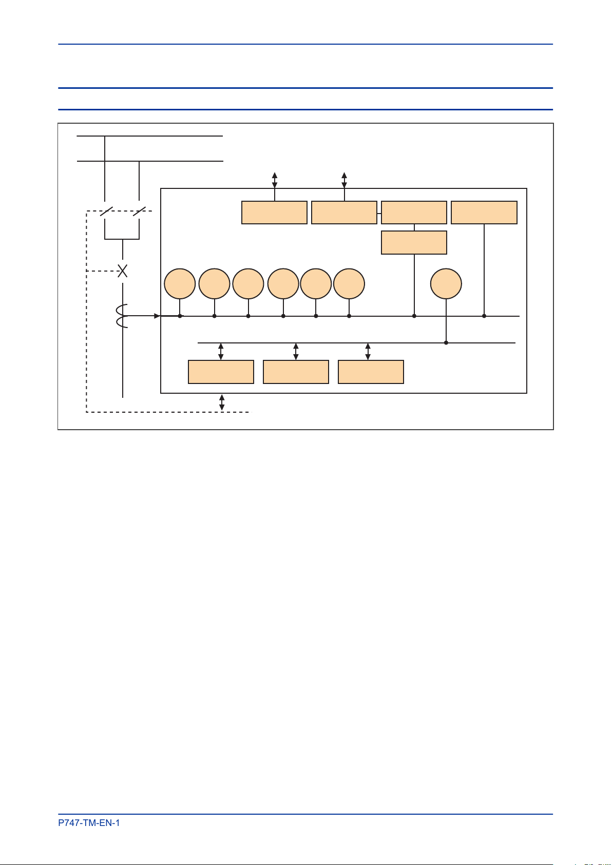
2 HARDWARE ARCHITECTURE
The main components comprising devices based on the Px4x platform are as follows:
● The housing, consisting of a front panel and connections at the rear
● The Main processor module consisting of the main CPU (Central Processing Unit), memory and an
interface to the front panel HMI (Human Machine Interface)
● A selection of plug-in boards and modules with presentation at the rear for the power supply,
communication functions, digital I/O, analogue inputs, and time synchronisation connectivity
All boards and modules are connected by a parallel data and address bus, which allows the processor
module to send and receive information to and from the other modules as required. There is also a separate
serial data bus for conveying sampled data from the input module to the CPU. These parallel and serial
databuses are shown as a single interconnection module in the following figure, which shows typical
modules and the flow of data between them.
Figure 2: Hardware architecture
26 P747-TM-EN-1
Page 47

MiCOM P747 Chapter 3 - Hardware Design
P747-TM-EN-1.1
3 MECHANICAL IMPLEMENTATION
All products based on the Px4x platform have common hardware architecture. The hardware is modular and
consists of the following main parts:
● Case and terminal blocks
● Boards and modules
● Front panel
The case comprises the housing metalwork and terminal blocks at the rear. The boards fasten into the
terminal blocks and are connected together by a ribbon cable. This ribbon cable connects to the processor in
the front panel.
The following diagram shows an exploded view of a typical product. The diagram shown does not
necessarily represent exactly the product model described in this manual.
Figure 3: Exploded view of IED
3.1 HOUSING VARIANTS
The Px4x range of products are implemented in a range of case sizes. Case dimensions for industrial
products usually follow modular measurement units based on rack sizes. These are: U for height and TE for
width, where:
● 1U = 1.75 inches = 44.45 mm
● 1TE = 0.2 inches = 5.08 mm
The products are available in panel-mount or standalone versions. All products are nominally 4U high. This
equates to 177.8 mm or 7 inches.
The cases are pre-finished steel with a conductive covering of aluminium and zinc. This provides good
grounding at all joints, providing a low resistance path to earth that is essential for performance in the
presence of external noise.
The case width depends on the product type and its hardware options. There are three different case widths
for the described range of products: 40TE, 60TE and 80TE. The case dimensions and compatibility criteria
are as follows:
P747-TM-EN-1 27
Page 48

Chapter 3 - Hardware Design MiCOM P747
P747-TM-EN-1.1
Case width (TE) Case width (mm) Case width (inches)
40TE 203.2 8
60TE 304.8 12
80TE 406.4 16
Note:
Due to the number of required input modules, the P747 only comes in an 80TE case
3.2 LIST OF BOARDS
The product's hardware consists of several modules drawn from a standard range. The exact specification
and number of hardware modules depends on the model number and variant. Depending on the exact
model, the product in question will use a selection of the following boards.
Board Use
Main Processor board Main Processor board – with support for function keys
Power supply board 24/54V DC Power supply input. Accepts DC voltage between 24V and 54V
Power supply board - 48/125V DC Power supply input. Accepts DC voltage between 48V and 125V
Power supply board 110/250V DC Power supply input. Accepts DC voltage between 110V and 125V
Transformer board Contains the voltage and current transformers
Input board Contains the A/D conversion circuitry
Input board with opto-inputs Contains the A/D conversion circuitry + 8 digital opto-inputs
IRIG-B board - modulated Interface board for modulated IRIG-B timing signal
IRIG-B - demodulated input Interface board for demodulated IRIG-B timing signal
Fibre board Interface board for fibre-based RS485 connection
Fibre + IRIG-B Interface board for fibre-based RS485 connection + demodulated IRIG-B
2nd rear communications board Interface board for RS232 / RS485 connections
2nd rear communications board with IRIG-B input Interface board for RS232 / RS485 + IRIG-B connections
100MhZ Ethernet board Standard 100MHz Ethernet board for LAN connection (fibre + copper)
100MhZ Ethernet board with modulated IRIG-B Standard 100MHz Ethernet board (fibre / copper) + modulated IRIG-B
100MhZ Ethernet board with demodulated IRIG-B Standard 100MHz Ethernet board (fibre / copper)+ demodulated IRIG-B
Redundant Ethernet SHP+ modulated IRIG-B Redundant SHP Ethernet board (2 fibre ports) + modulated IRIG-B input
Redundant Ethernet SHP + demodulated IRIG-B Redundant SHP Ethernet board (2 fibre ports) + demodulated IRIG-B input
Redundant Ethernet RSTP + modulated IRIG-B Redundant RSTP Ethernet board (2 fibre ports) + modulated IRIG-B input
Redundant Ethernet RSTP+ demodulated IRIG-B Redundant RSTP Ethernet board (2 fibre ports) + demodulated IRIG-B input
Redundant Ethernet DHP+ modulated IRIG-B Redundant DHP Ethernet board (2 fibre ports) + modulated IRIG-B input
Redundant Ethernet DHP+ demodulated IRIG-B Redundant DHP Ethernet board (2 fibre ports) + demodulated IRIG-B input
Redundant Ethernet PRP+ modulated IRIG-B Redundant PRP Ethernet board (2 fibre ports) + modulated IRIG-B input
Redundant Ethernet PRP+ demodulated IRIG-B Redundant PRP Ethernet board (2 fibre ports) + demodulated IRIG-B input
Output relay output board (8 outputs) Standard output relay board with 8 outputs
Combined coprocessor/opto-input board To provide extra processing power and extra opto-inputs
28 P747-TM-EN-1
Page 49

MiCOM P747 Chapter 3 - Hardware Design
P747-TM-EN-1.1
4 FRONT PANEL
4.1 FRONT PANEL
The following diagram shows the front panel of a typical 80TE unit. The hinged covers at the top and bottom
of the front panel are shown open. An optional transparent front cover physically protects the front panel.
Figure 4: Front panel (80TE)
The front panel consists of:
● Top and bottom compartments with hinged cover
● LCD display
● Keypad
● Front serial port
● Front parallel port
● Fixed function LEDs
● Function keys and LEDs
● Programmable LEDs
Note:
Due to the number of required input modules, the P747 only comes in an 80TE case
P747-TM-EN-1 29
Page 50

Chapter 3 - Hardware Design MiCOM P747
P747-TM-EN-1.1
4.1.1 TOP COMPARTMENT WITH HINGED COVER
The top compartment contains labels for the:
● Serial number
● Current and voltage ratings.
The bottom compartment contains:
● A compartment for a 1/2 AA size backup battery (used for the real time clock and event, fault, and
disturbance records).
● A 9-pin female D-type front port for an EIA(RS)232 serial connection to a PC.
● A 25-pin female D-type parallel port for monitoring internal signals and downloading high-speed local
software and language text.
4.1.2 KEYPAD
The keypad consists of the following keys:
4 arrow keys to navigate the menus
An enter key for executing the chosen option
A clear key for clearing the last command
A read key for viewing larger blocks of text (arrow keys now used
for scrolling)
2 hot keys for scrolling through the default display and for control
of setting groups
4.1.3 LIQUID CRYSTAL DISPLAY
The LCD is a high resolution monochrome display with 16 characters by 3 lines and controllable back light.
4.1.4 FRONT SERIAL PORT (SK1)
The front serial port is a 9-pin female D-type connector, providing RS232 serial data communication. It is
situated under the bottom hinged cover, and is used to communicate with a locally connected PC. it has two
main purposes:
The port is intended for temporary connection during testing, installation and commissioning. It is not
intended to be used for permanent SCADA communications. This port supports the Courier communication
30 P747-TM-EN-1
● To transfer settings data between the PC and the IED
● For downloading firmware updates and menu text editing
Page 51

MiCOM P747 Chapter 3 - Hardware Design
P747-TM-EN-1.1
protocol only. Courier is a proprietary communication protocol to allow communication with a range of
protection equipment, and between the device and the Windows-based support software package.
You can connect the unit to a PC with an EIA(RS)232 serial cable up to 15 m in length.
The inactivity timer for the front port is set to 15 minutes. This controls how long the unit maintains its level of
password access on the front port. If no messages are received on the front port for 15 minutes, any
password access level that has been enabled is cancelled.
Note:
The front serial port does not support automatic extraction of event and disturbance records, although this data can
be accessed manually.
4.1.4.1 FRONT SERIAL PORT (SK1) CONNECTIONS
The port pin-out follows the standard for Data Communication Equipment (DCE) device with the following pin
connections on a 9-pin connector.
Pin number Description
2 Tx Transmit data
3 Rx Receive data
5 0 V Zero volts common
You must use the correct serial cable, or the communication will not work. A straight-through serial cable is
required, connecting pin 2 to pin 2, pin 3 to pin 3, and pin 5 to pin 5.
Once the physical connection from the unit to the PC is made, the PC’s communication settings must be set
to match those of the IED. The following table shows the unit’s communication settings for the front port.
Protocol Courier
Baud rate 19,200 bps
Courier address 1
Message format 11 bit - 1 start bit, 8 data bits, 1 parity bit (even parity), 1 stop bit
4.1.5 FRONT PARALLEL PORT (SK2)
The front parallel port uses a 25 pin D-type connector. It is used for commissioning, downloading firmware
updates and menu text editing.
4.1.6 FIXED FUNCTION LEDS
Four fixed-function LEDs on the left-hand side of the front panel indicate the following conditions.
● Trip (Red) switches ON when the IED issues a trip signal. It is reset when the associated fault record
is cleared from the front display. Also the trip LED can be configured as self-resetting.
● Alarm (Yellow) flashes when the IED registers an alarm. This may be triggered by a fault, event or
maintenance record. The LED flashes until the alarms have been accepted (read), then changes to
constantly ON. When the alarms are cleared, the LED switches OFF.
● Out of service (Yellow) is ON when the IED's protection is unavailable.
● Healthy (Green) is ON when the IED is in correct working order, and should be ON at all times. It goes
OFF if the unit’s self-tests show there is an error in the hardware or software. The state of the healthy
LED is reflected by the watchdog contacts at the back of the unit.
P747-TM-EN-1 31
Page 52

Chapter 3 - Hardware Design MiCOM P747
P747-TM-EN-1.1
4.1.7 FUNCTION KEYS
The programmable function keys are available for custom use for devices using 30TE cases or larger.
Factory default settings associate specific functions to these keys, but by using programmable scheme logic,
you can change the default functions of these keys to fit specific needs. Adjacent to these function keys are
programmable tri-colour LEDs, which are set to be associated with their respective function keys.
4.1.8 PROGRAMABLE LEDS
The device has a number of programmable LEDs, which can be associated with PSL-generated signals. All
of the programmable LEDs are tri-colour and can be set to RED, YELLOW or GREEN.
32 P747-TM-EN-1
Page 53

MiCOM P747 Chapter 3 - Hardware Design
P747-TM-EN-1.1
5 REAR PANEL
The MiCOM Px40 series uses a modular construction. Most of the internal workings are on boards and
modules which fit into slots. Some of the boards plug into terminal blocks, which are bolted onto the rear of
the unit. However, some boards such as the communications boards have their own connectors. The rear
panel consists of these terminal blocks plus the rears of the communications boards.
The back panel cut-outs and slot allocations vary. These depend on the product, the type of boards and the
terminal blocks needed to populate the case. The following diagram shows a typical rear view of a case
populated with various boards.
Figure 5: Rear view of populated 80TE case
Note:
This diagram is just an example and may not show the exact product described in this manual. It also does not show
the full range of available boards, just a typical arrangement.
Not all slots are the same size. The slot width depends on the type of board or terminal block. For example,
HD (heavy duty) terminal blocks, as required for the analogue inputs, require a wider slot size than MD
(medium duty) terminal blocks. The board positions are not generally interchangeable. Each slot is designed
to house a particular type of board. Again this is model-dependent.
The device may use one or more of the terminal block types shown in the following diagram. The terminal
blocks are fastened to the rear panel with screws.
● Heavy duty (HD) terminal blocks for CT and VT circuits
● Medium duty (MD) terminal blocks for the power supply, relay outputs and rear communications port
● MiDOS terminal blocks for CT and VT circuits
● RTD/CLIO terminal block for connection to analogue transducers
P747-TM-EN-1 33
Page 54

Chapter 3 - Hardware Design MiCOM P747
P747-TM-EN-1.1
Figure 6: Terminal block types
Note:
Not all products use all types of terminal blocks. The product described in this manual may use one or more of the
above types.
34 P747-TM-EN-1
Page 55

MiCOM P747 Chapter 3 - Hardware Design
P747-TM-EN-1.1
6 BOARDS AND MODULES
Each product comprises a selection of PCBs (Printed Circuit Boards) and sub-assemblies, depending on the
chosen configuration.
6.1 PCBS
A PCB typically consists of the components, a front connector for connecting into the main system parallel
bus via a ribbon cable, and an interface to the rear. This rear interface may be:
● Directly presented to the outside world (as is the case for communication boards such as Ethernet
Boards)
● Presented to a connector, which in turn connects into a terminal block bolted onto the rear of the case
(as is the case for most of the other board types)
Figure 7: Rear connection to terminal block
6.2 SUBASSEMBLIES
A sub-assembly consists of two or more boards bolted together with spacers and connected with electrical
connectors. It may also have other special requirements such as being encased in a metal housing for
shielding against electromagnetic radiation.
Boards are designated by a part number beginning with ZN, whereas pre-assembled sub-assemblies are
designated with a part number beginning with GN. Sub-assemblies, which are put together at the production
stage, do not have a separate part number.
P747-TM-EN-1 35
Page 56

Chapter 3 - Hardware Design MiCOM P747
P747-TM-EN-1.1
The products in the Px40 series typically contain two sub-assemblies:
● The power supply assembly comprising:
▪
A power supply board
▪ An output relay board
● The input module comprising:
▪ One or more transformer boards, which contains the voltage and current transformers (partially
or fully populated)
▪ One or more input boards
▪ Metal protective covers for EM (electromagnetic) shielding
The input module is pre-assembled and is therefore assigned a GN number, whereas the power supply
module is assembled at production stage and does not therefore have an individual part number.
6.3 MAIN PROCESSOR BOARD
Figure 8: Main processor board
The main processor board is based around a floating point, 32-bit Digital Signal Processor (DSP). It performs
all calculations and controls the operation of all other modules in the IED, including the data communication
and user interfaces. This is the only board that does not fit into one of the slots. It resides in the front panel
and connects to the rest of the system using an internal ribbon cable.
The LCD and LEDs are mounted on the processor board along with the front panel communication ports. All
serial communication is handled using a Field Programmable Gate Array (FPGA).
The memory on the main processor board is split into two categories: volatile and non-volatile. The volatile
memory is fast access SRAM, used by the processor to run the software and store data during calculations.
The non-volatile memory is sub-divided into two groups:
● Flash memory to store software code, text and configuration data including the present setting values.
● Battery-backed SRAM to store disturbance, event, fault and maintenance record data.
There are two board types available depending on the size of the case:
● For models in 40TE cases
● For models in 60TE cases and larger
Main Processor Board
Sampling Rate 1200 Hz with frequency range of 46 to 54 Hz
Analogue to Digital Conversion 16 bit
36 P747-TM-EN-1
Page 57

MiCOM P747 Chapter 3 - Hardware Design
P747-TM-EN-1.1
Main Processor Board
Analogue to Digital Resolution 21 bit
6.4 COMBINED COPROCESSOR AND ISOLATED INPUT BOARD
Figure 9: Combined coprocessor and isolated digital input board
This board has a coprocessor section and an isolated digital input section.
The coprocessor section is based around a floating point, 32-bit Digital Signal Processor (DSP) with 1 MB
SRAM. The coprocessor is used to speed up calculations for complex algorithms.
The input section is used to convert the analogue signals delivered by the current and voltage transformers
into digital quantities used by the IED. This board has eight isolated digital inputs with associated noise
filtering and buffering. The terminal numbers of the isolated digital inputs are as follows.
Terminal Number Isolated digital input
Terminal 1 Isolated digital input 1 -ve
Terminal 2 Isolated digital input 1 +ve
Terminal 3 Isolated digital input 2 -ve
Terminal 4 Isolated digital input 2 +ve
Terminal 5 Isolated digital input 3 -ve
Terminal 6 Isolated digital input 3 +ve
Terminal 7 Isolated digital input 4 -ve
Terminal 8 Isolated digital input 4 +ve
Terminal 9 Isolated digital input 5 -ve
Terminal 10 Isolated digital input 5 +ve
Terminal 11 Isolated digital input 6 -ve
Terminal 12 Isolated digital input 6 +ve
Terminal 13 Isolated digital input 7 –ve
P747-TM-EN-1 37
Page 58

Chapter 3 - Hardware Design MiCOM P747
P747-TM-EN-1.1
Terminal Number Isolated digital input
Terminal 14 Isolated digital input 7 +ve
Terminal 15 Isolated digital input 8 –ve
Terminal 16 Isolated digital input 8 +ve
Terminal 17 Common
Terminal 18 Common
6.5 POWER SUPPLY BOARD
Figure 10: Power supply board
The power supply board provides power to the unit. One of three different configurations of the power supply
board can be fitted to the unit. This is specified at the time of order and depends on the nature of the supply
voltage that will be connected to it.
There are three board types, which support the following voltage ranges:
● 24/54 V DC
● 48/125 V DC
● 110/250 V DC
The power supply board connector plugs into a medium duty terminal block sliding in from the front of the
unit to the rear. This terminal block is always positioned on the right hand side of the unit looking from the
rear.
The power supply board is usually assembled together with the relay output board to form a complete subassembly, as shown in the following diagram.
38 P747-TM-EN-1
Page 59

MiCOM P747 Chapter 3 - Hardware Design
P747-TM-EN-1.1
Figure 11: Power Supply Assembly
The power supply outputs are used to provide isolated power supply rails to the various modules within the
unit. Three voltage levels are used by the unit’s modules:
● 5.1 V for all of the digital circuits
● +/- 16 V for the analogue electronics such as on the input board
● 22 V for driving the output relay coils.
All power supply voltages, including the 0 V earth line, are distributed around the unit by the 64-way ribbon
cable.
The power supply board incorporates inrush current limiting. This limits the peak inrush current to
approximately 10 A.
Power is applied to pins 1 and 2 of the terminal block, where pin 1 is negative and pin 2 is positive. The pin
numbers are clearly marked on the terminal block as shown in the following diagram.
P747-TM-EN-1 39
Page 60

Chapter 3 - Hardware Design MiCOM P747
P747-TM-EN-1.1
Figure 12: Power Supply Terminals
6.5.1 WATCHDOG
For space reasons, the Watchdog facility is also hosted on the power supply board. This checks the
operation of the IED's hardware and software when in service. The Watchdog facility provides two output
relay contacts, one normally open and one normally closed. These are used to indicate the health of the
unit's processor board and are driven by the main processor board.
40 P747-TM-EN-1
Page 61

MiCOM P747 Chapter 3 - Hardware Design
P747-TM-EN-1.1
Figure 13: Watchdog contact terminals
6.5.2 REAR SERIAL PORT
For space reasons, the rear serial port (RP1) is also housed on the power supply board. This is a threeterminal serial communications port, intended for use with a permanently wired connection to a remote
control centre. The physical connectivity is achieved using three screw terminals; two for the signal
connection, and the third for the earth shield of the cable. These are located on pins 16, 17 and 18 of the
power supply terminal block, which is on the far right looking from the rear. The interface can be selected
between RS485 and K-bus. When the K-Bus option is selected, the two signal connections are not polarity
conscious.
The polarity independent K-bus can only be used for the Courier data protocol. The polarity conscious
MODBUS, IEC 60870-5-103 and DNP3.0 protocols need RS485.
The following diagram shows the rear serial port. The pin assignments are as follows:
● Pin 16: Ground shield
● Pin 17: Negative signal
● Pin 18: Positive signal
P747-TM-EN-1 41
Page 62

Chapter 3 - Hardware Design MiCOM P747
P747-TM-EN-1.1
Figure 14: Rear serial port terminals
An additional serial port with D-type presentation is available as an optional board, if required.
The power supply board also provides a rear serial port. The rear serial port (RP1) is an EIA(RS)485
interface, which provides SCADA communication. The interface supports half-duplex communication and
provides optical isolation for the serial data being transmitted and received.
6.6 INPUT MODULE - 2 TRANSFORMER BOARDS
Figure 15: Input Module - 1 transformer board
42 P747-TM-EN-1
Page 63

V00261
Transformer
b
oard
Serial
i
nterface
Serial Link
Optical
I
solator
Noise
f
ilter
Optical
I
solator
Noise
f
ilter
Buffer
8 digital inputs
Parallel Bus
VT
o
r
CT
Sigma-
D
elta
modulator
VT
o
r
CT
Digital
f
ilter
Digital
f
ilter
Sigma-
D
elta
modulator
Resampling
Resampling
MiCOM P747 Chapter 3 - Hardware Design
P747-TM-EN-1.1
The input module consists of the main input board coupled together with two transformer boards. The
transformer boards contain the voltage and current transformers, which isolate and scale the analogue input
signals delivered by the system transformers. The input board contains the A/D conversion and digital
processing circuitry, as well as eight digital isolated inputs (opto-inputs).
The boards are connected together physically (bolted together with spacers) and electrically (via electrical
connectors). The module is encased in a metal housing for shielding against electromagnet radiation.
6.6.1 SIGMA-DELTA INPUT MODULE CIRCUIT DESCRIPTION
Figure 16: Input module schematic
A/D Conversion
The differential analogue inputs from the unit’s CT and VT transformers are presented to the main input
board as shown. Each differential input is first converted to a single input quantity referenced to the input
board’s ground potential.
The sigma-delta modulators convert analogue to digital using high frequency sampling. A digital filter
removes several unwanted properties, then the signal is resampled to produce the required resolution digital
output. These samples are passed through a serial interface module which outputs data on the serial sample
data bus.
The calibration coefficients are stored in non-volatile memory. These are used by the processor board to
correct for any amplitude or phase errors introduced by the transformers and analogue circuitry.
P747-TM-EN-1 43
Page 64

Chapter 3 - Hardware Design MiCOM P747
P747-TM-EN-1.1
Opto-isolated inputs
The other function of the input board is to read in the digital inputs. As with the analogue inputs, the digital
inputs must be electrically isolated from the power system. This is achieved by means of the 8 on-board
optical isolators for connection of up to 8 digital signals. The digital signals are passed through an optional
noise filter before being buffered and presented to the unit’s processing boards in the form of a parallel data
bus.
This selectable filtering allows the use of a pre-set filter of ½ cycle which renders the input immune to
induced power-system noise on the wiring. Although this method is secure it can be slow, particularly for
inter-tripping. This can be improved by switching off the ½ cycle filter in which case one of the following
methods to reduce ac noise should be considered.
● Use double pole switching on the input
● Use screened twisted cable on the input circuit.
The opto-isolated logic inputs can be programmed for the nominal battery voltage of the circuit for which they
are a part, allowing different voltages for different circuits such as signalling and tripping. They can also be
programmed to 60% - 80% or 50% - 70% pickup to dropoff ratio of the nominal battery voltage in order to
satisfy different operating constraints.
The threshold levels are as follows:
Nominal Battery voltage Logic levels: 60-80% DO/PU Logic Levels: 50-70% DO/PU
24/27 V Logic 0 < 16.2 V : Logic 1 > 19.2 V Logic 0 <12.0 V : Logic 1 > 16.8
30/34 Logic 0 < 20.4 V : Logic 1 > 24.0 V Logic 0 < 15.0 V : Logic 1 > 21.0 V
48/54 Logic 0 < 32.4 V : Logic 1 > 38.4 V Logic 0 < 24.0 V : Logic 1 > 33.6 V
110/125 Logic 0 < 75.0 V : Logic 1 > 88.0 V Logic 0 < 55.0 V : Logic 1 > 77.0 V
220/250 Logic 0 < 150 V : Logic 1 > 176.0 V Logic 0 < 110 V : Logic 1 > 154.0 V
The lower value eliminates fleeting pickups that may occur during a battery earth fault, when stray
capacitance may present up to 50% of battery voltage across an input.
Note:
The opto-input circuitry can be provided without the A/D circuitry as a separate board, which can provide
supplementary opto-inputs.
44 P747-TM-EN-1
Page 65

MiCOM P747 Chapter 3 - Hardware Design
P747-TM-EN-1.1
6.6.2 TRANSFORMER BOARD
Figure 17: Instrument Transformer board
The transformer board hosts the current and voltage transformers, which are used to step down the currents
and voltages originating from the power systems' current and voltage transformers to levels, which can be
used by the unit’s electronic circuitry. In addition to this, the on-board CT and VT transformers provide
electrical isolation between the unit and the power system.
The transformer board is connected physically and electrically to the input board to form a complete input
module.
The terminal numbers are as follows:
Terminal Number Analogue Input Signal
Terminal 1 VT1, T1
Terminal 2 VT1, T2
Terminal 3 VT2, T3
Terminal 4 VT2, T4
Terminal 5
Terminal 6
Terminal 7
Terminal 8
Terminal 9
Terminal 10
Terminal 11 CT1
Terminal 12 CT1
Terminal 13 CT2
Terminal 14 CT2
Terminal 15 CT3
P747-TM-EN-1 45
Page 66

Chapter 3 - Hardware Design MiCOM P747
P747-TM-EN-1.1
Terminal Number Analogue Input Signal
Terminal 16 CT3
Terminal 17 CT4
Terminal 18 CT4
Terminal 19 CT5
Terminal 20 CT5
Terminal 21 CT6
Terminal 22 CT6
Terminal 23 CT7
Terminal 24 CT7
Terminal 25 CT8
Terminal 26 CT8
Terminal 27 CT9
Terminal 28 CT9
6.6.3 MAIN INPUT BOARD
Figure 18: Main input board
The input board is used to convert the analogue signals delivered by the current and voltage transformers
into digital quantities used by the IED. This input board also has on-board opto-input circuitry, providing eight
optically-isolated digital inputs and associated noise filtering and buffering. These opto-inputs are presented
to the user by means of a MD terminal block, which sits adjacent to the analogue inputs terminal block.
The input board is connected physically and electrically to the transformer board to form a complete input
module.
The main input board can come in several different variants depending on the exact model. The terminal
numbers of the opto-inputs are as follows:
46 P747-TM-EN-1
Page 67

MiCOM P747 Chapter 3 - Hardware Design
P747-TM-EN-1.1
Terminal Number Opto-input
Terminal 1 Opto 1 -ve
Terminal 2 Opto 1 +ve
Terminal 3 Opto 2 -ve
Terminal 4 Opto 2 +ve
Terminal 5 Opto 3 -ve
Terminal 6 Opto 3 +ve
Terminal 7 Opto 4 -ve
Terminal 8 Opto 4 +ve
Terminal 9 Opto 5 -ve
Terminal 10 Opto 5 +ve
Terminal 11 Opto 6 -ve
Terminal 12 Opto 6 +ve
Terminal 13 Opto 7 –ve
Terminal 14 Opto 7 +ve
Terminal 15 Opto 8 –ve
Terminal 16 Opto 8 +ve
Terminal 17 Common
Terminal 18 Common
6.7 STANDARD OUTPUT RELAY BOARD
Figure 19: Output relay board - 8 contacts
This output relay board has 8 relays with 6 Normally Open contacts and 2 Changeover contacts.
The output relays can drive any circuit requiring logical inputs such as circuit breakers, blocking signals, and
PSL schemes.
P747-TM-EN-1 47
Page 68

Chapter 3 - Hardware Design MiCOM P747
P747-TM-EN-1.1
The output relay board can be provided together with the power supply board as a complete assembly, or
independently for the purposes of relay output expansion.
In the above figure, you can see the two cut-out locations in the board. These can be removed to allow
power supply components to protrude when coupling the output relay board to the power supply board. If the
output relay board is to be used independently, these cut-out locations remain intact.
The terminal numbers are as follows:
Terminal Number Output Relay
Terminal 1 Relay 1 NO
Terminal 2 Relay 1 NO
Terminal 3 Relay 2 NO
Terminal 4 Relay 2 NO
Terminal 5 Relay 3 NO
Terminal 6 Relay 3 NO
Terminal 7 Relay 4 NO
Terminal 8 Relay 4 NO
Terminal 9 Relay 5 NO
Terminal 10 Relay 5 NO
Terminal 11 Relay 6 NO
Terminal 12 Relay 6 NO
Terminal 13 Relay 7 changeover
Terminal 14 Relay 7 common
Terminal 15 Relay 7 changeover
Terminal 16 Relay 8 changeover
Terminal 17 Relay 8 common
Terminal 18 Relay 8 changeover
48 P747-TM-EN-1
Page 69

MiCOM P747 Chapter 3 - Hardware Design
P747-TM-EN-1.1
6.8 IRIG-B BOARD
Figure 20: IRIG-B board
The IRIG-B board can be fitted to provide an accurate timing reference for the device. The IRIG-B signal is
connected to the board via a BNC connector. The timing information is used to synchronise the IED's internal
real-time clock to an accuracy of 1 ms. The internal clock is then used for time tagging events, fault
maintenance and disturbance records.
IRIG-B interface is available in modulated or demodulated formats.
Due to slot limitations the IRIG-B facility is also provided in combination with other functionality on a number
of additional boards, such as:
● Fibre board with IRIG-B
● Second rear communications board with IRIG-B
● Ethernet board with IRIG-B
● Redundant Ethernet board with IRIG-B
Each of these boards is also available with either modulated or demodulated IRIG-B.
P747-TM-EN-1 49
Page 70

Chapter 3 - Hardware Design MiCOM P747
P747-TM-EN-1.1
6.9 FIBRE OPTIC BOARD
Figure 21: Fibre optic board
This board provides an interface for communicating with a master station. This communication link can use
all compatible protocols (Courier, IEC 60870-5-103, MODBUS and DNP 3.0). It is a fibre-optic alternative to
the metallic RS485 port presented on the power supply terminal block, and as such is mutually exclusive
with it.
It uses BFOC 2.5 ST connectors
The board comes in two varieties; one with an IRIG-B input and one without:
50 P747-TM-EN-1
Page 71

MiCOM P747 Chapter 3 - Hardware Design
P747-TM-EN-1.1
6.10 REAR COMMUNICATION BOARD
Figure 22: Rear communication board
The optional communications board containing the secondary communication ports provide two serial
interfaces presented on 9 pin D-type connectors. These interfaces are known as SK4 and SK5.
SK4 can be used with RS232, RS485 and K-bus. SK5 can only be used with RS232 and is used for
InterMiCOM communication.
The second rear communications board and IRIG-B board are mutually exclusive since they use the same
hardware slot. The board comes in two varieties; one with an IRIG-B input and one without.
P747-TM-EN-1 51
Page 72

Chapter 3 - Hardware Design MiCOM P747
P747-TM-EN-1.1
6.11 ETHERNET BOARD
Figure 23: Ethernet board
This is a communications board that provides a standard 100-Base Ethernet interface. This board supports
one electrical copper connection and one fibre-pair connection.
There are several variants for this product as follows:
● 100 MHz Ethernet board
● 100 MHz Ethernet with on-board modulated IRIG-B input
● 100 MHz Ethernet with on-board demodulated IRIG-B input
● 10 MHz Ethernet board
Two of the variants provide an IRIG-B interface. IRIG-B provides a timing reference for the unit – one board
for modulated IRIG-B and one for demodulated. The IRIG B signal is connected to the board with a BNC
connector.
52 P747-TM-EN-1
Page 73

MiCOM P747 Chapter 3 - Hardware Design
P747-TM-EN-1.1
6.12 REDUNDANT ETHERNET BOARD
Figure 24: Redundant Ethernet board
This board provides dual redundant Ethernet (supported by two fibre pairs) together with an IRIG-B interface
for timing.
We supply different board variants depending on the redundancy protocol and the type of IRIG-B signal
(demodulated or modulated). The available redundancy protocols are:
● SHP (Self healing Protocol)
● RSTP (Rapid Spanning Tree Protocol)
● DHP (Dual Homing Protocol)
● PRP (Parallel Redundancy Protocol)
The variants for this product are as follows:
● 100 MHz redundant Ethernet running RSTP, with on-board modulated IRIG-B
● 100 MHz redundant Ethernet running RSTP, with on-board demodulated IRIG-B
● 100 MHz redundant Ethernet running SHP, with on-board modulated IRIG-B
● 100 MHz redundant Ethernet running SHP, with on-board demodulated IRIG-B
● 100 MHz redundant Ethernet running DHP, with on-board modulated IRIG-B
● 100 MHz redundant Ethernet running DHP, with on-board demodulated IRIG-B
● 100 MHz redundant Ethernet running PRP, with on-board modulated IRIG-B
● 100 MHz redundant Ethernet running PRP, with on-board demodulated IRIG-B
P747-TM-EN-1 53
Page 74

Chapter 3 - Hardware Design MiCOM P747
P747-TM-EN-1.1
54 P747-TM-EN-1
Page 75

CONFIGURATION
CHAPTER 4
Page 76

Chapter 4 - Configuration MiCOM P747
P747-TM-EN-1.1
56 P747-TM-EN-1
Page 77

MiCOM P747 Chapter 4 - Configuration
P747-TM-EN-1.1
1 CHAPTER OVERVIEW
Each product has different configuration parameters according to the functions it has been designed to
perform. There is, however, a common methodology used across the entire product series to set these
parameters.
This chapter describes an overview of this common methodology, as well as providing concise instructions of
how to configure the device.
This chapter contains the following sections:
Chapter Overview 57
Using the HMI Panel 58
Configuring the Data Protocols 68
Date and Time Configuration 76
Configuration Settings 78
P747-TM-EN-1 57
Page 78

Chapter 4 - Configuration MiCOM P747
P747-TM-EN-1.1
2 USING THE HMI PANEL
Using the HMI, you can:
● Display and modify settings
● View the digital I/O signal status
● Display measurements
● Display fault records
● Reset fault and alarm indications
The keypad provides full access to the device functionality using a range of menu options. The information is
displayed on the LCD.
Keys Description Function
Up and down cursor keys
Left and right cursor keys
ENTER key For changing and executing settings
Hotkeys
Cancel key To return to column header from any menu cell
To change the menu level or change between settings in
a particular column, or changing values within a cell
To change default display, change between column
headings, or changing values within a cell
For executing commands and settings for which
shortcuts have been defined
58 P747-TM-EN-1
Read key To read alarm messages
Function keys (not for 20TE devices) For executing user programmable functions
Note:
As the LCD display has a resolution of 16 characters by 3 lines, some of the information is in a condensed mnemonic
form.
Page 79

V00400
Alarm message
Column 00
System data
Last Column
Default display
o
ption
Default display
o
ption
Default display options
Subsequent column headings
Row 01
L
anguage
Row 01
Subsequent rows Subsequent rows
Vertical cursor keys move
b
etween setting rows
Horizontal cursor
keys move
between values
within a cell
The Cancel key
returns to
column header
C
C
C
MiCOM P747 Chapter 4 - Configuration
P747-TM-EN-1.1
2.1 NAVIGATING THE HMI PANEL
The cursor keys are used to navigate the menus. These keys have an auto-repeat function if held down
continuously. This can be used to speed up both setting value changes and menu navigation. The longer the
key is held pressed, the faster the rate of change or movement.
The navigation map below shows how to navigate the menu items.
Figure 25: Menu navigation
2.2 GETTING STARTED
When you first start the IED, it will go through its power up procedure. After a few seconds it will settle down
into one of the top level menus. There are two menus at this level:
● The Alarms menu for when there are alarms present
● The default display menu for when there are no alarms present.
If there are alarms present, the yellow Alarms LED will be flashing and the menu display will read as follows:
Alarms / Faults
Present
HOTKEY
Even though the device itself should be in full working order when you first start it, an alarm could still be
present, for example, if there is no network connection for a device fitted with a network card. If this is the
case, you can read the alarm by pressing the 'Read' key.
ALARMS
NIC Link Fail
P747-TM-EN-1 59
Page 80

Chapter 4 - Configuration MiCOM P747
P747-TM-EN-1.1
If the device is fitted with an Ethernet card (not applicable to 20TE IEDs), the only way you will be able to
completely clear this alarm will be by connecting the device into an Ethernet network. This is also the only
way you will be able to get into the default display menu.
If there are other alarms present, these must also be cleared before you can get into the default display
menu options.
2.3 DEFAULT DISPLAY
The default display menu contains a range of possible options that you can choose to be the default display.
The options available are:
NERC Compliant banner
The IED is delivered with a NERC-compliant default display:
ACCESS ONLY FOR
AUTHORISED USERS
HOTKEY
Date and time
For example:
Description (user-defined)
For example:
Plant reference (user-defined)
For example:
11:09:15
23 Nov 2011
HOTKEY
Description
MiCOM P14NB
HOTKEY
Plant Reference
MiCOM
HOTKEY
Access Level
For example:
60 P747-TM-EN-1
Page 81

NERC compliant
b
anner
V00403
Access Level
System Current
M
easurements
System Frequency
System Voltage
M
easurements
System Power
Measurements
Date & Time
Plant Reference
Description
NERC Compliance
W
arning
NERC Compliance
W
arning
MiCOM P747 Chapter 4 - Configuration
P747-TM-EN-1.1
Access Level
3
HOTKEY
In addition to the above, there are also displays for the system voltages, currents, power and frequency etc.,
depending on the device model.
2.4 DEFAULT DISPLAY NAVIGATION
The default display navigation is best represented diagrammatically.
Figure 26: Default display navigation
If the device is not yet configured for NERC compliance (see Cyber-security chapter), a warning will appear
when moving from the "NERC compliant" banner. The warning message is as follows:
DISPLAY NOT NERC
COMPLIANT. OK?
You will have to confirm with the Enter button before you can go any further.
Note:
Whenever the IED has an uncleared alarm the default display is replaced by the text Alarms/ Faults present. You
cannot override this default display. However, you can enter the menu structure from the default display, even if the
display shows the Alarms/Faults present message.
2.5 PASSWORD ENTRY
Configuring the default display (in addition to modification of other settings) requires level 3 access. You will
be prompted for a password before you can make any changes, as follows. The default level 3 password is
AAAA.
P747-TM-EN-1 61
Page 82

Chapter 4 - Configuration MiCOM P747
P747-TM-EN-1.1
Enter Password
1.
A flashing cursor shows which character field of the password can be changed. Press the up or down
cursor keys to change each character (tip: pressing the up arrow once will return an upper case "A" as
required by the default level 3 password).
2. Use the left and right cursor keys to move between the character fields of the password.
3. Press the Enter keyto confirm the password. If you enter an incorrect password, an invalid password
message is displayed then the display reverts to Enter password. On entering a valid password a
message appears indicating that the password is correct and which level of access has been
unlocked. If this level is sufficient to edit the selected setting, the display returns to the setting page to
allow the edit to continue. If the correct level of password has not been entered, the password prompt
page appears again.
4. To escape from this prompt press the Clear key. Alternatively, enter the password using the
Password setting in the SYSTEM DATA column. If the keypad is inactive for 15 minutes, the
password protection of the front panel user interface reverts to the default access level.
To manually reset the password protection to the default level, select Password, then press the CLEAR key
instead of entering a password.
Note:
In the SECURITY CONFIG column, you can set the maximum number of attemps, the time window in which the
failed attempts are counted and the time duration for which the user is blocked.
2.6 PROCESSING ALARMS AND FAULT RECORDS
If there are any alarm messages, they will appear on the default display and the yellow alarm LED flashes.
The alarm messages can either be self-resetting or latched. If they are latched, they must be cleared
manually.
To view the alarm messages, press the Read key. When all alarms have been viewed but not cleared,
1.
the alarm LED changes from flashing to constantly on, and the latest fault record appears (if there is
one).
2. Scroll through the pages of the latest fault record, using the cursor keys. When all pages of the fault
record have been viewed, the following prompt appears.
Press Clear To
Reset Alarms
3. To clear all alarm messages, press the Clear key. To return to the display showing alarms or faults
present, and leave the alarms uncleared, press the Read key.
Depending on the password configuration settings, you may need to enter a password before the
4.
alarm messages can be cleared.
5. When all alarms are cleared, the yellow alarm LED switches off. If the red LED was on, this will also
be switched off.
62 P747-TM-EN-1
Page 83

MiCOM P747 Chapter 4 - Configuration
P747-TM-EN-1.1
Note:
To speed up the procedure, you can enter the alarm viewer using the Read key and subsequently pressing the Clear
key. This goes straight to the fault record display. Press the Clear key again to move straight to the alarm reset
prompt, then press the Clear key again to clear all alarms.
2.7 MENU STRUCTURE
Settings, commands, records and measurements are stored in a local database inside the IED. When using
the Human Machine Interface (HMI) it is convenient to visualise the menu navigation system as a table.
Each item in the menu is known as a cell, which is accessed by reference to a column and row address.
Each column and row is assigned a 2-digit hexadecimal numbers, resulting in a unique 4-digit cell address
for every cell in the database. The main menu groups are allocated columns and the items within the groups
are allocated rows, meaning a particular item within a particular group is a cell.
Each column contains all related items, for example all of the disturbance recorder settings and records are
in the same column.
There are three types of cell:
● Settings: this is for parameters that can be set to different values
● Commands: this is for commands to be executed
● Data: this is for measurements and records to be viewed, which are not settable
Note:
Sometimes the term "Setting" is used generically to describe all of the three types.
The table below, provides an example of the menu structure:
SYSTEM DATA (Col 00) VIEW RECORDS (Col 01) MEASUREMENTS 1 (Col 02) …
Language (Row 01) "Select Event [0...n]" (Row 01) IA Magnitude (Row 01) …
Password (Row 02) Menu Cell Ref (Row 02) IA Phase Angle (Row 02) …
Sys Fn Links Row 03) Time & Date (Row 03) IB Magnitude (Row 03) …
… … … …
It is convenient to specify all the settings in a single column, detailing the complete Courier address for each
setting. The above table may therefore be represented as follows:
Setting Column Row Description
SYSTEM DATA 00 00 First Column definition
Language (Row 01) 00 01 First setting within first column
Password (Row 02) 00 02 Second setting within first column
Sys Fn Links Row 03) 00 03 Third setting within first column
… … …
VIEW RECORDS 01 00 Second Column definition
Select Event [0...n] 01 01 First setting within second column
Menu Cell Ref 01 02 Second setting within second column
Time & Date 01 03 Third setting within second column
… … …
MEASUREMENTS 1 02 00 Third Column definition
IA Magnitude 02 01 First setting within third column
P747-TM-EN-1 63
Page 84

Chapter 4 - Configuration MiCOM P747
P747-TM-EN-1.1
Setting Column Row Description
IA Phase Angle 02 02 Second setting within third column
IB Magnitude 02 03 Third setting within third column
… … …
The first three column headers are common throughout much of the product ranges. However the rows
within each of these column headers may differ according to the product type. Many of the column headers
are the same for all products within the series. However, there is no guarantee that the addresses will be the
same for a particular column header. Therefore you should always refer to the product settings
documentation and not make any assumptions.
2.8 CHANGING THE SETTINGS
1. Starting at the default display, press the Down cursor key to show the first column heading.
2.
Use the horizontal cursor keys to select the required column heading.
3. Use the vertical cursor keys to view the setting data in the column.
4. To return to the column header, either press the Up cursor key for a second or so, or press the Clear
key once. It is only possible to move across columns at the column heading level.
5. To return to the default display, press the Up cursor key or the Clear key from any of the column
headings. If you use the auto-repeat function of the Up cursor key, you cannot go straight to the
default display from one of the column cells because the auto-repeat stops at the column heading.
6. To change the value of a setting, go to the relevant cell in the menu, then press the Enter key to
change the cell value. A flashing cursor on the LCD shows that the value can be changed. You may
be prompted for a password first.
7. To change the setting value, press the Up and Down cursor keys. If the setting to be changed is a
binary value or a text string, select the required bit or character to be changed using the Left and Right
cursor keys.
8. Press the Enter key to confirm the new setting value or the Clear key to discard it. The new setting is
automatically discarded if it is not confirmed within 15 seconds.
9. For protection group settings and disturbance recorder settings, the changes must be confirmed
before they are used. When all required changes have been entered, return to the column heading
level and press the Down cursor key. Before returning to the default display, the following prompt
appears.
Update settings?
ENTER or CLEAR
10. Press the Enter key to accept the new settings or press the Clear key to discard the new settings.
Note:
If the menu time-out occurs before the setting changes have been confirmed, the setting values are also discarded.
Control and support settings are updated immediately after they are entered, without the Update settings? prompt.
2.9 DIRECT ACCESS (THE HOTKEY MENU)
It can be quite a long process to configure settings using the HMI panel, especially for settings and
commands that need to be executed quickly or on a regular basis. The IED provides a pair of keys directly
below the LCD display, which can be used to execute specified settings and commands directly.
64 P747-TM-EN-1
Page 85

MiCOM P747 Chapter 4 - Configuration
P747-TM-EN-1.1
The functions available for direct access using these keys are:
● Setting group selection
● Control Inputs
● CB Control functions
The availability of these functions is controlled by the Direct Access cell in the CONFIGURATION column.
There are four options: Disabled, Enabled, CB Ctrl only and Hotkey only.
For the Setting Group selection and Control inputs, this cell must be set to either Enabled or Hotkey
only. For CB Control functions, the cell must be set to Enabled or CB Ctrl only.
2.9.1 SETTING GROUP SELECTION
By default, only Setting group 1 is enabled. Other setting groups will only be available if they are first
enabled. To be able to select a different setting group, you must first enable them in the CONFIGURATION
column.
To access the hotkey menu from the default display, you press the key directly below the HOTKEY text on
the LCD. The following screen will appear.
¬User32 STG GP®
HOTKEY MENU
EXIT
Use the right cursor keys to enter the SETTING GROUP
¬Menu User01®
SETTING GROUP 1
Nxt Grp Select
Select the setting group with Nxt Grp and confirm by pressing Select. If neither of the cursor keys is pressed
within 20 seconds of entering a hotkey sub menu, the device reverts to the default display.
menu.
2.9.2 CONTROL INPUTS
The control inputs are user-assignable functions. You can use the CTRL I/P CONFIG column to configure
the control inputs for the hotkey menu. In order to do this, use the first setting Hotkey Enabled cell to enable
or disable any of the 32 control inputs. You can then set each control input to latched or pulsed and set its
command to On/Off, Set/Reset, In/Out, or Enabled/Disabled.
By default, the hotkey is enabled for all 32 control inputs and they are set to Set/Reset and are Latched.
To access the hotkey menu from the default display, you press the key directly below the HOTKEY text on
the LCD. The following screen will appear.
Press the right cursor key twice to get to the first control input, or the left cursor key to get to the last control
input.
P747-TM-EN-1 65
¬User32 STG GP®
HOTKEY MENU
EXIT
Page 86

Chapter 4 - Configuration MiCOM P747
P747-TM-EN-1.1
¬STP GP User02®
Control Input 1
EXIT SET
Now you can execute the chosen function (Set/Reset in this case).
If neither of the cursor keys is pressed within 20 seconds of entering a hotkey sub menu, the device reverts
to the default display.
2.9.3 CIRCUIT BREAKER CONTROL
You can open and close the controlled circuit breaker with the direct access key to the right, if enabled as
described above. By default direct access to the circuit breakers is disabled.
If direct access to the circuit breakers has been enabled, the bottom right hand part of the display will read
"Open or Close" depending on whether the circuit breaker is closed or open respectively:
For example:
Plant Reference
MiCOM
HOTKEY CLOSE
To close the circuit breaker (in this case), press the key directly below CLOSE. You will be given an option to
cancel or confirm.
Execute
CB CLOSE
Cancel Confirm
More detailed information on CB Control can be found in the CB Control section in the Monitoring and
Control chapter.
2.10 FUNCTION KEYS
With the exception of products housed in 20TE cases, the products have a number of function keys for
programming control functionality using the programmable scheme logic (PSL).
Each function key has an associated programmable tri-colour LED that can be programmed to give the
desired indication on function key activation.
These function keys can be used to trigger any function that they are connected to as part of the PSL. The
function key commands are in the FUNCTION KEYS column.
The first cell down in the FUNCTION KEYS column is the Fn Key Status
which represents the 10 function key commands. Their status can be read from this 10 bit word.
FUNCTION KEYS
Fn Key Status
0000000000
cell. This contains a 10 bit word,
The next cell down (Fn Key 1) allows you to activate or disable the first function key (1). The Lock setting
allows a function key to be locked. This allows function keys that are set to Toggled mode and their DDB
signal active ‘high’, to be locked in their active state, preventing any further key presses from deactivating the
66 P747-TM-EN-1
Page 87

MiCOM P747 Chapter 4 - Configuration
P747-TM-EN-1.1
associated function. Locking a function key that is set to the Normal mode causes the associated DDB
signals to be permanently off. This safety feature prevents any inadvertent function key presses from
activating or deactivating critical relay functions.
FUNCTION KEYS
Fn Key 1
Unlocked
The next cell down (Fn Key 1 Mode) allows you to set the function key to Normal or Toggled. In the
Toggle mode the function key DDB signal output stays in the set state until a reset command is given, by
activating the function key on the next key press. In the Normal mode, the function key DDB signal stays
energised for as long as the function key is pressed then resets automatically. If required, a minimum pulse
width can be programmed by adding a minimum pulse timer to the function key DDB output signal.
FUNCTION KEYS
Fn Key 1 Mode
Toggled
The next cell down (Fn Key 1 Label) allows you to change the label of the function. The default label is
Function key 1 in this case. To change the label you need to press the enter key and then change the
text on the bottom line, character by character. This text is displayed when a function key is accessed in the
function key menu, or it can be displayed in the PSL.
FUNCTION KEYS
Fn Key 1 Label
Function Key 1
Subsequent cells allow you to carry out the same procedure as above for the other function keys.
The status of the function keys is stored in non-volatile memory. If the auxiliary supply is interrupted, the
status of all the function keys is restored. The IED only recognises a single function key press at a time and
a minimum key press duration of approximately 200 ms is required before the key press is recognised in
PSL. This feature avoids accidental double presses.
P747-TM-EN-1 67
Page 88

Chapter 4 - Configuration MiCOM P747
P747-TM-EN-1.1
3 CONFIGURING THE DATA PROTOCOLS
Different protocols can be used with the various ports. The choice of protocol depends on the chosen model.
Only one data protocol can be configured at any one time on any one IED. The range of available
communication settings depend on which protocol has been chosen.
Depending on the exact model, the following choices may be available:
● Courier
● Tunneled Courier over Ethernet
● MODBUS
● DNP3
● DNP3 Over Ethernet
● IEC 60870-5-103
● IEC61850
Note:
Not all protocols are available on all products
You can configure the settings using the settings application software or the HMI. This section describes how
to configure the device using the HMI.
3.1 COURIER CONFIGURATION
To configure the device:
1.
Select the CONFIGURATION column and check that the Comms settings cell is set to Visible.
2. Select the COMMUNICATIONS column.
3. Move to the first cell down (RP1 protocol). This is a non-settable cell, which shows the chosen
communication protocol – in this case Courier.
COMMUNICATIONS
RP1 Protocol
Courier
4. Move down to the next cell (RP1 Address). This cell controls the address of the IED. Up to 32 IEDs
can be connected to one spur. It is therefore necessary for each IED to have a unique address so that
messages from the master control station are accepted by one IED only. Courier uses an integer
number between 1 and 254 for the Relay Address. It is set to 255 by default, which has to be
changed. It is important that no two IEDs share the same address.
COMMUNICATIONS
RP1 Address
100
68 P747-TM-EN-1
Page 89

MiCOM P747 Chapter 4 - Configuration
P747-TM-EN-1.1
5. Move down to the next cell (RP1 InactivTimer). This cell controls the inactivity timer. The inactivity
timer controls how long the IED waits without receiving any messages on the rear port before it reverts
to its default state, including revoking any password access that was enabled. For the rear port this
can be set between 1 and 30 minutes.
COMMUNICATIONS
RP1 Inactivtimer
10.00 mins.
6. If the optional fibre optic connectors are fitted, the RP1 PhysicalLink cell is visible. This cell controls
the physical media used for the communication (Copper or Fibre optic).
COMMUNICATIONS
RP1 PhysicalLink
Copper
7. Move down to the next cell (RP1 Card Status). This cell is not settable. It just displays the status of
the chosen physical layer protocol for RP1.
COMMUNICATIONS
RP1 Card Status
K-Bus OK
8. Move down to the next cell (RP1 Port Config). This cell controls the type of serial connection. Select
between K-Bus or RS485.
COMMUNICATIONS
RP1 Port Config
K-Bus
9. If using EIA(RS)485, the next cell (RP1 Comms Mode) selects the communication mode. The choice
is either IEC 60870 FT1.2 for normal operation with 11-bit modems, or 10-bit no parity. If using K-Bus
this cell will not appear.
COMMUNICATIONS
RP1 Comms Mode
IEC 60870 FT1.2
10. If using EIA(RS)485, the next cell down controls the baud rate. Three baud rates are supported; 9600,
19200 and 38400. If using K-Bus this cell will not appear as the baud rate is fixed at 64
kbps.
P747-TM-EN-1 69
COMMUNICATIONS
RP1 Baud rate
19200
Page 90

Chapter 4 - Configuration MiCOM P747
P747-TM-EN-1.1
Note:
If you modify protection and disturbance recorder settings using an on-line editor such as PAS&T, you must confirm
them. To do this, from the Configuration column select the Save changes cell. Off-line editors such as MiCOM S1
Agile do not need this action for the setting changes to take effect.
3.2 DNP3 CONFIGURATION
To configure the device:
Select the CONFIGURATION column and check that the Comms settings cell is set to Visible.
1.
2. Select the COMMUNICATIONS column.
3. Move to the first cell down (RP1 protocol). This is a non-settable cell, which shows the chosen
communication protocol – in this case DNP3.0.
COMMUNICATIONS
RP1 Protocol
DNP3.0
4. Move down to the next cell (RP1 Address). This cell controls the DNP3.0 address of the IED. Up to 32
IEDs can be connected to one spur, therefore it is necessary for each IED to have a unique address
so that messages from the master control station are accepted by only one IED. DNP3.0 uses a
decimal number between 1 and 65519 for the Relay Address. It is important that no two IEDs have the
same address.
COMMUNICATIONS
RP1 Address
1
5. Move down to the next cell (RP1 Baud Rate). This cell controls the baud rate to be used. Six baud
rates are supported by the IED 1200
bps, 2400 bps, 4800 bps, 9600 bps, 19200 bps and 38400 bps.
Make sure that the baud rate selected on the IED is the same as that set on the master station.
COMMUNICATIONS
RP1 Baud rate
9600 bits/s
70 P747-TM-EN-1
Page 91

MiCOM P747 Chapter 4 - Configuration
P747-TM-EN-1.1
6. Move down to the next cell (RP1 Parity). This cell controls the parity format used in the data frames.
The parity can be set to be one of None, Odd or Even. Make sure that the parity format selected on
the IED is the same as that set on the master station.
COMMUNICATIONS
RP1 Parity
None
7. If the optional fibre optic connectors are fitted, the RP1 PhysicalLink cell is visible. This cell controls
the physical media used for the communication (Copper or Fibre optic).
COMMUNICATIONS
RP1 PhysicalLink
Copper
8. Move down to the next cell (RP1 Time Sync). This cell sets the time synchronisation request from the
master by the IED. It can be set to enabled or disabled. If enabled it allows the DNP3.0 master to
synchronise the time.
COMMUNICATIONS
RP1 Time Sync
Enabled
3.2.1 DNP3 CONFIGURATOR
A PC support package for DNP3.0 is available as part of the supplied settings application software (MiCOM
S1 Agile) to allow configuration of the device's DNP3.0 response. The configuration data is uploaded from
the device to the PC in a block of compressed format data and downloaded in a similar manner after
modification. The new DNP3.0 configuration takes effect after the download is complete. To restore the
default configuration at any time, from the CONFIGURATION column, select the Restore Defaults cell then
select All Settings.
In MiCOM S1 Agile, the DNP3.0 data is shown in three main folders, one folder each for the point
configuration, integer scaling and default variation (data format). The point configuration also includes
screens for binary inputs, binary outputs, counters and analogue input configuration.
3.3 IEC 60870-5-103 CONFIGURATION
To configure the device:
Select the CONFIGURATION column and check that the Comms settings cell is set to Visible.
1.
2. Select the COMMUNICATIONS column.
3. Move to the first cell down (RP1 protocol). This is a non-settable cell, which shows the chosen
communication protocol – in this case IEC 60870-5-103.
P747-TM-EN-1 71
COMMUNICATIONS
RP1 Protocol
IEC 60870-5-103
Page 92

Chapter 4 - Configuration MiCOM P747
P747-TM-EN-1.1
4. Move down to the next cell (RP1 Address). This cell controls the IEC 60870-5-103 address of the
IED. Up to 32 IEDs can be connected to one spur. It is therefore necessary for each IED to have a
unique address so that messages from the master control station are accepted by one IED only.
IEC
60870-5-103 uses an integer number between 0 and 254 for the Relay Address. It is important
that no two IEDs have the same IEC 60870 5 103 address. The IEC 60870-5-103 address is then
used by the master station to communicate with the IED.
COMMUNICATIONS
RP1 address
162
5. Move down to the next cell (RP1 Baud Rate). This cell controls the baud rate to be used. Two baud
rates are supported by the IED, 9600 bits/s and 19200 bits/s. Make sure that the baud rate
selected on the IED is the same as that set on the master station.
COMMUNICATIONS
RP1 Baud rate
9600 bits/s
6. Move down to the next cell (RP1 Meas. period). The next cell down controls the period between
60870-5-103 measurements. The IEC 60870-5-103 protocol allows the IED to supply
IEC
measurements at regular intervals. The interval between measurements is controlled by this cell, and
can be set between 1 and 60 seconds.
COMMUNICATIONS
RP1 Meas. Period
30.00 s
7. If the optional fibre optic connectors are fitted, the RP1 PhysicalLink cell is visible. This cell controls
the physical media used for the communication (Copper or Fibre optic).
COMMUNICATIONS
RP1 PhysicalLink
Copper
8. The next cell down (RP1 CS103Blcking) can be used for monitor or command blocking.
COMMUNICATIONS
RP1 CS103Blcking
Disabled
9. There are three settings associated with this cell; these are:
Disabled No blocking selected.
Monitor Blocking
72 P747-TM-EN-1
Setting: Description:
When the monitor blocking DDB Signal is active high, either by energising an opto input or control input,
reading of the status information and disturbance records is not permitted. When in this mode the device
returns a "Termination of general interrogation" message to the master station.
Page 93

MiCOM P747 Chapter 4 - Configuration
P747-TM-EN-1.1
Setting: Description:
When the command blocking DDB signal is active high, either by energising an opto input or control input, all
Command Blocking
remote commands will be ignored (i.e. CB Trip/Close, change setting group etc.). When in this mode the
device returns a "negative acknowledgement of command" message to the master station.
3.4 MODBUS CONFIGURATION
To configure the device:
1.
Select the CONFIGURATION column and check that the Comms settings cell is set to Visible.
2. Select the COMMUNICATIONS column.
3. Move to the first cell down (RP1 protocol). This is a non settable cell, which shows the chosen
communication protocol – in this case Modbus.
COMMUNICATIONS
RP1 Protocol
Modbus
4. Move down to the next cell (RP1 Address). This cell controls the Modbus address of the IED. Up to
32 IEDs can be connected to one spur, therefore it is necessary for each IED to have a unique
address so that messages from the master control station are accepted by only one IED. Modbus
uses a decimal number between 1 and 247 for the Relay Address. It is important that no two IEDs
have the same address.
COMMUNICATIONS
RP1 Address
1
5. Move down to the next cell (RP1 InactivTimer). This cell controls the inactivity timer. The inactivity
timer controls how long the IED waits without receiving any messages on the rear port before it reverts
to its default state, including revoking any password access that was enabled. For the rear port this
can be set between 1 and 30 minutes.
COMMUNICATIONS
RP1 Inactivtimer
10.00 mins
P747-TM-EN-1 73
Page 94

Chapter 4 - Configuration MiCOM P747
P747-TM-EN-1.1
6. Move down to the next cell (RP1 Baud Rate). This cell controls the baud rate to be used. Six baud
rates are supported by the IED 1200
bits/s, 2400 bits/s, 4800 bits/s, 9600 bits/s, 19200 bits/s and
38400 bits/s. Make sure that the baud rate selected on the IED is the same as that set on the master
station.
COMMUNICATIONS
RP1 Baud rate
9600 bits/s
7. Move down to the next cell (RP1 Parity). This cell controls the parity format used in the data frames.
The parity can be set to be one of None, Odd or Even. Make sure that the parity format selected on
the IED is the same as that set on the master station.
COMMUNICATIONS
RP1 Parity
None
8. Move down to the next cell (Modbus IEC Time). This cell controls the order in which the bytes of
information are transmitted. There is a choice of Standard or Reverse. When Standard is selected
the time format complies with IEC 60870-5-4 requirements such that byte 1 of the information is
transmitted first, followed by bytes 2 through to 7. If Reverse is selected the transmission of
information is reversed.
COMMUNICATIONS
Modbus IEC Time
Standard
3.5 IEC 61850 CONFIGURATION
You cannot configure the device for IEC 61850 using the HMI panel on the product. For this you must use
the IEC 61850 Configurator, which is part of the settings application software.
IEC 61850 allows IEDs to be directly configured from a configuration file. The IED’s system configuration
capabilities are determined from an IED Capability Description file (ICD), supplied with the product. By using
ICD files from the products to be installed, you can design, configure and test (using simulation tools), a
substation’s entire protection scheme before the products are installed into the substation.
To help with this process, the settings application software provides an IEC 61850 Configurator tool, which
allows the pre-configured IEC
this, you can manually create configuration files for all products, based on their original IED capability
description (ICD file).
Other features include:
● The extraction of configuration data for viewing and editing.
● A sophisticated error checking sequence to validate the configuration data before sending to the IED.
61850 configuration file to be imported and transferred to the IED. As well as
74 P747-TM-EN-1
Note:
Some configuration data is available in the IEC61850 CONFIG. column, allowing read-only access to basic
configuration data.
Page 95

MiCOM P747 Chapter 4 - Configuration
P747-TM-EN-1.1
3.5.1 IEC 61850 CONFIGURATION BANKS
To help version management and minimise down-time during system upgrades and maintenance, the device
has incorporated a mechanism consisting of multiple configuration banks. These configuration banks fall into
two categories:
● Active Configuration Bank
● Inactive Configuration Bank
Any new configuration sent to the IED is automatically stored in the inactive configuration bank, therefore not
immediately affecting the current configuration.
When the upgrade or maintenance stage is complete, the IEC 61850 Configurator tool can be used to
transmit a command, which authorises activation of the new configuration contained in the inactive
configuration bank. This is done by switching the active and inactive configuration banks. The capability of
switching the configuration banks is also available using the IEC61850 CONFIG. column of the HMI.
The SCL Name and Revision attributes of both configuration banks are also available in the IEC61850
CONFIG.
column of the HMI.
3.5.2 IEC 61850 NETWORK CONNECTIVITY
Configuration of the IP parameters and SNTP (Simple Network Time Protocol) time synchronisation
parameters is performed by the IEC
SCL (Substation Configuration Language) file, they must be configured manually.
Every IP address on the Local Area Network must be unique. Duplicate IP addresses result in conflict and
must be avoided. Most IEDs check for a conflict on every IP configuration change and at power up and they
raise an alarm if an IP conflict is detected.
The IED can be configured to accept data from other networks using the Gateway setting. If multiple
networks are used, the IP addresses must be unique across networks.
61850 Configurator tool. If these parameters are not available using an
P747-TM-EN-1 75
Page 96

Chapter 4 - Configuration MiCOM P747
P747-TM-EN-1.1
4 DATE AND TIME CONFIGURATION
The Date and Time setting will normally be updated automatically by the chosen UTC (Universal Time Coordination) time synchronisation mechanism when the device is in service. This does not mean that you
should dispense with configuring the date and time parameters during commissioning. It is desirable to have
the correct date and time represented for the commissioning process, therefore this should be the first item
to configure during the commissioning process.
The date and time is set in the Date/Time
cell in the DATE AND TIME column.
4.1 TIME ZONE COMPENSATION
The UTC time standard uses Greenwich Mean Time as its standard. Without compensation, this would be
the date and time that would be displayed on the device irrespective of its location.
It is obviously desirable for the device to display the local time corresponding to its geographical location. For
this reason, it is possible to compensate for any difference between the local time and the UTC time. This is
achieved with the settings LocalTime Enable and LocalTime Offset.
The LocalTime Enable has three setting options; Disabled, Fixed, and Flexible.
With Disabled, no local time zone is maintained. Time synchronisation from any interface will be used to
directly set the master clock. All times displayed on all interfaces will be based on the master clock with no
adjustment.
With Fixed, a local time zone adjustment is defined using the LocalTime Offset setting and all nonIEC 61850 interfaces (which uses SNTP) are compensated to display the local time.
With Flexible, a local time zone adjustment is defined using the LocalTime Offset setting and the nonlocal and non-IEC 61850 interfaces can be set to either the UTC zone or the local time zone. The local
interfaces are always set to the local time zone and the Ethernet interface is always set to the UTC zone.
The interfaces where you can select between UTC and Local Time are the serial interfaces RP1, RP2, DNP
over Ethernet (if applicable) and Tunnelled Courier (if applicable). This is achieved by means of the following
settings:
● RP1 Time Zone
● RP2 Time Zone
● DNPOE Time Zone
● Tunnel Time Zone
The LocalTime Offset setting allows you to enter the local time zone compensation from -12 to + 12 hours
at 15 minute intervals.
4.2 DAYLIGHT SAVING TIME COMPENSATION
It is possible to compensate for Daylight Saving time using the following settings
● DST Enable
● DST Offset
● DST Start
● DST Start Day
● DST Start Month
● DST Start Mins
● DST End
76 P747-TM-EN-1
Page 97

MiCOM P747 Chapter 4 - Configuration
P747-TM-EN-1.1
● DST End Day
● DST End Month
● DST End Mins
These settings are described in the DATE AND TIME settings table in the configuration chapter.
P747-TM-EN-1 77
Page 98

Chapter 4 - Configuration MiCOM P747
P747-TM-EN-1.1
5 CONFIGURATION SETTINGS
5.1 SYSTEM DATA
Courier Text Col Row Default Setting Available Options
Description
SYSTEM DATA 00 00
This column contains general system settings and records
Language 00 01 English
This setting defines the default language used by the device for ordering option language = 0, 5 or C
Password 00 02
This setting defines the plain text password.
Sys Fn Links 00 03
This setting allows the fixed function trip LED to be self resetting (set to 1 to extinguish the LED after a period of healthy
restoration of load current). Only bit 0 is used.
Description 00 04 MiCOM P ASCII text
In this cell, you can enter and edit a 16 character IED description.
Plant Reference 00 05 MiCOM
In this cell, you can enter and edit a 16 character plant description.
Model Number 00 06 Model Number <Model number>
This cell displays the IED model number. This cannot be edited.
Serial Number 00 08 Serial Number
This cell displays the IED serial number. This cannot be edited
Frequency 00 09 50 50 Hz, 60 Hz
This cell sets the mains frequency to either 50 Hz or 60 Hz
Comms Level 00 0A 2 <Conformance level>
This cell displays the Courier communications conformance level
Relay Address 00 0B 255
This cell sets the first rear port IED address. Available settings are dependent on the protocol. This setting can also be
made in the COMMUNICATIONS column.
Plant Status 00 0C
This cell displays the circuit breaker plant status. The first two bits are used. One to indicate the 52A state and one to
indicate the 52B state.
Control Status 00 0D Not used
This cell is not used
English, French, German, Spanish,
Russian or Chinese
ASCII text (characters 33 to 122
inclusive)
Bit 0 = Trip led self reset (1 = enable self
reset), Bit 1 = Not Used, Bit 2 = Not Used,
Bit 3 = Not Used, Bit 4 = Not Used, Bit 5
= Not Used, Bit 6 = Not Used or Bit 7 =
Not Used
Extended ASCII text (characters 32 to
234 inclusive)
0 to 255 (Courier)
0 to 247 (Modbus)
0 to 254 (CS103)
0 to 65534 (DNP3.0)
Binary flag (data type G4)
Bit 0 = CB 1 52A state (0 = closed 1 =
open)
Bit 1 = CB 2 52B state (0 = open, 1 =
closed)
78 P747-TM-EN-1
Page 99

MiCOM P747 Chapter 4 - Configuration
P747-TM-EN-1.1
Courier Text Col Row Default Setting Available Options
Description
Active Group 00 0E 1, 2, 3, 4
This cell displays the active settings group
Software Ref. 1 00 11 <Software Ref. 1>
This cell displays the IED software version including the protocol and IED model.
Software Ref 2 00 12 <Software Ref. 2>
This cell displays the software version of the Ethernet card for models equipped with IEC 61850.
Plant Status2 00 25
This cell displays the circuit breaker plant status. The first two bits are used. One to indicate the 52A state and one to
indicate the 52B state.
32 bit binary flag (data type G8):
Opto I/P Status 00 30
This cell displays the status of the first set of available opto-inputs. This information is also available in the
COMMISSIONING TESTS column
Opto I/P Status2 00 31
This cell displays the status of the second set of available opto-inputs. This information is also available in the
COMMISSIONING TESTS column
Relay O/P Status 00 40
This cell displays the status of the available output relays.
0 = energised
1 = de-energised
32 bit binary flag (data type G8):
0 = energised
1 = de-energised
32 bit binary flag (data type G9):
0 = operated state
1 = non-operated state
P747-TM-EN-1 79
Page 100

Chapter 4 - Configuration MiCOM P747
P747-TM-EN-1.1
Courier Text Col Row Default Setting Available Options
Description
0=Unused
1=Unused
2=SG-optoInvalid
3=Prot'nDisabled
4=FoutofRange
5=VTFailAlarm
6=CTFailAlarm
7=CBFailAlarm
8=I^MaintAlarm
9=I^LockoutAlarm
10=CBOpsMaint
11=CBOpsLockout
12=CBOpTimeMaint
13=CBOpTimeLock
14=FaultFreqLock
Alarm Status 1 00 50
This cell displays the status of the first set of 32 alarms as a binary string, including fixed and user settable alarms.
15=CBStatusAlarm
16=ManCBTripFail
17=CBClsFail
18=ManCBUnhealthy
19=ManNoChecksync
20=ARLockout
21=ARCBUnhealthy
22=ARNoSysCheck
23=SystemSplit
24=UVBlock
25=SRUserAlarm1
26=SRUserAlarm2
27=SRUserAlarm3
28=SRUserAlarm4
29=SRUserAlarm5
30=SRUserAlarm6
31=SRUserAlarm7
80 P747-TM-EN-1
 Loading...