

Page 1

Functional Block Diagrams Released 11/00
OEC
Functional Block 1 –Workstation Overview (1 of 6) ........................................................................................................................................... 4
Functional Block 2 – Workstation Overview (2 of 6) .......................................................................................................................................... 5
Functional Block 3 – Workstation Overview (3 of 6) .......................................................................................................................................... 6
Functional Block 4 – Workstation Overview (4 of 6) .......................................................................................................................................... 7
Functional Block 5 – Workstation Overview CPP (5 of 6) ................................................................................................................................. 8
Functional Block 6 – Workstation Overview Cine Options (6 of 6) .................................................................................................................. 9
Functional Block 7 – Workstation Power Distribution (1 of 17)...................................................................................................................... 10
Functional Block 8 – System Power Distribution Incoming AC Power (2 of 17) .......................................................................................... 11
Functional Block 9 – System Power Distribution Incoming AC Power (3 of 17) .......................................................................................... 12
Functional Block 10 – Power Control PCB Power Distribution (4 of 17) ....................................................................................................... 13
Functional Block 11 – Power Control PCB Bad Line Voltage Sensing (5 of 17)........................................................................................... 14
Functional Block 12 – Key Power Control (6 of 17) ......................................................................................................................................... 15
Functional Block 13 – Workstation AC Power Distribution (7 of 17) ............................................................................................................. 16
Functional Block 14 – Workstation DC Distribution (8 of 17) ......................................................................................................................... 17
Functional Block 15 – Cine 4 Power Distribution (9 of 17).............................................................................................................................. 18
Functional Block 16 – Control Panel Processor Touch Screen DC Power Distribution (10 of 17) ............................................................. 19
Functional Block 17 – Floppy & Jaz Drives DC Power Distribution (11 of 17).............................................................................................. 20
Functional Block 18 – IDE Hard Drive, Cine 2 Disk Backplane DC Power Distribution (12 of 17) .............................................................. 21
Functional Block 19 – System Interface, External Interface DC Power Distribution (13 of 17)................................................................... 22
Functional Block 20 – Image Processor, Video Controller DC Power Distribution (14 of 17) ..................................................................... 23
Functional Block 21 – Display Controller, Cine Bridge DC Power Distribution (15 of 17)........................................................................... 24
Functional Block 22 – Host CPU DC Power Distribution (16 of 17)................................................................................................................ 25
Functional Block 23 – Passive Backplane DC Power Distribution (17 of 17)................................................................................................ 26
Functional Block 24 – ARCNET Communications (1 of 4) .............................................................................................................................. 27
Functional Block 25 – ARCNET Communications (2 of 4) .............................................................................................................................. 28
Functional Block 26 – ARCNET Communications Fluoro Functions Waveforms (3 of 4) ........................................................................... 29
Functional Block 27 – ARCNET Communications X-ray Controller Waveforms (4 of 4) ............................................................................. 30
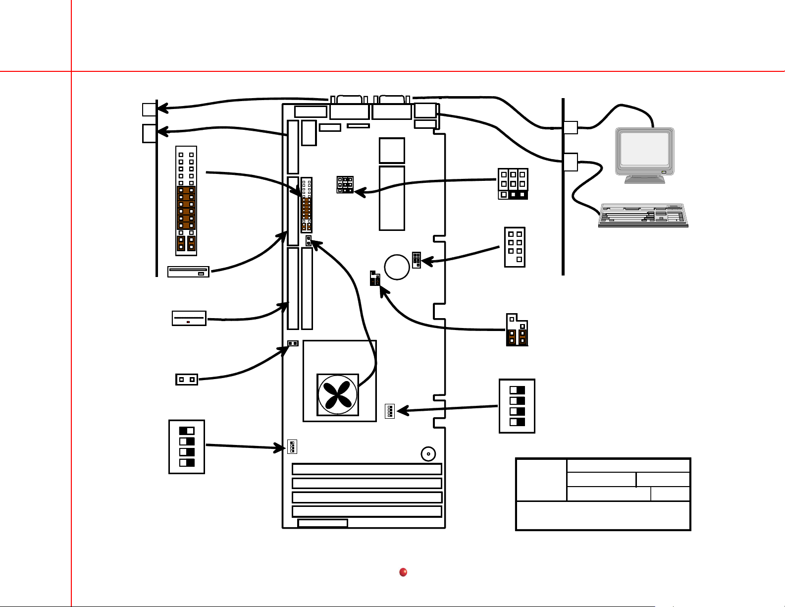
Functional Block 28 – Single Board Computer Connections / Jumpers (1 of 1) .......................................................................................... 31
Workstation
Contents
1
Page 2

Functional Block Diagrams Released 11/00
Functional Block 29 – Workstation Communications (1 of 15) ...................................................................................................................... 32
Functional Block 30 – Workstation Control Panel Processor Reset and Boot-up (2 of 15) ........................................................................ 33
Functional Block 31 – Workstation Control Panel Processor Reset Waveform (3 of 15) ............................................................................ 34
Functional Block 32 – Workstation Control Panel Key Board Interface (4 of 15) ......................................................................................... 35
Functional Block 33 – Workstation Control Panel IR Remote / Receiver Interface (5 of 15) ....................................................................... 36
Functional Block 34 – Workstation Control Panel Communication to System Interface (6 of 15) ............................................................. 37
Functional Block 35 – Workstation Control Panel Communication Waveforms (7 of 15) ........................................................................... 38
Functional Block 36 – Workstation System Interface Monitor Serial Communications (8 of 15) ............................................................... 39
Functional Block 37 – Workstation System Interface Monitor Serial Waveforms (9 of 15) ......................................................................... 40
Functional Block 38 – Workstation Touch Screen to System Interface Communication (10 of 15) ........................................................... 41
Functional Block 39 – Workstation Touch Screen to System Interface Waveforms (11 of 15)................................................................... 42
Functional Block 40 – Workstation Remote Diagnostic Interface (12 of 15)................................................................................................. 43
Functional Block 41 – Workstation System Interface Communications Overview 1 (13 of 15) .................................................................. 44
Functional Block 42 – Workstation System Interface Communications Overview 2 (14 of 15) .................................................................. 45
Functional Block 43 – Workstation Modem to System Interface Communications (15 of 15) .................................................................... 46
Functional Block 44 – System Interface I/O Map Select Lines (1 of 10)......................................................................................................... 47
Functional Block 45 – System Interface I/O External Relay Control 1 (2 of 10) ............................................................................................ 48
Functional Block 46 – System Interface I/O External Relay Control 2 (3 of 10) ............................................................................................ 49
Functional Block 47 – System Interface I/O Configuration Switch and ID (4 of 10) ..................................................................................... 50
Functional Block 48 – System Interface I/O External Cable ID (5 of 10) ........................................................................................................ 51
Functional Block 49 – System Interface I/O DS1, DS2 Diagnostic LEDs (6 of 10) ........................................................................................ 52
Functional Block 50 – System Interface I/O A/D Sense (7 of 10).................................................................................................................... 53
Functional Block 51 – System Interface I/O VCR Control (8 of 10) ................................................................................................................ 54
Functional Block 52 – System Interface I/O U1, U2 Diagnostic Display (9 of 10) ......................................................................................... 55
Functional Block 53 – System Interface I/O ARCNET, Quad UART, Option PROM (10 of 10)..................................................................... 56
Functional Block 54 – Image Path (1 of 7) ........................................................................................................................................................ 57
Functional Block 55 – Image Path Overview (2 of 7) ....................................................................................................................................... 58
Functional Block 56 – Image Path Info Video Controller PCB (3 of 7)........................................................................................................... 59
Functional Block 57 – Image Path out of Video Controller PCB (4 of 7)........................................................................................................ 60
Functional Block 58 – Image Path in Display Adapter PCB (5 of 7)............................................................................................................... 61
Functional Block 59 – Image Path in Display Controller PCB (6 of 7) ........................................................................................................... 62
Functional Block 60 – Image Path Waveforms (7 of 7) .................................................................................................................................... 63
Contents
2
Page 3

Functional Block Diagrams Released 11/00
Functional Block 61 – Pilot Tone (1 of 1) .......................................................................................................................................................... 64
Functional Block 62 – Frame Sync (1 of 1) ....................................................................................................................................................... 65
Functional Block 63 – CINE Option with CINE 2 Disk Backplane (1 of 3)...................................................................................................... 66
Functional Block 64 – CINE Option with CINE 4 Disk Backplane (2 of 3)...................................................................................................... 67
Functional Block 65 – CINE Bridge PCB Diagnostic LEDs (3 of 3) ................................................................................................................ 68
Functional Block 66 – Codonics Printer/Lenzar Camera (1 of 1).................................................................................................................... 69
Functional Block 67 – DICOM/DDPI (1 of 1) ...................................................................................................................................................... 70
Contents
3
Page 4
Functional Block Diagrams Released 11/00
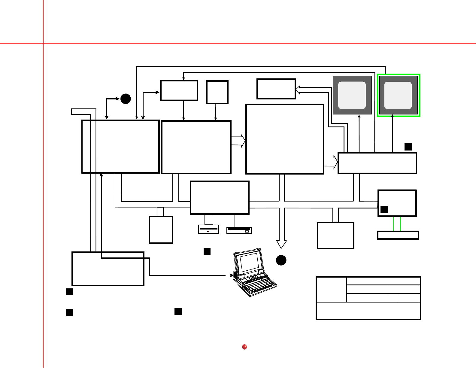
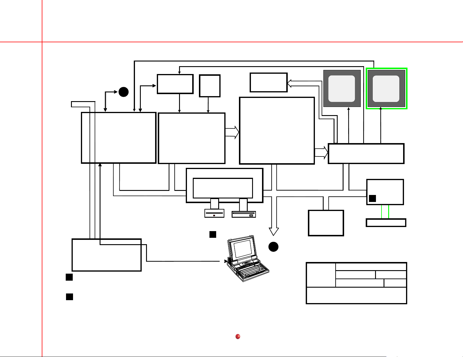
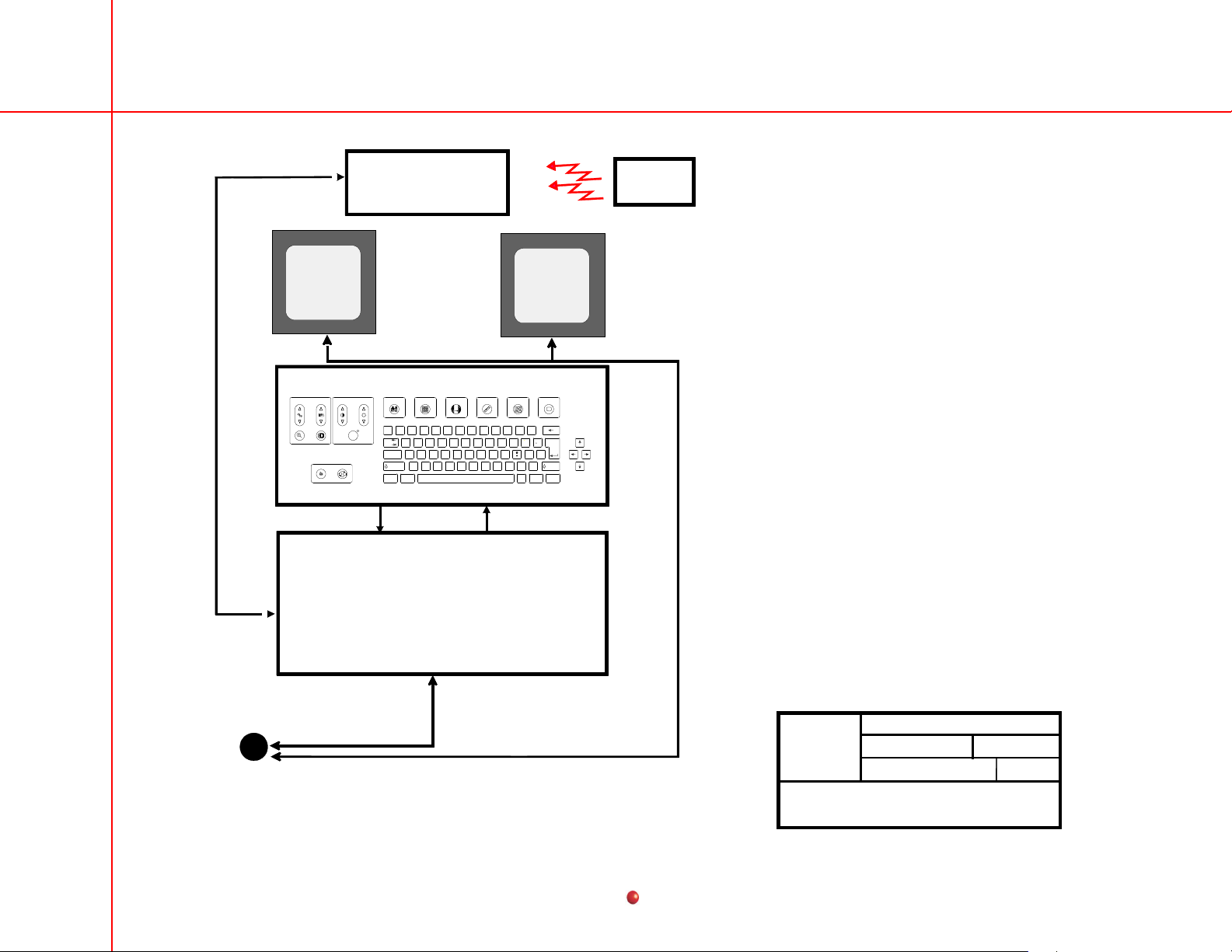
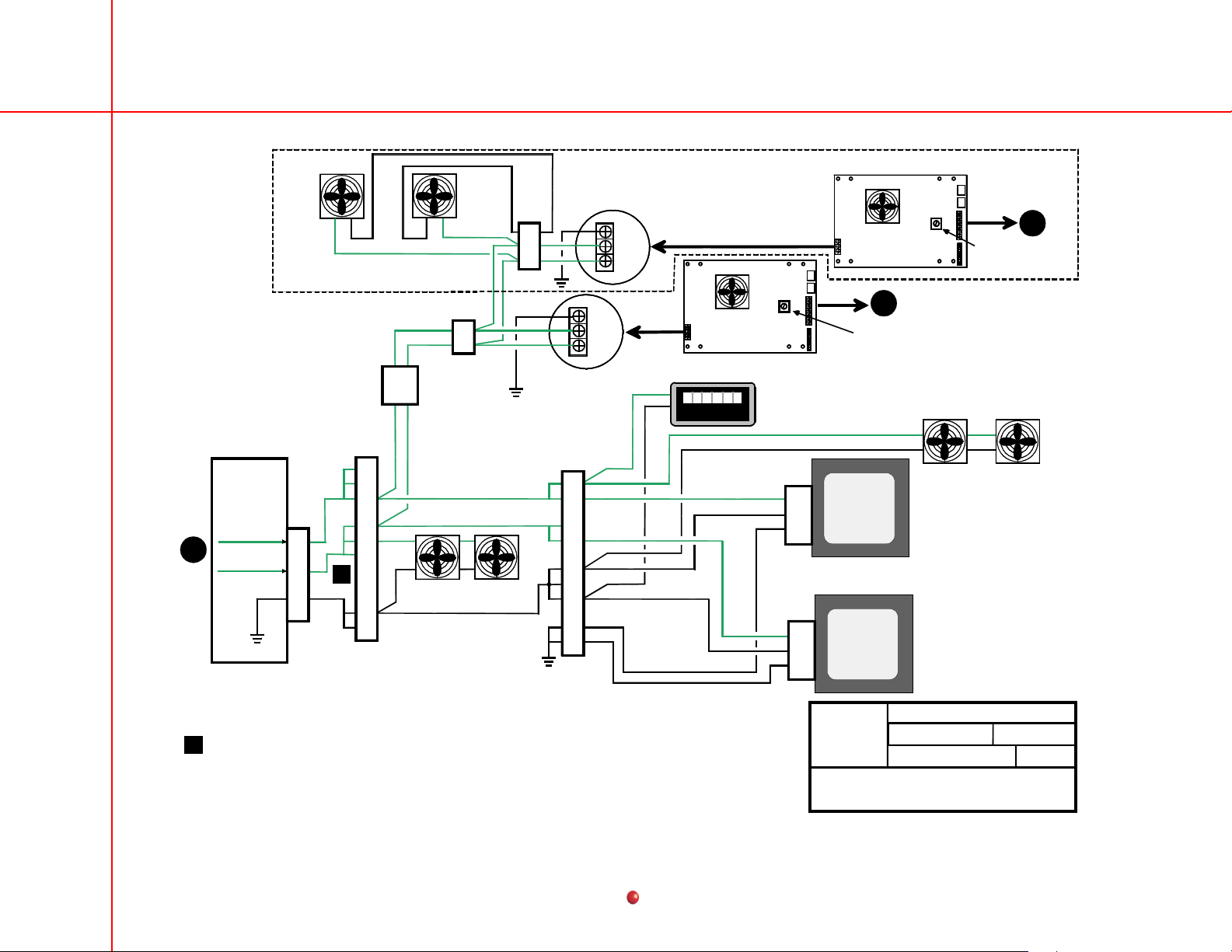
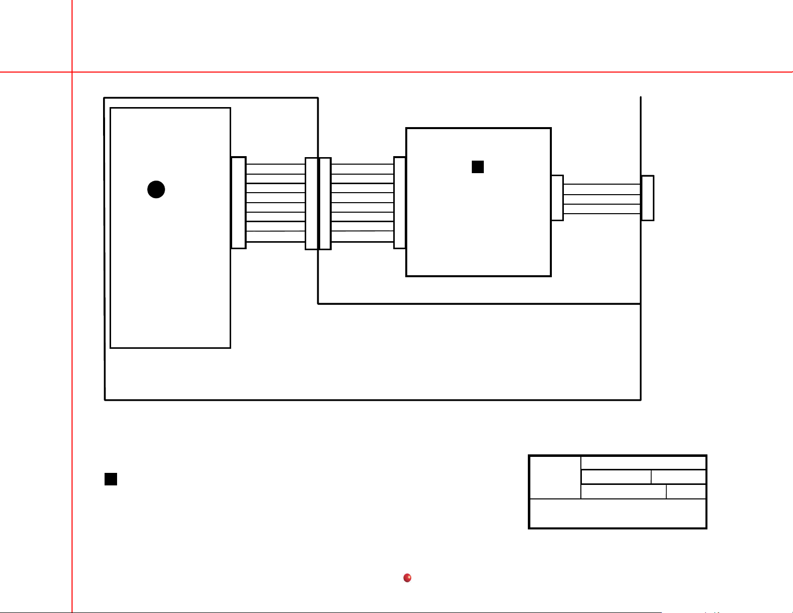
Serial Comm. to Touch Screen
Serial Comm. to
ARCNET
from C-Arm
Control Panel
and Monitors
2A
System Interface PCB
Option Prom
ARCNET Interlock
VCR Controls
Modem Interface
RS232 to Monitors
RS232 to Control Panel PCB
RS232 from Touch Screen
Control
VCR
Video Controller PCB
Pilot Tone Control
Anti Alias Filters
Anti Vignetting Circuits
Video A/D Converter
VLI Window for Generator ABS
ISA Bus
VGA
Card
External Interface PCB
External ARCNET Port
Room Interface Circuit
Power Injector Control Circuit
2.1 Gigabyte or larger Hard Drive
1
DOS readable C: Partition: 2.05 Gigabytes for image storage and data storage
Non DOS partition: 50 Megabytes for operating system and application software
SCSI Controller Card is located on PCI Bus 1
2
if CINE Option is installed. See page 3 of 6
Early systems may have a Display Controller PCB installed
3
which is functionally the same as the Display Adapter PCB
Video
from
CCD
Host Pentium
Processor
IDE Hard
Drive
1
Diagnostics
Lenzar Camera
or
Codonics Printer
Image Processor PCB
Vert. & Hor. Image Reversal
Circular Blanking
Window & Level Control
Automatic Sample Window Position
Real Time Edge Enhancement
Subtraction
Peak Opacification
Zoom & Roam
Text & Graphics
CINE Interface
1.44 Meg
Floppy
To CINE Option
3B
Touch Screen
Left & Right Video DAC to Monitors
PCI Bus 0
Ethernet Card
for DICOM
Option
LEFT
MONITOR
Interlace Video
Fast Scan Video
Display Adapter PCB
Interlace Video DAC to VCR
RIGHT
MONITOR
Fast Scan Video
SCSI Controller
Card
2
Jazz Drive
Early System Configuration
9800
Page 1 of 6
g
GE OEC Training
WSOV.DSF
Workstation System Overview
3
11/00
Functional Block 1 –Workstation Overview (1 of 6)
Contents
4
Page 5
Functional Block Diagrams Released 11/00
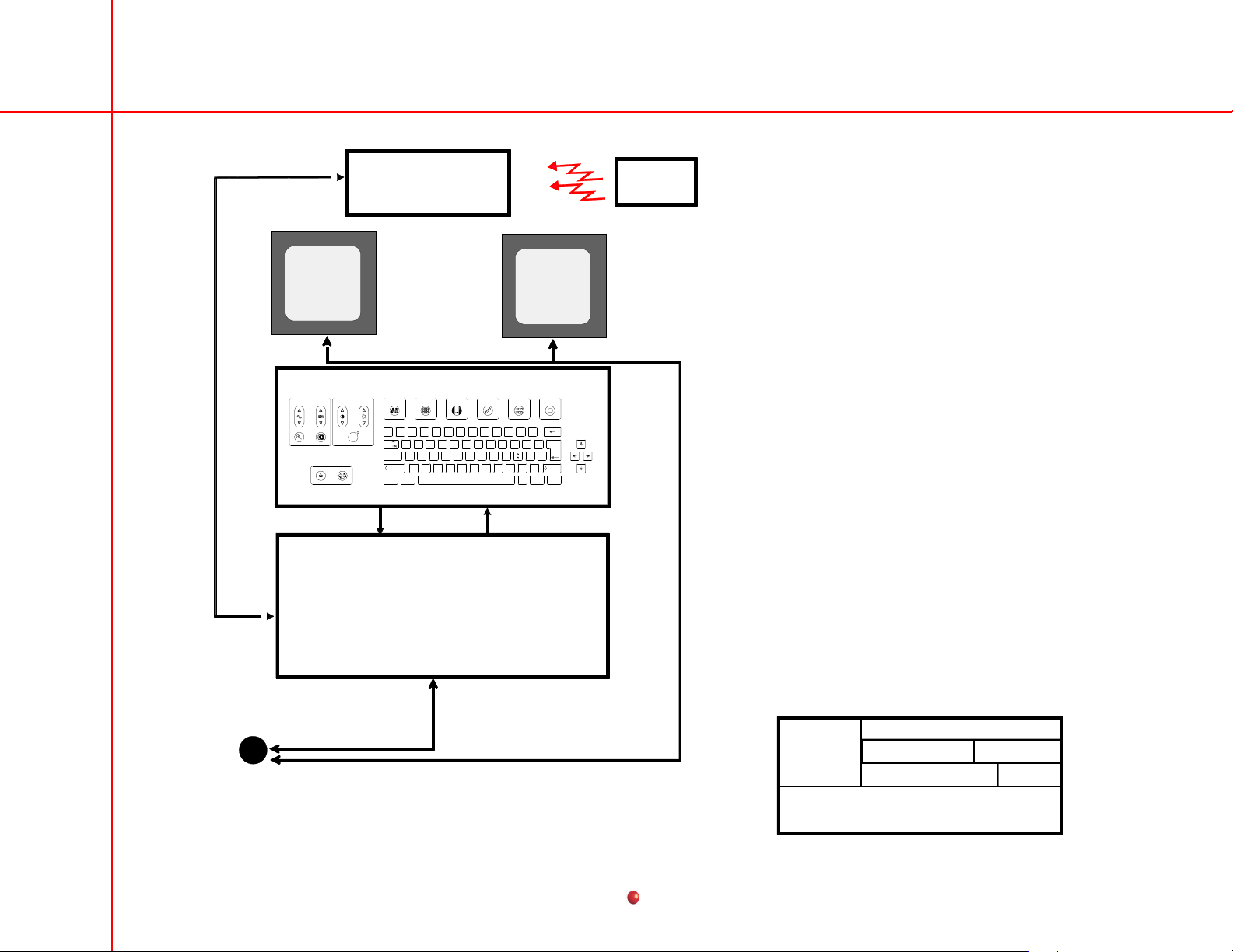
IR Receiver PCB
Coinverts IR Signals to TTL
Ambient Light Sensor
LEFT
MONITOR
Key Board Assy.
NOISEEDGE
ZOOM
NEGATE
SWAP
SAVE
PATIENT
BRIGHTNESS
!
?
/
AUTO
2@1
Q
Tab
A
Caps Lock
Z
Shift
IR Data to Control Panel Processor PCB
Control Panel Processor PCB
Switch Decode for the Key Board Assy.
Led Driver
IR Interface
Tone Generator
Serial Link to System Interface PCB
DIRECTORYINFORMATION
IMAGE
#
3EW5$4
Remote
Control
RIGHT
MONITOR
SPECIAL
IMAGE
ANNOTATIONCONTRASTFILTERENHANCE
%
^
6
R
Y
T
FD
VXSC
BGN
CUSTOMIZE
APPLICATIONS
(9*I)
&
8
7
U
JH
<,MK>
HELP
?
+=_
0
-
PO
~
'
/
L
Æ
Enter
¸
æ
"
Shift
\ß'
.
Del
Serial Comm. from
System Interface PCB
1A
Serial Brightness & Contrast Control to Monitors
Early System Configuration
g
Workstation System Overview
Control Panel Processor
Functional Block 2 – Workstation Overview (2 of 6)
Contents
9800
GE OEC Training
WSOV.DSF
Page 2 of 6
11/00
5
Page 6
Functional Block Diagrams Released 11/00
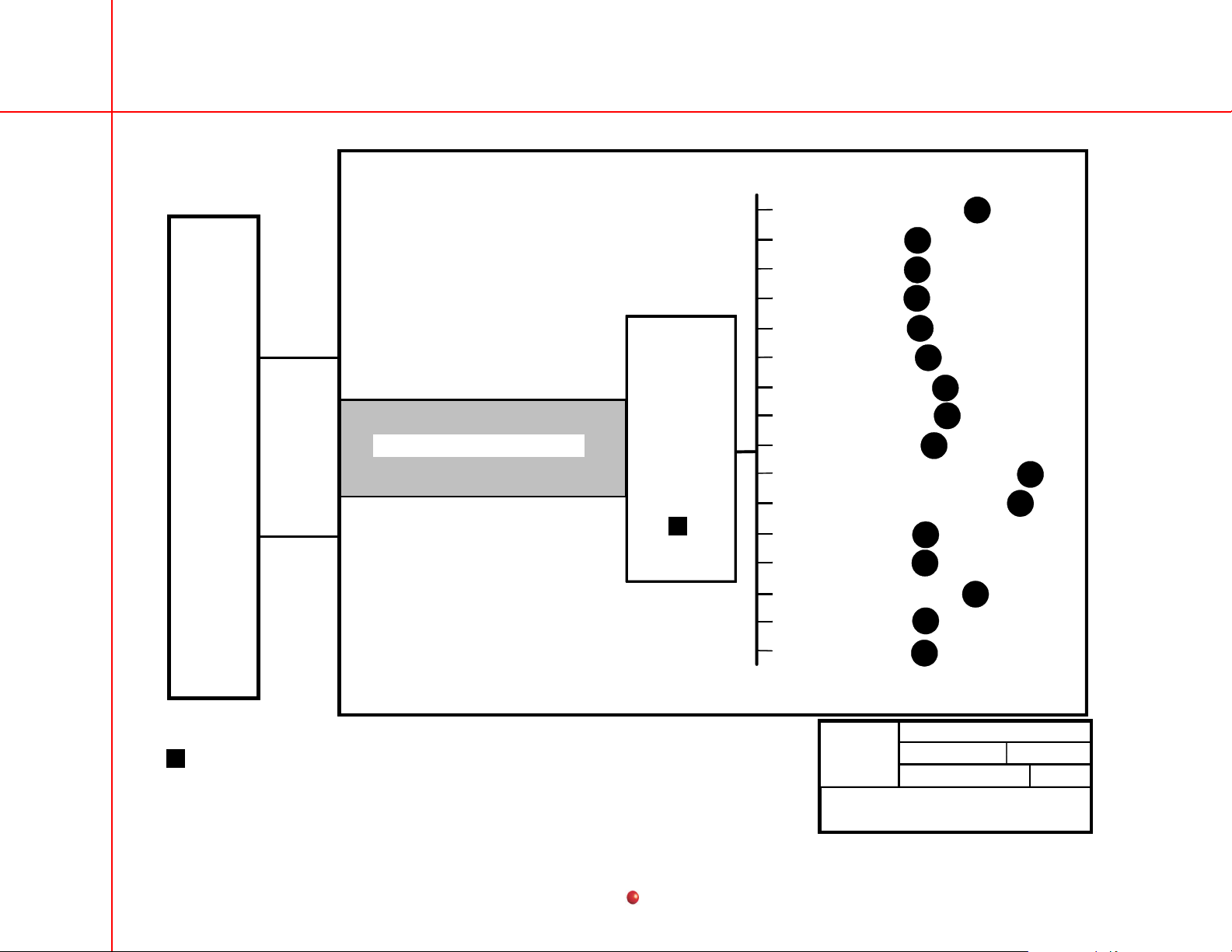
CINE Disk 1
CINE 2 Disk Backplane
Interface between
CINE Disks and the
Host Pentuim Processor
CINE Disk 2
2 Disk Option
15 FPS using
10 gigabyte drives
CINE Disk 3 CINE Disk 4
Disk Status
2
Fibre Channel Cable
CINE Bridge PCB
Frame Buffer seperating
PCI Bus 0 & PCI Bus 1
Fibre Channel Adapter
Interfaces PCI Bus 1 (Parallel)
& Fibre Channel (Serial)
CINE 4 Disk Backplane
Interface between
CINE Disks and the
Host Pentium Processor
4 Disk Option
30 FPS using
10 gigabyte drives
PCI Bus 1
CINE Disk 5 CINE Disk 6
SCSI Controller Card
1
Jazz Drive
SCSI Controller Card is located on PCI Bus 0
1
if CINE Option is not installed. See page 1 of 6.
The CINE 2 or CINE 4 Disk Backplane
2
will be connected to the CINE Bridge PCB
depending on system configuration.
1B
PCI Bus 0 from Host Pentium
g
Functional Block 3 – Workstation Overview (3 of 6)
Contents
Early System Configuration
9800
GE OEC Training
WSOV.DSF
Page 3 of 6
11/00
Workstation System Overview
Cine Options
6
Page 7
Functional Block Diagrams Released 11/00
Serial Comm. to Touch Screen
Serial Comm. to
ARCNET
from C-Arm
Control Panel
and Monitors
5A
System Interface PCB
Option Prom
ARCNET Interlock
VCR Controls
Modem Interface
RS232 to Monitors
RS232 to Control Panel PCB
RS232 from Touch Screen
Control
VCR
Video Controller PCB
Pilot Tone Control
Anti Alias Filters
Anti Vignetting Circuits
Video A/D Converter
VLI Window for Generator ABS
ISA Bus
External Interface PCB
External ARCNET Port
Room Interface Circuit
Power Injector Control Circuit
2.1 Gigabyte or larger Hard Drive
1
DOS readable C: Partition: 2.05 Gigabytes for image storage and data storage
Non DOS partition: 50 Megabytes for operating system and application software
SCSI Controller Card is located on PCI Bus 1
2
if CINE Option is installed. See page 6 of 6
Video
from
CCD
Passive Backplane
Host Pentium
Single Board Computer
W/ VGA Driver
IDE Hard
Drive
1
Diagnostics
Lenzar Camera
or
Codonics Printer
Image Processor PCB
Vert. & Hor. Image Reversal
Circular Blanking
Window & Level Control
Automatic Sample Window Position
Real Time Edge Enhancement
Subtraction
Peak Opacification
Zoom & Roam
Text & Graphics
CINE Interface
1.44 Meg
Floppy
To CINE Option
6B
Touch Screen
PCI Bus 0
Ethernet Card
for DICOM
Option
LEFT
MONITOR
Interlace Video
Fast Scan Video
Display Adapter PCB
Left & Right Video DAC to Monitors
Interlace Video DAC to VCR
RIGHT
MONITOR
Fast Scan Video
SCSI Controller
2
Jazz Drive
Current System Configuration
9800
GE OEC Training
g
WSOV.DSF
Workstation System Overview
Card
Page 4 of 6
11/00
Functional Block 4 – Workstation Overview (4 of 6)
Contents
7
Page 8
Functional Block Diagrams Released 11/00
IR Receiver PCB
Coinverts IR Signals to TTL
Ambient Light Sensor
LEFT
MONITOR
Key Board Assy.
NOISEEDGE
ZOOM
NEGATE
SWAP
SAVE
PATIENT
BRIGHTNESS
!
?
/
AUTO
2@1
Q
Tab
A
Caps Lock
Z
Shift
IR Data to Control Panel Processor PCB
Control Panel Processor PCB
Switch Decode for the Key Board Assy.
Led Driver
IR Interface
Tone Generator
Serial Link to System Interface PCB
DIRECTORYINFORMATION
IMAGE
#
3EW5$4
Remote
Control
RIGHT
MONITOR
SPECIAL
IMAGE
ANNOTATIONCONTRASTFILTERENHANCE
%
^
6
R
Y
T
FD
VXSC
BGN
CUSTOMIZE
APPLICATIONS
(9*I)
&
8
7
U
JH
<,MK>
HELP
?
+=_
0
-
PO
~
'
/
L
Æ
Enter
¸
æ
"
Shift
\ß'
.
Del
Serial Comm. from
System Interface PCB
4A
Serial Brightness & Contrast Control to Monitors
Current System Configuration
g
Workstation System Overview
Control Panel Processor
Functional Block 5 – Workstation Overview CPP (5 of 6)
Contents
9800
GE OEC Training
WSOV.DSF
Page 5 of 6
11/00
8
Page 9
Functional Block Diagrams Released 11/00
CINE Disk 1
Disk Status
CINE 2 Disk Backplane
Host Pentuim Processor
Fibre Channel Cable
CINE Bridge PCB
Frame Buffer seperating
PCI Bus 0 & PCI Bus 1
Fibre Channel Adapter
Interfaces PCI Bus 1 (Parallel)
& Fibre Channel (Serial)
CINE Disk 2
Interface between
CINE Disks and the
PCI Bus 1
2 Disk Option
15 FPS using
10 gigabyte drives
2 Disk Option
30 FPS using
18 gigabyte drives
SCSI Controller Card
1
Jazz Drive
4B
PCI Bus 0 from Host Pentium
SCSI Controller Card is located on PCI Bus 0
1
if CINE Option is not installed. See page 4 of 6.
Functional Block 6 – Workstation Overview Cine Options (6 of 6)
Contents
Current System Configuration
9800
Page 6 of 6
g
GE OEC Training
WSOV.DSF
Workstation System Overview
Cine Options
11/00
9
Page 10
Functional Block Diagrams Released 11/00
System Power Distribution
Incoming AC Power
(115 VAC)
Power Cord
External Circuit Breakers
CB1, CB2, CB3
Surge Suppressor
Isolation Transformer
Page 2
System Power Distribution
Incoming AC Power
(230 VAC)
Power Cord
External Circuit Breakers
CB1, CB2, CB3
Surge Suppressor
Isolation Transformer
Page 3
Power Control PCB
Power Distribution
Power Control PCB
Page 4
Key Power Control
Power Control PCB
Page 6
Workstation AC Power
Distribution
Page 7
Workstation DC
Distribution
Page 8
Cine 4 Power Distribution
Page 9
Floppy, CDR, Jazz, &
Mag. Opt. Drives
DC Power Distribution
Page 11
IDE Hard Drive,
Cine 2 Disk Backplane
DC Power Distribution
Page 12
System Interface,
External Interface
DC Power Distribution
Page 13
Image Processor,
Video Controller
DC Power Distribution
Page 14
Display Adapter,
CINE Bridge
DC Power Distribution
Page 15
Host CPU
DC Power Distribution
Page 16
Passive Backplane
DC Power Distribution
Page 17
Power Control PCB
Bad Line Voltage Sensing
Power Control PCB
Page 5
Control Panel Processor /
Touch Screen
DC Power Distribution
Page 10
g
Workstation Power Distribution
GE OEC Training
Functional Diagram Map
Functional Block 7 – Workstation Power Distribution (1 of 17)
Contents
9800
WSPD.DSF
1 of 17
11/00
10
Page 11
Functional Block Diagrams Released 11/00
CB1 (20A)
RESET ONLY
1
3
213
4
TB1
1-2
3-4
5-6
E1
91-128 VAC
Configuration
CB2 (10A)
RESET ONLY
2
4
DS1
1
J1
Surge Suppressor
00-876784
+24 Volt
Power
Supply
Voltage
Detector
Range
Switch
Overvoltage
Lockout
Comparitor
1
3
5
9
6
8
RV1
E1
RV2
RT2
RT1
E2
RT4
RT3
K1
5
6
7
3
1
8
Overvoltage
4
2
5
Lockout
Relay
RV4
RV3
J2
2
4
6
Power
Control
PCB
T1 - Isolation Transformer
2
125
113
1
5
E8
101
6
0
125
113
101
6
0
SHLD
E19
AC1
CT
AC2
AC
RTN
E4
CB4 (5A)
RESET ONLY
E4
E7
CB3 (10A)
RESET ONLY
230
VAC
P1
AC1_T1
4
3
AC2_T1
6
4A
2
5
5B
AC_T1
1
4
RTN_T1
3
115
VAC
DS1 turns on when the system is connected to facility power.
1
Strap T1 to match facility AC as follows:
2
Input VAC 91-98 98-104 104-110 110-116 116-122 122-128
T1 Taps 101/6 101/0 113/6 113/0 125/6 125/0
Functional Block 8 – System Power Distribution Incoming AC Power (2 of 17)
230 VAC
3
115 VAC
4
K1 will not energize if
5
the line voltage is
excessively high.
Contents
9800
2 of 17
11/00
g
GE OEC Training
WSPD.DSF
System Power Distribution
Incoming AC Power (115 VAC)
11
Page 12
Functional Block Diagrams Released 11/00
TB1
1-2
3-4
5-6
E1
182-256 VAC
Configuration
CB1 (10A)
RESET ONLY
1
3
2
4
DS1
1
J1
Surge Suppressor
Lockout
RV2
00-876784
RT2
RT1
E2
RT4
RT3
+24 Volt
Power
Supply
Voltage
Detector
Range
Switch
Overvoltage
Comparator
1
3
5
9
6
8
RV1
E1
K1
6
3
1
8
Overvoltage
5
7
4
2
5
Lockout
Relay
RV4
RV3
J2
2
4
6
Power
Control
PCB
T1 - Isolation Transformer
2
125
113
1
5
E8
101
6
0
125
113
101
6
0
SHLD
E19
AC1
CT
AC2
AC
RTN
E4
CB4 (5A)
RESET ONLY
E4
E7
CB3 (10A)
RESET ONLY
230
VAC
P1
AC1_T1
4
3
AC2_T1
6
4A
2
5
5B
AC_T1
1
4
RTN_T1
3
115
VAC
DS1 turns on when the system is connected to facility power.
1
Strap T1 to match facility AC as follows:
2
Input VAC 182-196 196-208 208-220 220-232 232-244 244-256
T1 Taps 101/6 101/0 113/6 113/0 125/6 125/0
Functional Block 9 – System Power Distribution Incoming AC Power (3 of 17)
230 VAC
3
115 VAC
4
K1 will not energize if
5
the line voltage is
excessively high.
Contents
9800
3 of 17
11/00
g
GE OEC Training
WSPD.DSF
System Power Distribution
Incoming AC Power (230 VAC)
12
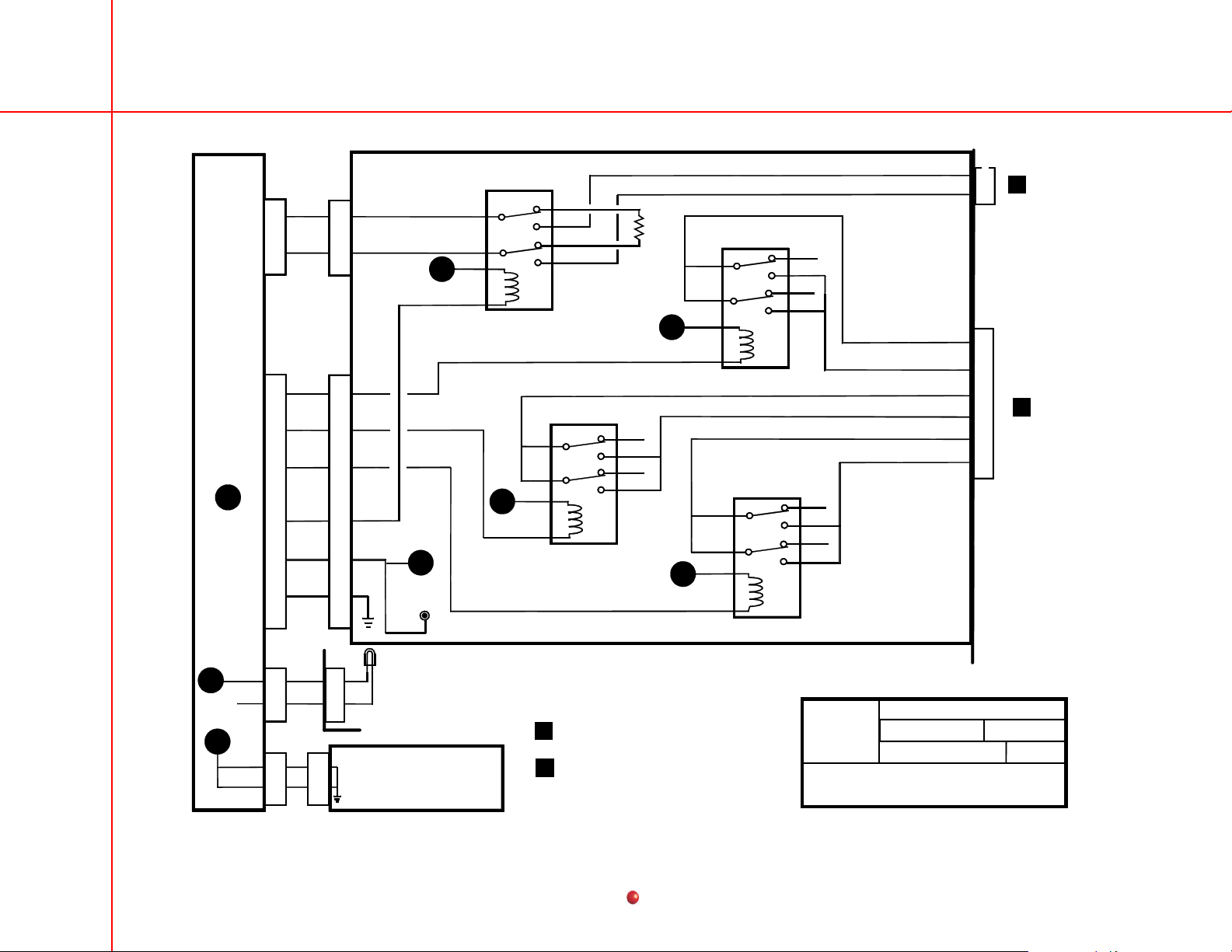
Page 13
Functional Block Diagrams Released 11/00
g
2A
3A
Power Control PCB
P1
5
1
3
AC_T1
RTN_T1
7
5
2
4
+12V
T1, CR1,
U1, C2
U2
9
14
Delay
Circuit
R1, R2,
C3, C5
R5
K3
13
12
Interconnect Plu
to C-Arm
See AC Power Distribution
Cable Assy
K4
6
3
8
1
CR4
8
TP2
TP1
1
2
4
7
5
8
1
See Key Power
LOOP1
LOOP2
3
6
Diagram
INT_GOOD_HI
INT_GOOD_LO
115VAC_PH
115VAC_RTN
CNCT_ON
P5
P2
1
4
2
6
5
3
1
4
00-879322
P6 J6
7 7
8 8
6H
System Interface PCB
J3
R8
3
8
1
2
16
Power Signal Interface PCB
Page 2 of 5
AC Power to C-Arm
VCC
U3
TIL117
K1
1
5
4
Arcnet / Serial
Communications
U13
ULN2803
2
See
Page 1 of 2
17
DS1
R10
LOOP1
LOOP2
J1
12
24
19
P1
12
6
6
9
9
24
19
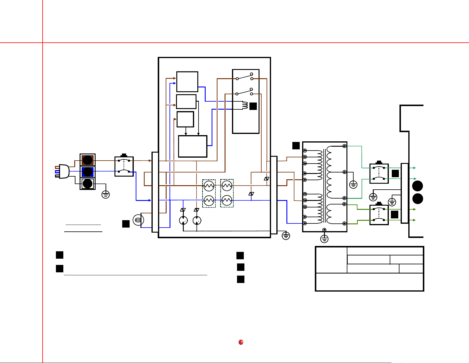
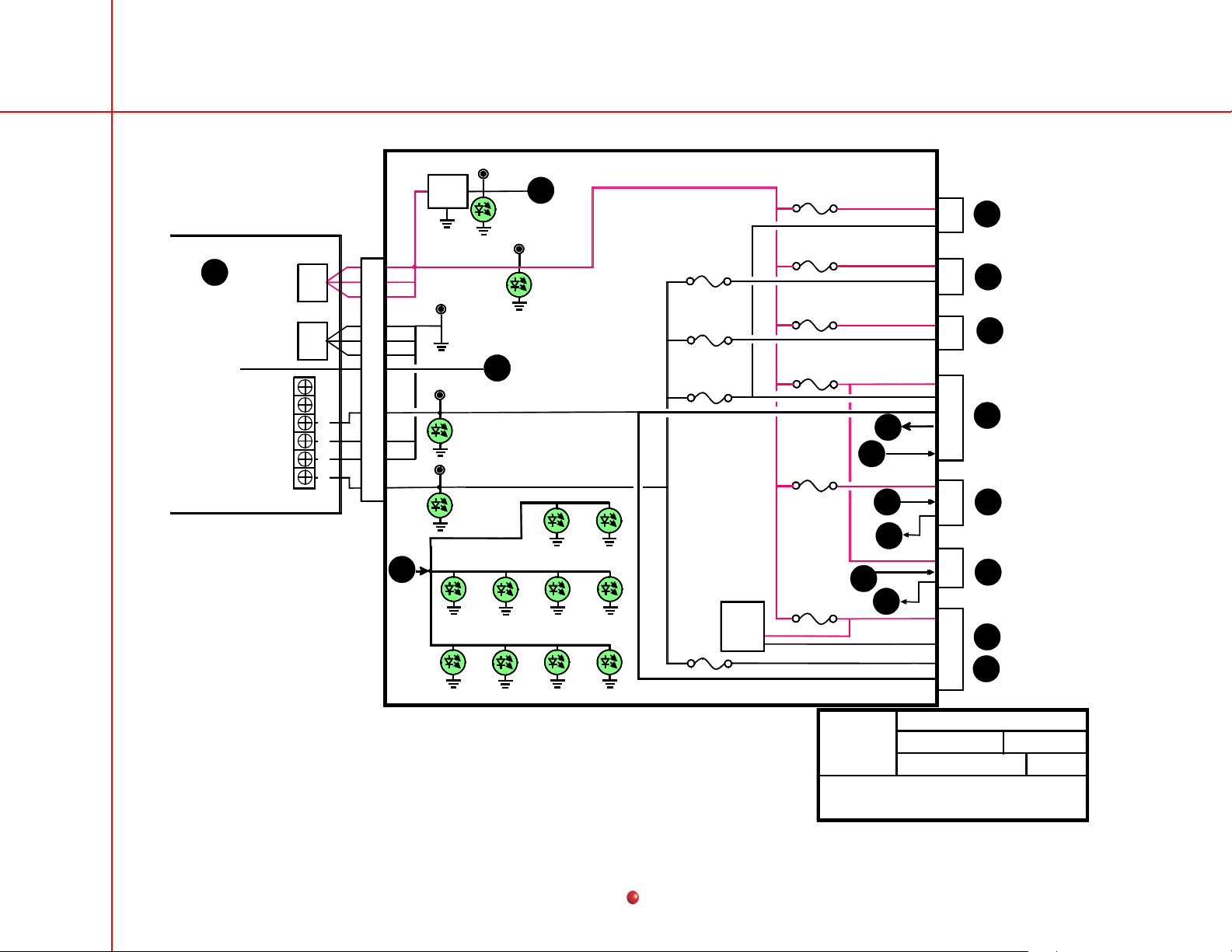
From Bad Line Voltage Alarm Circuit.
1
If the bad line voltage alarm is activated,
U2 pins 12 &13 will not go low,
preventing AC power from going to the generator
GE OEC Training
g
9800
WSPD.DSF
4 of 17
11/00
Power Control PCB Power Distribution
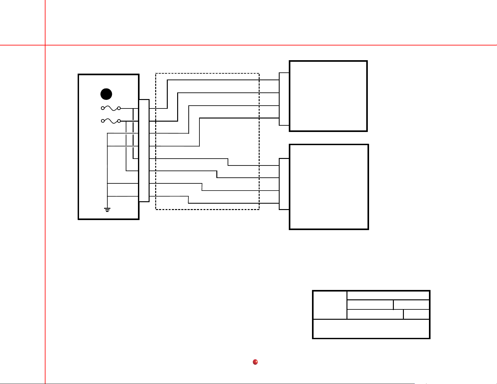
Functional Block 10 – Power Control PCB Power Distribution (4 of 17)
Contents
13
Page 14
Functional Block Diagrams Released 11/00
2B
3B
P1
4
6
2
AC1_T1
AC2_T1
CB1
200mA
7
5
2
4
Voltage Sensing Network
DS3
LINE HIGH
+12V
KEY_PWR
Power Control PCB
+12V Power Supply
T1, CR1, U1
K1
6
3
8
6F
1
DS2
LINE LOW
Voltage Sense Disable
Time Delay Networks
U3, Q5, Q6
DS1
PWR OK
TP5
+12V
E1
6G
1
6C
+12V
*RELAY_ON
Q1
Q3
CB2
200mA
K5
6
3
8
1
Bad Line Voltage
Alarm Circuit
Q7, Q8, CR12
R40, R41, R42
T2
AC1_CART
AC2_CART
7
5
2
4
LS1
10VAC
P6
Modem AC
1
Modem AC RTN
2
P4
1
4
2
P3
12V_KEY
1
2
3
4
7E
6D
1
2
MODEM
To Delay Circuit U2.
1
If the bad line voltage alarm is activated,
AC power is prevented from going to the generator
g
GE OEC Training
WSPD.DSF
Power Control PCB
Bad Line Voltage Sensing
Functional Block 11 – Power Control PCB Bad Line Voltage Sensing (5 of 17)
Contents
9800
5 of 17
11/00
14
Page 15
Functional Block Diagrams Released 11/00
ON /OFF
SWITCH
SW1
Power Control PCB
5D
P3
3
1
4
2
5
3
6
4
3
Power Control PCB
Bad Line Voltage
Sensing
3
K5
7
5
2
4
Bad Line Voltage
Alarm Circuit
See
5F
7
5
2
4
2
1
5C
6
3
TP5
8
1
K1
6
3
8
1
From
Delay Circuit
U2
5G
Sensing Network
+12V
T1, CR1,
U1, C2
From Voltage
4H
Interconnect Plug
P2
KEY_PWR
2
CNCT_ON
4
J1
14
22
P1
14
22
Backplane
P2
9
5
PCB
P4
6
18
Power Motor Relay PCB
Power Motor
Relay PCB
6
TP9
P1
14
15
Voltage to
PS1, PS2, PS3
See AC Power to
Page 4 of 6
8
1
TP2
K10
P7
12
7
5
6
6
3
Rear View
If relay K5 is energized by the Voltage Sensing Network,
1
5
4
Delay circuit U2 pin 14 disables AC Power to the C-Arm
Relay K1 shown in the de-energized condition.
2
3
Wire connections on the back of SW1:
Pin 3 White Pin 6 Black
Pin 5 Green Pin 4 Red
g
9800
GE OEC Training
WSPD.DSF
Key Power Control
6 of 17
11/00
Functional Block 12 – Key Power Control (6 of 17)
Contents
15
Page 16
Functional Block Diagrams Released 11/00
CINE 4 Disk Option Only
CINE
FAN 2
CINE
FAN 1
TB3
1
2
TB5
3
1
2
3
2
1
SK1
3
2
1
SK1
3
2
PS2
1
+
VE
-VE
6
5
4
3
2
3
2
PS1
1
1
1
2
3
4
5
6
7
8
8B
Voltage Adjustment
+VE
-V
E
6
5
4
3
2
1
1
2
3
4
5
Voltage Adjustment
6
7
8
9A
LF1
5E
Power
Control
PCB
AC1_CART
AC2_CART
P4
TB2
3
2
1
6
1
4
7
8
1
2
Fan B2
AC1
AC2
Fan B3
TB4
4
3
9
8
7
6
5
5
4
2
1
Lenzar Hardcopy Camera
connects to TB2
Codonics Printer
connects to TB4
With Arches option TB2 will have these additional power connections:
1
Tracker Computer Enclosure power to the attaches to TB2 pins 8 & 2.
Power Supply PS3 for Flat Panel Display attaches to TB2 pins 1 & 7.
Power Supply PS4 inside of Arches enclosure attaches to TB2 pins 8 & 2.
Ground connections to these power supplies are all attached to Ground connection E6 (not shown).
0 0 0 0 0 0
HOURS
1
/
10
P101
Fan B4 Fan B5
LEFT
3
MONITOR
1
5
P101
RIGHT
3
MONITOR
1
5
9800
7 of 17
11/00
g
GE OEC Training
WSPD.DSF
Workstation AC Power Distribution
Functional Block 13 – Workstation AC Power Distribution (7 of 17)
Contents
16
Page 17
Functional Block Diagrams Released 11/00
7B
+VE
+5V
PS1
Com
SK3 - 7
Power Fail
(NC)
(NC)
SK2
-12V
Com
Com
+12V
DS1 +3.3V from PS1 / VR1
DS2 -12V from PS1
DS3 +12V from PS1
DS4 +5V from PS1
DS5 sensed +5V from Vid. Cont.
DS6 sensed +3.3V from Vid. Cont.
DS7 sensed +5V from IP
DS8 sensed +3.3V from IP
-VE
6 5 4 3 2 1
VR1
+3.3V
P4
1
2
3
10
11
12
13
6
14
15
7
B
DS10 DS11
DS10 sensed +5V from Disp. Adapter
DS11 sensed +3.3V from Disp. Adapter
DS12 sensed +3.3V from Cine Bridge
DS13 sensed +5V from Cine Bridge
TP3
+3.3V
DS1
TP2
+5V
TP1
GND
C
TP5
-12V
DS2
TP4
+12V
DS3
DS5 DS6
DC Distribution PCB
A
DS4
DS14
DS7
DS12
DS15
DS8
DS13
5 A
F4
5 A
F7
1 A
F3
U1
Power
Monitor
5 A
F10
DS14 sensed +5V from CPP
DS15 sensed +12V from CPP
3.15 A
F6
5 A
F5
5 A
F8
6.3 A
F1
10 A
F2
10 A
F9
P1
P2
P3
P5
B
C
A
B
A
B
SYSRST*
g
P7
P8
P9
GE OEC Training
WSPD.DSF
Workstation DC Distribution
10C
11D
12E
13F
14H
15G
16I
17J
9800
8 of 17
11/00
Functional Block 14 – Workstation DC Distribution (8 of 17)
Contents
17
Page 18
Functional Block Diagrams Released 11/00
7A
PS2
SK2
+5V
Com
(NC)
(NC)
-12V
Com
Com
+12V
+VE
-VE
6 5 4 3 2 1
Cable Assy
00-879466
10 Amp
F1
P3
10
11
12
13
14
15
16
CINE 4 Disk Backplane
TP3
1
2
3
4
5
6
7
8
9
+5V
TP5
+12V
TP1, 2, 4, 6, & 7
GND
P3
P4
P5
P6
CINE Drive 3
CINE Drive 4
CINE Drive 5
CINE Drive 6
g
Functional Block 15 – Cine 4 Power Distribution (9 of 17)
Contents
9800
GE OEC Training
WSPD.DSF
9 of 17
Cine 4 Power Distribution
11/00
18
Page 19
Functional Block Diagrams Released 11/00
DC Distribution PCB
8C
3.15 A
1 A
F6
F3
J1
EMI Box
Cable Assy
00-879428
1
3
4
5
J1
EMI
11
12
30
19
17
18
35
Cable Assy
00-879475
+5V
+12V
GND
GND
+5V
+12V
GND
J1
2
4
3
5
P3
J1
1
Right Monitor
Touch Screen
9
6
Control Panel Processor PCB
TP14
+5V
TP4
+12V
+5V RTN
+12V RTN
TP1, 10, 8, 13
1
3
4
9800
GE OEC Training
g
WSPD.DSF
IR Reciever PCB
TP5
TP4
P1
4
1
6
Control Panel Processor / Touch Screen
DC Power Distribution
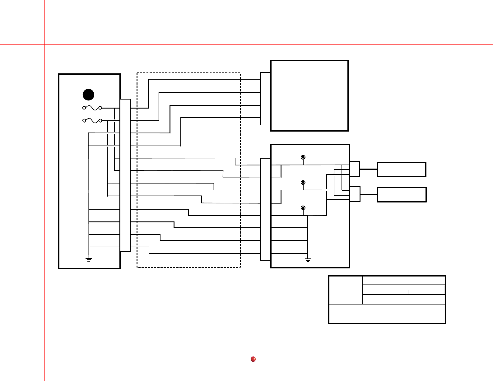
Functional Block 16 – Control Panel Processor Touch Screen DC Power Distribution (10 of 17)
Contents
10 of 17
11/00
19
Page 20
Functional Block Diagrams Released 11/00
DC Distribution PCB
8D
5 A
F5
1 A
F4
J1
2
Cable Assy
00-879430
1
3
6
7
4
8
9
+5V
+12V
GND
GND
+5V
+12V
GND
GND
J1
3.5" Floppy Disk Drive
1
4
2
3
J1
4
1
2
3
Jazz Drive
9800
GE OEC Training
g
WSPD.DSF
Floppy & Jazz Drives
DC Power Distribution
Functional Block 17 – Floppy & Jaz Drives DC Power Distribution (11 of 17)
Contents
11 of 17
11/00
20
Page 21
Functional Block Diagrams Released 11/00
DC Distribution PCB
8E
5 A
F8
5 A
F7
J3
10
11
12
Cable Assy
00-879427
1
4
7
8
2
3
5
6
9
+5V
+12V
GND
GND
+5V
+5V
+12V
+12V
GND
GND
GND
GND
J1
4
1
2
3
CINE Disk 2 Backplane
J3
1
2
3
4
5
6
7
8
IDE
Hard Disk Drive
TP1
TP2
TP3, 4, 5
J1
J2
CINE Drive 1
CINE Drive 2
9800
GE OEC Training
g
WSPD.DSF
IDE Hard Drive, Cine 2 Disk Backplane
DC Power Distribution
Functional Block 18 – IDE Hard Drive, Cine 2 Disk Backplane DC Power Distribution (12 of 17)
Contents
12 of 17
11/00
21
Page 22

Functional Block Diagrams Released 11/00
DC Distribution PCB
+5V
8F
+12V
15J 14J
SENSED VOLTAGES
SEE WORKSTATION
DC DISTRIBUTION
6.3 A
F1
1 A
F3
TP5
-12V
J5
25
26
27
28
29
30
22
23
1
31
32
33
34
Cable Assy
00-879432
System Interface PCB
J5
25
26
27
28
29
30
22
23
1
31
32
33
34
ADC
3
TP36
+5V
TP28
+12V
TP12
-12V
TP11, 3, 34, 23
GND
+12VMB
TP35
+5VMB
TP27
TP7
-12VMB
Cable Assy
00-879471
P11
15
16
2
17
18
1
10
12
14
16
14
External Interface PCB
P1
15
2
17
18
1
10
12
TP1
+5V
TP2
+12V
1
Room Interface
2
External Arcnet
See System Interface I/O
3
A/D Sense page 7 of 10
CB1
1.5A
TP3
GND
TP4
RELAY GND
P4
13
P3
10
15
2
8
5
1
SLOT 2
HOST PENTIUM CPU or
PASSIVE BACKPLANE
16A
See Host CPU DC Power Distribution
GE OEC Training
g
9800
WSPD.DSF
System Interface, External Interface
17A
See Host CPU DC Power Distribution
DC Power Distribution
Functional Block 19 – System Interface, External Interface DC Power Distribution (13 of 17)
Contents
13 of 17
11/00
22
Page 23

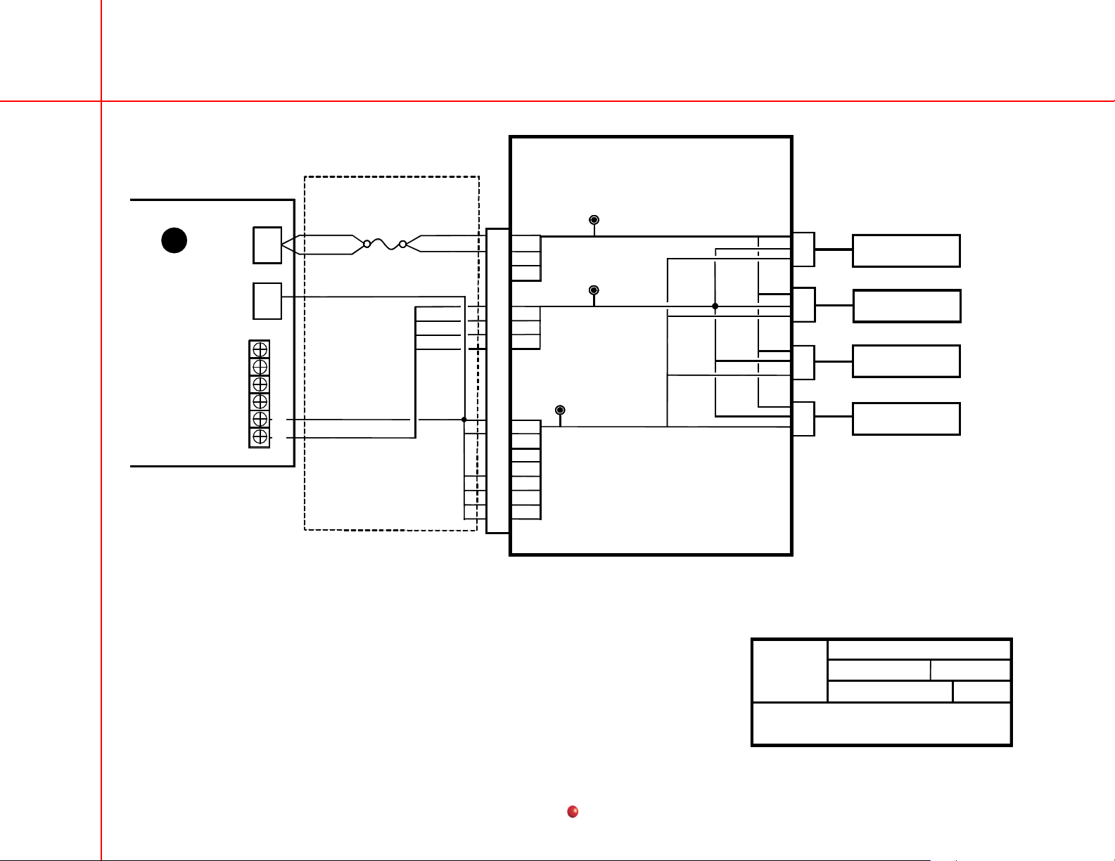
Functional Block Diagrams Released 11/00
DC Distribution PCB
+5V
TP3
+3.3V
TP1
GND
8H
SENSED VOLTAGES
SEE WORKSTATION
DC DISTRIBUTION
10 A
F2
13J
J7
14
15
10
11
12
13
17
18
Cable Assy
00-879429-01
1
2
3
4
P7
2
6
3
7
5
8
1
4
P3
2
6
3
7
5
8
1
4
Video Controller PCB
TP20
+5V
TP22
+3.3V
TP11
GND
+5V SENSE
+3.3V SENSE
Image Processor PCB
TP1
+5V
TP2
+3.3V
TP7
GND
+5V SENSE
+3.3V SENSE
U56
3.3V
TP58
+5V Analog
TP59
-5V Analog
TP74
+5VMB
U60
7805
U62
7905
TP56
ISA Gnd
TP11
PCI +5V
PCI +3.3V
PCI Gnd
ISA +5V
ISA +12V
ISA -12V
SLOT 1
ISA Gnd
SLOT 6
PCI +5V
PCI +3.3V
PCI Gnd
HOST
PENTIUM
CPU
or
PASSIVE
BACKPLANE
16A
17A
9800
GE OEC Training
g
WSPD.DSF
Image Processor, Video Controller
DC Power Distribution
Functional Block 20 – Image Processor, Video Controller DC Power Distribution (14 of 17)
Contents
14 of 17
11/00
23
Page 24

Functional Block Diagrams Released 11/00
DC Distribution PCB
+5V
TP3
+3.3V
TP1
GND
SENSED VOLTAGES
SEE WORKSTATION
DC DISTRIBUTION
6.3 A
F1
8G
13J
J8
12
13
17
18
14
15
1
2
3
4
10
11
Cable Assy
00-879429-02
P2
2
6
3
7
5
8
1
4
P3
2
6
3
7
5
8
1
4
Display Adapter PCB
+5V SENSE
+3.3V SENSE
CINE Bridge PCB
TP2
VCC
+3.3V
TP7
GND
+5V SENSE
+3.3V SENSE
U1
3.3V
TP23
+5V
U33
3.3V
and
1
2.5V
TP46
+12V
TP45
-12V
TP15
GND
PCI +5V
PCI 3.3V
PCI +12V
PCI -12V
PCI Gnd
SLOT 5
HOST
PENTIUM
TP3
3.3V
TP18
3.3V
TP17
TP19
TP10
U48
TP20
+3.3V
TP21
PCI Gnd
PCI +5V IO
PCI +5V
SLOT 7
PCI +3.3V
PCI +12V
PCI -12V
PCI Gnd
CPU
or
PASSIVE
BACKPLANE
The Display Controller PCB uses a 3.3 volt regulator only.
1
The Display Adapter PCB can ues a 3.3volt and a 2.5 Volt regulator.
The 2.5 volt regulator voltage is not sensed by the System Interface PCB.
Functional Block 21 – Display Controller, Cine Bridge DC Power Distribution (15 of 17)
Contents
16A
17A
9800
GE OEC Training
g
WSPD.DSF
Display Controller, Cine Bridge
DC Power Distribution
15 of 17
11/00
24
Page 25

Functional Block Diagrams Released 11/00
VIDEO CONTROLLER PCB SLOT 1
SYSTEM INTERFACE PCB SLOT 2
DC Distribution PCB
+12V
+5V
5 A
F10
TP5
-12V
U1
Power
Monitor
10 A
F9
8I
LASER CAMERA PCB SLOT 3
VGA VIDEO PCB SLOT 4
Cable Assy
J9
6
13
1
5
7
9
10
8
2
3
4
11
12
00-879431-02
FAN 1 +12V
FAN 2 GND
+5V
+12V
-12V
GND
GND
RESET*
+5V
+5V
+5V
GND
GND
J1
J2
ISA BUS
A1
1
2
2
3
4
5
6
1
4
5
6
1
2
HOST
PENTIUM
CPU
13A 14A
PCI BUS 0
SLOT 5 DISPLAY CONTROLLER PCB
o
SLOT 6 IMAGE PROCESSOR PCB
SLOT 7 CINE BRIDGE PCB OR
SCSI CONTROLLER PCB
SLOT 8 ETHERNET PCB
1.44 Meg
Floppy
IDE Hard
Drive
g
DC Power Distribution
Functional Block 22 – Host CPU DC Power Distribution (16 of 17)
Contents
9800
GE OEC Training
WSPD.DSF
Host CPU
16 of 17
11/00
25
Page 26
Functional Block Diagrams Released 11/00
VIDEO CONTROLLER PCB SLOT 1
SYSTEM INTERFACE PCB SLOT 2
SINGLE BOARD COMPUTER PCI / ISA SLOT
DC Distribution PCB
+12V
+5V
5 A
F10
TP5
-12V
U1
Power
Monitor
10 A
F9
8I
LASER CAMERA PCB SLOT 3
PCI / ISA SLOT (SPARE)
J9
6
13
1
5
7
9
10
8
2
3
4
11
12
+5V
+12V
-12V
GND
GND
RESET*
+5V
+5V
+5V
GND
GND
J1
J2
ISA BUS
2
3
4
5
6
1
4
5
6
1
2
PASSIVE
BACKPLANE
00-901697-01
13A 14A
PCI BUS 0
SLOT 5 DISPLAY CONTROLLER PCB
o
SLOT 6 IMAGE PROCESSOR PCB
SLOT 7 CINE BRIDGE PCB OR
SCSI CONTROLLER PCB
SLOT 8 ETHERNET PCB
1
1.44 Meg
Floppy
1
IDE Hard
Drive
1
See Single Board Computer Functional Diagram.
Functional Block 23 – Passive Backplane DC Power Distribution (17 of 17)
Contents
g
9800
GE OEC Training
WSPD.DSF
Passive Backplane
DC Power Distribution
17 of 17
11/00
26
Page 27

Functional Block Diagrams Released 11/00
P4
1
2
9
7
6
R1
150
9
8
VCC
CONFIG 0
DIAG_RXD
DIAG_TXD
2
EXTERNAL
INTERFACE PCB
00-879184
REAR
PANEL
K1
Laptop
running
RUT
13
4
+12V
ISOLAT_RLY_CNTL
P2
26
22 22
20
19
P1
P4
1
2
26
20
19
P11
SYSTEM INTERFACE PCB
00-879054
ARCNET_HI
1
ARCNET_LO
2
BD4
4
TRANSCEIVER
U20
61
42018
7
TRANSCEIVER
RS485
REMOTE DIAGNOSTICS NODE
13
4
3
U7
6
1420
7
18
RS485
U36
DATA(15..0)
DIAGNOSTIC
ARCNET
CONTROLLER
DIAG_RXD
DIAG_TXD
K1
PENTIUM
ARCNET
CONTROLLER
R2
150
9
8
INT_GOOD_HI
INT_GOOD_LO
U37
BD(7..0)
U43
DIAGNOSTIC
PROCESSOR
MC68HC16Z1
18
17
DIAGNOSTIC LEDS
DS1 DS2
U32
8
14
11
7
U1
00
12
24
22
6
9
2
35413
STATUS
LEDS
U46
U16
U2
19
21
P3
1
2
3
8
P12
3
2
EMI
Interconnect
BOX
J6
P6
ARCNET_HI
1
1
ARCNET_LO
2
2
7
7
8
8
5
POWER
CONTROL
1
PCB
00-880315
MOD_TXD
MOD_RXD
MODEM
WORKSTATION
Cable
6
J1
7
8
P2
SLOT 2
HOST PENTIUM CPU or
PASSIVE BACKPLANE
See Power Control PCB Power Distribution
1
Page 4 of 16
2
See Workstation Remote Diagnostics Interface Page 8 of 11
Shown in Workstation Standalone condition. Activated by CNCT_ON circuit.
3
See Power Control PCB Power Distribution Page 4 of 16.
Diagnostic Processor U43 monitors the CONFIG 0 line and activates Relay K1 on the External Interface PCB
4
using the BD4 line when an external ARCNET cable is attached.
Functional Block 24 – ARCNET Communications (1 of 4)
Contents
GE OEC Training
g
ARC_NET.DSF
Arcnet Communications
Functional Diagram
9800
Page 1 of 4
11/00
27
Page 28

Functional Block Diagrams Released 11/00
P1
ARCNET_HI
7
ARCNET_LO
8
INTERCONNECT
CABLE
J2
A3
P1
RS485
TRANSCEIVER
TP6
TP7
17
18
TP4
Y2
TP35
20
MHz
TP37
TP18
Y1
20
MHz
TP44
TRANSCEIVER
TP39
6
2
A2
P1
17
18
FLUORO FUNCTIONS PCB
00-879099
TP5
24
ARC_INT*
6
7
DATA(15..0)
U10
U5
ARCNET
CONTROLLER
XRAY CONTROLLER PCB
RS485
6
7
U55
ARCNET
CONTROLLER
U30
00-879803
TP15
24
SD(15..0)
INT_*ARC
DIAGNOSTIC LEDS
DS1
STATUS
LEDS
U5
0
U1
5
U25
SD BUFFER
U6
STATUS
0
LEDS
DS2
U2
PROCESSOR
MC68HC16Z1
0
D(31..16)
U36
MICRO
U21
MICRO
PROCESSOR
DIAGNOSTIC
LEDS
U57
U58
486
DS 1-5
P1
1
1
A1
HIGH VOLTAGE SUPPLY REG. PCB
BACK
P1
PLANE
C-ARM
1
See Control Panel & Fluoro Functions Communications Diagram Page 3 of 3
00-879362
00-878727
ARCNET
NOT USED
ON THIS PCB
Functional Block 25 – ARCNET Communications (2 of 4)
Contents
GE OEC Training
g
ARC_NET.DSF
Arcnet Communications
Functional Diagram
9800
Page 2 of 4
11/00
28
Page 29
Functional Block Diagrams Released 11/00
TP44
TP6
TP7
TP5
GND
TP4
U2
U1
DS2
Y2
TP5
ARC_INT*
2 V/div dc
2 ms/div
1
TP5
ARC_INT*
2 V/div dc
0
4
5 s/div
2
5
TP6
ARCNET_LO
1 V/div dc
2 us/div
Fluoro Functions PCB
DS1
3
Active condition, buttons pressed on Control Panel.
1
Idle condition, no buttons pressed on Control Panel.
2
3
Segment 6 on DS1 blinks at 1Hz rate when Fluoro Functions Micro Controller is running.
OE
The code displayed on U1-U2 is
4
when ARCNET communication is lost.
Functional Block 26 – ARCNET Communications Fluoro Functions Waveforms (3 of 4)
Contents
TP7
ARCNET_HI
1 V/div dc
2 us/div
9800
Page 3 of 4
g
GE OEC Training
ARC_NET.DSF
Arcnet Communications
Fluoro Functions Waveforms
11/00
29
Page 30

Functional Block Diagrams Released 11/00
X-Ray Controller PCB
TP15
INT_ARC*
2 V/div dc
20 Ms/div
1
TP37
TP39
GND
1
2
ARCNET failed condition.
3
The code displayed on U5-U6 is
TP35
TP15
Idle condition, no buttons pressed on the Control Panel. ARCNET OK.
00
representing normal operation.
DS1
DS2
DS3
DS4
DS5
U5
U6
0
0
3
TP15
INT_ARC*
2 V/div dc
200 Ms/div
2
TP37
ARCNET_LO
1 V/div dc
2 us/div
TP35
ARCNET_HI
1 V/div dc
2 us/div
9800
g
GE OEC Training
ARC_NET.DSF
Page 4 of 4
11/00
Arcnet Communications
X-Ray Controller Waveforms
Functional Block 27 – ARCNET Communications X-ray Controller Waveforms (4 of 4)
Contents
30
Page 31
Functional Block Diagrams Released 11/00
Com 1
RS232
LPT1
P8
J9
8
6
4
2
Rear Panel
1.44 Meg
IDE Hard
J7
28
26
24
22
20
18
16
14
12
10
Floppy
Drive
JP6
open
SW1
ON
27
25
23
21
19
17
15
13
11
9
7
5
3
1
1 2 3 4
Power
Parallel Port
P1
J10
J9
J5
Floppy Drive
J3 J4
Primary IDE
JP6
SW1
1 2 3 4
ON
Com Port
J13
J11
JPW3
JPW2
JPW4
JPW1
J7
J6
CPU fan power
Secondary IDE
Socket 7
233 mHz MMX
Processor
SIMM 4 empty
SIMM 3 empty
SIMM 2
SIMM 1
J1
J14J12
VGA Port
KB
Ctrl
BIOS
J18
JP5
Bat1
SW3
1 2 3 4
ON
J16
J15
J19
J20
BZ1
Key board
3
JPW2
JPW1
4
1
Service
JPW
Monitor
JPW4
4
Service Keyboard
1
Rear Panel
J20
J19
J18
JP5
1 2 3
1
SW3
1 2 3 4
ON
9800
GE OEC Training
g
SBC.DSF
Single Board Computer
Connections / Jumpers Diagram
Page 1 of 1
11/00
Functional Block 28 – Single Board Computer Connections / Jumpers (1 of 1)
Contents
31
Page 32

Functional Block Diagrams Released 11/00
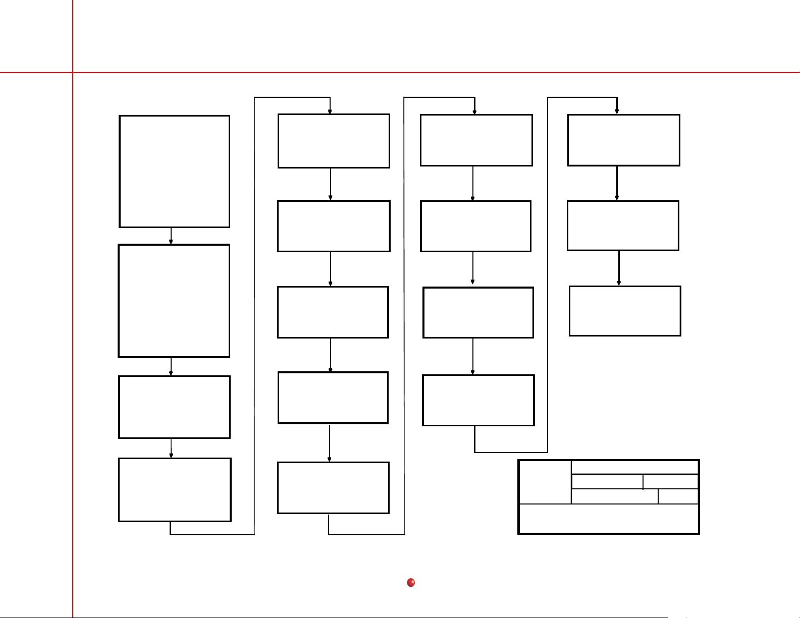
Workstation Control Panel
Processor Reset & Bootup
Page 2 of 15
Workstation Control Panel
IR Remote / Receiver Interface
Page 5 of 15
Workstation System Interface
Monitor Serial Communications
Page 8 of 15
Workstation Touch Screen to
System Interface Waveforms
Page 11 of 15
Workstation Control Panel
Processor Reset Waveform
Page 3 of 15 Page 4 of 15
Workstation Control Panel
Communication to System Interface
Page 6 of 15
Workstation System Interface
Monitor Serial Waveforms
Page 9 of 15
Workstation
Remote Diagnostics Interface
Page 12 of 15
Workstation Control Panel
Key Board Interface
Workstation Control Panel
Communication Waveforms
Page 7 of 15
Workstation Touch Screen to
System Interface Communications
Page 10 of 15
Workstation System Interface
Communications Overview 1
Page 13 of 15
Workstation System Interface
Communications Overview 2
Page 14 of 15
Functional Block 29 – Workstation Communications (1 of 15)
Workstation Modem to
System Interface Communications
Page 15 of 15
Contents
9800
Page 1 of 15
g
GE OEC Training
WSSCOM.DSF
Workstation Communications
Functional Diagram Map
11/00
32
Page 33
Functional Block Diagrams Released 11/00
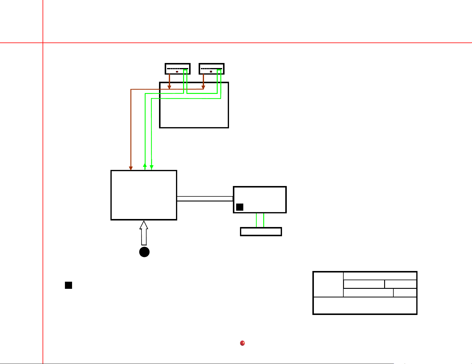
See Control Panel /
Touch Screen
DC Power Distribution
Page 10 of 16
+5V
+12V
GND
GND
Control Panel
Processor PCB
00-876611
J1
2
4
3
5
TP14
+5V
TP4
+12V
+5V RTN
+12V RTN
AD0 - AD15
TP1, 10,
8, 13
U14,U2
ADDRESS
DECODE
74ABT573
U1
Static
Ram
U5
80C196KC
Micro
Controller
Latched Add. 0 - 15
U10
Boot
Prom
HSO.0
OSC
P1.1
RESET
28
TP11
5
12 MHZ
20
6
1
TP12
16
2
U4
Add. Decode
PAL
7
13 12
2
U11
Y1
U24
MAX694
(Power Monitor &
Watchdog Timer)
U11
2 1 6 5
4A
U13
L239
Driver
VCC
2
7
P7
6
3
2
1
Externally
Mounted
1
Resets Watchdog timer every 3 ms.
TP12 is High under nornal conditions.
2
TP12 will go Low causing U5 to be reset if VCC drops below 4.65 volts,
or if the watchdog timer reset pulses are lost.
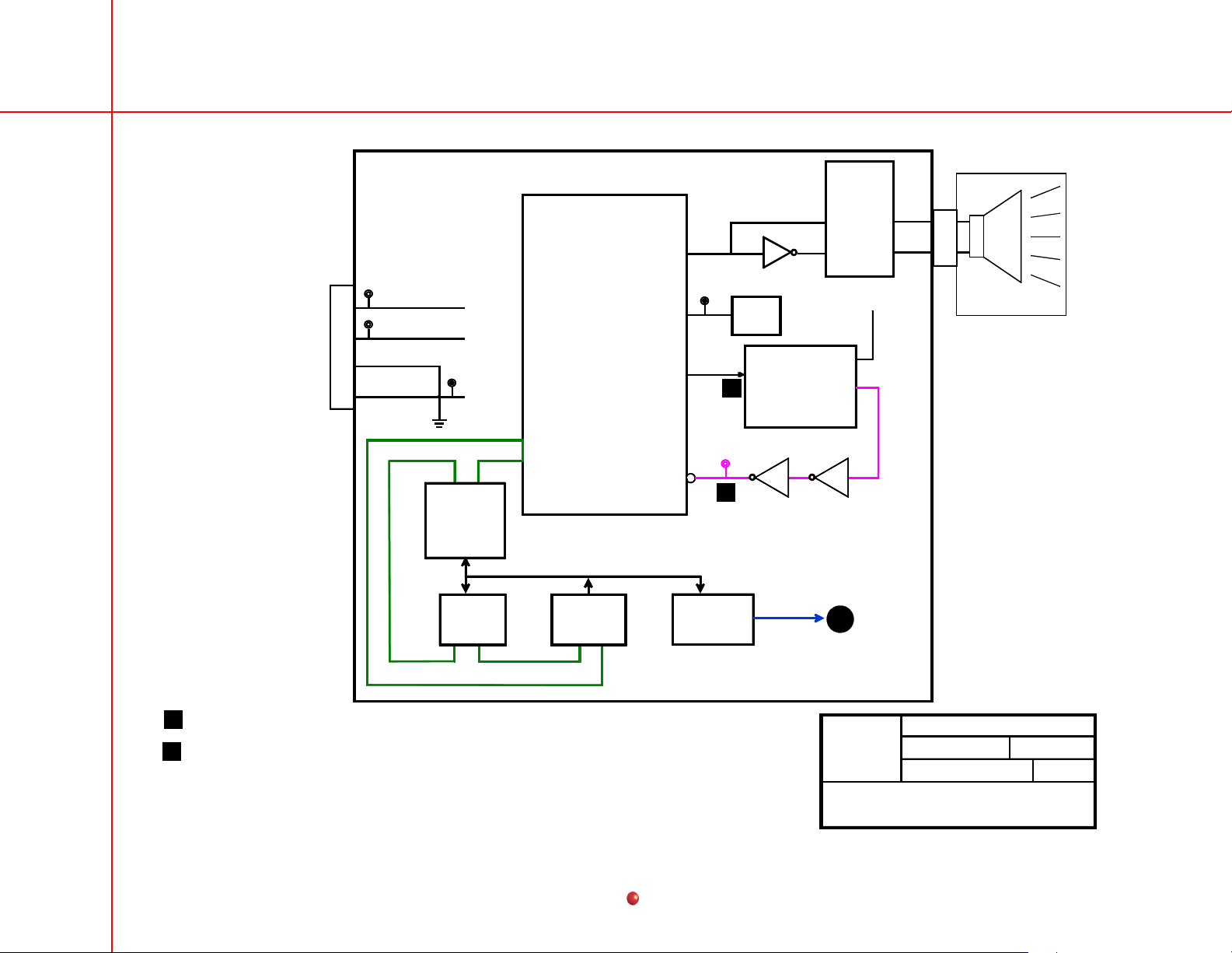
Functional Block 30 – Workstation Control Panel Processor Reset and Boot-up (2 of 15)
Contents
9800
GE OEC Training
g
WSSCOM.DSF
Workstation Control Panel
Processor Reset & Bootup
Page 2 of 15
11/00
33
Page 34

Functional Block Diagrams Released 11/00
U2
U1
U10
U4
U14
TP1
DS1 DIAGNOSTIC LED
CONTROL PANEL PROCESSOR
1
6
TP13
ASSY 00-876613
U5
Y1
TP10
TP14
U11
TP11
6
TP4
TP12
U24
P1
U13
TP8
P7
U24-6
2 V/div dc
1 ms/div
Segment 6 indicates the alarm is being driven.
1
Functional Block 31 – Workstation Control Panel Processor Reset Waveform (3 of 15)
Contents
9800
GE OEC Training
g
WSSCOM.DSF
Workstation Control Panel
Processor Reset Waveform
Page 3 of 15
11/00
34
Page 35

Functional Block Diagrams Released 11/00
Control Panel
Processor PCB
00-876611
U5
80C196KC
Micro
Controller
2A
U4
Add. Decode
PAL
AD0 - AD15
DIAG_DISPLAY_WR
LED_WR
COL_READ
ROW_DRV
U20, U21
DIAGNOSTIC
LED
LATCH
U16
CONTROL PANEL
LED LATCH
U15, U23
KEY BOARD
INPUT LATCH
(COLUMN READ)
U18, U22
KEY BOARD
OUTPUT LATCH
(ROW DRIVE)
19
10
32
/
1 2
DS1 DIAGNOSTIC LED
VCC
10
1
AUTO
CONTRAST
P4
10
CR1
AUTO
11
EDGE
P5
NOISE
CONTRAST BRIGHTNESS
ENHANCE
FILTER
ZOOM NEGATE
AUTO
SAVE SWAP
ICON Keyboard
INFORMATION
PATIENT
IMAGE
IMAGE
DIRECTORY
ANNOTATION
APPLICATIONS
SPECIAL
TEXT Keyboard
CUSTOMIZE HELP
Segment 10 blinks ON & OFF indicating that the Micro Controller (U5) is running.
1
2
Segment 1 lights when buttons on the ICON keyboard are pressed.
3
Segment 2 lights when buttons on the TEXT keyboard are pressed.
Functional Block 32 – Workstation Control Panel Key Board Interface (4 of 15)
Contents
9800
GE OEC Training
g
WSSCOM.DSF
Workstation Control Panel
Key Board Interface
Page 4 of 15
11/00
35
Page 36
Functional Block Diagrams Released 11/00
U5
80C196KC
Micro
Controller
P2.2
15
Control Panel Processor PCB
VCC
1
R11
5
3
U3
74LS08
1 2
IR LCL
TP5
IR RMT
TP9
2
00-876611
1
DS1 DIAGNOSTIC LED
Opto_I
7
5
5
U9
U8
(not used)
1
4
+12VIN
IR_LCL
+12VRET
P3
IR Receiver PCB
00-879378
D1 D2
U4
Preamplifier
L1, C2
53.3 kHz
Tuned
P1
1
4
2
3
3
1
U2
Amplifier
U3
Ambient
Noise Filter
U1, Q1, Q2
Demodulator
Filter
940nm
IR Remote Control
500 mV/div dc
5 ms/div
1
Segment 5 indicates IR data is being received.
2
TP9 is always high at 5 Volts.
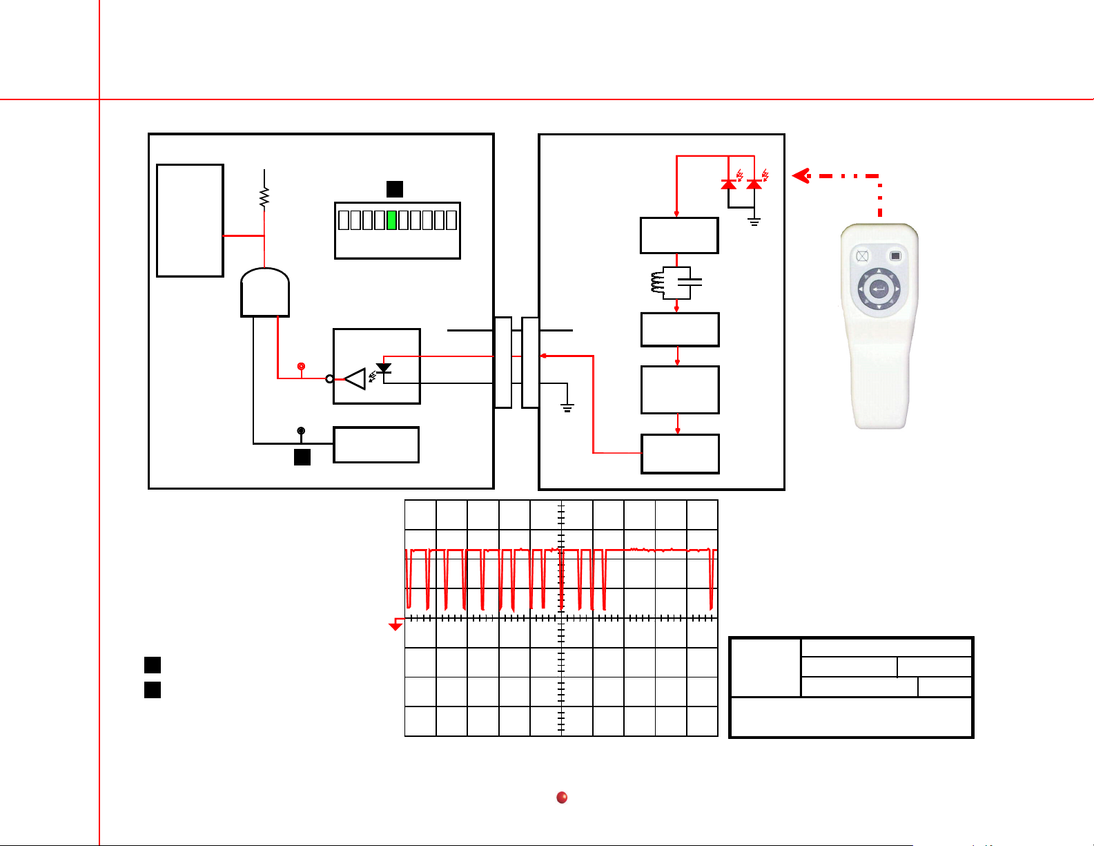
Functional Block 33 – Workstation Control Panel IR Remote / Receiver Interface (5 of 15)
TP5
Contents
9800
Page 5 of 15
11/00
g
GE OEC Training
WSSCOM.DSF
Workstation Control Panel
IR Remote / Receiver Interface
36
Page 37

Functional Block Diagrams Released 11/00
Control Panel Processor PCB
00-876611
U5
80C196KC
CTS
RXD
TXD
RTS
44
17
18
39
DS1 DIAGNOSTIC LED
TP2
TP7
TP6
TP3
E5
E3
1 2
7 8
MAX233
Line Driver
3
20
1
2
U7
4
19
18
5
E2
E4
J2
10
System Interface PCB
00-879054
U26
J1 P1
6 6
8
26 26
6
7 7
25 25
4
P6
1
2
4
3
MAX233
Line Driver
5
18
19
4
Workstation System Interface
Communications Overview 1
2
1
20
3
See
U34
Quad UART
(RS232)
35
CP_CTS
43
CP_RXD
44
CP_TXD
CP_RTS
33
Electronics Box
9800
GE OEC Training
WSSCOM.DSF
1
Segment 7 indicates Serial Data is being received from the System Interface PCB.
Segment 8 indicates Serial Data is being sent to the System Interface PCB.
2
g
Workstation Control Panel
Communication to System Interface
Functional Block 34 – Workstation Control Panel Communication to System Interface (6 of 15)
Contents
Page 6 of 15
11/00
37
Page 38

Functional Block Diagrams Released 11/00
ASSY 00-876613 CONTROL PANEL PROCESSOR
P2
E2 E3
4
E4 E5
U7
1 2
TP2
CTS
3
TP3
RTS
U5
TP6
TXD
TP7
RXD
DS1 DIAGNOSTIC LED
TP7
2 V/div dc
10 ms/div
TP6
2 V/div dc
10 ms/div
1
Segment 7 indicates Serial Data is being received from the System Interface PCB.
Segment 8 indicates Serial Data is being sent to the System Interface PCB.
2
3
TP2 CTS stays at 0 Volts after bootup.
TP3 RTS stays at 0 Volts after bootup.
4
7 8
9800
Page 7 of 15
g
GE OEC Training
WSSCOM.DSF
Workstation Control Panel
Communication Waveforms
11/00
Functional Block 35 – Workstation Control Panel Communication Waveforms (7 of 15)
Contents
38
Page 39

Functional Block Diagrams Released 11/00
System Interface PCB
00-879054
U34
Quad UART
(RS232)
TXD
RXD
TP5
1
TP6
Electronics Box
See
Workstation System Interface
Communications Overview 1
U18
74LS244
Buffer
1
U26
MAX233
Line Driver
P6
Right_RXD
6
Left_RXD
10
Right_TXD
7
Left_TXD
11
R_MON_ON
9
L_MON_ON
13
J1
23
21
4
2
22
1
P1
23
21
4
2
22
1
P2
P2
2
1
6
2
2
1
6
2
RIGHT
MONITOR
LEFT
MONITOR
TP5, TP6
1
Monitor ON = +5 Volts
Monitor failed = 0 Volts
2
P2-6
2
Monitor ON = +11 Volts
Monitor failed = 0 Volts
g
Workstation System Interface
GE OEC Training
WSSCOM.DSF
Monitor Serial Communications
Functional Block 36 – Workstation System Interface Monitor Serial Communications (8 of 15)
Contents
9800
Page 8 of 15
11/00
39
Page 40

Functional Block Diagrams Released 11/00
Back of Monitor
Video
BNC
Connector
P2-2
5 V/div dc
500 us/div
1
P2
P2-1
5 V/div dc
500 us/div
6 5 4
2
Serial communications are present only while adjusting monitor
1
sizing or brightness and contrast adjustments using the RUT utility.
2
P2-6 is +11 volts while monitor is in the ON condition.
3
P2 pins 1 & 2 are at -8 volts in normal operation.
Functional Block 37 – Workstation System Interface Monitor Serial Waveforms (9 of 15)
Contents
3 2 1
3
9800
Page 9 of 15
g
GE OEC Training
WSSCOM.DSF
Workstation System Interface
Monitor Serial Waveforms
11/00
40
Page 41

Functional Block Diagrams Released 11/00
System Interface PCB
00-879054
U34
Quad UART
(RS232)
Workstation System Interface
Communications Overview 1
TXDA
RXDA
20
19
See
Line Driver
1
20
U23
MAX233
18
19
P6
14
15
16
Electronics Box
J1 P1
28 28
10 10
29 29
TS_RXD
TS_TXD
TS_RTN
P1
2
5
Right Monitor
Touch Screen
3
1
9800
GE OEC Training
WSSCOM.DSF
Internal operation of the Touch Screen is
1
propriety and not supplied by the vendor.
g
Workstation Touch Screen to
System Interface Communications
Functional Block 38 – Workstation Touch Screen to System Interface Communication (10 of 15)
Contents
Page 10 of 15
11/00
41
Page 42
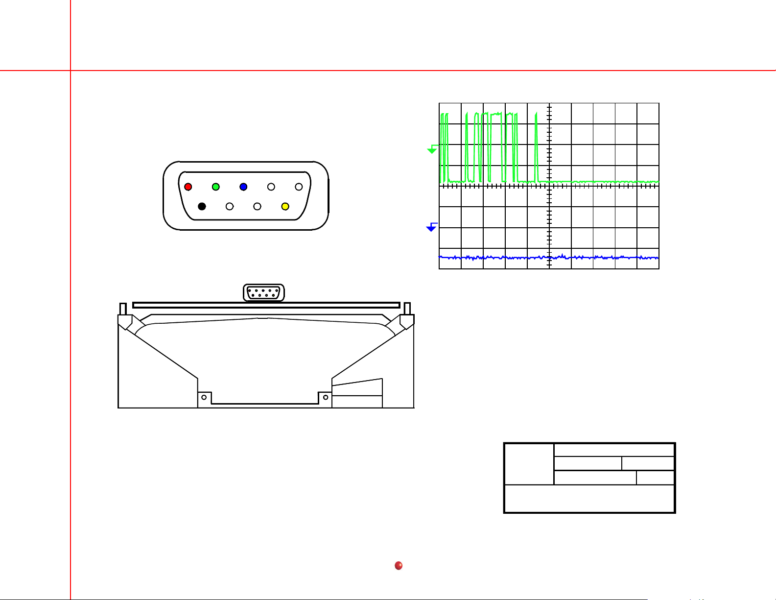
Functional Block Diagrams Released 11/00
1 Red +15Volts
2 Green TS_TXD
3 Blue TS_RXD
5 White TS_RTN
6 Black Ground
9 Yellow +12 Volts
1 2 3 4 5
6 7 8 9
P1
1 2 3 4 5
6 7 8 9
P1-2
5 V/div dc
1 ms/div
P1-3
5 V/div dc
1 ms/div
Monitor
Rear View
9800
Page 11 of 15
g
GE OEC Training
WSSCOM.DSF
Workstation Touch Screen to
System Interface Waveforms
Functional Block 39 – Workstation Touch Screen to System Interface Waveforms (11 of 15)
Contents
11/00
42
Page 43

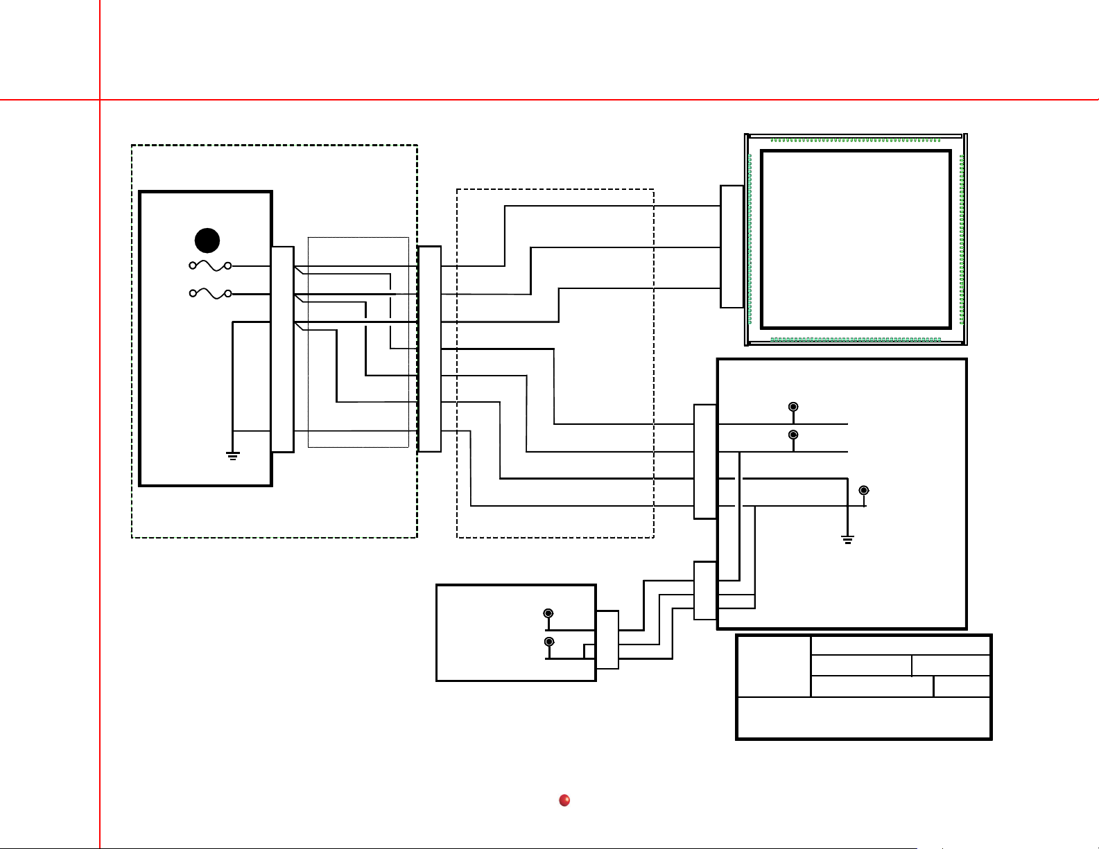
Functional Block Diagrams Released 11/00
System Interface PCB
00-876611
P11
DIAG_RXD
1
DIAG_TXD
14C
20
19
00-879471
Electronics Box
See Arcnet Communications Functional Diagram Page 1 of 2
1
External Interface
00-879184
P1
20
19
P4
7
6
RUT Diagnostic Cable
Laptop
GE OEC Training
g
WSSCOM.DSF
Workstation
Remote Diagnostics Interface
Functional Block 40 – Workstation Remote Diagnostic Interface (12 of 15)
Contents
9800
Page 12 of 15
11/00
43
Page 44

Functional Block Diagrams Released 11/00
U34
Quad UART
(RS232)
CE
A
U25
MAX233
U26
MAX233
U18 U24
74LS244 MAX233
U23
Max233
Host Buffered Data Bus
U56
Data Buffer
Spare
To Control Panel
see page 6 of 15
To LMON & RMON
see page 8 of 15
To Touch Screen
see page 10 of 15
1
U58
Option Prom
See Arcnet Communications
Functional Diagram
U7
RS485
Transceiver
Sel 0
Sel 1 U21 Ext. Relays
U37
Pentium Arcnet
Controller
Host Buffered Address Bus
2
CS
OE
U59
Address Buffer
CS
U57
I/O Map
Decoder
Sel 2 U28 Ext. Relays
Sel 3 U38 Ext. Relays
Sel 4 U27 PCB Rev.ID
Sel 5 U35 Config. Switch
Sel 6 U22 DS1 Diagnostics
Sel 7 U14 DS2 Diagnostics
Sel 8 U42 Voltage Sense
Sel 9 U45 Temp Sense &
Amb. Light Sense
Sel 10 U44 Temp Sense &
Voltage Sense
Sel 11 U30 VCR Control
Sel 12 U29 VCR Control
Sel 13 U4 Hex Diag. Display
Sel 14 U34 Quad UART
Sel 15
B_RESET
14A
A
System Interface PCB
00-879054
See System Interface I/O Map Select Lines Diagram
1
Pages 2 of 10, 4 of 10, 6 of 10, 7 of 10, 8 of 10, 9 of 10
2
Option Prom U58 prevents access to DOS with a non OEC boot disk.
Host Data Bus
ISA Slot 2
Host Pentium CPU
Host Address Bus
GE OEC Training
g
WSSCOM.DSF
Workstation System Interface
Communications Overview 1
Functional Block 41 – Workstation System Interface Communications Overview 1 (13 of 15)
Contents
9800
Page 13 of 15
11/00
44
Page 45

Functional Block Diagrams Released 11/00
13A
U43
MCHC16Z1
Diagnostic
Processor
MOD_TXD
MOD_RXD
1
B_RESET*
TP15
WD_STRB
2
TP25
RESET*
TP19
16MHZ_CLK
U53 - U55
74HC244
Address
Buffer
U40, U49
74HTC245
Data
Buffer
Modem Control Lines
U32
74LS244
Buffer
U33
MAX1232
Power Monitor
Watchdog Timer
3
Y1
Diagnostic Address Bus
Diagnostic Data Bus
VCC
U52
Address
Decoder
U46
MAX239
Line Driver
RESET*
U36
Remote
Diagnostics
ARCNET
Controller
U51, U50
AM29F010
Flash EPROM
Program / Boot
Prom
U48, U47
SRAM
U20
RS485
Transceiver
See Arcnet
Communications
Functional Diagram
P12
1 MD_DCD
2 MD_RXD
3 MD_TXD
4 MD_DTR
5 GROUND
6 MD_DSR
7 MD_RTS
8 MD_CTS
9 MD_RI
TP2
ARCNET_HI
TP8
ARCNET_LO
15B
U16
System Interface PCB
MAX233
Line Driver
00-879054
B_RESET is controlled by the Host Pentium Processor.
1
2
WD_STRB resets the Watchdog timer as the Diagnostic Processor runs.
RESET* at TP25 is normally High. Diagnostic Processor U43 will be reset if VCC drops below 4.65 Volts,
3
WD_STRB signal is lost, or if the Host Pentium Processor issues a reset via B_RESET at TP15.
P11
19 DIAG_TXD
20 DIAG_RXD
21 DIAG_RTN
GE OEC Training
g
WSSCOM.DSF
Workstation System Interface
Communications Overview 2
Functional Block 42 – Workstation System Interface Communications Overview 2 (14 of 15)
Contents
12C
9800
Page 14 of 15
11/00
45
Page 46
Functional Block Diagrams Released 11/00
MD_DCD
MD_RXD
14B
MD_TXD
MD_DTR
GROUND
MD_DSR
MD_RTS
MD_CTS
MD_RI
System Interface PCB
00-879054
Electronics Box
00-879475
P12
1
2
3
4
5
6
7
8
9
P2
J2
1
1
2
2
3
3
4
4
5
5
6
6
7
7
8
8
9
9
00-880651
1
MD_DCD
2
MD_RXD
3
MD_TXD
4
MD_DTR
5
GROUND
6
MD_DSR
7
MD_RTS
8
MD_CTS
9
External Modem
00-880811
MD_RI
1
00-880648
1
2
3
4
RJ11
Connector
1
Analog
2
Telephone
3
4
To
Jack
Workstation
Rear Panel
1
Not currently installed.
Functional Block 43 – Workstation Modem to System Interface Communications (15 of 15)
Contents
9800
Page 15 of 15
11/00
g
GE OEC Training
WSSCOM.DSF
Workstation Modem to
System Interface Communications
46
Page 47
Functional Block Diagrams Released 11/00
SYSTEM INTERFACE PCB
00-879054
U37 Host Arcnet Controller
Sel 0
10P
HOST PENTIUM CPU
ISA SLOT 2
Host Pentium Address Bus
U57
Address
Decoder
1
Sel 1
U21 Ext. Relays
U28 Ext. Relays
Sel 2
U38 Ext. Relays
Sel 3
U27 PCB Rev.ID
Sel 4
U35 Config. Switch
Sel 5
Sel 6
U22 DS1 Diagnostics
U14 DS2 Diagnostics
Sel 7
U42 Voltage Sense
Sel 8
U45 Temp Sense & Amb. Light Sense
Sel 9
U44 Temp Sense & Voltage Sense
Sel 10
U30 VCR Control
Sel 11
Sel 12
U29 VCR Control
Sel 13
U4 Hex Diagnostic Display
U34 Quad UART
Sel 14
Sel 15
U58 Option Prom
2A
2B
2C
4D
4E
7H
8K
8L
10N
10O
6F
6G
7I
7J
9M
1
See Workstation System Interface Communications Overview1 Page 13 of 15
Functional Block 44 – System Interface I/O Map Select Lines (1 of 10)
Contents
GE OEC Training
g
SIIOSELC.DSF
System Interface I/O
Map Select Lines
9800
Page 1 of 10
11/00
47
Page 48

Functional Block Diagrams Released 11/00
1A
1B
1C
SEL 1
C1
EN
U21
LATCH
SEL 2
C1
EN
U28
LATCH
SEL 3
EN2
EN1
U38
LATCH
Host Buffered Data Bus
12
13
14
12
13
14
15
16
17
18
19
SYSTEM INTERFACE PCB
9
U17
10
4
U17
5
1
U17
2
8
5
4
2
11
13
15
17
See Workstation System Interface
Communications Overview1
8
6
3
Page 13 of 15
00-879054
1
U19
INVERTING
2
LATCH
3
4
5
6
7
8
PWR_INJCT
18
SPARE1
17
SPARE2
16
X-RAY_ON
15
RM_IN_USE
14
SPARE3
13
ISOLAT_RLY_CNTL
11
RELAY_+12V
10
RELAY_GND
9
X-RAY_LMP_RTN
12
RELAY_GND
RELAY_GND
+12V
P11
7
8
26
2
1
P6
19
P5
21
24
3
4
5
6
3A
3B
3C
GE OEC Training
g
SIIOSELC.DSF
System Interface I/O
External Relay Control 1
Functional Block 45 – System Interface I/O External Relay Control 1 (2 of 10)
Contents
9800
Page 2 of 10
11/00
48
Page 49
Functional Block Diagrams Released 11/00
P4
SYSTEM INTERFACE 00-879054
1
2
P11
3
6
7
2A
26
2
1
P2
1
2
P1
3
6
7
26
2
1
ARCNET_HI_2
ARCNET_LO_2
A
TP2
+12V
K1
+12V
13
11
9
6
8
K3
4
1
-
16
11
6
8
R1
+12V
A
9
+12V
A
13
K2
4
1
-
16
K4
13
4
1
16
-
13
4
+12V
A
1
-
16
A
ARCNET_HI_2
ARCNET_LO_2
11
9
6
8
PWR_INJCT_1
PWR_INJCT_2
X-RAY_ON_1
X-RAY_ON_2
RM_IN_USE_1
RM_IN_USE_2
11
9
6
8
EXTERNAL
INTERFACE PCB
P4
P3
1
2
2
1
6
2
1
7
3
8
00-879184
2B
+5V
2C
DS2
X-RAY ON
9
LAMP
ELECTRONICS BOX
DC DISTRIBUTION
PCB
00-879119
Room Interface
1
External Arcnet
2
GE OEC Training
g
SIIOSELC.DSF
System Interface I/O
External Relay Control 2
P5
21
24
P6
19
18
P1
27
P5
21
24
Functional Block 46 – System Interface I/O External Relay Control 2 (3 of 10)
Contents
ELECTRONICS
BOX
9800
Page 3 of 10
11/00
49
Page 50

Functional Block Diagrams Released 11/00
+5
VCC
R65
10K
R48 75
R46 75
R44 75
R42 75
R49 75
R47 75
R45 75
R43 75
ASSEMBLY
I.D. RESISTORS
U15
45
3
2
1
CONFIGURATION
SWITCHES
1
1
6
7
8
2
5A
SYSTEM INTERFACE PCB
00-879054
B_CONFIG_3
B_CONFIG_2
B_CONFIG_1
B_CONFIG_0
See Workstation System Interface
Communications Overview1
Page 13 of 15
R5
10K
11
13
Host Buffered Data Bus
SEL 4
1
19
8
6
4
2
11
13
15
17
SEL 5
1
19
8
6
4
2
15
17
EN
EN
EN
EN
1D
2
1
U27
LATCH
1E
2
1
U35
LATCH
12
14
16
18
9
7
5
3
12
14
16
18
9
7
5
3
1
Installed resistors indicate PCB revision level.
2
All switches must be set to the OFF or OPEN position.
Functional Block 47 – System Interface I/O Configuration Switch and ID (4 of 10)
Contents
GE OEC Training
g
SIIOSELC.DSF
System Interface I/O
Config Switch & ID
9800
Page 4 of 10
11/00
50
Page 51

Functional Block Diagrams Released 11/00
1
CONFIG_3
CONFIG_2
CONFIG_1
CONFIG_0
B
I
C
P
A
L
B
A
L
N
E
E
P4
12
11
10
9
ELECTRONICS
BOX
R9 10K
R8 10K
R7 10K
R6 10K
R21KR31KR41KR5
1K
+5V
VCC
EXTERNAL INTERFACE
00-879184
P1
25
24
23
22
P11
25
24
23
22
13
11
9
5
SYSTEM INTERFACE
00-879054
U39
Inverting
Latch
4A
4
5
MCHC16Z1
Diagnostic
6
Processor
7
U43
1
External Arcnet
GE OEC Training
g
System Intrface I/O
External Cable ID
Functional Block 48 – System Interface I/O External Cable ID (5 of 10)
Contents
9800
SIIOSELC.DSF
Page 5 of 10
11/00
51
Page 52
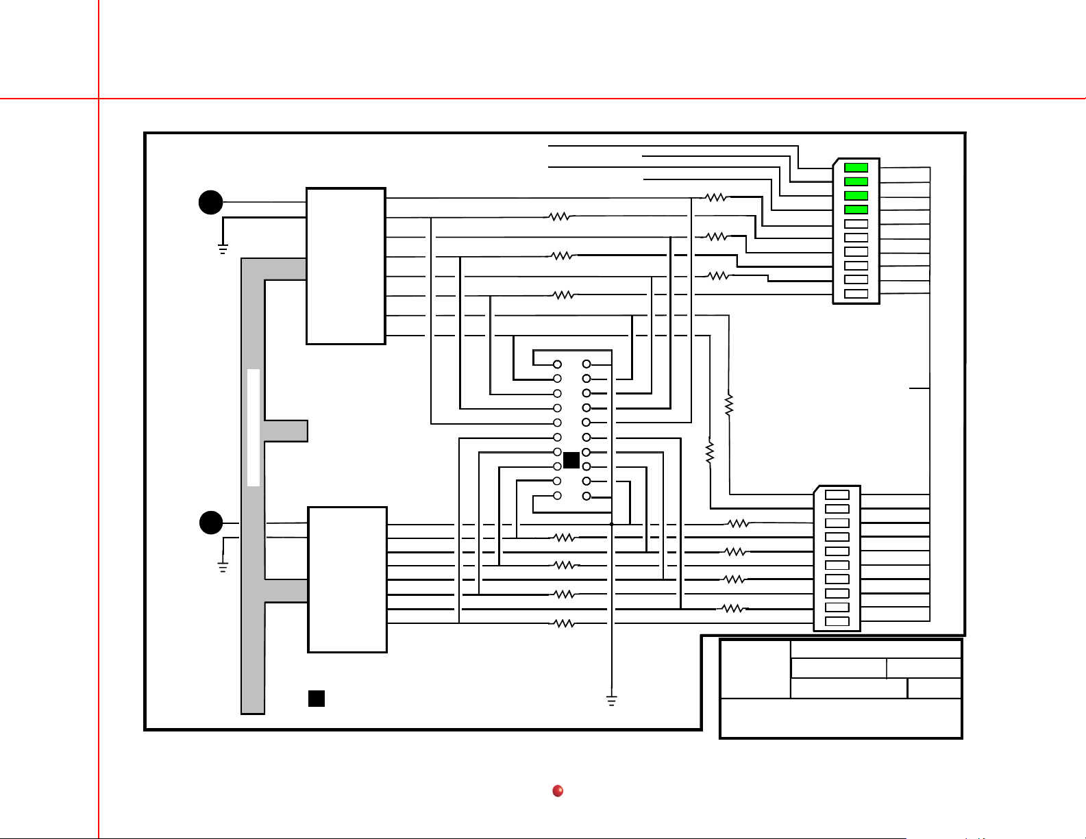
Functional Block Diagrams Released 11/00
SYSTEM INTERFACE
00-879054
SEL 6
1F
Host Buffered Data Bus
1G
C1
EN
Workstation System Interface
SEL 7
C1
EN
12
13
14
U22
LATCH
Communications Overview1
15
16
17
18
19
See
Page 13 of 15
U14
LATCH
PWR_OK
OPT_PROM_EN
INTERCON_OK
FRAME_SYNC_OK
1
34
5
7
910
11
13
15
17
19
2
6
8
E
12
1
14
1
16
18
20
15
16
17
18
19
20
DS1
10
9
8
7
6
5
4
3
2
1
+5V
VCC
DS2
10
9
8
7
6
5
4
3
2
1
GE OEC Training
1
Function not implemented.
g
SIIOSELC.DSF
System Interface I/O
DS1, DS2 Diagnostic LEDs
Functional Block 49 – System Interface I/O DS1, DS2 Diagnostic LEDs (6 of 10)
Contents
9800
Page 6 of 10
11/00
52
Page 53

Functional Block Diagrams Released 11/00
CINE_+5V_SEN
CINE_+3.3V_SEN
VIDCNT_+5V_SEN
VIDCNT_+3.3V_SEN
1
DSPCNT_+5V_SEN
DISPCNT_+3.3V_SEN
1
IP_+V5_SEN
IP_+3.3V_SEN
PCIDA_+5V_SEN
CPP_+5V_SEN
CPP_+12V_SEN
PCIDA_+12V_SEN
SPARE_+12V_SEN
SPARE_+12V_SEN
TEMP_SEN_1+
TEMP_SEN_1-
TEMP_SEN_2_+
1
TEMP_SEN_2_-
X-RAY_LMP
1
AMB_LIGHT_2
AMB_LIGHT_1
1
P5
2
3
4
5
6
7
8
9
10
11
12
13
14
16
17
18
19
20
18
21
20
P6
D
VCC
-12V
-12V
D
-12VMB
U12
U12
D
U11
D
SYSTEM INTERFACE 00-879054
See Workstation DC Distribution Page 8 of 17
-12V
D
R27
U11
SEL 8
1H
U42
A/D
CONVERTER
SEL 10
1J
U44
A/D
CONVERTER
D
SEL 9
1I
+12VMB
VCC
+12V
+5VMB
U45
A/D
CONVERTER
CLK 3.5854 MHZ
+5VREF
CLK 3.5854 MHZ
+5VREF
CLK 3.5854 MHZ
+5VREF
Host Buffered Data Bus
9800
Page 7 of 10
11/00
g
GE OEC Training
SIIOSELC.DSF
System Interface I/O
A/D Sense
Functional Block 50 – System Interface I/O A/D Sense (7 of 10)
Contents
53
Page 54

Functional Block Diagrams Released 11/00
SELECT 11
C1
EN
D
SELECT 12
EN
EN
Host Buffered Data Bus
1K
U30
LATCH
1L
U29
LATCH
VCC
U9
BUFFER
U8
VCC
BUFFER
See Workstation System Interface
Communications Overview1
Page 13 of 15
R7
REWIND*
FFORWARD*
PLAY*
PAUSE*
RECORD*
SPARE*
STOP*
SPARE*
SHIELD
VCC
U17
D
FFORWARD_IN
REWIND_IN
PAUSE_IN
RECORD_IN
PLAY_IN
SYSTEM INTERFACE 00-879054
P12
J2
ELECTRONIC
BOX
P2
TO/FROM
VCR
SONY
EJECT REC
STOP REW PLAY
S VHS HI-FI
F FWD
PAUSE
POWER
g
System Interface I/O
Functional Block 51 – System Interface I/O VCR Control (8 of 10)
Contents
9800
GE OEC Training
SIIOSELC.DSF
VCR Control
Page 8 of 10
11/00
54
Page 55

Functional Block Diagrams Released 11/00
SELECT 13
1M
Host Buffered Data Bus
1
Diagnostic Data Bus
SYSTEM INTERFACE
00-879054
See Workstation System Interface Communications Overview 1 page 13 of 15
1
2
See Workstation System Interface Communications Overview 2 page 14 of 15
00 code is displayed on U2, U1 during normal operation.
3
2
U4
LATCH
U31
LATCH
3
U2
3
D
U1
g
9800
GE OEC Training
SIIOSELC.DSF
Page 9 of 10
11/00
System Interface I/O
U1, U2 Diagnostic Display
Functional Block 52 – System Interface I/O U1, U2 Diagnostic Display (9 of 10)
Contents
55
Page 56
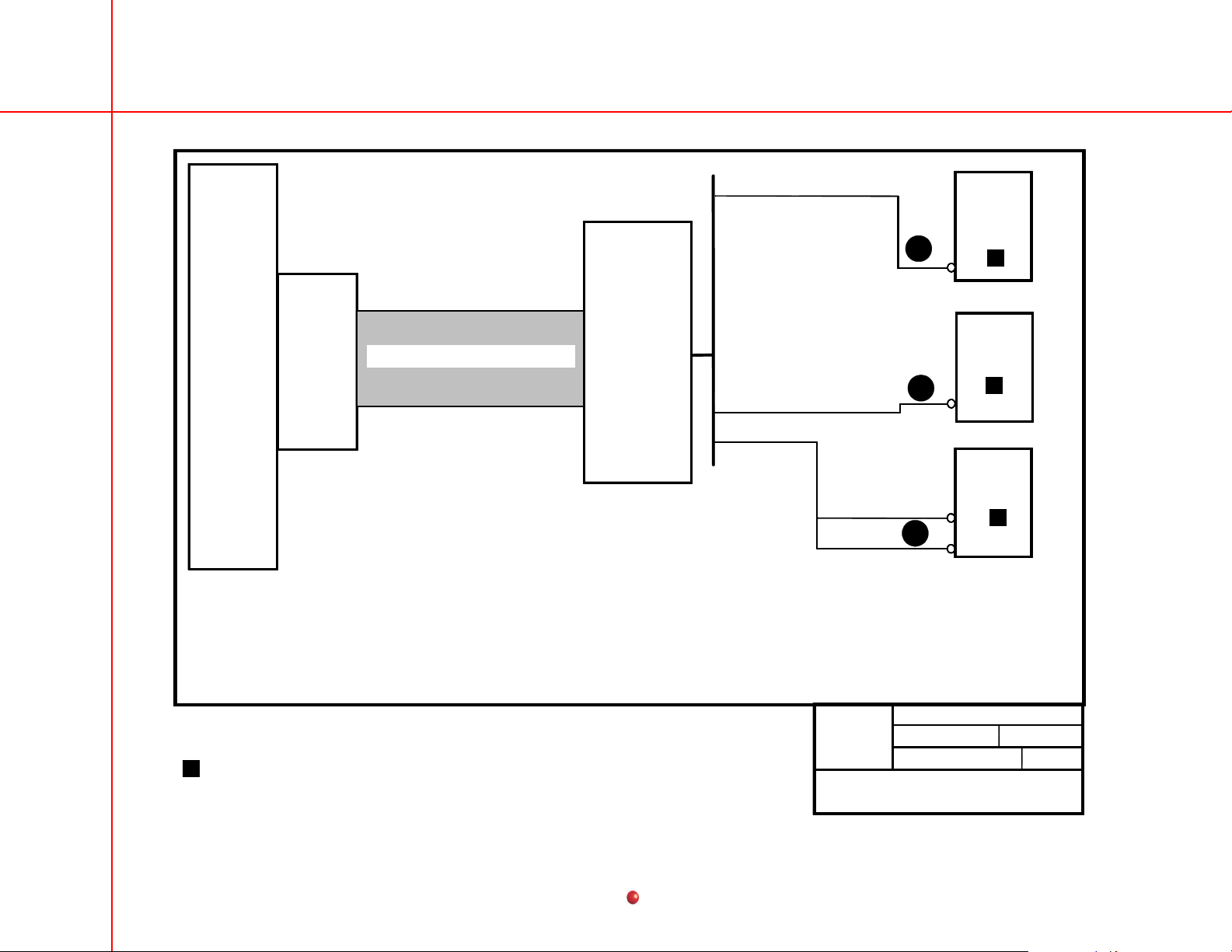
Functional Block Diagrams Released 11/00
HOST PENTIUM CPU
ISA SLOT 2
SYSTEM INTERFACE PCB
00-879054
Host Pentium Address Bus
U57
Address
Decoder
Sel 0
Sel 14
Sel 15
1P
3
1O
1N
U37
Host
Arcnet
Contrlr
CS
U34
Quad
UART
CS
U58
Option
Prom
CS
OE
1
1
1
1
1
1
GE OEC Training
See Workstation System Interface Communications Overview 1 page 13 of 15
1
g
SIIOSELC.DSF
System Interface I/O
Arcnet, Quad UART, Opt PROM
Functional Block 53 – System Interface I/O ARCNET, Quad UART, Option PROM (10 of 10)
Contents
9800
Page 10 of 10
11/00
56
Page 57

Functional Block Diagrams Released 11/00
Image Path
Overview
Page 2
Image Path into
Video Controller PCB
Page 3 Page 4 Page 5
Image Path out of
Video Controller PCB
Image Path
Waveforms
Page 7
Image Path in
Display Adapter PCB
Functional Block 54 – Image Path (1 of 7)
Image Path in
Display Controller PCB
Page 6
9800
GE OEC Training
g
Functional Diagram Map
IMAGEP.DSF
Image Path
Page 1 of 7
11/00
Contents
57
Page 58
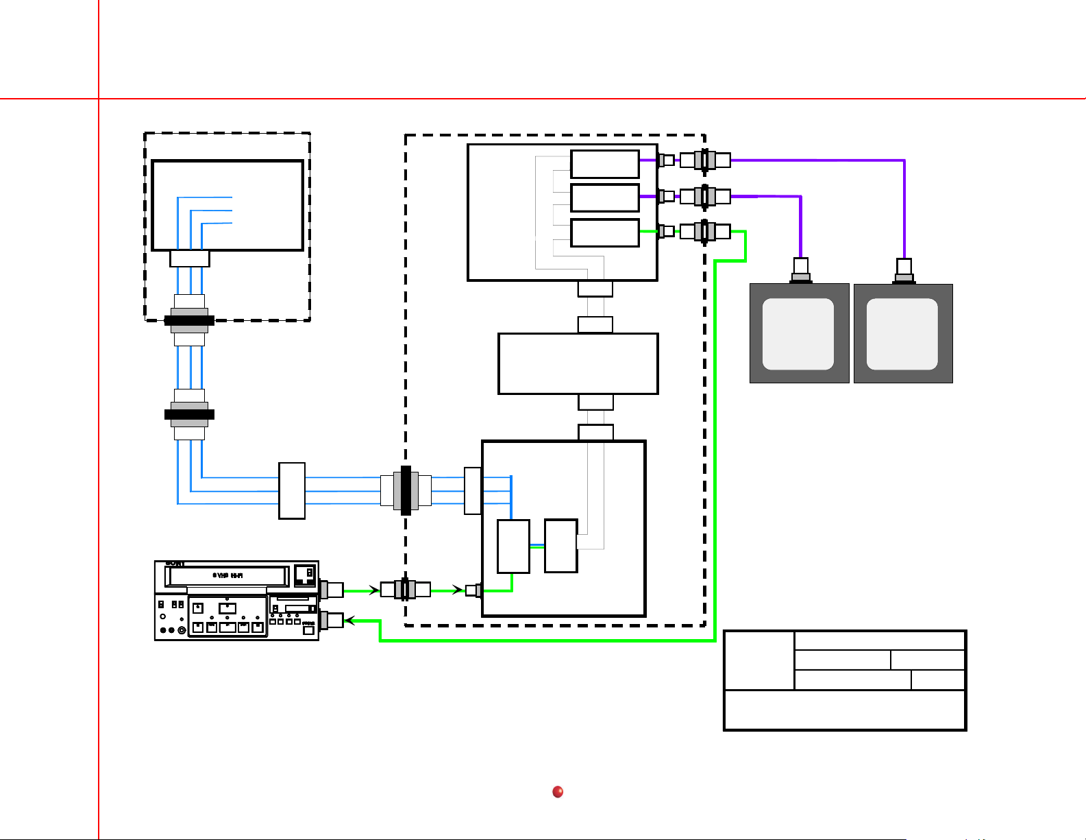
Functional Block Diagrams Released 11/00
Camera Cover Assy.
CCD Camera Assy.
Video_Hi
Video_Lo
Video_Shld
P2 8 4 3
J7
High Voltage &
Control Cable Assy.
J3
Lemo Receptacle
Cable Assy.
Interconnect
J1
Cable Assy.
13
2
1
Interconnect
Plug
Video
Output
J3
J6
EMI Box
Controller
P6
8
4
3
J5
Display
Adapter
or
Display
Image
Processor
Mux
A/D
Right DAC
P9
P5
P4
P3
U9
U4
Left DAC
U40,U32
Left DAC
P8
P5
P12
P7
P8
P5
P3 P3
LEFT
MONITOR
RIGHT
MONITOR
EJECT REC
STOP REW PLAY
F FWD PAUSE
VCR
Video Controller PCB
Video
Input
Functional Block 55 – Image Path Overview (2 of 7)
Contents
g
9800
GE OEC Training
IMAGEP.DSF
Image Path
Overview
Page 2 of 7
11/00
58
Page 59

Functional Block Diagrams Released 11/00
Video Controller PCB
TP1
7A
+
U8
MAX452
-
U5
MAX452
+
U14
MUX
IN0
+
IN1
-
IN2
IN3
A0 A1
U16
GS4881
Sync Stripper
U23
DG411
BP
TP31
MUXVID
U22
HFA1103
X2 Video
Separator
U17
MAX9698
Hi Res
Sync Stripper
U6
GS4581
VCR
Sync Stripper
ISA Address Decoder
TP48
VID
TP18
COMP_SYNC
TP16
VCR_HSYNC
U65
U18
SYNCGEN1
FPGA
TP11
BP_CLAMP*
TP8
HSYNC*
2
TP7
VSYNC*
VIDSEL0
TP2
Pilot Tone
4A
4B
4C
4D
4E
1
Video_Lo
Video_Hi
Video_Shld
7C
VCR
Video
P5
P6
4
TP15
8
3
See Pilot Tone Functional Diagram page 1 of 1.
1
See Frame Sync Functional Diagram page 1 of 2.
2
Functional Block 56 – Image Path Info Video Controller PCB (3 of 7)
Contents
ISA D0 - D7
ISA Slot 1
Host Pentium CPU
GE OEC Training
g
IMAGEP.DSF
Image Path into
Video Controller PCB
9800
Page 3 of 7
11/00
59
Page 60
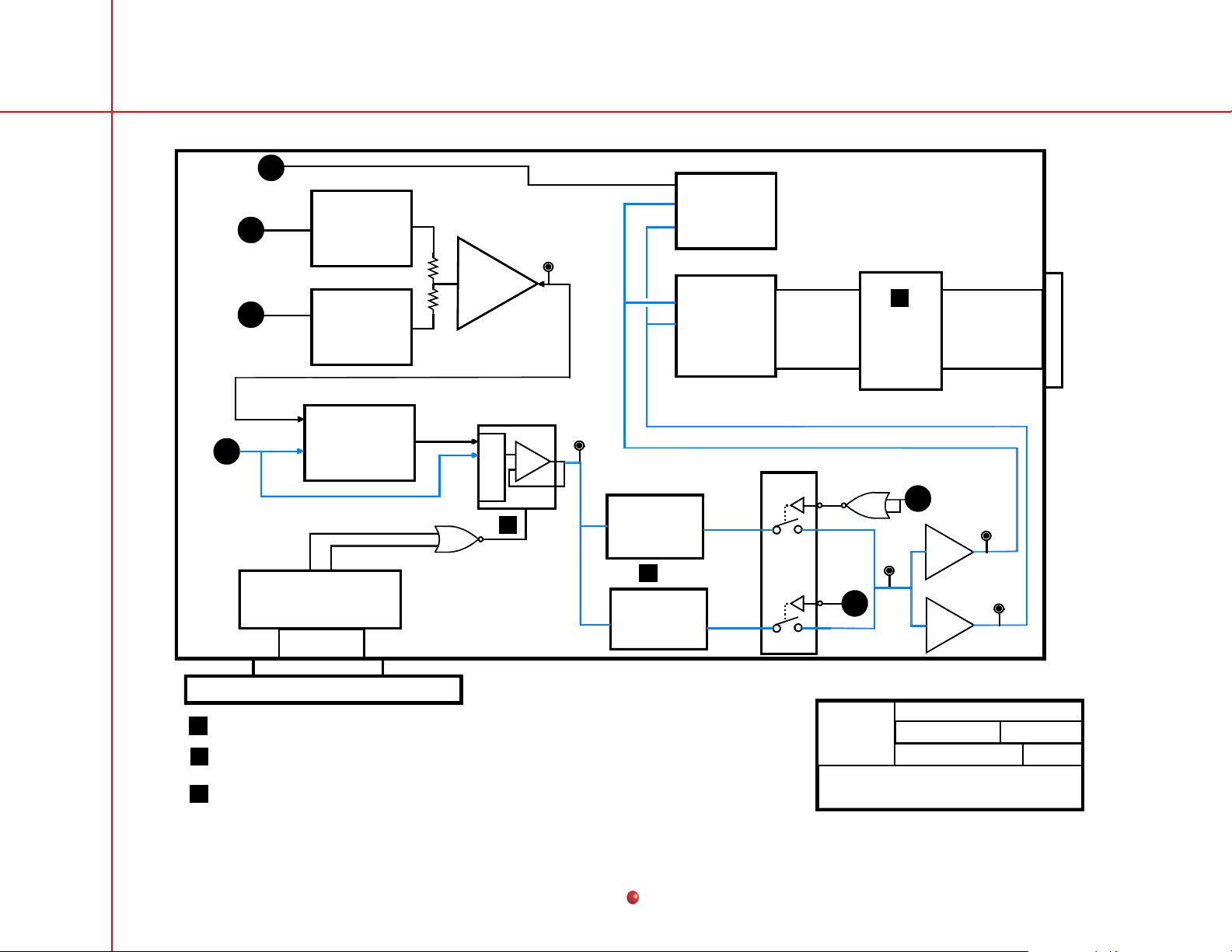
Functional Block Diagrams Released 11/00
BP_CLAMP*
HSYNC*
VSYNC*
VID
3B
3C
3D
3A
ISA Address Decoder
Horizontal
Anti-Vignetting
Circuit
U23, U60, U54
Vertical
Anti-Vignetting
Circuit
U23, 60, U55
Voltage Controlled
Gain Amplifier
U32
Uncorrected Video
U65
ISA D0 - D7
ISA Slot 1
MAGSEL0
MAGSEL1
Summing
Shading
Corrected
Video
U24
Amplifier
U57
IN0
IN1
IN2
IN3
Host Pentium CPU
Interpolates value of low scan VCR video to high scan format.
1
Shading corrected video is applied in Normal image tube field size.
2
Uncorrected video is applied in Mag 1, Mag 2 image tube field size.
25 mHz filter is used when aquiring video during X-Rays.
3
5 mHz filter is used when reviewing video from a VCR.
DC Restoration
Clamp Circuits
VCR
3
U34, U59, U43
A/D Converter
AD5800
U42
AD_IN0
to
AD_IN11
U34
DG411
TP47
AVIG
TP43
U33
+
-
A0
2
Anti Alias Filter
5 MHZ LP
Hi Res Video
Anti Alias Filter
25 MHZ LP
Video Controller PCB
1
Pixel
Interpolator
U46
TP50
3E
-
U41
MAX452
U24
3E
+
MAX452
P3
To Image Processor
VC_D0
to
VC_D11
TP51
TP52
U56
9800
Page 4 of 7
11/00
g
GE OEC Training
IMAGEP.DSF
Image Path out of
Video Controller PCB
Functional Block 57 – Image Path out of Video Controller PCB (4 of 7)
Contents
60
Page 61
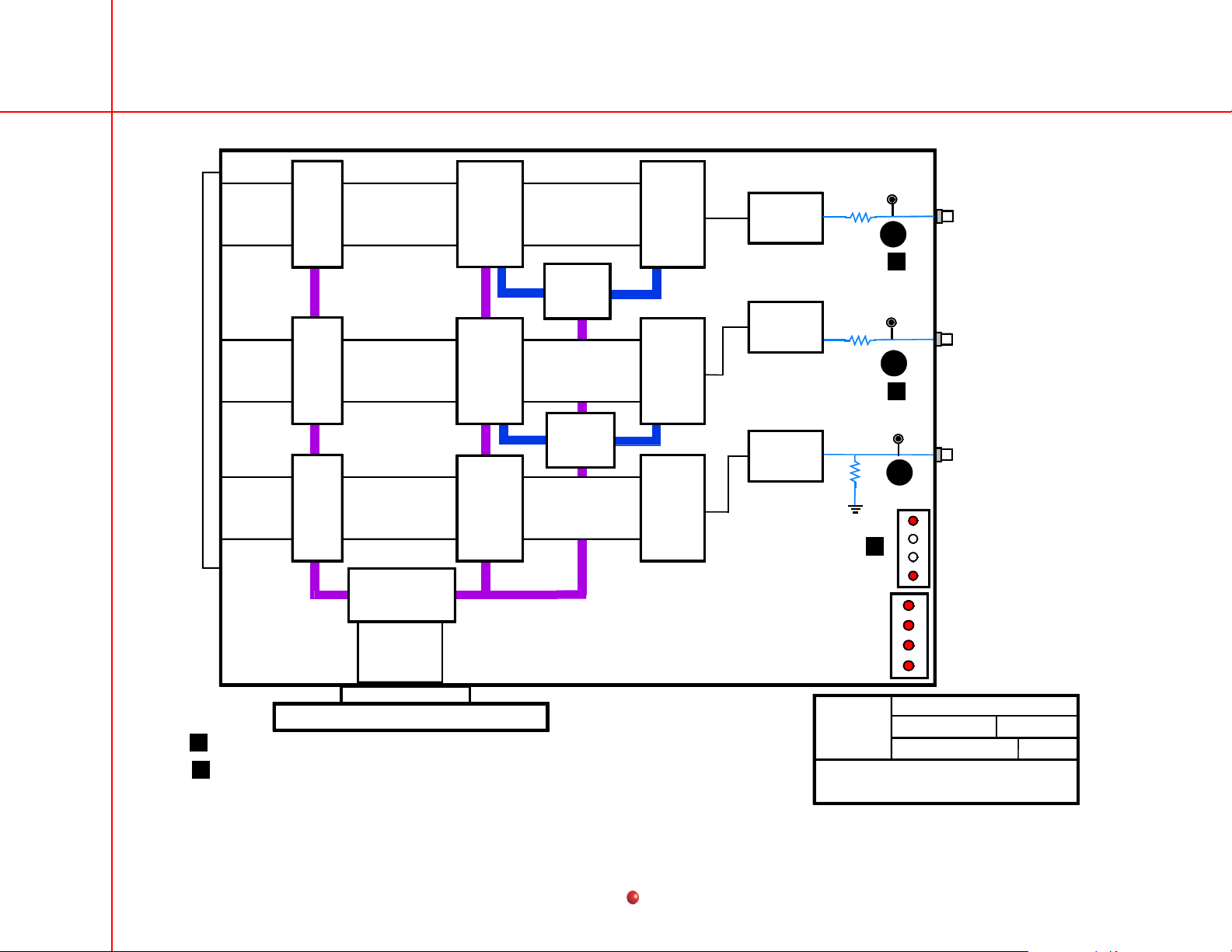
Functional Block Diagrams Released 11/00
P9
LD_D0
to
LD_D7
RD_D0
to
RD_D7
From Image Processor
AD_D0
to
AD_D7
U12
Latch
U16
Latch
U17
Latch
Left_Pix_Data 0
to
Left_Pix_Data 7
RT_Pix_Data 0
to
RT_Pix_Data 7
AUX_Pix_Data 0
to
AUX_Pix_Data 7
U43
PCI BUS
INTERFACE
PCI BUS 0
Left
Frame
Buffer
U26, U21,
U22, U23,
U24
Right
Frame
Buffer
U31, U27,
U28, U29,
U30
TV_Video
Control
U40
L_Display_Data
U36
Left Video
Control
R_Display_Data
U37
Right Video
Control
DAC_VID DATA
RAMDAC3
TVP3030
U4
RAMDAC4
TVP3030
U9
BT121
DAC
U32
Display Adapter PCB
Video Buffer
MAX499
U5
Video Buffer
MAX499
U7
Video Buffer
MAX499
U6
Left Monitor
Video TP10
7B
75
1
Right Monitor
Video TP15
75
7B
1
VCR Input
Video TP11
75
7C
2
DS2
P12
DS1
P5
Fast Scan Video
to Left Monitor
P8
Fast Scan Video
to Right Monitor
Interlaced Video
to VCR
Conf_Done
RFPGA_LED
LFPGA_LED
PLX_CS0
+2.5V
+3.3V
+5V
-5V
PCI Slot 5
Host Pentium CPU
The Display Adapter PCB produces a 75 hZ display rate.
1
Conf_Done and PLX_CS0 LED's on DS1 lit during normal operation.
2
RFPGA_LED and LFPGA_LED blink occassionaly during normal operation.
Functional Block 58 – Image Path in Display Adapter PCB (5 of 7)
Contents
GE OEC Training
g
IMAGEP.DSF
Image Path in
Display Adapter PCB
9800
Page 5 of 7
11/00
61
Page 62

Functional Block Diagrams Released 11/00
P9
LD_D0
to
LD_D7
RD_D0
to
RD_D7
From Image Processor
AD_D0
to
AD_D7
U12
Latch
U16
Latch
U17
Latch
Left_Pix_Data 0
to
Left_Pix_Data 7
RT_Pix_Data 0
to
RT_Pix_Data 7
AUX_Pix_Data 0
to
AUX_Pix_Data 7
U43
PCI BUS
INTERFACE
PCI BUS 0
Left
Frame
Buffer
U26, U21,
U22, U23,
U24
Right
Frame
Buffer
U31, U27,
U28, U29,
U30
TV_Video
Control
U40
L_Display_Data
U36
Left Video
Control
R_Display_Data
U37
Right Video
Control
DAC_VID DATA
RAMDAC3
TVP3030
U4
RAMDAC4
TVP3030
U9
BT121
DAC
U32
Display Controller PCB
Video Buffer
MAX499
U5
Video Buffer
MAX499
U7
Video Buffer
MAX499
U6
Left Channel
Conf_Status
Indicators
Right Channel
Conf_Status
Indicators
Left Monitor
Video TP1
75
Right Monitor
Video TP13
75
75
DS1
1
DS2
P5
Fast Scan Video
to Left Monitor
P8
Fast Scan Video
to Right Monitor
P12
Interlaced Video
to VCR
7C
PLX LOAD OK
UNBLANK
IP
VIDEO
ALTERA LOAD OK
UNBLANK
IP
VIDEO
PCI Slot 5
Host Pentium CPU
The following LED's are normally on indicating proper operation of the control cirucuits:
1
PLX_LOAD OK< ALTERA LOAD OK, VIDEO.
The UNBLANK and IP LED's blink during normal operation.
Functional Block 59 – Image Path in Display Controller PCB (6 of 7)
Contents
GE OEC Training
g
IMAGEP.DSF
Image Path in
Display Controller PCB
9800
Page 6 of 7
11/00
62
Page 63
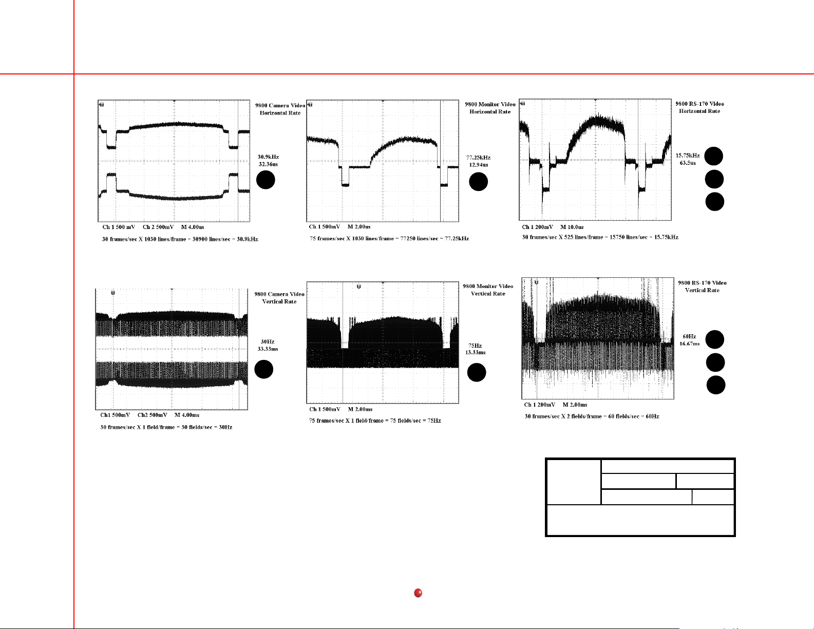
Functional Block Diagrams Released 11/00
3C
3A
3A
5B
5B
g
9800
GE OEC Training
IMAGEP.DSF
Image Path
Waveforms
5C
6C
3C
5C
6C
Page 7 of 7
11/00
Functional Block 60 – Image Path Waveforms (7 of 7)
Contents
63
Page 64

Functional Block Diagrams Released 11/00
J3
EMI Box
Image
Processor
Video Controller PCB
Pixel Clock
Horizontal Sync
Vertical Sync
Field Index
Generator
P6
6
5
1
T1
Camera Cover Assy.
CCD Camera Assy.
Pilot_Hi
Pilot_Lo
Pilot_Shld
P2 1 5 6
J6
High Voltage &
Control Cable Assy.
J3
Interconnect
Plug
J1
16
5
4
Lemo Receptacle
Cable Assy.
TP6 is high (4.5 V) when Pilot Tone is detected.
1
TP6 is low ( .5 V) when Pilot Tone is not detected.
If no Tone is detected Y1 provides the timing signal.
See Image Path into Video Controller PCB Functional Diagram page 3 of 7.
2
Interconnect
Cable Assy.
U18
Sync
U1
Diff.
Amp
TP2
Pilot
Tone
P4
P3
TP19
2
U2
74LS123
Tone
Detect
Y1
39 mHz
TP6
Pilot
Detect
1
TP2
1 V/div dc
10 ns/div
9800
Page 1 of 1
11/00
g
GE OEC Training
PTONE.DSF
Pilot Tone Functional Diagram
Functional Block 61 – Pilot Tone (1 of 1)
Contents
64
Page 65

Functional Block Diagrams Released 11/00
CCD
Camera
X-ray Controller
U21
486
Embedded
Processor
1
2
IRQ1
P6
P7
TP24
Video
Pilot Tone
INT_SYNC*
P1
20
21
Backplane
P2
3
8
P1 Interconnect Plug
10
11
P6
P3
9
10
Image Processor
Video Controller
3
Generator
2
System Interface
Frame Sync
U18
Sync
P4
P3
P8
P10
DS1
TP7
V_SYNC*
Frame
Sync
OK
4
Backplane
See Image Path Overview Functional Diagram page 2 of 7.
1
See Pilot Tone Functional Diagram page 1 of 1.
2
3
See Image Path into Video Controller PCB Functional Diagram page 3 of 7.
4
See System Inteface I/O DS1, DS2 Diagnostic LEDs Functional Diagram page 6 of 10.
Functional Block 62 – Frame Sync (1 of 1)
Contents
9800
Page 1 of 1
11/00
g
GE OEC Training
FRMSYNC.DSF
Frame Sync Functional Diagram
65
Page 66

Functional Block Diagrams Released 11/00
P8
Status
RX+
RX-
TX+
TX-
5
9
10
1
6
11
P9
CINE Disk 1
J1
CINE Disk 2
J2
CINE Bridge PCB
Bridge
PCI Bus 1
PCI Bus1
Interface
Tachlite
Fibre
Channel
Disk
Controller
Frame Buffer 2
Frame Buffer 1
Frame Buffer 0
Pixel Packer
/ Unpacker
P1
P6
Host
Pentium
PCI Bus 0
P1
P6
Image Processor PCB
1
Bypass L= DR QT (Failed Condition)
Bypass H= DT QT ( Normal Condition)
CINE
Data
D0-D9
3A
1
1
Bypass D1*
Fail D1*
Bypass D2*
Fail D2*
P1
P4
11
12
U1
DT
QR
1
2
3
4
5
DR
QT
Disk 1
Router
DT
DR
Router
U2
Disk 2
QR
QT
P2
1
2
3
CINE 2 Disk Backplane PCB
9800
Page 1 of 3
11/00
g
GE OEC Training
CINE.DSF
CINE Option with
CINE 2 Disk Backplane
Functional Block 63 – CINE Option with CINE 2 Disk Backplane (1 of 3)
Contents
66
Page 67

Functional Block Diagrams Released 11/00
P8
RX+
5
RX-
9
TX+
TX-
10
11
1
6
P9
CINE Disk 3
CINE Disk 4
CINE Disk 5
CINE Disk 6
3A
Status
P1
1
C
I
2
3
N
E
1
B
r
i
1
d
g
1
e
P
1
C
P4
6
13
7
14
8
15
9
16
Bypass D3*
Fail D3*
Bypass D4*
Fail D4*
Bypass D5*
Fail D4*
Bypass D5*
Fail D5*
B
Bypass L= DR QT (Failed Condition)
1
Bypass H= DT QT ( Normal Condition)
DT
DR
Router
J3
U1
Disk 3
QR
QT
DT
DR
Router
J4
U2
Disk 4
QR
QT
DT
DR
Router
J5
U3
Disk 5
QR
QT
J6
U5
DT
QR
DR
QT
Disk 6
Router
CINE 4 Disk Backplane PCB
9800
GE OEC Training
g
CINE.DSF
CINE Option with
CINE 4 Disk Backplane
P2
1
2
3
Page 2 of 3
11/00
Functional Block 64 – CINE Option with CINE 4 Disk Backplane (2 of 3)
Contents
67
Page 68

Functional Block Diagrams Released 11/00
1A 2A
P9
Status
DS1
DS2
DS3
DS4
DS5
DS6
DS7
CINE Bridge PCB
PCI FIFO A Empty
PCI FIFO B Empty
PCI FIFO A or B Full
Aquire
Retrieve
PPKR FIFO A or B Full
PPKR FIFO B Empty
PPKR FIFO A Empty
Disk Fail 1
Disk Fail 2
Disk Fail 3
Disk Fail 4
Disk Fail 5
Disk Fail 6
Bypass Disk 1
Bypass Disk 2
Bypass Disk 3
Bypass Disk 4
Bypass Disk 5
Bypass Disk 6
Interrupt Indicator
2 Port Backplane Enabled
4 Port Backplane Enabled
Tachlite Heartbeat
Configuration Done
5 VDC Present
GE OEC Training
g
CINE Bridge PCB
Diagnostic LED's
Functional Block 65 – CINE Bridge PCB Diagnostic LEDs (3 of 3)
Contents
9800
CINE.DSF
Page 3 of 3
11/00
68
Page 69
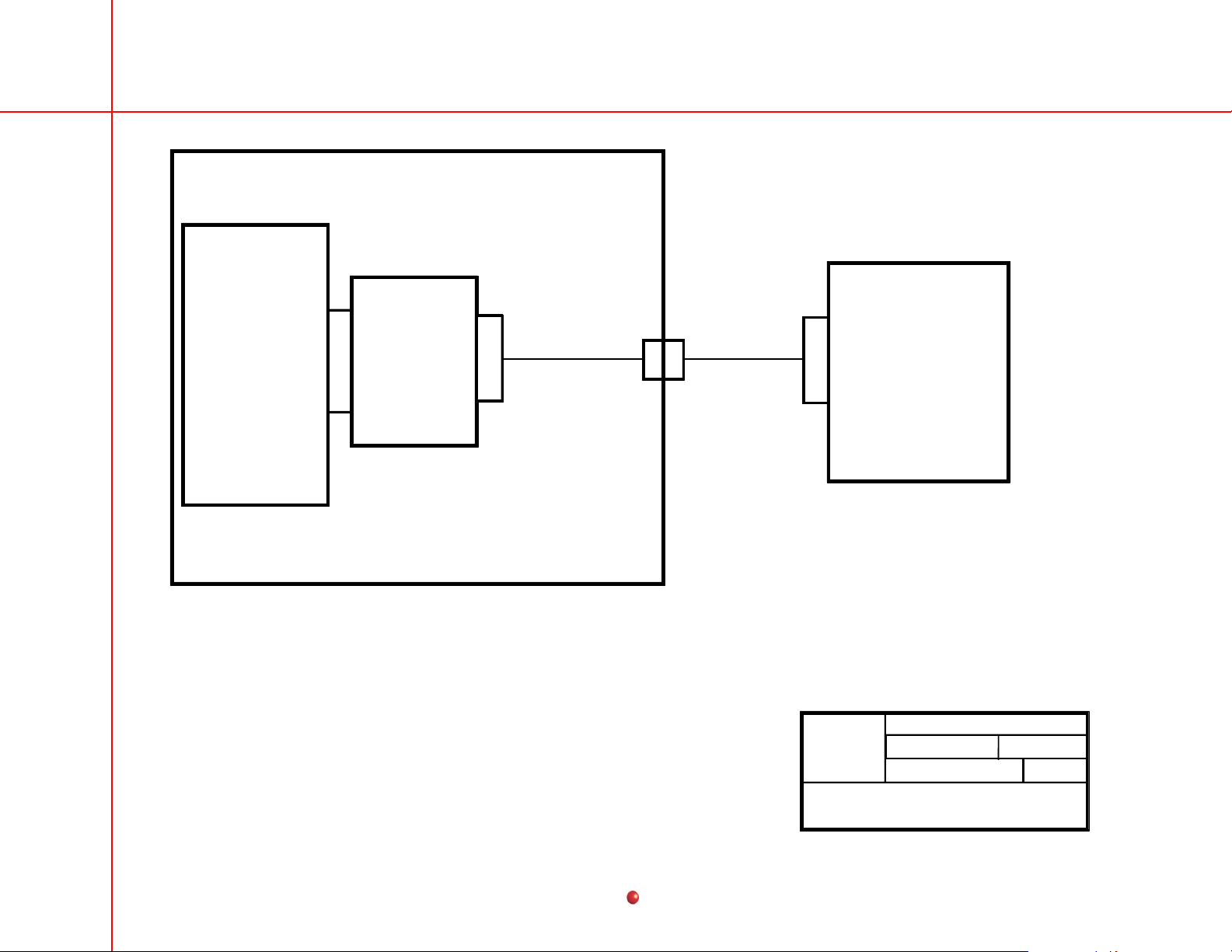
Functional Block Diagrams Released 11/00
PCI BUS
SLOT 5
P11
HOST
PENTIUM
CPU or
PASSIVE
BACKPLANE
DISPLAY
ADAPTER PCB
881447
LPT PORT
P3J3
CODONICS PRINTER
OR
LENZAR CAMERA
LPT PORT
ELECTRONICS BOX
9800 WORKSTATION
g
Codonics Printer/Lenzar Camera
Functional Block 66 – Codonics Printer/Lenzar Camera (1 of 1)
Contents
9800
GE OEC Training
COD_LENZ.DSF
Page 1 of 1
Functional Diagram
11/00
69
Page 70

Functional Block Diagrams Released 11/00
PCI BUS
HOST
PENTIUM
CPU or
PASSIVE
BACKPLANE
SLOT 8
ETHERNET
00-901551
BOARD
EXTERNAL
INTERFACE PCB
00-879184
P6
REAR
PANEL
P5
RJ 45
CONNECTOR
TO HOSPITAL NETWORK
or
ASPECT DDPI to PRINTER OPTION
ELECTRONICS BOX
9800 WORKSTATION
Functional Block 67 – DICOM/DDPI (1 of 1)
Contents
ASPECT DDPI
00-881505
The Aspect DDPI (Direct Digital Printer Interface)
receives DICOM information print as an input and
supplies a standard 3M M952 or P831, or
Kodak KCL digital print output
GE OEC Training
g
DICOM.DSF
DICOM/DDPI
Functional Diagram
PRINTER
9800
Page 1 of 1
11/00
70
 Loading...