

Page 1

Artisan Technology Group is your source for quality
new and certied-used/pre-owned equipment
• FAST SHIPPING AND
DELIVERY
• TENS OF THOUSANDS OF
IN-STOCK ITEMS
• EQUIPMENT DEMOS
• HUNDREDS OF
MANUFACTURERS
SUPPORTED
• LEASING/MONTHLY
RENTALS
• ITAR CERTIFIED
SECURE ASSET SOLUTIONS
SERVICE CENTER REPAIRS
Experienced engineers and technicians on staff
at our full-service, in-house repair center
Instra
Remotely inspect equipment before purchasing with
our interactive website at www.instraview.com
Contact us: (888) 88-SOURCE | sales@artisantg.com | www.artisantg.com
SM
REMOTE INSPECTION
View
WE BUY USED EQUIPMENT
Sell your excess, underutilized, and idle used equipment
We also offer credit for buy-backs and trade-ins
www.artisantg.com/WeBuyEquipment
LOOKING FOR MORE INFORMATION?
Visit us on the web at www.artisantg.com for more
information on price quotations, drivers, technical
specications, manuals, and documentation
Page 2

GE
Intelligent Platforms
Hardware Reference
C2K* 6U CPCI
Single Board Computer
Publication No: 70000524-800 Rev. C
Artisan Technology Group - Quality Instrumentation ... Guaranteed | (888) 88-SOURCE | www.artisantg.com
Page 3

Document History
Hardware Reference Document Number: 70000524-800 Rev. C
September 30, 2011
Artisan Technology Group - Quality Instrumentation ... Guaranteed | (888) 88-SOURCE | www.artisantg.com
Page 4

Chapter 1: Introduction
1.1 Overview .......................................................................................................................... 1-1
1.2 Specifications ................................................................................................................... 1-3
1.3 Compliance ...................................................................................................................... 1-4
1.4 C2K GPIO DC Electrical Characteristics ......................................................................... 1-4
1.5 Block Diagram ................................................................................................................. 1-5
1.6 Technical Support ............................................................................................................ 1-7
1.7 Related Documents ......................................................................................................... 1-7
Chapter 2: Installation
2.1 What Is Included .............................................................................................................. 2-1
2.2 Equipment Needed .......................................................................................................... 2-1
2.3 Power Requirements ....................................................................................................... 2-2
2.4 Configurations Jumpers ................................................................................................... 2-2
2.4.1 FLASH_WP# (P6) ................................................................................................ 2-2
2.4.2 EM_BOOTSEL# (P7) ........................................................................................... 2-2
2.4.3 PCI VIO Select (P9, P12) ..................................................................................... 2-2
2.4.4 COP_EN (P10) .................................................................................................... 2-3
2.4.5 C8051 Debug (P11) ............................................................................................. 2-3
2.4.6 Header/Jumper Locations .................................................................................... 2-3
2.5 Installation ........................................................................................................................ 2-3
2.5.1 C2K C-style Installation ........................................................................................ 2-3
2.5.2 C2K N-style Installation ........................................................................................ 2-4
2.6 U-Boot Utility .................................................................................................................... 2-7
2.6.1 Installation ............................................................................................................ 2-7
2.6.2 Initialization .......................................................................................................... 2-7
2.6.3 Commands ........................................................................................................... 2-7
2.6.4 Information Commands ........................................................................................ 2-9
2.6.5 Memory Commands ........................................................................................... 2-10
2.6.6 Flash Memory Commands ................................................................................. 2-11
2.6.7 Execution Control Commands ........................................................................... 2-12
2.6.8 Download Commands ........................................................................................ 2-12
2.6.9 Environment Variables Commands ................................................................... 2-13
2.6.10 Miscellaneous Commands ................................................................................. 2-14
Table of Contents
C2K User’s Guide 3
Artisan Technology Group - Quality Instrumentation ... Guaranteed | (888) 88-SOURCE | www.artisantg.com
Page 5

Chapter 3: Interfaces
3.1 Front Panel ...................................................................................................................... 3-1
3.2 Connectors ....................................................................................................................... 3-2
3.2.1 Connector Locations ............................................................................................ 3-2
3.2.2 CompactPCI Connector Pin Assignments ........................................................... 3-4
3.2.3 PMC Connector Pin Assignments ...................................................................... 3-10
3.2.4 COP Port (J6) Pin Assignments ......................................................................... 3-14
3.2.5 JTAG Port (J7) Pin Assignments ....................................................................... 3-14
3.2.6 Front-panel USB (USB4) Connector (J8) Pin Assignments ............................... 3-15
3.2.7 Serial I/O COM Port Termination Header (P15) Pin Assignments ..................... 3-15
3.3 Front-panel LEDs ........................................................................................................... 3-16
Chapter 4: Functional Blocks
4.1 Processor ......................................................................................................................... 4-1
4.2 DDR SDRAM ...................................................................................................................4-1
4.3 Flash Memory .................................................................................................................. 4-1
4.3.1 Flash Write Protection .......................................................................................... 4-1
4.3.2 Boot Code Selection ............................................................................................ 4-3
4.4 PCI Busses ...................................................................................................................... 4-3
4.5 Device Bus ....................................................................................................................... 4-4
4.6 SMBus ............................................................................................................................. 4-4
4.7 Gigabit Ethernet ............................................................................................................... 4-4
4.8 Serial I/O .......................................................................................................................... 4-5
4.8.1 Serial RS-232/422 Ports—COM1, COM2 ............................................................ 4-5
4.8.2 Serial RS-232/422 Ports—COM3, COM4 ............................................................ 4-5
4.8.3 Serial RS-422/485 Ports—COM5–COM8 ............................................................ 4-5
4.9 USB Ports ........................................................................................................................ 4-6
4.10 General-Purpose I/O ........................................................................................................4-6
4.11 Serial ATA I/O .................................................................................................................. 4-6
4.12 Counter/Timers ................................................................................................................ 4-7
4.12.1 Watchdog Timer ................................................................................................... 4-7
4.13 FPGA ............................................................................................................................... 4-8
4.13.1 System Management Interrupt ............................................................................. 4-8
4.14 RTC .................................................................................................................................. 4-9
4.15 CompactPCI Backplane Interface .................................................................................... 4-9
4.16 IPMI and Hot Swap ........................................................................................................ 4-11
4.16.1 Hot Swap Controller ........................................................................................... 4-11
4.16.2 CPLD ................................................................................................................. 4-11
4.16.3 PCI 6254 cPCI Bus Bridge ................................................................................. 4-11
4.16.4 C8051 Microcontroller ........................................................................................ 4-11
4.17 PMC Sites ...................................................................................................................... 4-14
4.17.1 PMC0 Site Features ........................................................................................... 4-14
4.17.2 PMC1 Site Features ........................................................................................... 4-15
4.18 Temperature Sensor ...................................................................................................... 4-15
4.19 Interrupt Circuitry ........................................................................................................... 4-15
4.20 EEPROMS ..................................................................................................................... 4-16
4 C2K User’s Guide
Artisan Technology Group - Quality Instrumentation ... Guaranteed | (888) 88-SOURCE | www.artisantg.com
Page 6

4.21 JTAG Boundary Scan Circuitry ...................................................................................... 4-17
4.21.1 Configuration Headers ....................................................................................... 4-17
Chapter 5: Resources
5.1 Memory and I/O Address Mapping .................................................................................. 5-1
5.1.1 PCI Buses ............................................................................................................ 5-1
5.1.2 SMBus ................................................................................................................. 5-2
5.1.3 Device Bus ........................................................................................................... 5-2
5.1.4 Multi-Purpose Pins (MPP) .................................................................................... 5-3
5.2 FPGA Registers ............................................................................................................... 5-4
5.2.1 Main Registers ..................................................................................................... 5-7
5.2.2 Interrupt Registers ............................................................................................. 5-11
5.2.3 GPIO Registers .................................................................................................. 5-16
5.2.4 Counter/timers ................................................................................................... 5-37
5.2.5 USART Registers ............................................................................................... 5-45
5.2.6 Standard USART Registers ............................................................................... 5-46
5.2.7 USART Divisor Latch Registers ......................................................................... 5-53
5.3 Component Locations .................................................................................................... 5-54
Chapter 6: Transition Module C2K-TM
6.1 Overview .......................................................................................................................... 6-1
6.2 Physical Description ......................................................................................................... 6-2
6.3 Block Diagram .................................................................................................................. 6-3
6.4 Connector Pin Assignments ............................................................................................. 6-4
6.4.1 CompactPCI Connectors ..................................................................................... 6-4
6.4.2 Ethernet Connectors (J6, J7, and J8) .................................................................. 6-7
6.4.3 Serial ATA Connectors (P19, P20) ...................................................................... 6-7
6.4.4 USB Connectors (J9, J10, and J11) .................................................................... 6-8
6.4.5 Serial RS-232 Connectors—COM1, COM2 (P15, P16) ....................................... 6-8
6.4.6 Serial RS-422/485—COM1–COM8 (P1–P8) ....................................................... 6-9
6.4.7 Serial RS-232—COM3, COM4 (P9, P10) ............................................................ 6-9
6.4.8 BATT+ Header (P13) ........................................................................................... 6-9
6.4.9 ICMB Interface Header (P17) ............................................................................ 6-10
6.4.10 GPIO Connector (P14) ....................................................................................... 6-10
6.4.11 Misc. Connector (P18) ....................................................................................... 6-11
6.4.12 PMC I/O Connectors (P11 and P12) .................................................................. 6-12
6.5 Connector Locations ...................................................................................................... 6-13
6.6 TM Schematics .............................................................................................................. 6-14
Index
C2K User’s Guide 5
Artisan Technology Group - Quality Instrumentation ... Guaranteed | (888) 88-SOURCE | www.artisantg.com
Page 7

List of Figures
Figure 1-1 C2K Block diagram (a) ........................................................................................................ 1-5
Figure 1-2 C2K Block diagram (b) ........................................................................................................ 1-6
Figure 2-1 C2K (C-style) with PMC modules installed ......................................................................... 2-5
Figure 2-2 C2K (N-style) with PMC modules installed ......................................................................... 2-6
Figure 3-1 Front panels: a. C-style; b. N-style...................................................................................... 3-1
Figure 3-2 Connector locations (C-style).............................................................................................. 3-2
Figure 3-3 Connector locations (N-style).............................................................................................. 3-3
Figure 3-4 USB front-panel connector (J8) pinout.............................................................................. 3-15
Figure 3-5 Front-panel LEDs.............................................................................................................. 3-16
Figure 4-1 Watchdog timer circuitry...................................................................................................... 4-8
Figure 4-2 SMI processing ................................................................................................................... 4-9
Figure 4-3 Interrupt circuitry ............................................................................................................... 4-16
Figure 4-4 JTAG circuitry.................................................................................................................... 4-18
Figure 5-1 C2K component locations (primary side) .......................................................................... 5-54
Figure 5-2 C2K component locations (secondary side)...................................................................... 5-55
Figure 6-1 C2K-TM block diagram ....................................................................................................... 6-3
Figure 6-2 Ethernet RJ-45 connector pinout ........................................................................................ 6-7
Figure 6-3 SATA connector pinout ....................................................................................................... 6-7
Figure 6-4 USB connector pinout ......................................................................................................... 6-8
Figure 6-5 Serial RS-232 DB9 connector pinout .................................................................................. 6-8
Figure 6-6 C2K-TM connector locations............................................................................................. 6-13
C2K User’s Guide 6
Artisan Technology Group - Quality Instrumentation ... Guaranteed | (888) 88-SOURCE | www.artisantg.com
Page 8

List of Tables
Table 1-1 C2K GPIO DC Electrical Characteristics..............................................................................1-4
Table 3-1 cPCI connector J1 pin assignments .....................................................................................3-4
Table 3-2 CompactPCI connector J2 pin assignments ........................................................................3-5
Table 3-3 CompactPCI connector J3 pin assignments ........................................................................3-6
Table 3-4 cPCI connector J4 pin assignments .....................................................................................3-7
Table 3-5 CompactPCI connector J5 pin assignments ........................................................................3-8
Table 3-6 PMC0_J11 and PMC0_J12 pin assignments..................................................................... 3-10
Table 3-7 PMC0_J13 and PMC0_J14 pin assignments..................................................................... 3-11
Table 3-8 PMC1_J21 and PMC1_J22 pin assignments..................................................................... 3-12
Table 3-9 PMC1_J23 and PMC1_J24 pin assignments..................................................................... 3-13
Table 3-10 COP Port (J20) pin assignments........................................................................................3-14
Table 3-11 JTAG Port (J7) pin assignments ........................................................................................3-14
Table 3-12 Front-panel Ethernet connector (J8) pin assignment .........................................................3-15
Table 3-13 Serial I/O COM port termination header (P15) pin assignments ........................................3-15
Table 4-1 Gigabit Ethernet on-board indicator LEDs. ..........................................................................4-4
Table 4-2 USB on-board indicator LEDs ..............................................................................................4-6
Table 4-3 SATA on-board activity indicator LEDs ................................................................................4-7
Table 4-4 C8051 external I/O ports pin assignments ......................................................................... 4-12
Table 4-5 I/O controller pin assignments............................................................................................4-13
Table 5-1 PCI local bus configuration ..................................................................................................5-1
Table 5-2 SMBus addressing ...............................................................................................................5-2
Table 5-3 Device bus devices, access, size and default address range ..............................................5-2
Table 5-4 MV64460 System Controller MPP pin assignments ............................................................5-3
Table 5-5 FPGA memory map - 16-bit Chip Select..............................................................................5-4
Table 5-6 FPGA memory map - 8-bit Chip Select................................................................................5-7
Table 5-7 Main registers.......................................................................................................................5-7
Table 5-8 Interrupt summary registers ...............................................................................................5-11
Table 5-9 GPIO registers ...................................................................................................................5-16
Table 5-10 Counter/timer registers.......................................................................................................5-37
C2K User’s Guide 7
Artisan Technology Group - Quality Instrumentation ... Guaranteed | (888) 88-SOURCE | www.artisantg.com
Page 9

Table 5-11 USART Resister .................................................................................................................5-45
Table 5-12 Standard 16550-compatible USART registers ...................................................................5-46
Table 5-13 Baud-rate divisor settings ...................................................................................................5-53
Table 6-1 CompactPCI connector J3 pin assignments ........................................................................6-4
Table 6-2 cPCI connector J4 pin assignments .....................................................................................6-5
Table 6-3 CompactPCI connector J5 pin assignments ........................................................................6-6
Table 6-4 Ethernet RJ-45 rear-panel connectors (J6, J7, J8) pin assignments ...................................6-7
Table 6-5 Serial ATA connectors (P19, P20) pin assignments ............................................................6-7
Table 6-6 USB connectors (J9, J10, and J11) pin assignments...........................................................6-8
Table 6-7 COM1 (P15) and COM2 (P16) pin assignments ..................................................................6-8
Table 6-8 COM1 (P1) through COM8 (P8) pin assignments ................................................................6-9
Table 6-9 COM3 (P9) and COM4 (P10) pin assignments ....................................................................6-9
Table 6-10 BATT+ header (P13) pin assignment ...................................................................................6-9
Table 6-11 ICMB interface header (P17) pin assignment ....................................................................6-10
Table 6-12 GPIO on-board header (P2) pin assignments ....................................................................6-10
Table 6-13 JTAG header (P18) pin assignments .................................................................................6-11
Table 6-14 PMC0_P11 and PMC1_P12 pin assignments....................................................................6-12
C2K User’s Guide 8
Artisan Technology Group - Quality Instrumentation ... Guaranteed | (888) 88-SOURCE | www.artisantg.com
Page 10

Chapter 1: Introduction
1.1 Overview
The C2K* is a 6U PICMG 2.16 compatible Single Board Computer intended for both system controller and peripheral slot applications. The board provides a CPU core, PICMG 2.16 compatible
backplane interface, and several peripheral devices/interfaces. The CPU core circuitry consists of
a Freescale MPC7448 or MPC7447A CPU operating at up to 1.4GHz, the Marvell® MV64460
PCI controller, up to 1GB of 167MHz DDR system memory, up to 512MB of boot memory, and
general support logic. An expanded feature list is below.
• 6U PICMG 2.16 compatible Single Board Computer, with full hot-swap support per
PICMG 2.1.
• IPMI controller with IPMB0 serial interface, per PICMG 2.9. Peripheral and BMC functions.
• 500MHz to 1.4GHz MPC7448 CPU, or 500MHz to 1.0GHz MPC7447A CPU with
Marvell MV64460 PCI Controller.
• Up to two 512MB banks of 167MHz DDR SDRAM, with ECC.
• PLX PCI 6254 PCI-to-PCI Interface for CPCI backplane.
• Two selectable 115kbps RS-232 or 2Mbps source-synchronous RS-422 ports available to
the backplane connectors.
• Six additional 460kbps source-synchronous RS-422/485 ports available to the backplane
connectors.
• Two 10/100/1000T Ethernet ports available to the backplane connector J3, wired per
PICMG 2.16.
• One 10/100/1000T Ethernet port available to the backplane J4.
• One 64-bit, PCI 33/66MHz or PCI-X 133MHz PMC site, with selectable +3.3V/+5.0V
VIO.
• One 64-bit PCI 33/66MHz PMC site with selectable +3.3V/+5.0V VIO.
• One bank of 64MB to 512MB Boot FEPROM with protected area feature.
• Three USB2.0 ports to the backplane connectors.
• One USB2.0 port to the front panel, on convection models.
• Thermal probe to monitor CPU die temperature and board ambient temperature.
• Sixteen 32-bit general-purpose counter/timers.
• Real Time Clock
• Two 1.5Gbps SATA 1.0 ports to the backplane.
• N-style and C-style versions.
C2K User’s Guide 1-1
Artisan Technology Group - Quality Instrumentation ... Guaranteed | (888) 88-SOURCE | www.artisantg.com
Page 11

Introduction
C2K Transition Module
GEIP offers an optional C2K Transition Module (C2K-TM) with the following on-board and
rear-panel connections:
• BATT+ (P13)—on-board 2 x 5 connector
• ETH0 (J6)—rear-panel RJ-45 connector
• ETH1 (J7)—rear-panel RJ-45 connector
• ETH2 (J8)—rear-panel RJ-45 connector
• GPIO connector (P14)—on-board 2 x 10-pin header
• ICMB interface (P17)—on-board 2 x 5-pin header
• Misc. Control header (P18)—on-board 2 x 5-pin header
• PMC0 I/O (P11)—on-board 2 x 32-pin header
• PMC1 I/O (P12)—on-board 2 x 32-pin header
• Reset switch, (S1)—rear-panel manual hardware reset micro-switch
• SATA1 (P19)—rear-panel connector
• SATA2 (P20)—rear-panel connector
• Serial I/O: COM1, COM2 RS-232 (P15, P16)—rear-panel DB9 connectors
• Serial I/O: COM3, COM4 RS-232 (P10, P9)—on-board 2 x 5-pin headers
• Serial I/O: COM1–COM4 RS-422 (P1–P4)—on-board 2 x 5-pin headers
• Serial I/O: COM5–COM8 RS-485 (P5–P8)—on-board 2 x 5-pin headers
• USB1 (J9)—rear-panel Type A USB connector
• USB2 (J10)—rear-panel Type A USB connector
• USB3 (J11)—rear-panel Type A USB connector
1-2 C2K User’s Guide
Artisan Technology Group - Quality Instrumentation ... Guaranteed | (888) 88-SOURCE | www.artisantg.com
Page 12

1.2 Specifications
Physical Description
Form Factor: 6U per PICMG 2.16
Height: 233.20 ± 0.15 mm (9.1811 ± 0.0059 in.)
Depth: 159.85 ± 0.15 mm (6.2933 ± 0.0059 in.)
Weight
C-style:
N-style:
Power Requirements
+5V, +3.3V, +12V: Required from the cPCI backplane
±12V: As required by installed PMC modules
TBD
TBD
NOTE: The +12V requires 10mA for the Hot Swap circuitry which is
otherwise not used by the board.
Introduction
Power Consumption
Peak: 5.7A 4.10A
Idle: TBD TBD
Inrush: 2.0A @ 120µs 2.0A @ 120µs
BATT+: 10µA
Total: 42W
* Measured at VxWorks® prompt
+5V +3.3V
Temperature (operating)
C-style: 0° C to 70° C (ambient)
N-style: -40° C to 85° C
Temperature (storage)
C-style: -40° C to 85° C
N-style: -55° C to 105° C
Relative Humidity - @ 40° C (non-condensing)
C-style: 5–95% @ 40° C
N-style: 5–95% @ 40° C
Shock (half-sine)
C-style: 20g peak / 6ms (3 axes, up & down, 3 hits / direction)
N-style: 40g peak / 11ms (3 axes, up & down, 3 hits / direction),
100g peak / 6ms (3 axes, up & down, 3 hits / direction)
Vibration (random)
C-style: 0.04g2 / Hz @ 5-100Hz (2g rms), 60 min. / axis
N-style: 0.1g2 / Hz @ 5-2000Hz (12g rms), 60 min. / axis
C2K User’s Guide 1-3
Artisan Technology Group - Quality Instrumentation ... Guaranteed | (888) 88-SOURCE | www.artisantg.com
Page 13

1.3 Compliance
MTBF
Calculations are available in accordance with MIL-HDBK-217.
Please contact GEIP for latest values.
Safety
Designed to meet standard UL1950/60950
Emissions
Designed to meet FCC Part15, SubPart A
1.4 C2K GPIO DC Electrical Characteristics
Introduction
Table 1-1 C2K GPIO DC Electrical Characteristics
Symbol Parameter Min Max Unit
GPIO
Igpio GPIO source current 12 mA
lgpio GPIO sink current 12 mA
Vih GPIO input high voltage 2.0 5.5 V
Vil GPIO input low voltage 0.8 V
Voh GPIO output high voltage 2.4 V
Vol GPIO output low voltage 0.4
Unit Supply Current and Power Dissipation
Ppmc
Maximum Power available to each PMC site, sum of
+5.0V and +3.3V powers
7.5 W
1-4 C2K User’s Guide
Artisan Technology Group - Quality Instrumentation ... Guaranteed | (888) 88-SOURCE | www.artisantg.com
Page 14

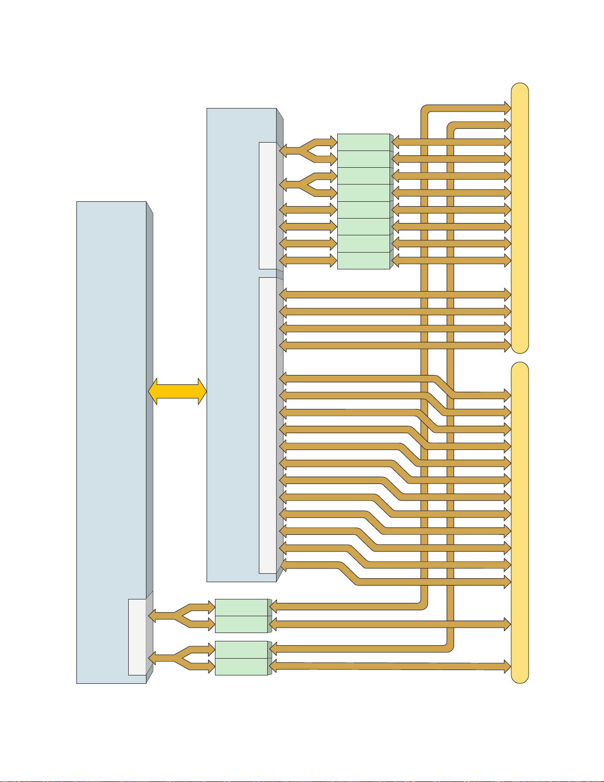
1.5 Block Diagram
MPC7448
G4
Processor
512KB
L2 Cache
MPX
Bus
167MHz
MV64460
PowerPC
System
Controller
DDR
SDRAM
Mem Bus
167MHz
PCI Bus 0
64-bit 33/66MHz64-bit 33/66MHz
RGMII0
RGMII1
RGMII2
COP (J6)
PCI Bus 0
or 133MHz
PCI-X
PCI 6254
cPCI
Bridge
PMC0
J11
J12
J13
J14
VSC8244
Gigabit
Ethernet
PHY
JTAG_J7
to
JTAG
Scan
Chain
cPCI bus
ETH0
ETH1
ETH2
Introduction
cPCI_J1
cPCI_J2
cPCI_J3
cPCI_J3
cPCI_J4
PCI Bus 1
64-bit 33/66MHz
Tem p
Sensor
Board
Config.
EEPROM
User
EEPROM
RTC
Device Bus
Flash
ROM
(soldered)
PMC1
J21
J22
J23
J24
PCI2050B
PCI/PCI
Bridge
GD31244
SATA
Controller
FPGA
SATA 1
SATA 2
ISP 1563
USB 2.0
Controller
8051
IPMC
Hot
Swap
Ctlr
cPCI_J5
USB1
USB2
USB3
Figure 1-1 C2K Block diagram (a)
C2K User’s Guide 1-5
Artisan Technology Group - Quality Instrumentation ... Guaranteed | (888) 88-SOURCE | www.artisantg.com
Page 15
MV64460
PowerPC
System
Controller
FPGA
USART
COM3
COM4
COM5
COM6
COM7
COM8
GPIO0
GPIO1
GPIO2
GPIO3
RS-232 I/F
RS-422 I/F
RS-232 I/F
RS-422 I/F
RS-422 I/F
RS-485 I/F
RS-485 I/F
RS-485 I/F
RS-485 I/F
Introduction
cPCI_J4
MPSC
Device
Bus
UART0
UART1
GPIO
RS-422 I/F
RS-232 I/F
RS-422 I/F
RS-232 I/F
GPIO4
GPIO5
GPIO6
GPIO7
GPIO8
GPIO9
GPIO10
GPIO11
GPIO12
GPIO13
GPIO14
GPIO15
COM1 (RS-422)
COM1 (RS-232)
COM2 (RS-422)
COM2 (RS-232)
cPCI_J5
Figure 1-2 C2K Block diagram (b)
1-6 C2K User’s Guide
Artisan Technology Group - Quality Instrumentation ... Guaranteed | (888) 88-SOURCE | www.artisantg.com
Page 16

Introduction
1.6 Technical Support
Most issues can be resolved by referring to this manual. If any problems cannot be resolved,
please contact GEIP Technical Support:
If products must be returned, contact GE for a Return Material Authorization (RMA) Number.
This RMA Number must be obtained prior to any return.
RMA request forms can be obtained from:
www.ge-ip.com/rma
GE Technical Support is available at: 1-800-433-2682 in North America,
or +1-780-401-7700 for international calls. Requests for Technical Support can be sent to:
support.huntsville.ip@ge.com
Or, visit our website:
www.ge-ip.com
1.7 Related Documents
For more information on C2K components, refer to the following documents:
Components
• MPC7448 RISC Microprocessor Hardware Specifications—Motorola® Inc., MPC7448EC
Rev. 2, February 2004
• MV64460, MV64461, MV64462 System Controller Hardware Specification - Parts 1 &
2—Marvell Semiconductor, Inc.®, Doc. no. MV-S101286-00(01) Rev B, July 2004
• PCI 6254 (HB6) Dual Mode Universal PCI-to-PCI Bridge DataBook—PLX Technology,
Inc., Version 2.0, May 2003
• PCI2050B PCI-to-PCI Data Manual—Texas Instruments Incorporated, SCPS076E,
November 2004
• ISP1563 Hi-Speed USB PCI Host Controller Product Data—Philips Semiconductors, Document Order Number 9397 750 14244 Rev 01, July 2005
• Intel® 31244 PCI-X to Serial ATA Controller Datasheet—Intel Corporation, Document
Number 273595-005, April 2004
• VSC8244 Quad Port 10/100/1000Base-T PHY with RGMII / RTBI MAC Interfaces—Vitesse Semiconductor Corporation, PB-VSC8244-002, September 2004
• 512Mb: x4, x8, x16, DDR SDRAM Datasheet—Micron Technology, Inc., Rev G 4/04 EN,
April 2004
• Spartan-3E FPGA Family: Complete Data Sheet—Xilinx, Inc., DS312, March 2005
• S29GLxxxN MirrorBit™ Flash Family S29GL512N, S29GL256N, S29GL128N, Data
Sheet—AMD Spansion
• S29GLxxxM MirrorBit™ Flash Family S29GL256M, S29GL128M, S29GL064M,
S29GL032M Data Sheet—AMD Spansion, Publication Number: S29GLxxxM_00 Revi
sion A Amendment 4, March 2004
-
C2K User’s Guide 1-7
Artisan Technology Group - Quality Instrumentation ... Guaranteed | (888) 88-SOURCE | www.artisantg.com
Page 17

• C8051F120/1/2/3/4/5/6/7 C8051F130/1/2/3 Mixed Signal ISP Flash MCU Family—Silicon Laboratories Inc., Rev 1.3, August 2004
• M41T62 Serial Access Real-Time Clock with Alarms - STMicroelectronics, Rev 10.0,
November 2005
• LTC4244/LTC4244-1 Rugged, CompactPCI Bus Hot Swap Controllers—Linear Technology Corporation, 42441f, February 2004
• Maxim MAX6657/MAX6658/MAX6659 ±1°C, SMBus-Compatible Remote/Local Temperature Sensors with Overtemperature Alarms—Maxim Integrated Products, 19-2034;
Rev. 2, March 2002
Specifications
• ICMB 1.0 Rev 1.3—Intelligent Chassis Management Bus Bridge Specification, April
2003.
• IEEE Std. 802.3-2002—IEEE Standard for Information Technology- Telecommunications
and information exchange between systems- Local and metropolitan area networks - Specific requirements Part 3: Carrier sense multiple access with collision detection
(CSMD/CD) access method and physical layer specifications, March 2002.
• IEEE Std. 1101.2-1992(2001)—IEEE Standard for Mechanical Core Specifications for
Conduction-Cooled Eurocards, January 1993.
• IEEE Std. 1101.10-1996—IEEE Standard for Additional Mechanical Specifications for
Microcomputers using the IEEE Std 1101.1-1991 Equipment Practice, December 1996.
• IEEE Std. 1149.1-1990—IEEE Standard Test Access Port and Boundary Scan Architecture, June 1993.
Introduction
• IEEE Std. 1284-2000—IEEE Standard Signaling Method for a Bidirectional Parallel
Peripheral Interface for Personal Computers, September 2000.
• IEEE1386-2001—IEEE Standard for a Common Mezzanine Card (CMC) Family, June,
2001.
• IEEE1386.1-2001—IEEE Standard Physical and Environmental Layers for PCI Mezzanine Cards (PMC), June, 2001.
• IEEE Std. 802.3-2002—Part 3: Carrier Sense Multiple Access Collision Detection
(CSMA/CD) Access Method and Physical Layer Definitions, March 2002.
• Intel, Universal Host Controller Interface (UHCI) Design Guide, Revision 1.1,
297650-002.
• IPC-A-610—Acceptability of Electronic Assemblies, Revision C, January 2000.
• IPC-6012A with Amendment 1—Qualification and Performance Specification for Rigid
Printed Boards, July 2000.
• PICMG 2.0 Rev 3.0—CompactPCI Specification, October 1999.
• PICMG 2.1 Rev 2.0—Hot Swap Specification, January 2001
• PICMG 2.16 Rev 1.0—Packet Switching Backplane Specification, September 2001
• PICMG 2.3 Rev 1.0—PMC on CompactPCI Specification, August, 1998.
• PICMG 2.9 Rev 1.0—CompactPCI System Management Specification, February, 2000.
• PCI Special Interest Group—PCI Local Bus Specification, Revision 2.3, October 2001.
1-8 C2K User’s Guide
Artisan Technology Group - Quality Instrumentation ... Guaranteed | (888) 88-SOURCE | www.artisantg.com
Page 18

Introduction
• PCI Special Interest Group—PCI-X Local Bus
• Phillips Semiconductors—The I2C Specification, version 2.1, document 9398-393-40011,
January 2000.
• TIA / EIA-232-F-1997, Telecommunications Industry Association—Interface Between
Data Terminal Equipment and Data Circuit-Terminating Equipment Employing Serial
Binary Data Interchange, October 1997.
• TIA / EIA-485-F-1997, Telecommunications Industry Association—
• VITA Standards Organization, VITA 20-2001—American National Standard for Conduction Cooled PMC, August, 2001.
• VITA Standards Organization, VITA 30.1-2002—American National Standard for 2mm
Connector Practice on Conduction Cooled Euroboards, August, 2002.
• VITA Standards Organization, VITA 32-2002—Processor PMC Standard for Processor
PCI Mezzanine Cards, September 2002.
• VITA Standards Organization, VITA 39-2003—PCIX Auxiliary Standard for PMCs and
Processor PMCs, August 2003.
• Universal Serial Bus Specification, Revision 2.0, April 2000.
1. PICMG Specifications are available to PICMG members only. GEIP is not authorized to distribute copies of
these specifications. More information can be found at http://www.picmg.org.
2. VITA Specifications are available to VITA members only. GEIP is not authorized to distribute copies of these
specifications. More information can be found at http://www.vita.com.
3. Data sheets from hardware components can be downloaded from individual vendors web sites.
C2K User’s Guide 1-9
Artisan Technology Group - Quality Instrumentation ... Guaranteed | (888) 88-SOURCE | www.artisantg.com
Page 19

Chapter 2: Installation
2.1 What Is Included
The C2K Single Board Computer (SBC) is shipped with the following items:
• C2K SBC Printed Circuit Assembly
2.2 Equipment Needed
The following items are needed to install and operate the C2K:
• C-style CompactPCI-compatible chassis
or
• N-style CompactPCI-compatible chassis
E.S.D.
Caution! Always use proper Electrostatic Discharge (ESD) protection when han-
dling printed circuit boards to avoid seriously damaging components. Product handlers must always be properly grounded.
C2K User’s Guide 2-1
Artisan Technology Group - Quality Instrumentation ... Guaranteed | (888) 88-SOURCE | www.artisantg.com
Page 20

Installation
2.3 Power Requirements
The C2K requires +5.0V and +3.3V from the CompactPCI backplane and Hot Swap functions
require +12V. Installed PMC modules may require ±12V.
2.4 Configurations Jumpers
The C2K provides the following configuration header/jumpers:
2.4.1 FLASH_WP# (P6)
P6 is a 2-pin Flash Write-Protect header/jumper that enables write-protection for the flash memory.
If a jumper is installed on P6, the FLASH_WP# signal is asserted preventing writes to the
flash ROM.
If a jumper is not installed on P6, the FLASH_WP# signal is de-asserted allowing writes the
flash ROM.
2.4.2 EM_BOOTSEL# (P7)
P7 is a 2-pin Emergency Boot Select header/jumper that determines which boot code the C2K will
execute after reset. Boot code provided by GEIP is stored in the upper 8MB of flash memory.
If a jumper is installed on the EM_BOOTSEL header (P7), the GEIP firmware will boot
from the GEIP provided emergency boot code stored in the Emergency Boot area of flash.
If a jumper is not installed on the EM_BOOTSEL header (P7), the firmware will jump to
user boot code area and begin executing custom boot code (see “Boot Code Selection” on
page 4-3).
2.4.3 PCI VIO Select (P9, P12)
P9 and P12 are 3-pin header/jumpers that set the VIO for PCI Busses (PMC sites) at +3.3V or
+5V. P12 controls the VIO for PCI Bus 0 (PMC0) and P9 controls VIO for PCI Bus 1 (PMC1).
If a jumper is installed on pins 1 and 2, the VIO is set to +3.3V.
If a jumper is installed on pins 2 and 3, the VIO is set to +5V
1. +3.3V
2. PMC VIO
3. +5V
12 3
C2K User’s Guide 2-2
Artisan Technology Group - Quality Instrumentation ... Guaranteed | (888) 88-SOURCE | www.artisantg.com
Page 21
Installation
2.4.4 COP_EN (P10)
P10 is a 2-pin COP Enable header/jumper that isolates the MPC7448 processor from the JTAG
Scan chain and connects the COP header (J6) to the processor to enable software debugging (see
“JTAG circuitry” on page 4-18).
If a jumper is installed on P10, the on-board COP header (J6) is connected to the MCP7448
processor for software debugging.
If a jumper is not installed on P10, the COP header (J6) is disconnected from the processor.
2.4.5 C8051 Debug (P11)
P11 is a 2-pin C8051 Debug header/jumper that isolates the C8051 Microcontroller from the
JTAG Scan chain to enable IPMI software debugging.
If a jumper is installed on P11, the C8051 debugging is enabled.
If a jumper is not installed on P11, the C8051 debugging is disabled.
2.4.6 Header/Jumper Locations
For header/jumper locations, please refer to Figure 3-2 on page 3-2.
NOTE: With the exception of the PCI Bus VIO Select header/jumpers (P9 and P12), none of the
preceding header/jumpers need to have a jumper installed for C2K initial power-up.
2.5 Installation
Caution! Do not attempt to install the C2K in a backplane where the J4 connector is
bused or routed in accordance with the CompactPCI H110 specification. The C2K is
equipped with an IEC key to prevent such installation but if the backplane is not
keyed, installation is still possible.
Caution! Do not attempt to install the C2K in a Fabric slot of a PICMG 2.16 Packet
Switching Backplane. The C2K is equipped with an IEC key to prevent such
installation, but if the backplane is not keyed installation is still possible.
2.5.1 C2K C-style Installation
1. Remove the C2K from the static-safe envelope (see “E.S.D. Caution” on page 2-1).
2-3 C2K User’s Guide
Artisan Technology Group - Quality Instrumentation ... Guaranteed | (888) 88-SOURCE | www.artisantg.com
Page 22

Installation
2. Install optional PMC module(s) per manufacturers instructions (see “PMC Sites” on
page 4-14 for restrictions).
3. Configure the PMC VIO using VIO configuration jumpers P9, P12 (see “PCI VIO Select
(P9, P12)” on page 2-2).
4. Install the C2K in a 6U C-style CompactPCI-compliant chassis.
5. Slide the C2K into the slot guide, applying even pressure to the upper and lower extraction
handles. Be careful not to bend connector pins.
NOTE: The C-style C2K is Hot Swap-compliant and can be installed in and removed from
a powered-on Hot Swap-compliant chassis.
After sliding the C2K in the slot guide until the card engages the pins, wait for the blue
front-panel Hot Swap LED to turn off before closing the ejector handle switch (bottom
ejector handle).
6. Push up on the lower extraction handle and down on the upper handle to seat the CompactPCI connectors in the backplane connectors. The red tab on the extraction handles should
“click” when the board is locked into the chassis.
7. Tighten the small phillips-head screws embedded in the upper and lower extraction handles
to secure the C2K to the chassis.
8. Apply power to the chassis.
NOTE: C2K can be installed in a system controller or peripheral slot. If the C2K is not installed
in a system slot, a system controller card must be installed in the system slot to supply a PCI reference clock to C2K.
2.5.2 C2K N-style Installation
1. Remove the C2K SBC from the static-safe envelope (see “E.S.D. Caution” on page 2-1).
2. Install optional PMC module(s) per manufacturers instructions (see “PMC Sites” on
page 4-14 for restrictions).
3. Configure the PMC VIO using VIO configuration jumpers P9, P12 (see “PCI VIO Select
(P9, P12)” on page 2-2).
4. Install the C2K in a 6U N-style CompactPCI-compliant chassis.
5. Slide the C2K into the slot guide, applying even pressure to the upper and lower extraction
handles. Be careful not to bend connector pins.
6. Tighten upper and lower Wedge-Loks™ to 115inch/ounces using a 3/32-inch hex driver.
This secures the C2K in the system chassis and ensures proper heat conduction. Do not
overtighten.
7. Apply power to the chassis.
NOTE: C2K can be installed in a system controller or peripheral slot. If the C2K is not installed
in a system slot, a system controller card must be installed in the system slot to supply a PCI reference clock to C2K.
C2K User’s Guide 2-4
Artisan Technology Group - Quality Instrumentation ... Guaranteed | (888) 88-SOURCE | www.artisantg.com
Page 23

PMC Module
Installation
PMC Module
Figure 2-1 C2K (C-style) with PMC modules installed
2-5 C2K User’s Guide
Artisan Technology Group - Quality Instrumentation ... Guaranteed | (888) 88-SOURCE | www.artisantg.com
Page 24
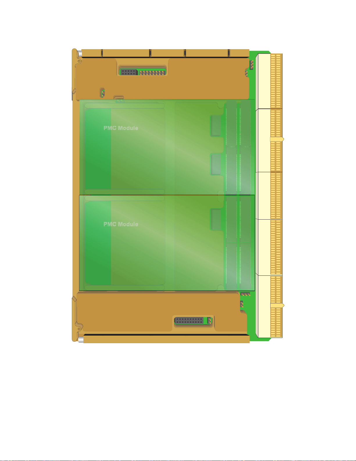
PMC Module
Installation
PMC Module
Figure 2-2 C2K (N-style) with PMC modules installed
C2K User’s Guide 2-6
Artisan Technology Group - Quality Instrumentation ... Guaranteed | (888) 88-SOURCE | www.artisantg.com
Page 25

Installation
2.6 U-Boot Utility
The C2K includes a universal boot loader (U-Boot) utility that is pre-installed in flash ROM.
U-Boot is designed to work with any operating system including Linux and VxWorks® and performs the following functions:
• Load the O/S kernel from Ethernet, user flash area, or USB
• Program the user flash
• Program the boot flash (self update)
• Load the O/S kernel from user flash
• Set the Real-Time Clock
• Save boot parameters in EEPROM
• Configure the MV64460 Memory Controller
2.6.1 Installation
The C2K is shipped with U-Boot pre-installed in flash memory.
2.6.2 Initialization
The C2K has been initialized during production and testing.
2.6.3 Commands
The following is a summary of commands the U-Boot utility uses for the C2K:
?
autoscr
base
bdinfo
boot boots default, e.g., run ‘bootcmd’
bootd boots default, e.g., run ‘bootcmd’
bootelf
bootm
bootp
bootvx
cmp
coninfo
cp
crc32
date
echo
erase
flinfo
alias for ‘help’
runs script from memory
prints or sets address offset
prints Board Info structure
boots from an ELF image in memory
boots application image from memory
boots image from the network using BootP/TFTP protocol
boots VxWorks from an ELF image
compares memory
prints console devices and information
copies memory
calculates checksum
gets / sets / resets date and time
echoes arguments to console
erases flash memory
prints flash memory information
2-7 C2K User’s Guide
Artisan Technology Group - Quality Instrumentation ... Guaranteed | (888) 88-SOURCE | www.artisantg.com
Page 26

Installation
to
help
iminfo
imls
loadb
loads
loop
md
mm
mtest
mw
nm
ping
printenv
protect
rarpboot
reset
run
saveenv
setenv
sleep
tfpboot
version
starts application at address ‘addr’
prints online help
prints header information for application image
lists all images found in flash
loads binary file over serial line (kermit mode)
loads S-Record file over serial line
performs infinite loop on address range
displays memory
modifies memory (auto-incrementing)
tests RAM
writes memory (fill)
modifies memory (constant address)
sends ICMP ECHO REQUEST to network host
prints environment variables
enables or disables flash write-protect
boots image from network using RARP/TFRP protocol
resets the CPU
runs commands in an environment variable
saves environment variables to a persistent storage
sets environment variables
delays execution for some time
boots image from network using TFTP protocol
prints monitor version
C2K User’s Guide 2-8
Artisan Technology Group - Quality Instrumentation ... Guaranteed | (888) 88-SOURCE | www.artisantg.com
Page 27

2.6.4 Information Commands
The following U-Boot commands provide information
bdinfo
C2K=> help bdinfo
bdinfo:
prints board information used by U-Boot, such as memory addresses and sizes, clock frequencies
and MAC addresses.
coninfo
C2K=> help coninfo
cp [.b, .w, .l] source target count:
displays console I/O device information.
flinfo
C2K=> help flinfo
flinfo:
Installation
prints information for all flash memory banks.
flinfo N:
prints information for flash memory bank # N.
iminfo
C2K=> help iminfo
iminfo addr [addr ...]:
prints header information for application image starting at address ‘addr’ in memory; this includes verification of the image contents (magic number, header and payload checksums).
imls
C2K=> help imls
imls:
prints information about all images found at sector boundaries in flash.
help
C2K=> help
help [command ...]:
shows help information (for ‘command’).
prints online help for the monitor commands.
without arguments, it prints a short usage message for all commands.
to get detailed information about specific commands, type ‘help’ with one or more command names
as arguments.
2-9 C2K User’s Guide
Artisan Technology Group - Quality Instrumentation ... Guaranteed | (888) 88-SOURCE | www.artisantg.com
Page 28

2.6.5 Memory Commands
base
C2K=> help base
base:
prints address offset from memory commands.
base off:
sets address offset for memory commands to ‘off’.
crc32
C2K=> help crd32
crc32 address count [addr]:
calculates CRC32 checksum [save at addr].
cmp
C2K=> help cmp
Installation
cmp [.b, .w, .l] adder1 addr2 count:
compares memory.
cp
C2K=> help cp
cp [.b, .w, .l] source target count:
copies memory.
md
C2K=> help md
md [.b, .w, .l] address [# of objects]:
displays memory.
mm
C2K=> help mm
mm [.b, .w, .l] address:
modifies memory, automatically increments address.
mtest
C2K=> help mtest
mtest [start [end [pattern]]]:
performs simple RAM read/write test.
C2K User’s Guide 2-10
Artisan Technology Group - Quality Instrumentation ... Guaranteed | (888) 88-SOURCE | www.artisantg.com
Page 29

mw
C2K=> help mw
mw [.b, .w, .l] address value [count]:
perform memory write.
nm
C2K=> help nm
nm [.b, .w, .l] address:
modifies memory, read and keep address.
loop
C2K=> help loop
loop [.b, .w, .l] address number_of_objects:
performs loop on a set of addresses.
2.6.6 Flash Memory Commands
erase
C2K=> help erase
Installation
erase start end:
erases flash from addr ‘start’ to addr ‘end’.
erase N:SF [-SL]:
erases sectors SF–SL in flash bank # N.
erase bank N:
erases flash bank # N.
erase all:
erases all flash banks.
protect
C2K=> help protect
protect on start end:
protects flash from addr ‘start’ to addr ‘end’.
protect on N:SD [-SL]:
protects sectors SF–SL in flash bank # N.
protect on bank N:
protects flash bank N.
protect on start all:
protects all flash banks.
2-11 C2K User’s Guide
Artisan Technology Group - Quality Instrumentation ... Guaranteed | (888) 88-SOURCE | www.artisantg.com
Page 30

protect off start end:
enables writes to flash from addr ‘start’ to addr ‘end’.
protect on N:SD [-SL]:
enables writes to sectors SF–SL in flash bank # N.
protect on bank N:
enables writes to flash bank N.
protect on start all:
enables writes to all flash banks.
2.6.7 Execution Control Commands
boot
C2K=> help boot
bootm
C2K=> help bootm
bootm [addr [arg...]]:
Installation
boots application image stored in memory passing argument ‘arg ...’; when booting a Linux kernel,
‘arg’ can be the address of an initrd image.
go
C2K=> help go
go addr[arg ...]:
starts application at address ‘addr’ passing ‘arg’ as arguments.
2.6.8 Download Commands
bootp
C2K=> help bootp
bootp [loadAddress] [bootfilename]:
bootelf
C2K=> help bootelf
bootelf [address]:
loads address of ELF image.
bootvx
C2K=> help bootvx
bootvx [address]:
loads address of VxWorks ELF image.
C2K User’s Guide 2-12
Artisan Technology Group - Quality Instrumentation ... Guaranteed | (888) 88-SOURCE | www.artisantg.com
Page 31

loadb
C2K=> help loadb
loadb [off] [baud]:
loads binary file over serial line with offset ‘off’ and baud rate ‘baud’.
loads
C2K=> help loads
loads [off] [baud]:
loads S-Record fileover serial line with offset ‘off’ and baud rate ‘baud’.
rarpboot
C2K=> help rarpboot
rarpboot [loadAddress] [bootfilename]:
prints values of all environment variables.
tftpboot
C2K=> help tftpboot
Installation
tftpboot [loadAddress] [bootfilename]:
2.6.9 Environment Variables Commands
printenv
C2K=> help printenv
printenv:
prints values of all environment variables.
printenv name ...
print value of environment variable ‘end’.
saveenv
C2K=> help saveenv
saveenv:
no help available.
setenv
C2K=> help setenv
setenv name value ...
sets environment variable ‘name’ to ‘value...’
setenv name:
deletes environment variable ‘name’.
2-13 C2K User’s Guide
Artisan Technology Group - Quality Instrumentation ... Guaranteed | (888) 88-SOURCE | www.artisantg.com
Page 32

run
C2K=> help run
run var [...]:
runs the commands in the environment variable(s) ‘var’.
bootd
C2K=> help bootd
bootd:
no help available
2.6.10 Miscellaneous Commands
ping
C2K=> help ping
ping pingaddress:
date
C2K=> help date
Installation
date [MMDDhhmm [CC]YY][.ss]:
date reset:
without arguments: prints data and time.
with arguments: sets the system date and time.
with ‘reset’ argument: resets the Real-Time Clock.
reset
C2K=> help reset
reset:
no help available.
sleep
C2K=> help sleep
sleep N:
delays execution for N seconds (N is _decimal_ !!!!).
version
C2K=> help version
version:
no help available.
C2K User’s Guide 2-14
Artisan Technology Group - Quality Instrumentation ... Guaranteed | (888) 88-SOURCE | www.artisantg.com
Page 33

Chapter 3: Interfaces
3.1 Front Panel
The C2K front-panel (C-style version only)
includes the following features:
• LEDs
• Two PMC front panel cutouts
• USB connector (J8)
• Recessed manual reset switch
LEDs: Hot Swap (blue), PWR (green), PBIT
(green), and User (yellow), 8051 (yellow).
PMC Cutouts: two cutouts to accommodate installed
PMC module front panels.
USB Connector: USB4—Type A USB connector
(J8).
Recessed Reset: provides access to a recessed reset
micro-switch for performing a manual hardware
reset.
TIP: A straightened paper clip can be
used to access the recessed reset button.
RESET
USB
USB
PMC1PMC1
PBIT
PWR
USER
PBIT
USER
IPMC
IPMC
PWR
HS
HS
b.a.
Figure 3-1 Front panels: a. C-style; b. N-style
C2K User’s Guide 3-1
Artisan Technology Group - Quality Instrumentation ... Guaranteed | (888) 88-SOURCE | www.artisantg.com
Page 34

3.2 Connectors
3.2.1 Connector Locations
Interfaces
J8
P7
P11
J7
P15
J21
J23
P6
P9
J22
J24J12
J5
J4
J3
J11
J2
J13
J14
P12
J1
P13
J6
P10
(Drawing not to scale)
Figure 3-2 Connector locations (C-style)
NOTE: The front-panel USB connector (J8) is only available on C-style versions of the C2K.
C2K User’s Guide 3-2
Artisan Technology Group - Quality Instrumentation ... Guaranteed | (888) 88-SOURCE | www.artisantg.com
Page 35

Interfaces
P7
J7
P11
P15
J21
J23
P6
P9
J22
J24J12
J5
J4
J3
J11
J13
J6
P10
Figure 3-3 Connector locations (N-style)
P12
P13
J2
J14
J1
3-3 C2K User’s Guide
Artisan Technology Group - Quality Instrumentation ... Guaranteed | (888) 88-SOURCE | www.artisantg.com
Page 36

Connector Legend
Interfaces
J1–J5: P6:
J11–J14: P11:
J21–J24: P12:
CompactPCI connectors ROM_WP#
COP header EM_BOOTSEL#
J6: P7:
JTAG header PMC1 VIO Selection header
J7: P9:
USB front-panel connector COP Interface Enable
J8: P10:
PMC0 site connectors C8051 Debug Enable
PMC1 site connectors PMC0 VIO Selection header
COM Port Termination header
P15:
3.2.2 CompactPCI Connector Pin Assignments
CPCI_J1 Pin Assignments
Table 3-1 cPCI connector J1 pin assignments
Pin A B C D E F
J1-25
J1-24
J1-23
J1-22
J1-21
J1-20
J1-19
J1-18
J1-17
J1-16
J1-15
J1-12–14
J1-11
J1-10
J1-9
J1-8
J1-7
J1-6
J1-5
J1-4
J1-3
J1-2
J1-1
+5V REQ64# ENUM# +3.3V +5V GND
AD1 +5V VIO AD0 ACK64# GND
+3.3V AD4 AD3 +5V AD2 GND
AD7 GND +3.3V AD6 AD5 GND
+3.3V AD9 AD8 M66EN C/BE0# GND
AD12 GND VIO AD11 AD10 GND
+3.3V AD15 AD14 GND AD13 GND
SERR# GND +3.3V PA R C/BE1# GND
+3.3V IPMB_SCL IPMB_SDA GND PERR# GND
DEVSEL# GND VIO STOP# LOCK# GND
+3.3V FRAME# IRDY# BD_SEL# TRDY# GND
AD18 AD17 AD16 GND C/BE2# GND
AD21 GND +3.3V AD20 AD19 GND
C/BE3# IDSEL AD23 GND AD22 GND
AD26 GND VIO AD25 AD24 GND
AD30 AD29 AD28 GND AD27 GND
REQ0# PCI_PRESENT# +3.3V CLK0 AD31 GND
BRSVP1A5 BRSVP1B5 PCI_RST# GND GNT0# GND
IPMB_PWR HEALTHY# VIO INTP INTS GND
INTA# INTB# INTC# +5V INTD# GND
TCK +5V TMS TDO TDI GND
+5V -12V TRST# +12 +5V GND
C2K User’s Guide 3-4
Artisan Technology Group - Quality Instrumentation ... Guaranteed | (888) 88-SOURCE | www.artisantg.com
Page 37

cPCI_J2 Pin Assignments
Table 3-2 CompactPCI connector J2 pin assignments
Pin A B C D E F
J2-22
J2-21
J2-20
J2-19
J2-18
J2-17
J2-16
J2-15
J2-14
J2-13
J2-12
J2-11
J2-10
J2-9
J2-8
J2-7
J2-6
J2-5
J2-4
J2-3
J2-2
J2-1
GA4 GA3 GA2 GA1 GA0 GND
CLK6 GND rsvd rsvd rsvd GND
CLK5 GND rsvd GND rsvd GND
GND GND SMB_SDA SMB_SCL SMB_ALERT# GND
BRSVP2A18 BRSVP2B18 BRSVP2C18 GND BRSVP2E18 GND
BRSVP2A17 GND PRST# REQ6# GNT6# GND
BRSVP2A16 BRSVP2B16 DEG# GND BRSVP2E16 GND
BRSVP2A15 GND FAL# REQ5# GNT5# GND
AD35 AD34 AD33 GND AD32 GND
AD38 GND VIO AD37 AD36 GND
AD42 AD41 AD40 GND AD39 GND
AD45 GND VIO AD44 AD43 GND
AD49 AD48 AD47 GND AD46 GND
AD52 GND VIO AD51 AD50 GND
AD56 AD55 AD54 GND AD53 GND
AD59 GND VIO AD58 AD57 GND
AD63 AD62 AD61 GND AD60 GND
C/BE5# CPCI_64EN# VIO C/BE4# PAR64 GND
VI/O BRSVP2B4 C/BE7# GND C/BE6# GND
CLK4 GND GNT3# REQ4# GNT4# GND
CLK2 CLK3 SYSEN# GNT2# REQ3# GND
CLK1 GND REQ1# GNT1# REQ2# GND
Interfaces
NOTES:
SMB_SCL: This signal is not supported on C2K.
a.
SMB_SDA: This signal is not supported on C2K.
b.
3-5 C2K User’s Guide
Artisan Technology Group - Quality Instrumentation ... Guaranteed | (888) 88-SOURCE | www.artisantg.com
Page 38

cPCI_J3 Pin Assignments
Table 3-3 CompactPCI connector J3 pin assignments
Pin A B C D E F
J3-19
J3-18
J3-17
J3-16
J3-15
J3-14
J3-13
J3-12
J3-11
J3-10
J3-9
J3-8
J3-7
J3-6
J3-5
J3-4
J3-3
J3-2
J3-1
GND GND GND GND GND GND
ETH0_DA+ ETH0_DA- GND ETH0_DC+ ETH0_DC- GND
ETH0_DB+ ETH0_DB- GND ETH0_DD+ ETH0_DD- GND
ETH1_DA+ ETH1_DA- GND ETH1_DC+ ETH1_DC- GND
ETH1_DB+ ETH1_DB- GND ETH1_DD+ ETH1_DD- GND
+3.3V +3.3V n/c +5V +5V GND
PMC0_5 PMC0_4 PMC0_3 PMC0_2 PMC0_1 GND
PMC0_10 PMC0_9 PMC0_8 PMC0_7 PMC0_6 GND
PMC0_15 PMC0_14 PMC0_13 PMC0_12 PMC0_11 GND
PMC0_20 PMC0_19 PMC0_18 PMC0_17 PMC0_16 GND
PMC0_25 PMC0_24 PMC0_23 PMC0_22 PMC0_21 GND
PMC0_30 PMC0_29 PMC0_28 PMC0_27 PMC0_26 GND
PMC0_35 PMC0_34 PMC0_33 PMC0_32 PMC0_31 GND
PMC0_40 PMC0_39 PMC0_38 PMC0_37 PMC0_36 GND
PMC0_45 PMC0_44 PMC0_43 PMC0_42 PMC0_41 GND
PMC0_50 PMC0_49 PMC0_48 PMC0_47 PMC0_46 GND
PMC0_55 PMC0_54 PMC0_53 PMC0_52 PMC0_51 GND
PMC0_60 PMC0_59 PMC0_58 PMC0_57 PMC0_56 GND
PMC0_VIO PMC0_64 PMC0_63 PMC0_62 PMC0_61 GND
Interfaces
NOTES:
ETHn: Gigabit Ethernet signals per PICMG 2.16 R1.0 (ETH0, ETH1)
a.
PMC0 I/O: from PMC0_J14 per PICMG 2.3 (PMC0_1–64)
b.
PMC0_VIO: +3.3V or +5V according PMC0 VIO Selection header/jumper—P12
c.
d.
J3-C-14 is connected to +3.3V on Rev.10 and Rev. 20 level boards.
C2K User’s Guide 3-6
Artisan Technology Group - Quality Instrumentation ... Guaranteed | (888) 88-SOURCE | www.artisantg.com
Page 39

CPCI_J4 Pin Assignments
Table 3-4 cPCI connector J4 pin assignments
Pin A B C D E F
J4-25
J4-24
J4-23
J4-22
J4-21
J4-20
J4-19
J4-18
J4-17
J4-16
J4-15
J4-12–14
J4-11
J4-10
J4-9
J4-8
J4-7
J4-6
J4-5
J1-4
J4-3
J4-2
J4-1
n/c n/c n/c n/c n/c GND
GPIO_0 GPIO_1 GPIO_2 GPIO_3 n/c GND
n/c n/c n/c n/c n/c GND
COM8_RXC- n/c n/c COM1_RXC- COM2_RXC- GND
COM8_RXC+ n/c n/c COM1_RXC+ COM2_RXC+ GND
COM8_TXC- COM3_232_RX n/c COM1_TXC- COM2_TXC- GND
COM8_TXC+ COM3_232_TX n/c COM1_TXC+ COM2_TXC+ GND
COM8_RXD- n/c n/c COM1_RXD- COM2_RXD- GND
COM8_RXD+ n/c n/c COM1_RXD+ COM2_RXD+ GND
COM8_TXD- COM4_232_RX n/c COM1_TXD- COM2_TXD- GND
COM8_TXD+ COM4_232_TX n/c COM1_TXD+ COM2_TXD+ GND
COM3_RXC- COM4_RXC- COM5_RXC- COM6_RXC- COM7_RXC- GND
COM3_RXC+ COM4_RXC+ COM5_RXC+ COM6_RXC+ COM7_RXC+ GND
COM3_TXC- COM4_TXC- COM5_TXC- COM6_TXC- COM7_TXC- GND
COM3_TXC+ COM4_TXC+ COM5_TXC+ COM6_TXC+ COM7_TXC+ GND
COM3_RXD- COM4_RXD- COM5_RXD- COM6_RXD- COM7_RXD- GND
COM3_RXD+ COM4_RXD+ COM5_RXD+ COM6_RXD+ COM7_RXD+ GND
COM3_TXD- COM4_TXD- COM5_TXD- COM6_TXD- COM7_TXD- GND
COM3_TXD+ COM4_TXD+ COM5_TXD+ COM6_TXD+ COM7_TXD+ GND
n/c n/c n/c n/c n/c GND
ETH2_DA+ ETH2_DA- GND ETH2_DC+ ETH2_DC- GND
ETH2_DB+ ETH2_DB- GND ETH2_DD+ ETH2_DD- GND
Interfaces
NOTES:
ETHn: Gigabit Ethernet (ETH2)
a.
GPIO: General purpose I/O (GPIO_0–GPIO_3)
b.
Serial I/O: COM1, COM2 (RS-422), COM3, COM4 (RS232/422), COM5–COM8 (RS-422/485)
c.
3-7 C2K User’s Guide
Artisan Technology Group - Quality Instrumentation ... Guaranteed | (888) 88-SOURCE | www.artisantg.com
Page 40

cPCI_J5 Pin Assignments
Table 3-5 CompactPCI connector J5 pin assignments
Pin A B C D E F
J5-22
J5-21
J5-20
J5-19
J5-18
J5-17
J5-16
J5-15
J5-14
J5-13
J5-12
J5-11
J5-10
J5-9
J5-8
J5-7
J5-6
J5-5
J5-4
J5-3
J5-2
J5-1
PMC1_5 PMC1_4 PMC1_3 PMC1_2 PMC1_1 GND
PMC1_10 PMC1_9 PMC1_8 PMC1_7 PMC1_6 GND
PMC1_15 PMC1_14 PMC1_13 PMC1_12 PMC1_11 GND
PMC1_20 PMC1_19 PMC1_18 PMC1_17 PMC1_16 GND
PMC1_25 PMC1_24 PMC1_23 PMC1_22 PMC1_21 GND
PMC1_30 PMC1_29 PMC1_28 PMC1_27 PMC1_26 GND
PMC1_35 PMC1_34 PMC1_33 PMC1_32 PMC1_31 GND
PMC1_40 PMC1_39 PMC1_38 PMC1_37 PMC1_36 GND
PMC1_45 PMC1_44 PMC1_43 PMC1_42 PMC1_41 GND
PMC1_50 PMC1_49 PMC1_48 PMC1_47 PMC1_46 GND
PMC1_55 PMC1_54 PMC1_53 PMC1_52 PMC1_51 GND
PMC1_60 PMC1_59 PMC1_58 PMC1_57 PMC1_56 GND
PMC1_VIO PMC1_64 PMC1_63 PMC1_62 PMC1_61 GND
BATT+ EM_BOOTSEL# GPIO_4 GPIO_9 GPIO_14
/ PROCFAIL#
ROM_WP# BIT_PASS# PMC_JTAG_EN# GPIO_8 GPIO_13 GND
PB_RST_IN# GPIO_15 / NMI# ICMB_D- GPIO_7 GPIO_12 GND
SATA1_RX- SATA2_RX- ICMB_D+ GPIO_6 GPIO_11 GND
SATA1_RX+ SATA2_RX+ unused GPIO_5 GPIO_10 GND
SATA1_TX- SATA2_TX- USB1_PWR USB2_PWR USB3_PWR GND
SATA1_TX+ SATA2_TX+ USB1_D- USB2_D- USB3_D- GND
COM1_232_RX COM2_232_RX USB1_D+ USB2_D+ USB3_D+ GND
COM1_232_TX COM2_232_TX USB1_GND USB2_GND USB3_GND GND
Interfaces
GND
NOTES:
BATT+: External battery input. The +3.3V supply from the system is used as a battery backup
a.
for the NVRAM and RTC devices.
BIT_PASS#: Built-In Test (BIT) Status output. At power-up or after reset, this signal is de-asserted
b.
(high). After the firmware Built-In-Test has successfully completed, this signal is
asserted (low).
EM_BOOTSEL#: Emergency Boot Select input. When this signal is not asserted (high), the boot code is
c.
allowed to exit GEIP-provided boot code. When this input is asserted (low), the boot
code continues to execute from GEIP-provided (Emergency Boot code) boot code.
This signal is pulled high.
GPIO: General purpose I/O (GPIO_4–GPIO_14)
d.
ICMB: Inter-Chassis Management Bus
e.
NMI#: GPIO_15 or Non-Maskable Interrupt input. To make this signal non-maskable, the
f.
CPU_MRS[EE] interrupt mask bit, as well as the bridge mask, must be set.
PB_RST_IN#: Push-button reset button signal from backplane (C2K-TM).
g.
PMC1 I/O: from PMC1_J24 per PICMG 2.3
h.
C2K User’s Guide 3-8
Artisan Technology Group - Quality Instrumentation ... Guaranteed | (888) 88-SOURCE | www.artisantg.com
Page 41

NOTES:
PMC1_VIO: +5V or +3.3V according to PMC1 VIO Selection header/jumper—P9.
i.
PMC_JTAG_
j.
EN#:
Includes the PMC sites in the JTAG Scan chain. When this signal is asserted (low),
the PMC modules installed on the PMC sites are included in the JTAG Scan chain.
NOTE: This function is intended to be used during manufacturing test time.
PROCFAIL#: GPIO_14 or Processor Fail output. This signal is asserted when a processor failure
k.
(watchdog timer expire) has been detected.
ROM_WP#: Flash write-protect input. When asserted (active low) the flash memory is write-pro-
l.
tected. This signal is pulled up enabling writes to flash memory for backplanes that do
not support a write-protect feature.
Serial ATA: 1.5Gb/s serial ATA (SATA1, SATA2).
m.
Serial I/O: These ports are configured as RS-232 (transmit and receive signals only) (COM1,
n.
COM2)
USB Standard USB 2.0 ports (USB1, USB2, USB3)
o.
Interfaces
3-9 C2K User’s Guide
Artisan Technology Group - Quality Instrumentation ... Guaranteed | (888) 88-SOURCE | www.artisantg.com
Page 42

Interfaces
3.2.3 PMC Connector Pin Assignments
PMC0 Connectors
Table 3-6 PMC0_J11 and PMC0_J12 pin assignments.
PMC0_J11 PMC0_J12
Pin Assignment Pin Assignment Pin Assignment Pin Assignment
1 2 1 2
PMC0_TCK -12V +12V PMC0_TRST#
3 4 3 4
GND PMC0_INTA# PMC0_TMS PMC0_TDO
5 6 5 6
PMC0_INTB# PMC0_INTC# PMC0_TDI GND
7 8 7 8
BUSMODE1# +5V GND rsvd
9 10 9 10
PMC0_INTD# rsvd rsvd rsvd
11 12 11 12
GND 3.3Vaux BUSMODE2# +3.3V
13 14 13 14
PCI0_CLK GND PMC0_RST# BUSMODE3#
15 16 15 16
GND PCI0_GNT0# +3.3V BUSMODE4#
17 18 17 18
PCI0_REQ0# +5V PME# GND
19 20 19 20
VIO PCI0_AD31 PCI0_AD30 PCI0_AD29
21 22 21 22
PCI0_AD28 PCI0_AD27 GND PCI0_AD26
23 24 23 24
PCI0_AD25 GND PCI0_AD24 +3.3V
25 26 25 26
GND PCI0_C/BE3# PCI0_IDSEL PCI0_AD23
27 28 27 28
PCI0_AD22 PCI0_AD21 +3.3V PCI0_AD20
29 30 29 30
PCI0_AD19 +5V PCI0_AD18 GND
31 32 31 32
VIO PCI0_AD17 PCI0_AD16 PCI0_C/BE2#
33 34 33 34
PCI0_FRAME# GND GND rsvd
35 36 35 36
GND PCI0_IRDY# PCI0_TRDY# +3.3V
37 38 37 38
PCI0_DEVSEL# +5V GND PCI0_STOP#
39 40 39 40
PCIXCAP PMC0_LOCK# PCI0_PERR# GND
41 42 41 42
rsvd rsvd +3.3V PCI0_SERR#
43 44 43 44
PCI0_PAR GND PCI0_C/BE1# GND
45 46 45 46
VIO PCI0_AD15 PCI0_AD14 PCI0_AD13
47 48 47 48
PCI0_AD12 PCI0_AD11 PCI0_M66EN PCI0_AD10
49 50 49 50
PCI0_AD9 +5V PCI0_AD8 +3.3V
51 52 51 52
GND PCI0_C/BE0# PCI0_AD7 rsvd
53 54 53 54
PCI0_AD6 PCI0_AD5 +3.3V rsvd
55 56 55 56
PCI0_AD4 GND rsvd GND
57 58 57 58
VIO PCI0_AD3 rsvd rsvd
59 60 59 60
PCI0_AD2 PCI0_AD1 GND rsvd
61 62 61 62
PCI0_AD0 +5V PCI0_ACK64# +3.3V
63 64 63 64
GND PCI0_REQ64# GND rsvd
NOTES:
BUSMODE1#: C2K ignores this signal.
a.
BUSMODE2–4#: Wired to indicate “Return ‘Card Present’ if PCI capable and uses PCI Protocol” mode,
b.
as defined in IEEE 1386-2001.
3.3Vaux: Not connected on C2K.
c.
C2K User’s Guide 3-10
Artisan Technology Group - Quality Instrumentation ... Guaranteed | (888) 88-SOURCE | www.artisantg.com
Page 43

Interfaces
NOTES:
VIO +3.3V or +5V according to PMC0 VIO Selection header/jumper—P12.
d.
rsvd Reserved and not connected.
e.
Table 3-7 PMC0_J13 and PMC0_J14 pin assignments.
PMC0_J13 PMC0_J14
Pin Assignment Pin Assignment Pin Assignment Pin Assignment
1 2 1 2
rsvd GND PMC0_1 PMC0_2
3 4 3 4
GND PCI0_C/BE7# PMC0_3 PMC0_4
5 6 5 6
PCI0_C/BE6# PCI0_C/BE5# PMC0_5 PMC0_6
7 8 7 8
PCI0_C/BE4# GND PMC0_7 PMC0_8
9 10 9 10
VIO PCI0_PAR64 PMC0_9 PMC0_10
11 12 11 12
PCI0_AD63 PCI0_AD62 PMC0_11 PMC0_12
13 14 13 14
PCI0_AD61 GND PMC0_13 PMC0_14
15 16 15 16
GND PCI0_AD60 PMC0_15 PMC0_16
17 18 17 18
PCI0_AD59 PCI0_AD58 PMC0_17 PMC0_18
19 20 19 20
PCI0_AD57 GND PMC0_19 PMC0_20
21 22 21 22
VIO PCI0_AD56 PMC0_21 PMC0_22
23 24 23 24
PCI0_AD55 PCI0_AD54 PMC0_23 PMC0_24
25 26 25 26
PCI0_AD53 GND PMC0_25 PMC0_26
27 28 27 28
GND PCI0_AD52 PMC0_27 PMC0_28
29 30 29 30
PCI0_AD51 PCI0_AD50 PMC0_29 PIO0_30
31 32 31 32
PCI0_AD49 GND PMC0_31 PMC0_32
33 34 33 34
GND PCI0_AD48 PMC0_33 PMC0_34
35 36 35 36
PCI0_AD47 PCI0_AD46 PMC0_35 PMC0_36
37 38 37 38
PCI0_AD45 GND PMC0_37 PMC0_38
39 40 39 40
VIO PCI0_AD44 PMC0_39 PMC0_40
41 42 41 42
PCI0_AD43 PCI0_AD42 PMC0_41 PMC0_42
43 44 43 44
PCI0_AD41 GND PMC0_43 PMC0_44
45 46 45 46
GND PCI0_AD40 PMC0_45 PMC0_46
47 48 47 48
PCI0_AD39 PCI0_AD38 PMC0_47 PMC0_48
49 50 49 50
PCI0_AD37 GND PMC0_49 PMC0_51
51 52 51 52
GND PCI0_AD36 PMC0_51 PMC0_52
53 54 53 54
PCI0_AD35 PCI0_AD34 PMC0_53 PMC0_54
55 56 55 56
PCI0_AD33 GND PMC0_55 PMC0_56
57 58 57 58
VIO PCI0_AD32 PMC0_57 PMC0_58
59 60 59 60
n/c rsvd PMC0_59 PMC0_60
61 62 61 62
n/c GND PMC0_61 PMC0_62
63 64 63 64
GND rsvd PMC0_63 PMC0_64
3-11 C2K User’s Guide
Artisan Technology Group - Quality Instrumentation ... Guaranteed | (888) 88-SOURCE | www.artisantg.com
Page 44

Interfaces
PMC1 Connectors
Table 3-8 PMC1_J21 and PMC1_J22 pin assignments.
PMC1_J21 PMC1_J22
Pin Assignment Pin Assignment Pin Assignment Pin Assignment
1 2 1 2
PMC1_TCK -12V +12V PMC1_TRST#
3 4 3 4
GND PMC1_INTA# PMC1_TMS PMC1_TDO
5 6 5 6
PMC1_INTB# PMC1_INTC# PMC1_TDI GND
7 8 7 8
BUSMODE1# +5V GND rsvd
9 10 9 10
PMC1_INTD# rsvd rsvd rsvd
11 12 11 12
GND 3.3Vaux BUSMODE2# +3.3V
13 14 13 14
PCI1_CLK GND PMC1_RST# BUSMODE3#
15 16 15 16
GND PCI1_GNT0# +3.3V BUSMODE4#
17 18 17 18
PCI1_REQ0# +5V PME# GND
19 20 19 20
VIO PCI1_AD31 PCI1_AD30 PCI1_AD29
21 22 21 22
PCI1_AD28 PCI1_AD27 GND PCI1_AD26
23 24 23 24
PCI1_AD25 GND PCI1_AD24 +3.3V
25 26 25 26
GND PCI1_C/BE3# PCI1_IDSEL PCI1_AD23
27 28 27 28
PCI1_AD22 PCI1_AD21 +3.3V PCI1_AD20
29 30 29 30
PCI1_AD19 +5V PCI1_AD18 GND
31 32 31 32
VIO PCI1_AD17 PCI1_AD16 PCI1_C/BE2#
33 34 33 34
PCI1_FRAME# GND GND rsvd
35 36 35 36
GND PCI1_IRDY# PCI1_TRDY# +3.3V
37 38 37 38
PCI1_DEVSEL# +5V GND PCI1_STOP#
39 40 39 40
GND PMC1_LOCK# PCI1_PERR# GND
41 42 41 42
rsvd rsvd +3.3V PCI1_SERR#
43 44 43 44
PCI1_PAR GND PCI0_C/BE1# GND
45 46 45 46
VIO PCI1_AD15 PCI1_AD14 PCI1_AD13
47 48 47 48
PCI0_AD12 PCI1_AD11 PCI1_M66EN PCI1_AD10
49 50 49 50
PCI0_AD9 +5V PCI1_AD8 +3.3V
51 52 51 52
GND PCI1_C/BE0# PCI1_AD7 rsvd
53 54 53 54
PCI1_AD6 PCI1_AD5 +3.3V rsvd
55 56 55 56
PCI1_AD4 GND rsvd GND
57 58 57 58
VIO PCI1_AD3 rsvd rsvd
59 60 59 60
PCI1_AD2 PCI1_AD1 GND rsvd
61 62 61 62
PCI1_AD0 +5V PCI0_ACK64# +3.3V
63 64 63 64
GND PCI0_REQ64# GND rsvd
NOTES:
BUSMODE1#: C2K ignores this signal.
a.
BUSMODE2–4#: Wired to indicate “Return ‘Card Present’ if PCI capable and uses PCI Protocol” mode,
b.
as defined in IEEE 1386-2001.
3.3Vaux: Not connected on C2K.
c.
C2K User’s Guide 3-12
Artisan Technology Group - Quality Instrumentation ... Guaranteed | (888) 88-SOURCE | www.artisantg.com
Page 45

Interfaces
NOTES:
VIO +3.3V or +5V according to PMC0 VIO Selection header/jumper—P9.
d.
rsvd Reserved and not connected.
e.
Table 3-9 PMC1_J23 and PMC1_J24 pin assignments.
PMC1_J23 PMC1_J24
Pin Assignment Pin Assignment Pin Assignment Pin Assignment
1 2 1 2
rsvd GND PMC1_1 PMC1_2
3 4 3 4
GND PCI1_CBE7# PMC1_3 PMC1_4
5 6 5 6
PCI1_C/BE6# PCI1_CBE5# PMC1_5 PMC1_6
7 8 7 8
PCI1_C/BE4# GND PMC1_7 PMC1_8
9 10 9 10
VIO PCI1_PAR64 PMC1_9 PMC1_10
11 12 11 12
PCI1_AD63 PCI1_AD62 PMC1_11 PMC1_12
13 14 13 14
PCI1_AD61 GND PMC1_13 PMC1_14
15 16 15 16
GND PCI1_AD60 PMC1_15 PMC1_16
17 18 17 18
PCI1_AD59 PCI1_AD58 PMC1_17 PMC1_18
19 20 19 20
PCI1_AD57 GND PMC1_19 PMC1_20
21 22 21 22
VIO PCI1_AD56 PMC1_21 PMC1_22
23 24 23 24
PCI1_AD55 PCI1_AD54 PMC1_23 PMC1_24
25 26 25 26
PCI1_AD53 GND PMC1_25 PMC1_26
27 28 27 28
GND PCI1_AD52 PMC1_27 PMC1_28
29 30 29 30
PCI1_AD51 PCI1_AD50 PMC1_29 PMC1_30
31 32 31 32
PCI1_AD49 GND PMC1_31 PMC1_32
33 34 33 34
GND PCI1_AD48 PMC1_33 PMC1_34
35 36 35 36
PCI1_AD47 PCI1_AD46 PMC1_35 PMC1_36
37 38 37 38
PCI1_AD45 GND PMC1_37 PMC1_38
39 40 39 40
VIO PCI1_AD44 PMC1_39 PMC1_40
41 42 41 42
PCI1_AD43 PCI1_AD42 PMC1_41 PMC1_42
43 44 43 44
PCI1_AD41 GND PMC1_43 PMC1_44
45 46 45 46
GND PCI1_AD40 PMC1_45 PMC1_46
47 48 47 48
PCI1_AD39 PCI1_AD38 PMC1_47 PMC1_48
49 50 49 50
PCI1_AD37 GND PMC1_49 PMC1_51
51 52 51 52
GND PCI1_AD36 PMC1_51 PMC1_52
53 54 53 54
PCI1_AD35 PCI1_AD34 PMC1_53 PMC1_54
55 56 55 56
PCI1_AD33 GND PMC1_55 PMC1_56
57 58 57 58
VIO PCI1_AD32 PMC1_57 PMC1_58
59 60 59 60
rsvd rsvd PMC1_59 PMC1_60
61 62 61 62
rsvd GND PMC1_61 PMC1_62
63 64 63 64
GND rsvd PMC1_63 PMC1_64
3-13 C2K User’s Guide
Artisan Technology Group - Quality Instrumentation ... Guaranteed | (888) 88-SOURCE | www.artisantg.com
Page 46

Interfaces
3.2.4 COP Port (J6) Pin Assignments
The C2K includes an on-board 2 x 10-pin COP Port header (J6) for stepping through code at the
MPC7448 processor. The VDD_SENSE signal is fixed at +2.5V. Table 3-10 shows the COP Port
pin assignments.
NOTE: A jumper must be installed on the COP_EN header/jumper (P10) to enable the J6 interface (see “COP_EN (P10)” on page 2-3).
Table 3-10 COP Port (J20) pin assignments
Pin Assignment Pin Assignment
1 2
COP_TDO COP_QACK#
3 4
COP_TDI COP_TRST#
5 6
RUN_STOP# VDD_SENSE
7 8
COP_TCK COP_CKSTP_IN#
9 10
COP_TMS n/c
11 12
COP_SRESET# GND
13 14
COP_HRESET# KEY
15 16
CKSTP_OUT# GND
17 18
n/c n/c
19 20
n/c n/c *
* This pin may be pulled to ground by the COP adapter cable
to automatically enable the COP port instead of installing a
jumper on COP_EN header P10.
3.2.5 JTAG Port (J7) Pin Assignments
The C2K includes an onboard 2 x 5-socket JTAG header (J7) for FPGA programming and JTAG
Boundary Scan Chain.
Table 3-11 JTAG Port (J7) pin assignments
Pin Assignment Pin Assignment
1 TDO 2 +3.3V (Vref)
3 TCK 4 TMS
5 GND 6 GND
7 TRST# 8 TDI
9 FLASH_BUSY# 10 FLASH_WE#
C2K User’s Guide 3-14
Artisan Technology Group - Quality Instrumentation ... Guaranteed | (888) 88-SOURCE | www.artisantg.com
Page 47

Interfaces
3.2.6 Front-panel USB (USB4) Connector (J8) Pin Assignments
The C2K (convection cooled configurations only) provides one standard Type A USB front-panel
connector (J8).
Table 3-12 Front-panel Ethernet connector (J8) pin assignment
Pin Assignment
1 USB4_VCC
2 USB4_D+
3 USB4_D-
4 USB4_GND
4
3
2
1
Figure 3-4 USB front-panel connector (J8) pinout
3.2.7 Serial I/O COM Port Termination Header (P15) Pin Assignments
The C2K provides a 2 x 8-pin header (P15) for enabling line terminations for COM5–COM8
RS-422/485 ports. Line termination for a port is enabled when a jumper is installed across the corresponding pins shown in Table 3-13.
NOTE: Receive termination must always be enabled when a port is configured for RS-422 operation.
Table 3-13 Serial I/O COM port termination header (P15) pin assignments
Pins Assignment
1/2
3/4
5/6
7/8
9/10
11/ 12
13/14
15/16
COM5_Rx
COM5_Tx
COM6_Rx
COM6_Tx
COM7_Rx
COM7_Tx
COM8_Rx
COM8_Tx
3-15 C2K User’s Guide
Artisan Technology Group - Quality Instrumentation ... Guaranteed | (888) 88-SOURCE | www.artisantg.com
Page 48

3.3 Front-panel LEDs
The C2K provides the following indicator LEDs on the front panel:
Interfaces
LED
indication
Color Function
PWR Green Illuminates when the internal power rails are within specification. De-illuminates when
internal power rails are out of specification.
PBIT Green Illuminates when the processor has completed its built-in test diagnostics. De-illumi-
nates if the built-in test diagnostic tests fail, either during the initial power-up or reset
diagnostics, or during continual background diagnostics.
User Yellow User-defined. Controlled through MV64460 multi-purpose pin
8051 Yellow Controlled by the C8051 microcontroller
Hot Swap Blue Hot Swap status LED as defined in PICMG 2.1
HS
HS
USER
USER
PBIT
PBIT
IPMC
IPMC
PWR
PWR
Figure 3-5 Front-panel LEDs
C2K User’s Guide 3-16
Artisan Technology Group - Quality Instrumentation ... Guaranteed | (888) 88-SOURCE | www.artisantg.com
Page 49

Chapter 4: Functional Blocks
4.1 Processor
The C2K is driven by the MPC7447A /MPC7448 PowerPC G4 processor, a high-performance,
superscaler, low-power, 32-bit processor based on PowerPC RISC architecture. The processor
core can run at speeds from 500MHz to 1.4GHz, and includes separate 32kB L1 instruction and
data caches. It also includes an on-chip 512kB/1MB L2 cache.
The MPC7448 processor is connected to the MV64460 PowerPC System Controller through a
64-bit 167MHz system bus operating in MPX mode. The system bus provides address decoding,
data transfer operations, and interrupt signaling.
4.2 DDR SDRAM
The C2K provides system memory in configurations of 512MB on the standard build, or 256MB,
or 1GB densities available as build options. The DDR SDRAM is organized in a memory array of
one bank (256MB/512MB) or two banks (1GB) of devices. System memory is controlled by the
MV64460’s DDR SDRAM Memory Controller through a 64-bit 167MHz Memory Bus. System
memory includes full Error Checking and Correction (ECC) protection with one bit error detect
and correct; multiple bit error detect and report functions.
4.3 Flash Memory
The C2K includes 64–512MB of flash memory configured in one 32-bit bank of 8-bit Spansion
MirrorBit™ flash ROM devices. The flash devices are located on the 32-bit asynchronous parallel
Device Bus, mastered by the MV64460 System Controller. The processor can read, erase, and
program the contents of flash memory.
4.3.1 Flash Write Protection
Operating firmware can write and erase data from the flash devices. Each flash device provides
‘chip erase’ functionality as well as separate erase and write protection of sectors. The C2K
provides several write-protect mechanisms to prevent boot code data loss during power cycling
and system initialization. Flash write-protection functions are OR’ed together so that any
write-protection function can override other write-protection functions for that area of flash.
The C2K provides the following write-protection options:
C2K User’s Guide 4-1
Artisan Technology Group - Quality Instrumentation ... Guaranteed | (888) 88-SOURCE | www.artisantg.com
Page 50

Functional Blocks
NOTE: Some operating systems or environments, such as Linux, require the ability to identify
the flash ROM device during the boot process. This requires writing to the command interface to
retrieve the device ID. If the Permanent Write Protect, External Write-Protect, On-board
Write-Protect, or Device Write-Protect functions are active, the device ID cannot be retrieved.
The FLASH_SIZE bits (bits 9, 8) in the FPGA Status Register (
see “Status Register” on
page 5-8) provide the flash ROM size, which a custom OS can use to determine the correct device
ID.
Permanent Write-Protect
The C2K includes a jumper-resistor site to permanently write-protect all flash ROM devices. If
the resistor is installed, all flash memory write and erase operations are permanently disabled. The
resistor is typically unpopulated.
NOTE: This resistor option is configured during the manufacturing process on a special-order
basis. This is not a user-configurable option.
External Write-Protect
The C2K provides a ROM_WP# pin at the backplane (cPCI_J5 A8) to allow an external
mechanism to enable global write-protection.
If the ROM_WP# signal is asserted (active low), all write/erase functions are disabled.
If the ROM_WP# signal is de-asserted, all write/erase functions are enabled.
NOTE: GEIP offers an optional C2K-TM companion board that provides a ROM_WP#
header/jumper for asserting the backplane ROM_WP# signal.
On-board Write-Protect
The C2K provides an on-board FLASH_WP# header/jumper site (P6) for manually asserting the
ROM_WP# signal to enable global flash write-protection (see “FLASH_WP# (P6)” on page 2-2).
If the ROM_WP# signal is asserted (active low), all write/erase functions are disabled.
If the ROM_WP# signal is de-asserted, all write/erase functions are enabled.
Device Write-Protect
A device driver embedded in firmware and the FPGA Control Register bit—ROM_WP (bit 1)
(see “Control Register” on page 5-9) provide an internal mechanism that write-protects the flash
ROM during hardware reset. The ROM_WP bit is forced to set (write-protect enabled) during
hardware reset, to prevent inadvertent write accesses to the flash ROM devices until after BSP
firmware has initialized the board and started OS operation. Firmware must clear this bit before
performing any write or erase operations to the associated flash ROM.
Boot Area Write-Protect
The FPGA Control Register bit—BOOT_AREA_WP (bit 0) (see “Control Register” on
page 5-9) enables write-protection for the flash ROM emergency boot area, at and above the
upper 8MB of flash memory, to protect emergency boot code.
If the BOOT_AREA_WP bit (bit 0) is set (1), the boot area of Flash ROM is write-protected.
If the BOOT_AREA_WP bit (bit 0) is cleared (0), the boot area is not write-protected.
C2K User’s Guide 4-2
Artisan Technology Group - Quality Instrumentation ... Guaranteed | (888) 88-SOURCE | www.artisantg.com
Page 51

Functional Blocks
Boot Area Write-Protect Notes:
When the boot area write-protect is enabled, the user area can still be modified.
a.
The flash ROM must be mapped to an even 8MB boundary for the boot area write-protect to work correctly.
b.
Since the flash ROM device erase command is issued at address 0x0, a device erase will erase the boot area.
c.
4.3.2 Boot Code Selection
Flash memory is segmented into two sections: emergency boot code area (upper 8MB of flash)
and user boot code area (remaining memory space). GEIP provides emergency boot code that is
stored in the emergency boot code area. Application developers can store custom boot code or
other custom software in the user boot code area.
Selection of which boot code is used to boot the C2K is controlled through the EM_BOOT_SEL
bit (bit 6) in the FPGA Status Register (see “Status Register” on page 5-8). Upon power-up or
after a hard reset, the GEIP-provided firmware will check the EM_BOOT_SEL bit to determine
which boot code area to execute boot code from. When the EM_BOOT_SEL bit is cleared, the
processor will jump to the user boot code area and boot up using the code stored in that area,
provided that a boot description header with a valid checksum is detected. If the bit is set, the
processor will continue to execute boot code from the emergency boot code area.
The EM_BOOTSEL# signal controls the setting of the EM_BOOT_SEL bit. The C2K provides
two methods for asserting (driving low) the EM_BOOTSEL# signal: an 2-pin on-board
header/jumper site (P7) (see “EM_BOOTSEL# (P7)” on page 2-2), or an external jumper (see
Note b. below) attached to a backplane connector pin (cPCI_J5 B9).
Boot Code Selection Notes:
A jumper is not typically installed on P7, however a jumper will need to be installed on P7 for initial power-up.
a.
GEIP offers an optional C2K-TM companion board that provides a EM_BOOTSEL# header/jumper for
b.
asserting the backplane EM_BOOTSEL# signal.
4.4 PCI Busses
The C2K includes two PCI busses controlled by the MV64460 System Controller’s PCI Bus
interface:
PCI Bus 0 is configured for 64-bit 33/66MHz PCI or 133MHz PCI-X operation and is dedicated
to the PMC0 site.
PCI Bus 1 is configured for 64-bit 33/66MHz PCI 2.2 and is shared by PMC1 site, the USB 2.0
Controller through the PCI2050B PCI/PCI Bridge, the GD31244 Serial ATA Controller, and the
PCI 6254 cPCI Bridge.
Both PCI busses can be configured for +3.3V or +5V VIO through on-board 3-pin PCI VIO
Configuration jumpers P12 for PCI Bus 0 and P9 for PCI Bus 1
NOTE: Each PCI Bus is limited to 33MHz PCI when configured for +5V VIO.
4-3 C2K User’s Guide
Artisan Technology Group - Quality Instrumentation ... Guaranteed | (888) 88-SOURCE | www.artisantg.com
Page 52

Functional Blocks
4.5 Device Bus
The C2K provides a 32-bit 133MHz asynchronous Device Bus mastered by the MV64460 System
Controller. The Device Bus services the following devices:
• FPGA
• Flash memory
4.6 SMBus
The MV64460 System Controller includes a SMBus Host Controller to master an on-board serial
interface. The SMBus hosts the following slave devices:
• Temperature Sensor
• Board Configuration EEPROM
• User Configuration EEPROM
•RTC
4.7 Gigabit Ethernet
The C2K provides three 10/100/1000Base-T Ethernet ports to the backplane: ETH0 and ETH1 to
cPCI_J3 and ETH2 to cPCI_J4. The MV64460 System Controller provides three Ethernet Media
Access Controllers (MACs). The VSC8244 PHY provides the physical interfaces.
The C2K provides nine on-board LEDs to monitor link activity and data transfer speeds for the
three Ethernet ports as described in Table 4-1.
Table 4-1 Gigabit Ethernet on-board indicator LEDs.
LED Description LED Indication
D1 ETH0 Link/Activity
D2 ETH0 10/100T Link speed
D3 ETH0 1000T Link speed
D4 ETH1 Link/Activity
D5 ETH1 10/100T Link speed
D6 ETH1 1000T Link speed
D7 ETH2 Link/Activity
D8 ETH2 10/100T Link speed
D9 ETH2 1000T Link speed
Link/Activity:
10/100T Link speed:
1000T Link speed:
Indicates a valid link has
been establish, blinking indicates data transfer activity.
Indicates data transfers
rates of 10Mb/s or 100Mb/s.
Indicates data transfers of
1000Mb/s.
C2K User’s Guide 4-4
Artisan Technology Group - Quality Instrumentation ... Guaranteed | (888) 88-SOURCE | www.artisantg.com
Page 53

Functional Blocks
4.8 Serial I/O
4.8.1 Serial RS-232/422 Ports—COM1, COM2
The MV64460 System Controller includes two Multi-Protocol Serial Controllers (MPSC),
mapped through the MPP interface (see “Multi-Purpose Pins (MPP)” on page 5-3), that provide
two serial I/O ports (COM1 and COM2) to the backplane. Each port is provided with separate
RS-232 and RS-422 transceivers.
When either or both of these ports are configured as RS-232, they can operate at transfer rates up
to 115kb/s and are routed to the backplane through cPCI_J5.
When either or both of these ports are configured as RS-422, they can operate at rates up to
460kb/s in asynchronous mode or up to 2Mb/s in source-synchronous mode and are routed to the
backplane through cPCI_J4.
These ports are configured (RS-232/422) through the COM1_TYPE (bit 13) and COM2_TYPE
(bit 12) bits in the FPGA Control Register (see “Control Register” on page 5-9).
4.8.2 Serial RS-232/422 Ports—COM3, COM4
The FPGA provides multiple USART channels which include COM3 and COM4. These serial
ports can also be independently configured as RS-232 or RS-422.
When either or both of these ports are configured as RS-232, they can operate at transfer rates up
to 115kb/s and are routed to the backplane through cPCI_J4.
When either or both of these ports are configured as RS-422, they can operate at rates up to
230kb/s in asynchronous mode or up to 460kb/s in source-synchronous mode and are routed to
the backplane through cPCI_J4.
These ports are configured (RS-232/422) through the COM3_TYPE (bit 7) and COM4_TYPE
(bit 6) bits in the FPGA Control Register (see “Control Register” on page 5-9).
4.8.3 Serial RS-422/485 Ports—COM5–COM8
The FPGA USARTs also provide four independently configurable RS-422/485 serial ports:
COM5–COM8.
When any of these ports are configured as RS-485, they can operate at transfer rates up to 230kb/s
in asynchronous mode and are routed to the backplane through cPCI_J4.
When any of these ports are configured as RS-422, they can operate at rates up to 230kb/s in
asynchronous mode or up to 460kb/s in source-synchronous mode and are routed to the backplane
through cPCI_J4.
NOTE: Serial I/O COM Port Termination Header (P15) enables line termination for
COM5–COM8 serial ports configured as RS-485. When these ports are configured as RS-422, the
receive termination must always be enabled and the transmit termination must always be disabled.
4-5 C2K User’s Guide
Artisan Technology Group - Quality Instrumentation ... Guaranteed | (888) 88-SOURCE | www.artisantg.com
Page 54

Functional Blocks
4.9 USB Ports
The C2K includes an ISP1563 Hi-Speed USB PCI Host Controller, attached to PCI Bus 1 through
the PCI2050B PCI/PCI Bridge, that provides three USB 2.0 ports—USB1, USB2, and USB3—to
the backplane through the cPCI_J4 connector. A fourth USB port—USB4— is routed to a
standard front-panel Type A USB connector (P8) on C-style versions only.
The USB 2.0 Controller supports three data transfer speeds—USB 1.0 (1.5MHz), USB 1.1
(12MHz), and USB 2.0 (480MHz).
The PCI2050B PCI/PCI Bridge provides a 32-bit 33MHz PCI bus to the USB 2.0 Controller to
prevent the USB 2.0 Controller from limiting PCI Bus 1 to 33MHz.
The PCI2050B arbitrates the secondary PCI bus with its internal arbiter. The USB 2.0 Controller
on the secondary bus uses the arbiters request/grant pair 0# and AD bit 16 for IDSEL. The
PCI2050B secondary clock outputs are not used and should be disabled by application software.
The C2K provides four on-board green LEDs to diagnose USB port activity as listed in Table 4-2.
Table 4-2 USB on-board indicator LEDs
LED USB Port LED Indication
D12 USB1 LED Off: Port not operational
D13 USB2 LED On: Port fully operational
D14 USB3 LED Blinking: Software attention
D15 USB4 (C-style versions only)
4.10 General-Purpose I/O
The C2K provides 16 General-Purpose I/O (GPIO) lines to the cPCI backplane: GPIO_0–3 to
cPCI_J4 and GPIO_4–15 through cPCI_J5. The FPGA provides internal registers for status,
control and interrupt masking (see “GPIO Registers” on page 5-16). Each GPIO line can be
configured as a input or output. The inputs can be configured as inverted or non-inverted and the
outputs can be configured as TTL or open-drain. Each line can generate an interrupt that can be
masked through the FPGA Interrupt Mask Register. Each interrupt can be configured as
edge-triggered or level-triggered. The GPIO lines are +5V tolerant.
4.11 Serial ATA I/O
The C2K provides two 1.5Gb/s Serial ATA 1.0 interfaces to the backplane through cPCI_J5. A
GD31244 Quad Serial ATA Host Controller located on PCI Bus 1 provides termination for the
SATA ports. The SATA controller’s default configuration is set for Master/Slave operation.
NOTE: Each SATA interface is capable of data transfer rates of 150MB/s, however, the PCI interface must be operating at 66MHz to sustain the combined transfer rate of 300MB/s for both interfaces. If a 33MHz PMC module is installed on PMC1, the SATA transfer rate will be degraded.
The C2K provides two on-board LEDs to monitor SATA interface activity. The LED output is as
shown in Table 4-3.
C2K User’s Guide 4-6
Artisan Technology Group - Quality Instrumentation ... Guaranteed | (888) 88-SOURCE | www.artisantg.com
Page 55

Table 4-3 SATA on-board activity indicator LEDs
Functional Blocks
LED
Illuminated
D10 Activity on SATA1
D11 Activity on SATA2
Operation
NOTE: On Rev. 10 and Rev. 20 level boards, D10 indicates activity on either SATA1 or SATA2
and D11 is never on.
4.12 Counter/Timers
The MV64460 System Controller provides sixteen 32-bit general-purpose timers derived from the
FPGA (see “Counter/timers” on page 5-37).
4.12.1 Watchdog Timer
The MV64460 also includes a 32-bit programmable watchdog timer that can reset the processor if
development application software forces the processor into an unstable condition. The watchdog
timer is referenced from the 133MHz TCLK reference. It has a maximum interval duration of
approximately 32 seconds.
The MV64460 watchdog circuitry can output the WDOG_NMI and WDOG_EXP signals
mapped to the MV64460 MPP pins. If the watchdog counter reaches the value programmed in the
Watchdog Value Register NMI_VAL field, the watchdog timer asserts the WDOG_NMI output to
the FPGA, which generates a SMI# to interrupt the processor. If the watchdog timer expires, it
asserts the WDOG_EXP output to the FPGA, which will initiate a board reset as shown in Figure
4-1 on page 4-8.
4-7 C2K User’s Guide
Artisan Technology Group - Quality Instrumentation ... Guaranteed | (888) 88-SOURCE | www.artisantg.com
Page 56

MV64460
System
Controller
Functional Blocks
MPC7448
Processor
Interrupt
Controller
Watchdog
Timer
MPP Port
CPU_INT#
WD_NMI#
WD_EXP#
FPGA
SMI#
SMI#
HRESET#
other board
devices
INT#
SMI#
HRESET#
Figure 4-1 Watchdog timer circuitry
4.13 FPGA
The FPGA provides internal registers for the following functions (see “FPGA Registers” on
page 5-4):
•GPIO
• Counters/timers
• Interrupt Aggregation
• Reset management
•USARTs
• Device Bus management
•SMI#
4.13.1 System Management Interrupt
The FPGA can generate the System Management Interrupt (SMI) input to the processor. The SMI
is a level-sensitive processor input which the FPGA asserts if one or more of the following
interrupt sources are asserted:
• Backplane NMI# (maskable)
• Backplane DEG# (maskable)
• Backplane FAL# (maskable)
• Watchdog NMI# (maskable)
Each interrupt source is maskable through the FPGA SMI Mask Register (see “SMI Mask
Register” on page 5-14). These mask bits are set at reset.
C2K User’s Guide 4-8
Artisan Technology Group - Quality Instrumentation ... Guaranteed | (888) 88-SOURCE | www.artisantg.com
Page 57

FPGA
Functional Blocks
Masking
BP_FAL#
BP_DEG#
BP_NMI#
WDOG_NMI#
SMI Mask
Register
SMI
CPU_SMI
MPC7448
Processor
SMI
Figure 4-2 SMI processing
4.14 RTC
The C2K includes an M41T62 RTC device to provide and a real-time clock feature for CPU
timekeeping functions. The C2K provides the BATT+ input from the backplane to supply +3.3V
battery backup power to the RTC when the board is powered-down.
NOTE: Power is not maintained to the real-time clock functions when the C2K is removed from
the system.
4.15 CompactPCI Backplane Interface
The C2K employs the PCI 6254 Dual Mode PCI/PCI Bridge to transfer PCI data between the PCI
Bus 1 and the backplane PCI 2.2 compatible cPCI bus. The PCI 6254 provides all the power entry,
system control, and cPCI bus interface wiring defined for 6U system controller and peripheral slot
boards defined in PICMG 2.0. Interface functionality for system controller and peripheral slot
applications is selected in hardware based on slot address information in the backplane.
The PCI 6254 supports either 33MHz and 66MHz bus clocks on the backplane, using 32-bit or
64-bit data transfers and provides bus arbitration logic support for seven peripheral slots. The PCI
6254 also supports 33/66MHz operation on the internal (primary side) PCI bus interface.
NOTE: If the internal PCI bus (primary interface) is operating at 33MHz, the cPCI bus (secondary interface) also operates at 33MHz. PCI Bus 1 will operate at 33MHz when it is configured to
+5V VIO or when a 33MHz PMC module is installed on PMC1.
The PCI 6254 is configured to operate in one of two modes: Universal Transparent Mode and
Universal Non-transparent Mode. When the C2K is installed in a system slot, it functions as a
system controller and the PCI 6254 operates in the Universal Transparent Mode. In this mode,
PCI transactions pass transparently from the primary interface to the secondary interface.
4-9 C2K User’s Guide
Artisan Technology Group - Quality Instrumentation ... Guaranteed | (888) 88-SOURCE | www.artisantg.com
Page 58

Functional Blocks
When the C2K is installed in a peripheral slot, the PCI 6254 operates in the Universal
Non-transparent mode. To the PCI host, which would be located on the system controller board,
the PCI 6254 appears to be another PCI device. The mode in which the PCI 6254 operates is
controlled by the SYSEN# signal from the backplane (cPCI_J2 C2). SYSEN# is asserted when
the C2K is installed in a system slot and de-asserted when the C2K is installed in a peripheral slot.
NOTE: The cPCI 64EN# backplane signal is connected to the PCI 6254 64EN# input pin. The
state of 64EN# can be determined by an internal PCI 6254 register. If the 64EN# indicates 32-bit
only, no 64-bit accesses should be allowed to the PCI 6254 primary side.
C2K User’s Guide 4-10
Artisan Technology Group - Quality Instrumentation ... Guaranteed | (888) 88-SOURCE | www.artisantg.com
Page 59

Functional Blocks
4.16 IPMI and Hot Swap
The C2K includes cPCI full Hot Swap and IPMI features with the following components.
• Hot Swap Controller (HSC)
•CPLD
• PCI 6254 cPCI Bus Bridge (backplane bridge)
• C8051F127 Microcontroller (C8051)
4.16.1 Hot Swap Controller
The LTC4244-1 Hot Swap Controller (HSC) allows the C2K to be installed or removed from a
CompactPCI chassis while the chassis is powered-up. The HSC provides the PCI signal
pre-charge voltage and controls the C2K’s main power. The HSC also monitors the main on-board
voltage rails: +5V, +3.3V, and ±12V.
4.16.2 CPLD
The C2K provides a small CPLD to assist the HSC. The CPLD monitors the M66EN, PCIXCAP,
BDSEL#, and PCI_RST# signals from the backplane to control the blue front-panel Hot Swap
LED and generates the HEALTHY# signal to the backplane. The CPLD also initiates the board
power-on sequencing.
4.16.3 PCI 6254 cPCI Bus Bridge
The PCI 6254 provides ENUM# support and monitors ejector handle status and Geographic
Address inputs. It also contributes to the software control of the blue front-panel Hot Swap LED.
4.16.4 C8051 Microcontroller
The IPMI Controller consists of the C8051F127 Microcontroller (C8051), support logic, and
GEIP’s IPMI software. The C8051 Microcontroller includes the following features:
• 128kbytes of internal flash storage for program code
• 8kbytes of internal SRAM for scratchpad and general use
• Full-duplex asynchronous UART
• Five counter/timers
• 24.5MHz oscillator
• Watchdog timer
• JTAG/Debug interface
C8051 8-bit I/O Ports
The C8051 Microcontroller includes four 8-bit I/O ports. Port 0 and Port 1 provide I/O for
external SRAM and UART signals. Port 0 also provides the on-board SPI Bus and IIC Bus
interface used for IPMI features. Port 1 provides several device chip selects and a serial interface
for communicating to MPC7448 processor. Port 2 and Port 3 are configured as multiplex
address/data buses for the external SRAM. lists the pin assignments for the four I/O ports.
4-11 C2K User’s Guide
Artisan Technology Group - Quality Instrumentation ... Guaranteed | (888) 88-SOURCE | www.artisantg.com
Page 60

Functional Blocks
NOTE: The crossbar must map the UART_INT# signal to the INT0# interrupt to assert an interrupt to the C8051 Controller.
Table 4-4 C8051 external I/O ports pin assignments
Pin Port 0 Port 1 Port 2 Port 3
7
RAM_WR# RAM_CS# A15 A7 / D7
6
RAM_RD# UART_CS# A14 A6 / D6
5
RAM_ALE EEPROM_CS# A13 A5 / D5
4
SCL IO1_CS# A12 A4 / D4
3
SDA IO2_CS# A11 A3 / D3
2
MOSI UART_INT# A10 A2 / D2
1
MISO RX1 A9 A1 / D1
0
SCK TX1 A8 A0 / D0
Externally SRAM
An external 128kB SRAM is attached to the C8051 Controller by an 8-bit multiplexed A/D Bus
created from Port 2 and Port 3, and portions of Port 0 and Port 1. The SRAM_CS# signal on
Port 1 provides access to the SRAM. The RAM is organized as two 64kB pages. The IO1
Controller SRAM_A16 signal selects the page prior to access.
External UART
An external 16550-compatible UART is also attached to the C8051 Controller through the A/D
bus to provide the ICMB interface. The C8051 software implements the ICMB Bridge feature
described in ICMB 1.0. The external UART and a half-duplex RS-485 transceiver provide the
physical layer.
The UART_CS# signal on Port 1 provides access to the UART. The UART_INT# signal indicates
the UART has asserted an interrupt. The crossbar must map UART_INT# to the INT0# interrupt.
SPI-based EEPROM
An SPI-based 64kB EEPROM provides non-volatile storage for data records and event logs. The
EEPROM_CS# signal on Port 1 provides access to the EEPROM.
SPI-based I/O
Two SPI-based I/O controllers monitor and control signals as listed in Table 4-5 on page 4-13.
The IO1_CS# and IO2_CS# signals provide access to the I/O controllers. The I/O controller
perform two functions: provide sufficient I/O to support C8051 features, and hold the state of the
output signals (UART_RESET#, FPGA_INT#, and BRD_RST#) during a watchdog-initiated
C8051 Controller reset.
C2K User’s Guide 4-12
Artisan Technology Group - Quality Instrumentation ... Guaranteed | (888) 88-SOURCE | www.artisantg.com
Page 61

Table 4-5 lists the I/O controller pin assignments.
Table 4-5 I/O controller pin assignments
Pin IO1 Assignments IO2 Assignments
9 SRAM A16 PGOOD_1.2V
8 ICMB_ARB_CTL PGOOD_1.25V
7 ICMB_ARB_SEL PGOOD_1.5V
6 SYSEN# PGOOD_2.5V / 1.1V
5 BDSEL# HSC_PWRGOOD#
4 GA4 FPGA_INT#
3 GA3 BRD_RESET#
2 GA2 YELLOW_LED
1 GA1 UART_RST#
0 GA0 SMB_ALERT#
NOTES:
The PCI_PRESENT# input does not directly affect the C2K operation. The Hot-Swap function operates as
a.
normal, whether the backplane PCI_PRESENT# signal is asserted or not.
The ALERT# input is an optional signal used to support legacy IPMI devices. This signal is made available to
b.
the IPMC, should the feature be demanded. A pull-up on the C2K ensures this signal remains in the negated
state, if unused.
The SYSEN#, BDSEL#, and GA4-0 inputs are monitored, and used as described in PICMG 2.9, PICMG 2.1,
c.
and PICMG 2.0. BDSEL# may be driven by the C8051 under certain conditions.
The PWRGOOD monitor inputs, PGOOD_V12, PGOOD_V125, PGOOD_V15, PGOOD_V25_V11 are all
d.
active-high power-good indications from the on-board regulators. The HSC_PWRGOOD# input is the HSC
active-low power-good indication that represents valid power for on-board +5V, +3.3V, and +12V supplies.
BRD_RST# is an open-drain output with an external pull-up that is used to initiate a board reset. The C2K is
e.
held in reset while this signal is active.
Functional Blocks
IIC Bus
The HSC uses the IIC Bus to generate the Hot Swap-compliant IPMB0 Bus.
Serial Interface
The internal UART1 must be connected to Port 1 through the crossbar to provide a serial interface
for in-system programming and other messaging between the MPC7448 processor and the C8051
Controller. This serial interface is connected to the FPGA UART #8.
Analog Compare Inputs
The CP0+/- and CP1+/- inputs are intended to works as digital input monitors. CP1 is attached to
the M66EN_COS# signal from the CPLD. When a change of M66EN state is encountered during
operation, the IMPC issues an orderly shutdown and reboot of the C2K
. The CP0+/- input
monitors the ICMB receive data, to support the ICMB arbitration feature.
D/A Outputs
The C8051 Controller provides two digital-to-analog converter outputs. The C2K does not use
these outputs.
4-13 C2K User’s Guide
Artisan Technology Group - Quality Instrumentation ... Guaranteed | (888) 88-SOURCE | www.artisantg.com
Page 62

Functional Blocks
A/D Inputs
The C8051 Controller provides eight analog-to-digital converter inputs. The C2K does not use
these inputs.
JTAG Interface
The C8051 Controller provides a JTAG interface for in-system device programming, debugging,
and boundary-scan.
4.17 PMC Sites
The C2K hosts either two single-wide PMC sites or one double-wide site that include the
following features:
• Both PMC sites support IEEE1386.1 PMC modules.
• Both PMC can dissipate a maximum of 15W can be dissipated from modules on sites
across all power rails. This may be distributed as 15W on a single PMC site or 7.5W
distributed across two PMC sites.
• Both PMC sites support N-style PMC modules per VITA 20.
• The cPCI backplane interface provides all power and ground signals.
• Each PMC site’s JTAG interface is biased “inactive” and as such is not available to the
C2K JTAG Scan chain.
• BUSMODE[4–2] signals are fixed to “Return ‘Card Present’ if PCI-capable and uses PCI
Protocol” mode as defined in IEEE 1386-2001. The C2K ignores BUSMODE[1].
• +3.3Vaux is not supported.
• Reserved pins are not connected.
• Reset signals from each PMC site are isolated from the C2K, such that the C2K can drive
the PMC reset, but the PMC reset will not be acknowledged by the C2K. This prevents the
C2K from being reset when an installed PMC module initiates a reset.
4.17.1 PMC0 Site Features
• PMC0 is located on dedicated PCI Bus 0 connected to the MV64460 System
Controller.
• PMC0 supports 64-bit 33/66MHz PCI operation as well as 64-bit 133MHz PCI-X
operation per VITA 39 (if the installed PMC module is configured for that bus mode).
• VIO for PCI Bus 0 is configurable to either +5V or +3.3V through PCI Bus 0 VIO Select
jumper (P12) (
see “PCI VIO Select (P9, P12)” on page 2-2).
NOTE: Setting PCI Bus 0 VIO to +5V forces the bus speed to 33MHz.
• PMC0_P14 is routed to cPCI_J3 using PICMG 2.3 wiring definitions. It also supports the
differential signal PCB trace requirements defined for Sentiris S4110 PMC LVDS interface
and G2 PMC.
• PMC0 is intended for higher capacity I/O or video processing and can host a PMC module
with a power rating of 15W or lower.
NOTE: Combined power dissipation for both PMC sites cannot exceed 15W.
C2K User’s Guide 4-14
Artisan Technology Group - Quality Instrumentation ... Guaranteed | (888) 88-SOURCE | www.artisantg.com
Page 63

Functional Blocks
4.17.2 PMC1 Site Features
• PMC1 shares PCI Bus 1 with the cPCI backplane interface (PCI 6254 cPCI Bridge), the
USB 2.0 Host controller interface through the PCI2050B PCI/PCI Bridge, and the
GD31244 SATA Host Controller.
• PCI Bus 1 supports 64-bit 33/66MHz operation.
NOTE: PCI Bus 1 will operate at 66MHz if a PMC module supporting 66MHz operation
is installed. If the installed PMC module only supports 33MHz operation, PCI Bus 1 will
revert to 33MHz operation. This will impact I/O transfer rates to and from the cPCI backplane but not backplane transfer rates between other boards.
• VIO for PCI Bus 1 is configurable to either +5V or +3.3V through PCI Bus 1 VIO Select
jumper (J9) (see “PCI VIO Select (P9, P12)” on page 2-2).
NOTE: Setting PCI Bus 1 VIO to +5V forces the bus speed to 33MHz.
• PMC1_P24 is routed to cPCI_J5 using PICMG 2.3 wiring definitions. It also supports the
differential signal PCB trace requirements defined for Sentiris S4110 PMC LVDS interface
and G2 PMC.
• PMC1 is intended for lower capacity I/O and may host a PMC with power rating of 7.5W
or lower, if the module on PMC0 is 7.5W or less. PMC 1 can host a 15W PMC module if
no PMC module is installed on PMC0.
NOTE: Combined power dissipation for both PMC sites cannot exceed 15W.
4.18 Temperature Sensor
The C2K includes a MAX6658 Dual Channel Temperature Sensor that monitors the MPC7448
processor temperature through an on-die thermal diode and board temperature with an on-chip
sensor. The Temperature Sensor is attached to the MV64460 Bridge chip through the I2C SMBus
at address 0x4C.
Boot code must program the temperature sensor to generate an over-temperature alarm if the CPU
die reaches 102ºC or if the ambient temperature exceeds 85ºC. The over-temperature alarm will
initiate a hard-reset of the board, holding the board in reset until the alarm condition clears. The
default, power-up, values are:
• Generate interrupt at -55 ºC or below or +70ºC and above
• Generate over-temperature alarm at +85ºC or above
The over-temperature alarm is ignored unless the OVRTEMP_RST_EN bit (bit 15) in the FPGA
Control Register (see “Control Register” on page 5-9) is set. This avoids resetting the C2K prior
to the CPU reprogramming the sense thresholds.
4.19 Interrupt Circuitry
The C2K uses the FPGA Interrupt Summary registers (see “Interrupt Registers” on page 5-11), to
capture external (cPCI and PMC) interrupts and board interrupts as shown in Figure 4-3. When
one of these interrupts is asserted, the FPGA asserts an interrupt to the MV64460 System
Controller MPP port. In addition to the FPGA interrupt, the Ethernet PHY interrupt, the
4-15 C2K User’s Guide
Artisan Technology Group - Quality Instrumentation ... Guaranteed | (888) 88-SOURCE | www.artisantg.com
Page 64

Functional Blocks
Real-Time Clock interrupt, Serial ATA interrupt, Temperature interrupt, and the USB interrupt are
also routed to the MV64460 MPP port (see “Multi-Purpose Pins (MPP)” on page 5-3).
If one of the MV64460 MPP pins assigned as an interrupt is asserted, it sets the corresponding pin
in the Interrupt Cause Register in the MV64460 Interrupt Controller. This causes the Interrupt
Controller to assert the CPU_INT interrupt to the MCP7447A processor.
MV64460
FPGA
PMC0_INTA–D
System
Controller
MPC7448
Processor
PMC1_INTA–D
cPCI_INTA–D
C8051_INT
PCI 6254_PINT
USART_INT0–7
FPGA_INT
ETH_PHY0_INT
RTC_INT
SATA_INT
TEMP_INT
USB_INT
MPP
CPU_INT0
Ext_INT
Figure 4-3 Interrupt circuitry
4.20 EEPROMS
The C2K provides the following programmable configuration serial EEPROMS located on the
IIC SMBus:
EEPROM Ty pe Address Function
Board Configuration AT24C64AN
(64kb)
User Configuration AT24C512N
(512kb)
0x50 Provides storage for product configuration data such as: assem-
bly serial number, build data, etc.
NOTE: MAC address for the three Gigabit Ethernet MACs must
be stored in this device so the processor can program the MAC
addresses into the MV64460 after power-up or reset.
0x51 Provides storage for customer-specific data.
C2K User’s Guide 4-16
Artisan Technology Group - Quality Instrumentation ... Guaranteed | (888) 88-SOURCE | www.artisantg.com
Page 65

Functional Blocks
4.21 JTAG Boundary Scan Circuitry
The JTAG circuitry provides a boundary scan chain for checking major components on C2K for
open and short circuits, and grounds. It can also be configured for special functions such as COP
software debugging through the COP header (J6) and C8051 Microcontroller software debugging.
The JTAG Scan chain can use the cPCI backplane through cPCI_J1 (default) or the on-board
JTAG header (J7) as its interface.
The components included in the JTAG Boundary Scan Chain include:
• IPMI C8051 Microcontroller
•IPMI CPLD
• FPGA EEPROM
• FPGA
• G31244 Serial ATA Controller
• PCI 6254 cPCI Bridge
• PCI2050B PCI/PCI Bridge
• PMC0 site
• PMC1 site
• MPC7448 processor
• MV64460 System Controller
4.21.1 Configuration Headers
C8051 Microcontroller Isolation (P11)
The C8051 Isolation header/jumper (P11) isolates the C8051 Microcontroller from the JTAG
Boundary Scan Chain for software debugging as shown in Figure 4-4 on page 4-18. When a
jumper is installed on header P11, the C8051 Controller is isolated from the JTAG Scan chain (see
“C8051 Debug (P11)” on page 2-3). When a jumper is not installed, all JTAG-equipped devices
on the board are included in the JTAG chain.
COP Port Enable (J6)
The COP Port Enable header/jumper (P10) enables a bus switch to isolate the MPC7448
processor from the JTAG Scan chain, and connects the COP header to the processor for
debugging application code as shown in Figure 4-4 on page 4-18 (see “COP_EN (P10)” on
page 2-3). When a jumper is installed on header P10, the COP header J6 provides the interface to
the processor’s COP interface. When a jumper is not installed, all JTAG-equipped devices on the
board are included in the JTAG chain.
4-17 C2K User’s Guide
Artisan Technology Group - Quality Instrumentation ... Guaranteed | (888) 88-SOURCE | www.artisantg.com
Page 66

cPCI_J1
Functional Blocks
BP_TDI
E2
BP_TDO
D2
JTAG_J7
J7_TDI
8
J7_TDO
1
FPGA
EEPROM
FPGA
FPGA_EE_TDI
FPGA_EE_TDO
FPGA_TDI
FPGA_TDO
3
1
IPMI
C8051
Micro
Controller
IPMI
CPLD
COP_J6
COP_TDI
COP_TDO
P10
BRD_TDI
BRD_TDO
C8051_TDI
C8051_TDO
CPLD_TDI
CPLD_TDO
A3
B3
CORE_TDI
C3
7447A_TDO
Y
AB
64460_TDO
P11
Voltage-shifting
buffers
GD31244
Serial
ATA
Controller
PCI 6254
cPCI
Bridge
PCI2050B
PCI/PCI
Bridge
GD31244_TDI
GD31244_TDO
PCI 6254_TDI
PCI 6254_TDO
PCI2050B_TDI
PCI2050B_TDO
7447A_TDI
Y
AB
PMC1_TDO
PMC1_TDI
PMC0_TDO
PMC0_TDI
P11
PMC1
PMC0
7447A_TDI
7447A_TDO
64460_TDI
64460_TDO
MPC7448
Processor
MV64460
System
Controller
Figure 4-4 JTAG circuitry
C2K User’s Guide 4-18
Artisan Technology Group - Quality Instrumentation ... Guaranteed | (888) 88-SOURCE | www.artisantg.com
Page 67

Chapter 5: Resources
5.1 Memory and I/O Address Mapping
5.1.1 PCI Buses
The C2K provides two PCI buses controlled through the MV64460 System Controller’s two PCI
bus interfaces.
PCI Bus 0 is dedicated to the PMC0 site and supports 64-bit 33/66MHz PCI or 133MHz PCI-X
operation.
PCI Bus 1 is a 64-bit 33/66MHz PCI 2.2 bus that transfers data between the MV64460 System
Controller and the cPCI backplane through the PCI 6254 cPCI Bridge. It also connects to PMC1
site, the USB 2.0 Controller through the PCI2050B PCI/PCI Bridge, and the GD31244 SATA
Host Controller.
Table 5-1 summarizes the C2K PCI local bus configurations. The MV64460 System Controller
provides arbitration for both local busses so its interfaces do not require an arbitration number.
Table 5-1 PCI local bus configuration
PCI Bus
0 – AD16 MV64460 PCI Bus I/F 0
0 0 AD17 PMC0
1 – AD16 MV64460 PCI Bus I/F 1
1 0 AD17 PMC1
1 1 AD18 PCI 6254 cPCI BP Bridge
1 2 AD19 PCI 2050B USB Bridge
1 3 AD20 GD31244 SATA Host Controller
C2K User’s Guide 5-1
Arbitration
No.
IDSEL Device
Artisan Technology Group - Quality Instrumentation ... Guaranteed | (888) 88-SOURCE | www.artisantg.com
Page 68

Resources
5.1.2 SMBus
The C2K provides a System Management Bus (SMBus), a two-wire IIC interface that can communicate configuration or status information with other components following the I2C protocol.
The MV64460 System Controller provides the SMBus Host Controller to five slave ports. Table
5-2 lists the slave devices and their 7-bit addressing used by the devices.
Table 5-2 SMBus addressing
Device Address
MAX6658 Thermal Monitor 0x4C
Board Configuration EEPROM 0x50
User Configuration EEPROM 0x51
C2K CPLD 0x10
RTC 0x68
5.1.3 Device Bus
The C2K provides an asynchronous 32-bit multiplexed Device Bus, mastered by the MV64460
System Controller with bus control and address decoding provided by the FPGA. Table 5-3 lists
the accessible devices and default address ranges set by the MV64460 following power-up or hard
reset. Addressing for these devices is according to MV64460 instructions for interfacing 8-bit,
16-bit, and 32-bit devices.
NOTE: MV64460 default values may be redefined in U-Boot boot loader utility.
Table 5-3 Device bus devices, access, size and default address range
Bank Device Access Size Default Address Range
Boot 32-bit 8MB 0xFF80_0000 to 0xFFFF_FFFF
Flash ROM
3 – – –
Not used
2 8-bit 64kB 0xD811_0000 to 0xD811_FFFF
FPGA USARTs
1 – – –
Not used
0 16-bit 64kB 0xD810_0000 to 0xD810_FFFF
FPGA
C2K User’s Guide 5-2
Artisan Technology Group - Quality Instrumentation ... Guaranteed | (888) 88-SOURCE | www.artisantg.com
Page 69

Resources
5.1.4 Multi-Purpose Pins (MPP)
The MV64460 System Controller provides a 32-pin Multi-Purpose Pins (MPP) interface. Table
5-4 lists the MPP signal assignments.
Table 5-4 MV64460 System Controller MPP pin assignments
MPP Assignment MPP Assignment
0 PCI1_GNT0 (PMC1) 16 PCI0_GNT0 (PMC0)
1 PCI1_REQ0 (PMC1) 17 PCI0_REQ0 (PMC0)
2 PCI1_GNT1 (PCI 6254) 18 WDOG_NMI
3 PCI1_REQ1 (PCI 6254) 19 WDOG_EXP
4 PCI1_GNT2 (PCI2050B) 20 RTC_INT
5 PCI1_REQ2 (PCI2050B) 21 TEMP_INT
6 PCI1_GNT3 (GD31244) 22 ETH_PHY_INT
7 PCI1_REQ3 (GD31244) 23 GPIO_INT
8 S0_TXD 24 FPGA_INT
9 S1_SCLK 25 TC_NT0
10 S1_TSCLK 26 TC_EN1
11 S1_RXD 27 USB_INT
12 S1_TXD 28 CNTR_INT
13 S0_SCLK 29 TC_NT2
14 S0_TSCLK 30 TC_EN3
15 S0_RXD 31 SATA_INT
5-3 C2K User’s Guide
Artisan Technology Group - Quality Instrumentation ... Guaranteed | (888) 88-SOURCE | www.artisantg.com
Page 70

Resources
5.2 FPGA Registers
The C2K includes a FPGA to provide programmable logic circuitry for peripheral resources and
miscellaneous ‘glue logic’. The FPGA, located on the 32-bit Device Bus, contains registers that
perform the following functions:
• Board status and control
• Interrupt status and control
• GPIO status and control
•USART
• Counter/timers
Table 5-5 lists the FPGA memory map for the 16-bit chip select. Addresses are given as word
addresses as required by the MV64460.
Table 5-5 FPGA memory map - 16-bit Chip Select
Address Description
Main
0x0 Revision
0x8 Status
0x10 Control
0x12 Reset Control
Interrupt
GPIO
0x20 Interrupt Mask Reg 1
0x22 Unused
0x24 Interrupt Summary Status 1
0x26 Unused
0x28 SMI Mask
0x2A SMI Status
0x30 GPIO Direction
0x32 GPIO Polarity
0x34 GPIO Output Type
0x36 GPIO Interrupt Type
0x38 GPIO De-Bounce Enable
0x40 GPIO Input Data Read
0x42 GPIO I/O Data
0x44 GPIO Interrupt Status
0x46 GPIO Interrupt Mask
0x4C GPIO Clear
0x4E GPIO Set
Counter/Timers Configuration Registers
0x50 Counter Enable
C2K User’s Guide 5-4
Artisan Technology Group - Quality Instrumentation ... Guaranteed | (888) 88-SOURCE | www.artisantg.com
Page 71

Table 5-5 FPGA memory map - 16-bit Chip Select (continued)
Address Description
0x52 Counter Disable
0x54 Counter Mode
0x56 Counter Interrupt Mask
0x58 Counter Interrupt Status
USART
0xF0 USART 0 Control/Mode
0xF2 USART 1 Control/Mode
0xF4 USART 2 Control/Mode
0xF6 USART 3 Control/Mode
0xF8 USART 4 Control/Mode
0xFA USART 5 Control/Mode
0xFC Unused
0xFE Unused
Counters/Timers Count Value and Preload Registers
Resources
0x200 Counter 0 Current Value High
0x202 Counter 0 Current Value Low
0x204 Counter 1 Current Value High
0x206 Counter 1 Current Value Low
0x208 Counter 2 Current Value High
0x20A Counter 2 Current Value Low
0x20C Counter 3 Current Value High
0x20E Counter 3 Current Value Low
0x210 Counter 4 Current Value High
0x212 Counter 4 Current Value Low
0x214 Counter 5 Current Value High
0x216 Counter 5 Current Value Low
0x218 Counter 6 Current Value High
0x21A Counter 6 Current Value Low
0x21C Counter 7 Current Value High
0x21E Counter 7 Current Value Low
0x220 Counter 8 Current Value High
0x222 Counter 8 Current Value Low
0x224 Counter 9 Current Value High
0x226 Counter 9 Current Value Low
0x228 Counter 10 Current Value High
0x22A Counter 10 Current Value Low
0x22C Counter 11 Current Value High
0x22E Counter 11 Current Value Low
0x230 Counter 12 Current Value High
0x232 Counter 12 Current Value Low
5-5 C2K User’s Guide
Artisan Technology Group - Quality Instrumentation ... Guaranteed | (888) 88-SOURCE | www.artisantg.com
Page 72

Table 5-5 FPGA memory map - 16-bit Chip Select (continued)
Address Description
0x234 Counter 13 Current Value High
0x236 Counter 13 Current Value Low
0x238 Counter 14 Current Value High
0x23A Counter 14 Current Value Low
0x23C Counter 15 Current Value High
0x23E Counter 15 Current Value Low
0x240 Counter 0 Preload Value High
0x242 Counter 0 Preload Value Low
0x244 Counter 1 Preload Value High
0x246 Counter 1 Preload Value Low
0x248 Counter 2 Preload Value High
0x24A Counter 2 Preload Value Low
0x24C Counter 3 Preload Value High
0x24E Counter 3 Preload Value Low
0x250 Counter 4 Preload Value High
0x252 Counter 4 Preload Value Low
0x254 Counter 5 Preload Value High
0x256 Counter 5 Preload Value Low
0x258 Counter 6 Preload Value High
0x25A Counter 6 Preload Value Low
0x25C Counter 7 Preload Value High
0x25E Counter 7 Preload Value Low
0x260 Counter 8 Preload Value High
0x262 Counter 8 Preload Value Low
0x264 Counter 9 Preload Value High
0x266 Counter 9 Preload Value Low
0x268 Counter 10 Preload Value High
0x26A Counter 10 Preload Value Low
0x26C Counter 11 Preload Value High
0x26E Counter 11 Preload Value Low
0x270 Counter 12 Preload Value High
0x272 Counter 12 Preload Value Low
0x274 Counter 13 Preload Value High
0x276 Counter 13 Preload Value Low
0x278 Counter 14 Preload Value High
0x27A Counter 14 Preload Value Low
0x27C Counter 15 Preload Value High
0x27E Counter 15 Preload Value Low
Resources
C2K User’s Guide 5-6
Artisan Technology Group - Quality Instrumentation ... Guaranteed | (888) 88-SOURCE | www.artisantg.com
Page 73

Resources
Table 5-6 lists the FPGA memory map for the 8-bit chip select. Addresses are given as word
addresses as required by the MV64460.
Table 5-6 FPGA memory map - 8-bit Chip Select
Address Description
USART
0x00-0x07 USART 0
0x10-0x17 USART 1
0x20-0x27 USART 2
0x30-0x37 USART 3
0x40-0x47 USART 4
0x50-0x57 USART 5
0x60-0x67 Unused
0x70-0x77 Unused
0x80-0x86 UART 8 (dedicated to C8051)
5.2.1 Main Registers
The main registers provide revision information for the FPGA firmware, as well as status and
control for various functions. Table 5-7 lists the main registers.
Table 5-7 Main registers
Offset Register Description
0x0 FPGA Revision Provides FPGA firmware revision information.
0x8 Status Provides status information for various board functions.
0x10 Control Provides configure and control settings for various board functions.
0x12 Reset Control Provides software control of the on-board reset lines.
FPGA Revision Register
The FPGA Revision Register contains the binary-coded decimal revision number for the current
FPGA firmware. It is formatted as version number (most significant 16-bits) and revision number
(least significant 16-bits).
NOTE: The revision number is subject to change.
Address offset: 0x0
Access: Read-only
Bits Field Default Description
15 to 8 0x01
7 to 0 0x01
5-7 C2K User’s Guide
REV Revision (major) number
VER Version (minor) number
Artisan Technology Group - Quality Instrumentation ... Guaranteed | (888) 88-SOURCE | www.artisantg.com
Page 74

Resources
Status Register
The Status Register provides C2K status information such as flash and system memory size, flash
write-protect, and emergency boot select settings.
NOTE: Bits 15–12 only revert to the default value during power-up and are not affected by resets.
Address offset: 0x8
Access: Read-only
Bits Field Access Default Description
15 RST_CAUSE_TEMP RW 0* Reset Cause Register - Temp—indicates that a CPU
Over-Temperature alarm initiated the last board reset.
0 = other cause initiated last board reset
1 = Over-temp alarm initiated last board reset
14 RST_CAUSE_CPU RW 0* Reset Cause Register - CPU—indicates that the processor,
through the BRD_RST bits, initiated the last board reset
(see BRD_RST bits (bit 9–6) in Control Register).
0 = other cause initiated last board reset
1 = BRD_RST bits initiated last board reset
13 RST_CAUSE_WDOG RW 0* Reset Cause Register - Watchdog timer—indicates that a
watchdog timer expiration initiated the last board reset.
0 = other cause initiated last board reset
1 = watchdog timer expiration initiated last board reset
12 RST_CAUSE_CPCI RW 0* Reset Cause Register - cPCI—indicates that the PRST# or
PCI_RST# signal from the cPCI backplane initiated the last
board reset.
0 = other cause initiated last board reset
1 = PRST# or PCI_RST# signal initiated last board
reset
11 SYS_SLOT R - CPCI System Slot status—indicates whether the C2K is
installed in a system or peripheral slot.
0 = C2K installed in peripheral slot
1 = C2K installed in system slot
10 PCI_PRESENT R - cPCI Bus Present—indicates the presence of a cPCI bus.
0 = no cPCI bus present
1 = cPCI bus present
9 EM_BOOT_SEL R - Emergency Boot Jumper Select—indicates whether the
EM_BOOTSEL# signal has been asserted either by installing a jumper at EM_BOOTSEL# header/jumper (P7) or
through the EM_BOOTSEL# backplane pin to force the C2K
to boot from emergency boot code.
0 = boot from user boot area of flash
1 = boot from emergency boot area of flash
8 ROM_WP_IN R - Boot ROM write protect input active.
0 = boot ROM write protection disabled
1 = boot ROM write protection enabled
7 ROM_PERM_WP_IN R - Boot ROM permanent write protection active.
0 = boot ROM permanent write protection disabled
1 = boot ROM permanent write protection enabled
6 FLASH_BUSY R - Flash Busy—indicates whether a program or erase cycle is
currently executing in flash.
0 = flash is ready for next command
1 = flash is busy
C2K User’s Guide 5-8
Artisan Technology Group - Quality Instrumentation ... Guaranteed | (888) 88-SOURCE | www.artisantg.com
Page 75

Resources
Bits Field Access Default Description
5-4 FLASH_SIZE R - Flash Memory Size—indicates the system memory
density.
0b000 = 64MB (16M x 32b, 128Mb parts)
0b001 = 128MB (32M x 32b, 256Mb parts)
0b010 = 256MB(64M x 32b, 512Mb parts)
0b101 = 512MB (32M x 32b, 1024Mb parts)
3-0 SYS_RAM_SIZE R - System RAM Size (only valid values shown) —indicates the
system RAM size. Upper bit indicates bank count, lower bits
indicate RAM density
0b0010 = 256MB (1 x 32M x 72b, 256Mb parts)
0b0011 = 512MB (1 x 64M x 72b, 512Mb parts)
0b0100 = 1024MB (1 x 128M x 72b, 1024Mb parts)
0b1011 = 1024MB (2 x 64M x 72b, 512Mb parts)
0b1100 = 2048MB (2 x 128M x 72b, 102 MB parts)
* Indicates bit only reset to default value on power-up, and is not affected by a hard reset event.
Control Register
The Control Register provides control for various board functions such as resets and flash
write-protection settings.
Address offset: 0x10
Access: Read/write
Bits Field Default Description
15 OVR_TEMP_RST_EN 0* Over-Temperature Reset Enable—enables a board reset by the
Temperature Sensor over-temperature reset output.
0 = reset disabled
1 = reset enabled
NOTE: The OVERT_RST_ENBL bit is only reset by a power-up
sequence, not by other resets.
14 YELLOW_LED_EN 0 Yellow LED Enable—controls yellow front-panel LED.
0 = LED off
1 = LED on
13 COM1_TYPE 1 COM1 Interface Select—selects the COM1 interface type.
0 = RS-422
1 = RS-232
12 COM2_TYPE 1 COM2 Interface Select—selects the COM2 interface type.
0 = RS-422
1 = RS-232
11 - 8 BRD_RST
(write-only)
7 COM3_TYPE 1 COM3 Interface Select—selects the COM3 interface type.
6 COM4_TYPE 1 COM4 Interface Select—selects the COM4 interface type.
0b0000 Board Reset—initiates a board reset cycle. These bits will clear
after reset.
0x5 = initiates board reset cycle
0 = RS-422
1 = RS-232
0 = RS-232
1 = RS-422
5-9 C2K User’s Guide
Artisan Technology Group - Quality Instrumentation ... Guaranteed | (888) 88-SOURCE | www.artisantg.com
Page 76

Bits Field Default Description
5 NMI_GPIO_EN 0 NMI# Enable on GPIO_15—enables the NMI# input on GPIO 15
port.
0 = standard GPIO_15 line
1 = NMI# signal input on GPIO_15
4 PROCFAIL_GPIO_EN 0 PROCFAIL# Enable on GPIO_14—enables the PROCFAIL# output
on GPIO 14 port.
0 = standard GPIO_14 line
1 = PROCFAIL# signal output on GPIO_14
3 Not used - Not used
2 BIT_NOT_PASS 1 Built In Test Failure—indicates the status of firmware’s Built-In-Test
(BIT).
0 = test successful
1 = test has not yet been performed or test failed
1 ROM_WP 1 Flash Write-protect—asserts flash write-protection.
0 = do not assert write-protection
1 = assert write-protection
0 BOOT_AREA_WP 1 Boot Area Write-Protect—asserts write-protection to the emergency
boot code area of Flash ROM (upper 8MB of Flash Bank 0).
0 = do not assert boot write-protection
1 = assert boot write-protection
* Indicates bit only resets to default value on power-up, and is not affected by a hard reset event.
Resources
Reset Control Register
The Reset Control Register .
Address offset: 0x12
Access: Read/write
Bits Field Default Description
15 - 6 Not used - Not used
5 PMC1_RESET 0 PMC1 Reset Control
0 = reset negated
1 = reset asserted
4 PCI1_RESET 0 PCI1 Reset Control
0 = reset negated
1 = reset asserted
3 PMC0_RESET 0 PMC0 Reset Control
0 = reset negated
1 = reset asserted
2 PCI0_RESET 0 PCI0 Reset Control
0 = reset negated
1 = reset asserted
1 PHY_HARD_RESET 0 PHY Hard Reset Control
0 = reset negated
1 = reset asserted
0 PHY_SOFT_RESET 0 PHY Soft Reset Control
0 = reset negated
1 = reset asserted
C2K User’s Guide 5-10
Artisan Technology Group - Quality Instrumentation ... Guaranteed | (888) 88-SOURCE | www.artisantg.com
Page 77

Resources
5.2.2 Interrupt Registers
Table 5-8 lists the interrupt registers included in the FPGA that provide interrupt status and interrupt blocking (masking).
Table 5-8 Interrupt summary registers
Offset Register Description
0x20 Interrupt Mask Reg 1 Provides interrupt masking for PMC sites and
integrated USART ports.
0x22 Unused Unused
0x24 Interrupt Status Reg 1 Provides interrupt status for PMC sites and inte-
grated USART ports.
0x26 Unused Unused
0x28 SMI Mask Provides masking for inputs to CPU_SMI#.
0x2A SMI Status Provides status of inputs to CPU_SMI#.
Interrupt Mask Register 1
The Interrupt Mask Register 1 provides interrupt masking for the PMC sites and integrated
USART.
Address offset: 0x20
Access: Read/write
Bits Field Default Description
15 PMC1_CPCI_INTA_MSK 0x1 PMC1/[CPCI Interrupt A or CPCI_BRG_P] Interrupt Mask— blocks
(masks) INTA from the PMC module installed on PMC1. When the
Board is in the system slot, the CPCI_BRG_P_INT signal is or’ed
with the PMC1 INTA signal. When the board is not in the system
slot, the CPCI INTA signal is or’ed with the PMC1 INTA signal .
0 = enable interrupt
1 = disable (mask) interrupt
14 PMC1_CPCI_INTB_MSK Xx7 PMC1 INTB Mask—blocks (masks) INTB from the PMC module
installed on PMC1. Each bit indicates a logic or of the PMC and
CPCI interrupt. When the board is not in the system controller slot,
the CPCI interrupts are disabled.
0 = enable interrupt
1 = disable (mask) interrupt
13 PMC1_CPCI_INTC_MSK PMC1 INTB Mask—blocks (masks) INTB from the PMC module
installed on PMC1. Each bit indicates a logic or of the PMC and
CPCI interrupt. When the board is not in the system controller slot,
the CPCI interrupts are disabled.
0 = enable interrupt
1 = disable (mask) interrupt
12 PMC1_CPCI_INTD_MSK PMC1 INTB Mask—blocks (masks) INTB from the PMC module
installed on PMC1. Each bit indicates a logic or of the PMC and
CPCI interrupt. When the board is not in the system controller slot,
the CPCI interrupts are disabled.
0 = enable interrupt
1 = disable (mask) interrupt
5-11 C2K User’s Guide
Artisan Technology Group - Quality Instrumentation ... Guaranteed | (888) 88-SOURCE | www.artisantg.com
Page 78

Resources
Bits Field Default Description
11 PMC0_INTA_MSK 0xF PMC0 INTA Mask—blocks (masks) INTA from the PMC module
installed on PMC0.
0 = enable interrupt
1 = disable (mask) interrupt
10 PMC0_INTB_MSK 0xF PMC0 INTB Mask—blocks (masks) INTA from the PMC module
installed on PMC0.
0 = enable interrupt
1 = disable (mask) interrupt
9 PMC0_INTC_MSK 0xF PMC0 INTC Mask—blocks (masks) INTA from the PMC module
installed on PMC0.
0 = enable interrupt
1 = disable (mask) interrupt
8 PMC0_INTD_MSK 0xF PMC0 INTD Mask—blocks (masks) INTA from the PMC module
installed on PMC0.
0 = enable interrupt
1 = disable (mask) interrupt
7 IPMC_INT_MSK 1 IPMC Interrupt Mask—blocks (masks) the IPMC interrupt
0 = enable interrupt
1 = disable (mask) interrupt
6 8051_UART_INT_MSK 1 8051 UART Interrupt Mask—blocks (masks) the 8051 UART inter-
rupt.
0 = enable interrupt
1 = disable (mask) interrupt
5 USART5_INT_MSK 1 USART5 INT Mask—blocks (masks) the USART interrupt.
0 = enable interrupt
1 = disable (mask) interrupt
4 USART4_INT_MSK 1 USART4 INT Mask—blocks (masks) the USART interrupt.
0 = enable interrupt
1 = disable (mask) interrupt
3 USART3_INT_MSK 1 USART3 INT Mask—blocks (masks) the USART interrupt.
0 = enable interrupt
1 = disable (mask) interrupt
2 USART2_INT_MSK 1 USART2 INT Mask—blocks (masks) the USART interrupt.
0 = enable interrupt
1 = disable (mask) interrupt
1 USART1_INT_MSK 1 USART1 INT Mask—blocks (masks) the USART interrupt.
0 = enable interrupt
1 = disable (mask) interrupt
0 USART0_INT_MSK 1 USART0 INT Mask—blocks (masks) the USART interrupt.
1 = disable (mask) interrupt
C2K User’s Guide 5-12
Artisan Technology Group - Quality Instrumentation ... Guaranteed | (888) 88-SOURCE | www.artisantg.com
Page 79

Resources
Interrupt Status Register 1
The Interrupt Status Register 1 provides interrupt status information for the PMC sites and integrated USART.
Address offset: 0x24
Access: Read-only
Bits Field Default Description
15 PMC1_CPCI_INTA_STAT - PMC1 [CPCI Interrupt A or CPCI_BRG_P] INTA Status—
indicates the status of INTA from a PMC module installed
on PMC1. When the board is in the system slot, the
CPCI_BRG_P_INT signal is or’ed with the PMC1 INTA
signal. When the board is not in a system slot, the CPCI
INTA signal is or’ed with the PMC1 INTA signal.
0 = interrupt is de-asserted
1 = interrupt is asserted
14 PMC1_CPCI_INTB_STAT - PMC1/CPCI INTB Status—indicates the status of INTB
from a PMC module installed on PMC1. Each bit indicates a logic or of the PMC and CPCI interrupt. When the
board is not in the system controller slot, the CPCI interrupts are disabled.
0 = interrupt is de-asserted
1 = interrupt is asserted
13 PMC1_CPCI_INTC_STAT - PMC1/CPCI INTC Status—indicates the status of INTC
from a PMC module installed on PMC1. Each bit indicates a logic or of the PMC and CPCI interrupt. When the
board is not in the system controller slot, the CPCI interrupts are disabled.
0 = interrupt is de-asserted
1 = interrupt is asserted
12 PMC1_CPCI_INTD_STAT - PMC1/CPCI INTD Status—indicates the status of INTD
from a PMC module installed on PMC1. Each bit indicates a logic or of the PMC and CPCI interrupt. When the
board is not in the system controller slot, the CPCI interrupts are disabled.
0 = interrupt is de-asserted
1 = interrupt is asserted
11 PMC0_INTA_STAT - PMC0 INTA Status—indicates the status of INTA from a
PMC module installed on PMC0.
0 = interrupt is de-asserted
1 = interrupt is asserted
10 PMC0_INTB_STAT - PMC0 INTB Status—indicates the status of INTB from a
PMC module installed on PMC0.
0 = interrupt is de-asserted
1 = interrupt is asserted
9 PMC0_INTC_STAT - PMC0 INTC Status—indicates the status of INTC from a
PMC module installed on PMC0.
0 = interrupt is de-asserted
1 = interrupt is asserted
8 PMC0_INTD_STAT - PMC0 INTD Status—indicates the status of INTD from a
PMC module installed on PMC0.
0 = interrupt is de-asserted
1 = interrupt is asserted
5-13 C2K User’s Guide
Artisan Technology Group - Quality Instrumentation ... Guaranteed | (888) 88-SOURCE | www.artisantg.com
Page 80

Resources
Bits Field Default Description
7 IPMC_INT_STAT - IPMC Interrupt Status—indicates the status of the IPMC
interrupt.
0 = interrupt is de-asserted
1 = interrupt is asserted
6 8051_UART_INT_STAT - 8051 UART Interrupt Status—indicates the status of the
8051 UART interrupt.
0 = interrupt is de-asserted
1 = interrupt is asserted
5 USART_INT5_STAT - USART INT5 Status—indicates the status of the USART
Port 5 interrupt.
0 = interrupt is de-asserted
1 = interrupt is asserted
4 USART_INT4_STAT - USART INT4 Status—indicates the status of the USART
Port 4 interrupt.
0 = interrupt is de-asserted
1 = interrupt is asserted
3 USART_INT3_STAT - USART INT3 Status—indicates the status of the USART
Port 3 interrupt.
0 = interrupt is de-asserted
1 = interrupt is asserted
2 USART_INT2_STAT - USART INT2 Status—indicates the status of the USART
Port 2 interrupt.
0 = interrupt is de-asserted
1 = interrupt is asserted
1 USART_INT1_STAT - USART INT1 Status—indicates the status of the USART
Port 1 interrupt.
0 = interrupt is de-asserted
1 = interrupt is asserted
0 USART_INT0_STAT - USART INT0 Status—indicates the status of the USART
Port 0 interrupt.
0 = interrupt is de-asserted
1 = interrupt is asserted
SMI Mask Register
The SMI Mask Register provides masking for signals that are capable of triggering the CPU
SMI# input to the processor.
Address offset: 0x28
Access: Read/write
Bits Field Default Description
15 to 4 Not used - Not used
3 DEG_MSK 1 DEG# signal Mask—blocks (masks) the backplane
DEG# signal from asserting the CPU_SMI#.
0 = enable DEG# signal
1 = disable (mask) DEG# signal
2 FAL_MSK 1 FAL# signal Mask—blocks (masks) the backplane FAL#
signal from asserting the CPU_SMI#.
0 = enable FAL# signal
1 = disable (mask) FAL# signal
C2K User’s Guide 5-14
Artisan Technology Group - Quality Instrumentation ... Guaranteed | (888) 88-SOURCE | www.artisantg.com
Page 81

Bits Field Default Description
1 WDOG_NMI_MSK 1 Watchdog NMI Mask—blocks (masks) the MV64460
Watchdog NMI signal from asserting the CPU_SMI# (NMI
is signaled through the SMI# input).
0 = enable WDOG NMI signal
1 = disable (mask) WDOG NMI signal
0 GPIO_NMI_MSK 1 NMI on GPIO15 Interrupt Mask—blocks (masks) the NMI
signal on the GPIO15 line.
0 = enable SMI
1 = disable (mask) SMI
SMI Status
The SMI Status Register provides status information for signals capable of triggering the
CPI_SMI# input to the processor.
Address offset: 0x2A
Access: Read/write
Bits Field Default Description
15 to 4 Not used - Not used
3 DEG_STAT 1 DEG# signal Status—indicates the backplane DEG# sig-
nal status.
0 = DEG# signal is de-asserted
1 = DEG# signal is asserted
2 FAL_STAT 1 FAL# signal Status—indicates the backplane FAL# signal
status.
0 = FAL# signal is de-asserted
1 = FAL# signal is asserted
1 WDOG_NMI_STAT 1 Watchdog NMI Status—indicates the MV64460 Watch-
dog NMI signal status.
0 = WDOG NMI signal is de-asserted
1 = WDOG NMI signal is asserted
0 GPIO_NMI_STAT 1 NMI on GPIO15 Input Active (if enabled)—indicates the
NMI signal is active on the GPIO15 line.
0 = input inactive
1 = input active
Resources
5-15 C2K User’s Guide
Artisan Technology Group - Quality Instrumentation ... Guaranteed | (888) 88-SOURCE | www.artisantg.com
Page 82

Resources
5.2.3 GPIO Registers
The C2K includes 16 General-Purpose Input/Output ports. The FPGA provides the GPIO interrupt masking, data, and control registers for configuring, masking interrupts, and sending/receiving data on the GPIO lines connected to the backplane. The FPGA also includes an optional
de-bounce circuit that can be applied to each port designated as an input for use with external
switches, contacts, or relays. The GPIO registers set the following configuration parameters:
• Direction (input or output)
• Output drive type (TTL or open-drain)
• Input polarity (inverted or non-inverted)
• Interrupt type (edge or level-sensitive)
• Debounce filter on input
When the GPIO lines are configured as outputs, they can be driven as either standard TTL or
open-drain (drive-low only). When configured as inputs, the GPIO lines can be treated as positive
or negative logic and can be enabled as either edge or level-type interrupt sources for generating
the MPC7448 processor’s interrupt input (the FPGA interrupt output passes through the
MV64460 interrupt logic). The selected logic polarity for GPIO inputs affects the value read in
the GPIO Data Register and affects which logic level will cause an interrupt assertion. The registers’ default bit values occur after a power-up reset.
Table 5-9 lists the GPIO registers.
Table 5-9 GPIO registers
Offset Register Description
0x30 GPIO Direction Enables a direction for each GPIO line.
0x32 GPIO Polarity Enables polarity for each GPIO line.
0x34 GPIO Output Type Enables output type for each GPIO line.
0x36 GPIO Interrupt Type Configures each interrupt for type (edge, level)
0x38 GPIO De-Bounce Enable Enables a de-bounce circuit for each GPIO line.
0x40 GPIO Input Data Read Enables input data read for each GPIO line.
0x42 GPIO IO Data Enable input IO data state for each GPIO line.
0x44 GPIO Interrupt Status Provides the interrupt status for each GPIO line.
0x46 GPIO Interrupt Mask Enables interrupt masking for each GPIO line.
0x4C GPIO Clear Clears the GPIO bit for each GPIO line.
0x4E GPIO Set Sets the GPIO bit for each GPIO line.
C2K User’s Guide 5-16
Artisan Technology Group - Quality Instrumentation ... Guaranteed | (888) 88-SOURCE | www.artisantg.com
Page 83

GPIO Direction Register
The GPIO Direction Register
Address offset: 0x30
Access: Read/write
Bits Field Default Description
15 GPIO15_DIR 0 GPIO15 Direction—enables the circuit direction (i.e.,
input or output) for the GPIO15 line.
0 = input
1 = output
14 GPIO14_DIR 0 GPIO14 Direction—enables the circuit direction (i.e.,
input or output) for the GPIO14 line.
0 = input
1 = output
13 GPIO13_DIR 0 GPIO13 Direction—enables the circuit direction (i.e.,
input or output) for the GPIO12 line.
0 = input
1 = output
12 GPIO12_DIR 0 GPIO12 Direction—enables the circuit direction (i.e.,
input or output) for the GPIO12 line.
0 = input
1 = output
11 GPIO11_DIR 0 GPIO11 Direction—enables the circuit direction (i.e.,
input or output) for the GPIO11 line.
0 = input
1 = output
10 GPIO10_DIR 0 GPIO10 Direction—enables the circuit direction (i.e.,
input or output) for the GPIO10 line.
0 = input
1 = output
9 GPIO9_DIR 0 GPIO9 Direction—enables the circuit direction (i.e., input
or output) for the GPIO9 line.
0 = input
1 = output
8 GPIO8_DIR 0 GPIO8 Direction—enables the circuit direction (i.e., input
or output) for the GPIO8 line.
0 = input
1 = output
7 GPIO7_DIR 0 GPIO7 Direction—enables the circuit direction (i.e., input
or output) for the GPIO7 line.
0 = input
1 = output
6 GPIO6_DIR 0 GPIO6 Direction—enables the circuit direction (i.e., input
or output) for the GPIO6 line.
0 = input
1 = output
5 GPIO5_DIR 0 GPIO5 Direction—enables the circuit direction (i.e., input
or output) for the GPIO5 line.
0 = input
1 = output
Resources
5-17 C2K User’s Guide
Artisan Technology Group - Quality Instrumentation ... Guaranteed | (888) 88-SOURCE | www.artisantg.com
Page 84

Resources
Bits Field Default Description
4 GPIO4_DIR 0 GPIO4 Direction—enables the circuit direction (i.e., input
or output) for the GPIO4 line.
0 = input
1 = output
3 GPIO3_DIR 0 GPIO3 Direction—enables the circuit direction (i.e., input
or output) for the GPIO3 line.
0 = input
1 = output
2 GPIO2_DIR 0 GPIO2 Direction—enables the circuit direction (i.e., input
or output) for the GPIO2 line.
0 = input
1 = output
1 GPIO1_DIR 0 GPIO1 Direction—enables the circuit direction (i.e., input
or output) for the GPIO1 line.
0 = input
1 = output
0 GPIO0_DIR 0 GPIO0 Direction—enables the circuit direction (i.e., input
or output) for the GPIO0 line.
0 = input
1 = output
C2K User’s Guide 5-18
Artisan Technology Group - Quality Instrumentation ... Guaranteed | (888) 88-SOURCE | www.artisantg.com
Page 85

GPIO Polarity Register
The GPIO Polarity Register
Address offset: 0x32
Access: Read/write
Bits Field Default Description
15 GPIO15_POL 0 GPIO15 Polarity—enables the circuit polarity (i.e., high or
low) for the GPIO15 line.
0 = active high
1 = active low
14 GPIO14_POL 0 GPIO14 Polarity—enables the circuit polarity (i.e., high or
low) for the GPIO14 line.
0 = active high
1 = active low
13 GPIO13_POL 0 GPIO13 Polarity—enables the circuit polarity (i.e., high or
low) for the GPIO13 line.
0 = active high
1 = active low
12 GPIO12_POL 0 GPIO12 Polarity—enables the circuit polarity (i.e., high or
low) for the GPIO12 line.
0 = active high
1 = active low
11 GPIO11_POL 0 GPIO11 Polarity—enables the circuit polarity (i.e., high or
low) for the GPIO11 line.
0 = active high
1 = active low
10 GPIO10_POL 0 GPIO10 Polarity—enables the circuit polarity (i.e., high or
low) for the GPIO10 line.
0 = active high
1 = active low
9 GPIO9_POL 0 GPIO9 Polarity—enables the circuit polarity (i.e., high or
low) for the GPIO9 line.
0 = active high
1 = active low
8 GPIO8_POL 0 GPIO8 Polarity—enables the circuit polarity (i.e., high or
low) for the GPIO8 line.
0 = active high
1 = active low
7 GPIO7_POL 0 GPIO7 Polarity—enables the circuit polarity (i.e., high or
low) for the GPIO7 line.
0 = active high
1 = active low
6 GPIO6_POL 0 GPIO6 Polarity—enables the circuit polarity (i.e., high or
low) for the GPIO6 line.
0 = active high
1 = active low
5 GPIO5_POL 0 GPIO5 Polarity—enables the circuit polarity (i.e., high or
low) for the GPIO5 line.
0 = active high
1 = active low
Resources
5-19 C2K User’s Guide
Artisan Technology Group - Quality Instrumentation ... Guaranteed | (888) 88-SOURCE | www.artisantg.com
Page 86

Resources
Bits Field Default Description
4 GPIO4_POL 0 GPIO4 Polarity—enables the circuit polarity (i.e., high or
low) for the GPIO4 line.
0 = active high
1 = active low
3 GPIO3_POL 0 GPIO3 Polarity—enables the circuit polarity (i.e., high or
low) for the GPIO3 line.
0 = active high
1 = active low
2 GPIO2_POL 0 GPIO2 Polarity—enables the circuit polarity (i.e., high or
low) for the GPIO2 line.
0 = active high
1 = active low
1 GPIO1_POL 0 GPIO1 Polarity—enables the circuit polarity (i.e., high or
low) for the GPIO1 line.
0 = active high
1 = active low
0 GPIO0_POL 0 GPIO0 Polarity—enables the circuit polarity (i.e., high or
low) for the GPIO0 line.
0 = active high
1 = active low
C2K User’s Guide 5-20
Artisan Technology Group - Quality Instrumentation ... Guaranteed | (888) 88-SOURCE | www.artisantg.com
Page 87

GPIO Output Type Register
The GPIO Output Type Register
Address offset: 0x34
Access: Read/write
Bits Field Default Description
15 GPIO15_OUTPUT_TYPE 0 GPIO15 Output Type—enables the output type for the
GPIO15 line.
0 = actively driven output
1 = open-drain output
14 GPIO14_OUTPUT_TYPE 0 GPIO14 Output Type—enables the output type for the
GPIO14 line.
0 = actively driven output
1 = open-drain output
13 GPIO13_OUTPUT_TYPE 0 GPIO13 Output Type—enables the output type for the
GPIO13 line.
0 = actively driven output
1 = open-drain output
12 GPIO12_OUTPUT_TYPE 0 GPIO12 Output Type—enables the output type for the
GPIO12 line.
0 = actively driven output
1 = open-drain output
11 GPIO11_OUTPUT_TYPE 0 GPIO11 Output Type—enables the output type for the
GPIO11 line.
0 = actively driven output
1 = open-drain output
10 GPIO10_OUTPUT_TYPE 0 GPIO10 Output Type—enables the output type for the
GPIO10 line.
0 = actively driven output
1 = open-drain output
9 GPIO9_OUTPUT_TYPE 0 GPIO9 Output Type—enables the output type for the
GPIO9 line.
0 = actively driven output
1 = open-drain output
8 GPIO8_OUTPUT_TYPE 0 GPIO8 Output Type—enables the output type for the
GPIO8 line.
0 = actively driven output
1 = open-drain output
7 GPIO7_OUTPUT_TYPE 0 GPIO7 Output Type—enables the output type for the
GPIO7 line.
0 = actively driven output
1 = open-drain output
6 GPIO6_OUTPUT_TYPE 0 GPIO6 Output Type—enables the output type for the
GPIO6 line.
0 = actively driven output
1 = open-drain output
5 GPIO5_OUTPUT_TYPE 0 GPIO5 Output Type—enables the output type for the
GPIO5 line.
0 = actively driven output
1 = open-drain output
Resources
5-21 C2K User’s Guide
Artisan Technology Group - Quality Instrumentation ... Guaranteed | (888) 88-SOURCE | www.artisantg.com
Page 88

Bits Field Default Description
4 GPIO4_OUTPUT_TYPE 0 GPIO4 Output Type—enables the output type for the
GPIO4 line.
0 = actively driven output
1 = open-drain output
3 GPIO3_OUTPUT_TYPE 0 GPIO3 Output Type—enables the output type for the
GPIO3 line.
0 = actively driven output
1 = open-drain output
2 GPIO2_OUTPUT_TYPE 0 GPIO2 Output Type—enables the output type for the
GPIO2 line.
0 = actively driven output
1 = open-drain output
1 GPIO1_OUTPUT_TYPE 0 GPIO1 Output Type—enables the output type for the
GPIO1 line.
0 = actively driven output
1 = open-drain output
0 GPIO0_OUTPUT_TYPE 0 GPIO0 Output Type—enables the output type for the
GPIO0 line.
0 = actively driven output
1 = open-drain output
Resources
C2K User’s Guide 5-22
Artisan Technology Group - Quality Instrumentation ... Guaranteed | (888) 88-SOURCE | www.artisantg.com
Page 89

GPIO Interrupt Type Register
The GPIO Interrupt Type Register
Address offset: 0x36
Access: Read/write
Bits Field Default Description
15 GPIO15_INTERRUPT_TYPE 0 GPIO15 Interrupt Type—enables the signal sensitivity
interrupt type for the GPIO15 line.
0 = select level-sensitive interrupt
1 = select edge-sensitive interrupt
14 GPIO14_INTERRUPT_TYPE 0 GPIO14 Interrupt Type—enables the signal sensitivity
interrupt type for the GPIO14 line.
0 = select level-sensitive interrupt
1 = select edge-sensitive interrupt
13 GPIO13_INTERRUPT_TYPE 0 GPIO13 Interrupt Type—enables the signal sensitivity
interrupt type for the GPIO13 line.
0 = select level-sensitive interrupt
1 = select edge-sensitive interrupt
12 GPIO12_INTERRUPT_TYPE 0 GPIO12 Interrupt Type—enables the signal sensitivity
interrupt type for the GPIO12 line.
0 = select level-sensitive interrupt
1 = select edge-sensitive interrupt
11 GPIO11_INTERRUPT_TYPE 0 GPIO11 Interrupt Type—enables the signal sensitivity
interrupt type for the GPIO11 line.
0 = select level-sensitive interrupt
1 = select edge-sensitive interrupt
10 GPIO10_INTERRUPT_TYPE 0 GPIO10 Interrupt Type—enables the signal sensitivity
interrupt type for the GPIO10 line.
0 = select level-sensitive interrupt
1 = select edge-sensitive interrupt
9 GPIO9_INTERRUPT_TYPE 0 GPIO9 Interrupt Type—enables the signal sensitivity
interrupt type for the GPIO9 line.
0 = select level-sensitive interrupt
1 = select edge-sensitive interrupt
8 GPIO8_INTERRUPT_TYPE 0 GPIO8 Interrupt Type—enables the signal sensitivity
interrupt type for the GPIO8 line.
0 = select level-sensitive interrupt
1 = select edge-sensitive interrupt
7 GPIO7_INTERRUPT_TYPE 0 GPIO7 Interrupt Type—enables the signal sensitivity
interrupt type for the GPIO7 line.
0 = select level-sensitive interrupt
1 = select edge-sensitive interrupt
6 GPIO6_INTERRUPT_TYPE 0 GPIO6 Interrupt Type—enables the signal sensitivity
interrupt type for the GPIO6 line.
0 = select level-sensitive interrupt
1 = select edge-sensitive interrupt
5 GPIO5_INTERRUPT_TYPE 0 GPIO5 Interrupt Type—enables the signal sensitivity
interrupt type for the GPIO5 line.
0 = select level-sensitive interrupt
1 = select edge-sensitive interrupt
Resources
5-23 C2K User’s Guide
Artisan Technology Group - Quality Instrumentation ... Guaranteed | (888) 88-SOURCE | www.artisantg.com
Page 90

Bits Field Default Description
4 GPIO4_INTERRUPT_TYPE 0 GPIO4 Interrupt Type—enables the signal sensitivity
interrupt type for the GPIO4 line.
0 = select level-sensitive interrupt
1 = select edge-sensitive interrupt
3 GPIO3_INTERRUPT_TYPE 0 GPIO3 Interrupt Type—enables the signal sensitivity
interrupt type for the GPIO3 line.
0 = select level-sensitive interrupt
1 = select edge-sensitive interrupt
2 GPIO2_INTERRUPT_TYPE 0 GPIO2 Interrupt Type—enables the signal sensitivity
interrupt type for the GPIO2 line.
0 = select level-sensitive interrupt
1 = select edge-sensitive interrupt
1 GPIO1_INTERRUPT_TYPE 0 GPIO1 Interrupt Type—enables the signal sensitivity
interrupt type for the GPIO1 line.
0 = select level-sensitive interrupt
1 = select edge-sensitive interrupt
0 GPIO0_INTERRUPT_TYPE 0 GPIO0 Interrupt Type—enables the signal sensitivity
interrupt type for the GPIO0 line.
0 = select level-sensitive interrupt
1 = select edge-sensitive interrupt
Resources
C2K User’s Guide 5-24
Artisan Technology Group - Quality Instrumentation ... Guaranteed | (888) 88-SOURCE | www.artisantg.com
Page 91

Resources
GPIO De-bounce Enable Register
The GPIO De-bounce Enable Register enables a de-bounce circuit to be applied to any GPIO line
designated as an input to filter relays, switches, and contacts. The circuit waits for 15ms of
glitch-free input signal before registering a change-of-state in the Data Register.
Address offset: 0x38
Access: Read/write
Bits Field Default Description
15 GPIO15_DEBOUNCE_EN 0 GPIO15 Debounce Enable—enables a debounce circuit
for GPIO15 line if designated as an input in the Control
Register.
0 = disable de-bounce circuit
1 = enable de-bounce circuit
14 GPIO14_DEBOUNCE_EN 0 GPIO14 Debounce Enable—enables a debounce circuit
for GPIO14 line if designated as an input in the Control
Register.
0 = disable de-bounce circuit
1 = enable de-bounce circuit
13 GPIO13_DEBOUNCE_EN 0 GPIO13 Debounce Enable—enables a debounce circuit
for GPIO13 line if designated as an input in the Control
Register.
0 = disable de-bounce circuit
1 = enable de-bounce circuit
12 GPIO12_DEBOUNCE_EN 0 GPIO12 Debounce Enable—enables a debounce circuit
for GPIO12 line if designated as an input in the Control
Register.
0 = disable de-bounce circuit
1 = enable de-bounce circuit
11 GPIO11_DEBOUNCE_EN 0 GPIO11 Debounce Enable—enables a debounce circuit
for GPIO11 line if designated as an input in the Control
Register.
0 = disable de-bounce circuit
1 = enable de-bounce circuit
10 GPIO10_DEBOUNCE_EN 0 GPIO10 Debounce Enable—enables a debounce circuit
for GPIO10 line if designated as an input in the Control
Register.
0 = disable de-bounce circuit
1 = enable de-bounce circuit
9 GPIO9_DEBOUNCE_EN 0 GPIO9 Debounce Enable—enables a debounce circuit
for GPIO9 line if designated as an input in the Control
Register.
0 = disable de-bounce circuit
1 = enable de-bounce circuit
8 GPIO8_DEBOUNCE_EN 0 GPIO8 Debounce Enable—enables a debounce circuit
for GPIO8 line if designated as an input in the Control
Register.
0 = disable de-bounce circuit
1 = enable de-bounce circuit
5-25 C2K User’s Guide
Artisan Technology Group - Quality Instrumentation ... Guaranteed | (888) 88-SOURCE | www.artisantg.com
Page 92

Resources
Bits Field Default Description
7 GPIO7_DEBOUNCE_EN 0 GPIO7 Debounce Enable—enables a debounce circuit
for GPIO7 line if designated as an input in the Control
Register.
0 = disable de-bounce circuit
1 = enable de-bounce circuit
6 GPIO6_DEBOUNCE_EN 0 GPIO6 Debounce Enable—enables a debounce circuit
for GPIO6 line if designated as an input in the Control
Register.
0 = disable de-bounce circuit
1 = enable de-bounce circuit
5 GPIO5_DEBOUNCE_EN 0 GPIO5 Debounce Enable—enables a debounce circuit
for GPIO5 line if designated as an input in the Control
Register.
0 = disable de-bounce circuit
1 = enable de-bounce circuit
4 GPIO4_DEBOUNCE_EN 0 GPIO4 Debounce Enable—enables a debounce circuit
for GPIO4 line if designated as an input in the Control
Register.
0 = disable de-bounce circuit
1 = enable de-bounce circuit
3 GPIO3_DEBOUNCE_EN 0 GPIO3 Debounce Enable—enables a debounce circuit
for GPIO3 line if designated as an input in the Control
Register.
0 = disable de-bounce circuit
1 = enable de-bounce circuit
2 GPIO2_DEBOUNCE_EN 0 GPIO2 Debounce Enable—enables a debounce circuit
for GPIO2 line if designated as an input in the Control
Register.
0 = disable de-bounce circuit
1 = enable de-bounce circuit
1 GPIO1_DEBOUNCE_EN 0 GPIO1 Debounce Enable—enables a debounce circuit
for GPIO1 line if designated as an input in the Control
Register.
0 = disable de-bounce circuit
1 = enable de-bounce circuit
0 GPIO0_DEBOUNCE_EN 0 GPIO0 Debounce Enable—enables a debounce circuit
for GPIO0 line if designated as an input in the Control
Register.
0 = disable de-bounce circuit
1 = enable de-bounce circuit
C2K User’s Guide 5-26
Artisan Technology Group - Quality Instrumentation ... Guaranteed | (888) 88-SOURCE | www.artisantg.com
Page 93

Resources
GPIO Input Data Read Register
The GPIO Input Data Read Register reports the state of the GPIO inputs, as configured in the
GPIO Polarity Register. When a bit is defined as active-high this register will read a “1” when the
input is high, and a “0” when it is low. When a bit is defined as active-low, this register will read a
“1” when the input is low, and a “0” when it is high. This register contains the same contents as
the GPIO Data Register, only it is read only.
Address offset: 0x40
Access: Read-only
Bits Field Default Description
15 GPIO15_INPUT_DATA - GPIO15 I/O Data Read—Input Data Read—reads the GPIO
Polarity Register
0 = inactive state
1 = active state
14 GPIO14_INPUT_DATA - GPIO14 Input Data Read—reads the GPIO Polarity Register
for the GPIO14 line
0 = inactive state
1 = active state
13 GPIO13_INPUT_DATA - GPIO13 Input Data Read—reads the GPIO Polarity Register
for the GPIO13 line
0 = inactive state
1 = active state
12 GPIO12_INPUT_DATA - GPIO12 Input Data Read—reads the GPIO Polarity Register
for the GPIO12 line
0 = inactive state
1 = active state
11 GPIO11_INPUT_DATA - GPIO11 Input Data Read—reads the GPIO Polarity Register
for the GPIO11 line
0 = inactive state
1 = active state
10 GPIO10_INPUT_DATA - GPIO10 Input Data Read—reads the GPIO Polarity Register
for the GPIO10 line
0 = inactive state
1 = active state
9 GPIO9_INPUT_DATA - GPIO9 Input Data Read—reads the GPIO Polarity Register
for the GPIO9 line
0 = inactive state
1 = active state
8 GPIO8_INPUT_DATA - GPIO8 Input Data Read—reads the GPIO Polarity Register
for the GPIO8 line
0 = inactive state
1 = active state
7 GPIO7_INPUT_DATA - GPIO7 Input Data Read—reads the GPIO Polarity Register
for the GPIO7 line
0 = inactive state
1 = active state
6 GPIO6_INPUT_DATA - GPIO6 Input Data Read—reads the GPIO Polarity Register
for the GPIO6 line
0 = inactive state
1 = active state
5-27 C2K User’s Guide
Artisan Technology Group - Quality Instrumentation ... Guaranteed | (888) 88-SOURCE | www.artisantg.com
Page 94

Resources
Bits Field Default Description
5 GPIO5_INPUT_DATA - GPIO5 Input Data Read—reads the GPIO Polarity Register
for the GPIO5 line
0 = inactive state
1 = active state
4 GPIO4_INPUT_DATA - GPIO4 Input Data Read—reads the GPIO Polarity Register
for the GPIO4 line
0 = inactive state
1 = active state
3 GPIO3_INPUT_DATA - GPIO3 Input Data Read—reads the GPIO Polarity Register
for the GPIO3 line
0 = inactive state
1 = active state
2 GPIO2_INPUT_DATA - GPIO2 Input Data Read—reads the GPIO Polarity Register
for the GPIO2 line
0 = inactive state
1 = active state
1 GPIO1_INPUT_DATA - GPIO1 Input Data Read—reads the GPIO Polarity Register
for the GPIO1 line
0 = inactive state
1 = active state
0 GPIO0_INPUT_DATA - GPIO0 Input Data Read—reads the GPIO Polarity Register
for the GPIO0 line
0 = inactive state
1 = active state
GPIO I/O Data Register
The GPIO I/O Data Read Register both controls the GPIO output states, as well as reports the
input states. The states are controlled as configured in the GPIO Polarity, Direction and Output
Type registers.
When an output bit is defined as active-high, the output will be high when register bit is written to
“1” and low when the register bit is written to “0”. When an output bit is defined as active-low,
the output will be low when the register bit is written to “1” and high when the register bit is written to “0”.
Address offset: 0x42
Access: Read/Write
Bits Field Default Description
15 GPIO15_IO_DATA - GPIO15 I/O Data Read—controls the GPIO output states, as
well as reports the input states for the GPIO Polarity Register
for the GPIO15 line
0 = inactive state
1 = active state
14 GPIO14_IO_DATA - GPIO14 I/O Data Read—controls the GPIO output states, as
well as reports the input states for the GPIO Polarity Register
for the GPIO14 line
0 = inactive state
1 = active state
C2K User’s Guide 5-28
Artisan Technology Group - Quality Instrumentation ... Guaranteed | (888) 88-SOURCE | www.artisantg.com
Page 95

Resources
Bits Field Default Description
13 GPIO13_IO_DATA - GPIO13 I/O Data Read—controls the GPIO output states, as
well as reports the input states for the GPIO Polarity Register
for the GPIO13 line
0 = inactive state
1 = active state
12 GPIO12_IO_DATA - GPIO12 I/O Data Read—controls the GPIO output states, as
well as reports the input states for the GPIO Polarity Register
for the GPIO12 line
0 = inactive state
1 = active state
11 GPIO11_IO_DATA - GPIO11 I/O Data Read—controls the GPIO output states, as
well as reports the input states for the GPIO Polarity Register
for the GPIO11 line
0 = inactive state
1 = active state
10 GPIO10_IO_DATA - GPIO10 I/O Data Read—controls the GPIO output states, as
well as reports the input states for the GPIO Polarity Register
for the GPIO10 line
0 = inactive state
1 = active state
9 GPIO9_IO_DATA - GPIO9 I/O Data Read—controls the GPIO output states, as
well as reports the input states for the GPIO Polarity Register
for the GPIO9 line
0 = inactive state
1 = active state
8 GPIO8_IO_DATA - GPIO8 I/O Data Read—controls the GPIO output states, as
well as reports the input states for the GPIO Polarity Register
for the GPIO8 line
0 = inactive state
1 = active state
7 GPIO7_IO_DATA - GPIO7 I/O Data Read—controls the GPIO output states, as
well as reports the input states for the GPIO Polarity Register
for the GPIO7 line
0 = inactive state
1 = active state
6 GPIO6_IO_DATA - GPIO6 I/O Data Read—controls the GPIO output states, as
well as reports the input states for the GPIO Polarity Register
for the GPIO6 line
0 = inactive state
1 = active state
5 GPIO5_IO_DATA - GPIO5 I/O Data Read—controls the GPIO output states, as
well as reports the input states for the GPIO Polarity Register
for the GPIO5 line
0 = inactive state
1 = active state
4 GPIO4_IO_DATA - GPIO4 I/O Data Read—controls the GPIO output states, as
well as reports the input states for the GPIO Polarity Register
for the GPIO4 line
0 = inactive state
1 = active state
5-29 C2K User’s Guide
Artisan Technology Group - Quality Instrumentation ... Guaranteed | (888) 88-SOURCE | www.artisantg.com
Page 96

Resources
Bits Field Default Description
3 GPIO3_IO_DATA - GPIO3 I/O Data Read—controls the GPIO output states, as
well as reports the input states for the GPIO Polarity Register
for the GPIO3 line
0 = inactive state
1 = active state
2 GPIO2_IO_DATA - GPIO2 I/O Data Read—controls the GPIO output states, as
well as reports the input states for the GPIO Polarity Register
for the GPIO2 line
0 = inactive state
1 = active state
1 GPIO1_IO_DATA - GPIO1 I/O Data Read—controls the GPIO output states, as
well as reports the input states for the GPIO Polarity Register
for the GPIO1 line
0 = inactive state
1 = active state
0 GPIO0_IO_DATA - GPIO0 I/O Data Read—controls the GPIO output states, as
well as reports the input states for the GPIO Polarity Register
for the GPIO0 line
0 = inactive state
1 = active state
GPIO Interrupt Status
The GPIO Interrupt Status may be configured with trigger level or edge-sensitive interrupts. The
input polarity is used in conjunction with the interrupt type to determine how to handle input
interrupts. When configured as an active high input, edge interrupts will be generated on the rising edge and level interrupts will be active when the input is high. When configured as an active
low input, edge interrupts will be generated on the falling edge and level interrupts will be active
when the input is low.
Address offset: 0x44
Access: WC*
* When configured as edge-sensitive
interrupts, the corresponding bits are
clear-on-write of “1.” Otherwise, this
register is read-only.
Bits Field Default Description
15 GPIO15_INT_STAT - GPIO15 Interrupt Status—provides the GPIO interrupt status
for the GPIO15 line
0 = interrupt not active
1 = interrupt active
14 GPIO14_INT_STAT - GPIO14 Interrupt Status—provides the GPIO interrupt status
for the GPIO14 line
0 = interrupt not active
1 = interrupt active
13 GPIO13_INT_STAT - GPIO13 Interrupt Status—provides the GPIO interrupt status
for the GPIO13 line
0 = interrupt not active
1 = interrupt active
C2K User’s Guide 5-30
Artisan Technology Group - Quality Instrumentation ... Guaranteed | (888) 88-SOURCE | www.artisantg.com
Page 97

Resources
Bits Field Default Description
12 GPIO12_INT_STAT - GPIO12 Interrupt Status—provides the GPIO interrupt status
for the GPIO12 line
0 = interrupt not active
1 = interrupt active
11 GPIO11_INT_STAT - GPIO11 Interrupt Status—provides the GPIO interrupt status
for the GPIO11 line
0 = interrupt not active
1 = interrupt active
10 GPIO10_INT_STAT - GPIO10 Interrupt Status—provides the GPIO interrupt status
for the GPIO10 line
0 = interrupt not active
1 = interrupt active
9 GPIO9_INT_STAT - GPIO9 Interrupt Status—provides the GPIO interrupt status
for the GPIO9 line
0 = interrupt not active
1 = interrupt active
8 GPIO8_INT_STAT - GPIO8 Interrupt Status—provides the GPIO interrupt status
for the GPIO8 line
0 = interrupt not active
1 = interrupt active
7 GPIO7_INT_STAT - GPIO7 Interrupt Status—provides the GPIO interrupt status
for the GPIO7 line
0 = interrupt not active
1 = interrupt active
6 GPIO6_INT_STAT - GPIO6 Interrupt Status—provides the GPIO interrupt status
for the GPIO6 line
0 = interrupt not active
1 = interrupt active
5 GPIO5_INT_STAT - GPIO5 Interrupt Status—provides the GPIO interrupt status
for the GPIO5 line
0 = interrupt not active
1 = interrupt active
4 GPIO4_INT_STAT - GPIO4 Interrupt Status—provides the GPIO interrupt status
for the GPIO4 line
0 = interrupt not active
1 = interrupt active
3 GPIO3_INT_STAT - GPIO3 Interrupt Status—provides the GPIO interrupt status
for the GPIO3 line
0 = interrupt not active
1 = interrupt active
2 GPIO2_INT_STAT - GPIO2 Interrupt Status—provides the GPIO interrupt status
for the GPIO2 line
0 = interrupt not active
1 = interrupt active
1 GPIO1_INT_STAT - GPIO1 Interrupt Status—provides the GPIO interrupt status
for the GPIO1 line
0 = interrupt not active
1 = interrupt active
0 GPIO0_INT_STAT - GPIO0 Interrupt Status—provides the GPIO interrupt status
for the GPIO0 line
0 = interrupt not active
1 = interrupt active
5-31 C2K User’s Guide
Artisan Technology Group - Quality Instrumentation ... Guaranteed | (888) 88-SOURCE | www.artisantg.com
Page 98

Resources
GPIO Interrupt Mask Register
The GPIO Interrupt Mask Register provides interrupt masking for the common GPIO interrupt
output.
Address offset: 0x46
Access: Read/write
Bits Field Default Description
15 GPIO15_INT_MSK 1 GPIO15 Interrupt Mask—blocks (masks) GPIO15 interrupt
output.
0 = enable interrupt
1 = disable (mask) interrupt
14 GPIO14_INT_MSK 1 GPIO14 Interrupt Mask—blocks (masks) GPIO14 interrupt
output.
0 = enable interrupt
1 = disable (mask) interrupt
13 GPIO13_INT_MSK 1 GPIO13 Interrupt Mask—blocks (masks) GPIO13 interrupt
output.
0 = enable interrupt
1 = disable (mask) interrupt
12 GPIO12_INT_MSK 1 GPIO12 Interrupt Mask—blocks (masks) GPIO12 interrupt
output.
0 = enable interrupt
1 = disable (mask) interrupt
11 GPIO11_INT_MSK 1 GPIO11 Interrupt Mask—blocks (masks) GPIO11 interrupt
output.
0 = enable interrupt
1 = disable (mask) interrupt
10 GPIO10_INT_MSK 1 GPIO10 Interrupt Mask—blocks (masks) GPIO10 interrupt
output.
0 = enable interrupt
1 = disable (mask) interrupt
9 GPIO9_INT_MSK 1 GPIO9 Interrupt Mask—blocks (masks) GPIO9 interrupt out-
put.
0 = enable interrupt
1 = disable (mask) interrupt
8 GPIO8_INT_MSK 1 GPIO8 Interrupt Mask—blocks (masks) GPIO8 interrupt out-
put.
0 = enable interrupt
1 = disable (mask) interrupt
7 GPIO7_INT_MSK 1 GPIO7 Interrupt Mask—blocks (masks) GPIO7 interrupt out-
put.
0 = enable interrupt
1 = disable (mask) interrupt
6 GPIO6_INT_MSK 1 GPIO6 Interrupt Mask—blocks (masks) GPIO6 interrupt out-
put.
0 = enable interrupt
1 = disable (mask) interrupt
5 GPIO5_INT_MSK 1 GPIO5 Interrupt Mask—blocks (masks) GPIO5 interrupt out-
put.
0 = enable interrupt
1 = disable (mask) interrupt
C2K User’s Guide 5-32
Artisan Technology Group - Quality Instrumentation ... Guaranteed | (888) 88-SOURCE | www.artisantg.com
Page 99

Resources
Bits Field Default Description
4 GPIO4_INT_MSK 1 GPIO15 Interrupt Mask—blocks (masks) GPIO4 interrupt out-
put.
0 = enable interrupt
1 = disable (mask) interrupt
3 GPIO3_INT_MSK 1 GPIO3 Interrupt Mask—blocks (masks) GPIO3 interrupt out-
put.
0 = enable interrupt
1 = disable (mask) interrupt
2 GPIO2_INT_MSK 1 GPIO2 Interrupt Mask—blocks (masks) GPIO2 interrupt out-
put.
0 = enable interrupt
1 = disable (mask) interrupt
1 GPIO1_INT_MSK 1 GPIO1 Interrupt Mask—blocks (masks) GPIO1 interrupt out-
put.
0 = enable interrupt
1 = disable (mask) interrupt
0 GPIO0_INT_MSK 1 GPIO0 Interrupt Mask—blocks (masks) GPIO0 interrupt out-
put.
0 = enable interrupt
1 = disable (mask) interrupt
GPIO Clear Register
The GPIO Clear Register can directly deassert a corresponding line in the Data Register without
requiring a read-modify-write cycle.
Address offset: 0x4C
Access: Write-only
Bits Field Default Description
15 GPIO15_CLEAR - GPIO15 Clear bit— asserts the GPIO15 line. Polarity of “clear” is
determined by the CPIO Control Register settings.
0 = does not affect the corresponding GPIO15 bit
1 = clear the corresponding GPIO15 bit
14 GPIO14_CLEAR - GPIO14 Clear bit— asserts the GPIO14 line. Polarity of “clear” is
determined by the CPIO Control Register settings.
0 = does not affect the corresponding GPIO14 bit
1 = clear the corresponding GPIO14 bit
13 GPIO13_CLEAR - GPIO13 Clear bit— asserts the GPIO13 line. Polarity of “clear” is
decremented by the CPIO Control Register settings.
0 = does not affect the corresponding GPIO13 bit
1 = clear the corresponding GPIO13 bit
12 GPIO12_CLEAR - GPIO12 Clear bit— asserts the GPIO12 line. Polarity of “clear” is
decremented by the CPIO Control Register settings.
0 = does not affect the corresponding GPIO12 bit
1 = clear the corresponding GPIO12 bit
11 GPIO11_CLEAR - GPIO11 Clear bit— asserts the GPIO11 line. Polarity of “clear” is
determined by the CPIO Control Register settings.
0 = does not affect the corresponding GPIO11 bit
1 = clear the corresponding GPIO11 bit
5-33 C2K User’s Guide
Artisan Technology Group - Quality Instrumentation ... Guaranteed | (888) 88-SOURCE | www.artisantg.com
Page 100

Resources
Bits Field Default Description
10 GPIO10_CLEAR - GPIO10 Clear bit— asserts the GPIO10 line. Polarity of “clear” is
determined by the GPIO Control Register settings.
0 = does not affect the corresponding GPIO10 bit
1 = clear the corresponding GPIO10 bit
9 GPIO9_CLEAR - GPIO9 Clear bit— asserts the GPIO9 line. Polarity of “clear” is
determined by the GPIO Control Register settings.
0 = does not affect the corresponding GPIO9 bit
1 = clear the corresponding GPIO9 bit
8 GPIO8_CLEAR - GPIO8 Clear bit— asserts the GPIO11 line. Polarity of “clear” is
determined by the CPIO Control Register settings.
0 = does not affect the corresponding GPIO8 bit
1 = clear the corresponding GPIO8 bit
7 GPIO7_CLEAR - GPIO7 Clear bit— asserts the GPIO7 line. Polarity of “clear” is
determined by the GPIO Control Register settings.
0 = does not affect the corresponding GPIO7 bit
1 = clear the corresponding GPIO7 bit
6 GPIO6_CLEAR - GPIO6 Clear bit— asserts the GPIO6 line. Polarity of “clear” is
determined by the GPIO Control Register settings.
0 = does not affect the corresponding GPIO6 bit
1 = clear the corresponding GPIO6 bit
5 GPIO5_CLEAR - GPIO5 Clear bit— asserts the GPIO5 line. Polarity of “clear” is
determined by the GPIO Control Register settings.
0 = does not affect the corresponding GPIO5 bit
1 = clear the corresponding GPIO5 bit
4 GPIO4_CLEAR - GPIO4 Clear bit— asserts the GPIO4 line. Polarity of “clear” is
determined by the GPIO Control Register settings.
0 = does not affect the corresponding GPIO4 bit
1 = clear the corresponding GPIO4 bit
3 GPIO3_CLEAR - GPIO3 Clear bit— asserts the GPIO3 line. Polarity of “clear” is
determined by the GPIO Control Register settings.
0 = does not affect the corresponding GPIO3 bit
1 = clear the corresponding GPIO3 bit
2 GPIO2_CLEAR - GPIO2 Set —asserts the GPIO2 line. Polarity is determined by the
corresponding bit in the Control Register.
0 = does not affect GPIO2 bit
1 = set the corresponding GPIO2 bit
1 GPIO1_CLEAR - GPIO11 Clear bit— asserts the GPIO1 line. Polarity of “clear” is
determined by the GPIO Control Register settings.
0 = does not affect the corresponding GPIO1 bit
1 = clear the corresponding GPIO1 bit
0 GPIO0_CLEAR - GPIO0 Clear bit— asserts the GPIO0 line. Polarity of “clear” is
determined by the GPIO Control Register settings.
0 = does not affect the corresponding GPIO0 bit
1 = clear the corresponding GPIO0 bit
GPIO Set Register
The GPIO Set Register can directly assert a corresponding line in the Data Register without
requiring a read-modify-write cycle.
Address offset: 0x4E
C2K User’s Guide 5-34
Artisan Technology Group - Quality Instrumentation ... Guaranteed | (888) 88-SOURCE | www.artisantg.com
 Loading...